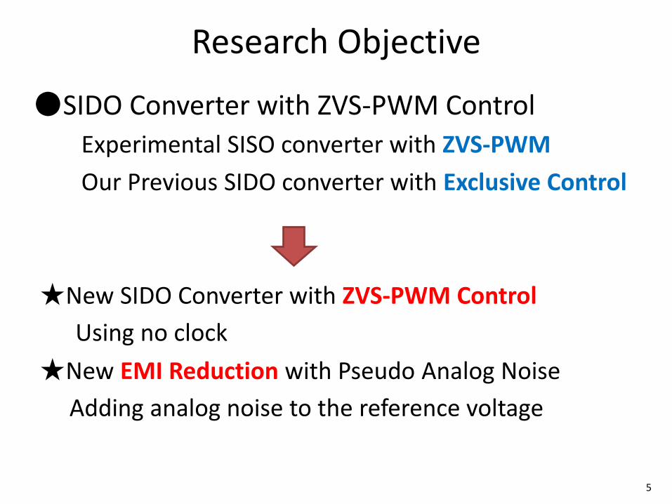
Our Previous SIDO converter with Exclusive Control
★New SIDO Converter with ZVS-PWM Control
Using no clock
★New EMI Reduction with Pseudo Analog Noise
Adding analog noise to the reference voltage
5
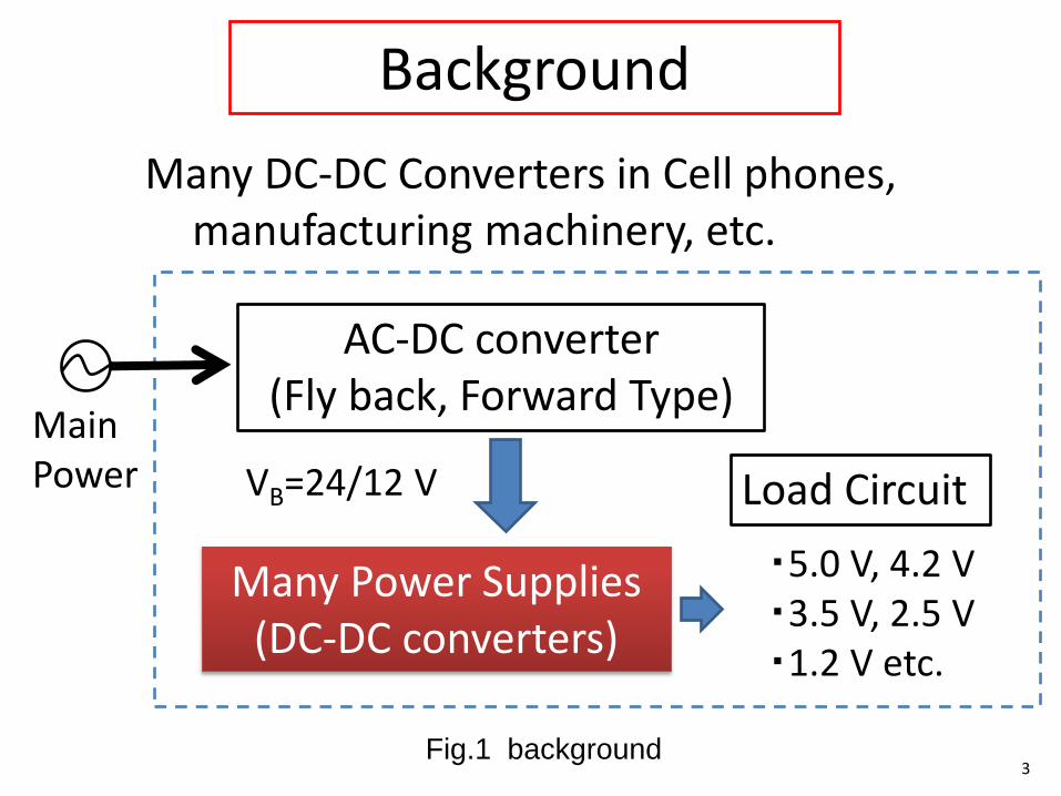
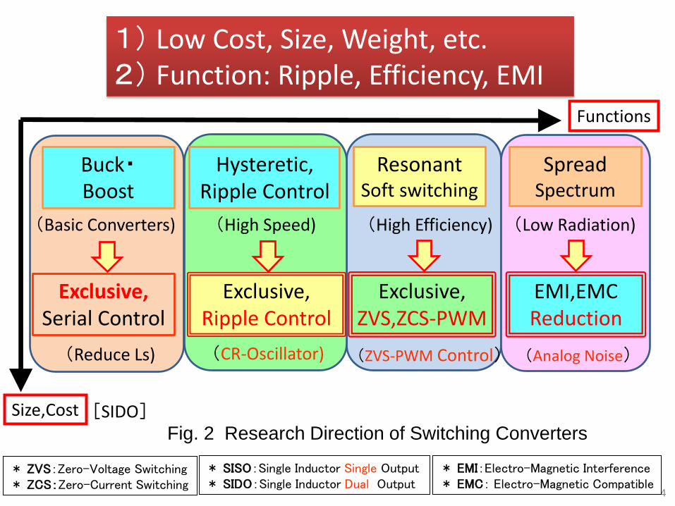
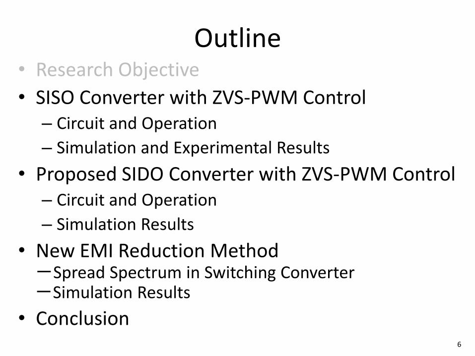
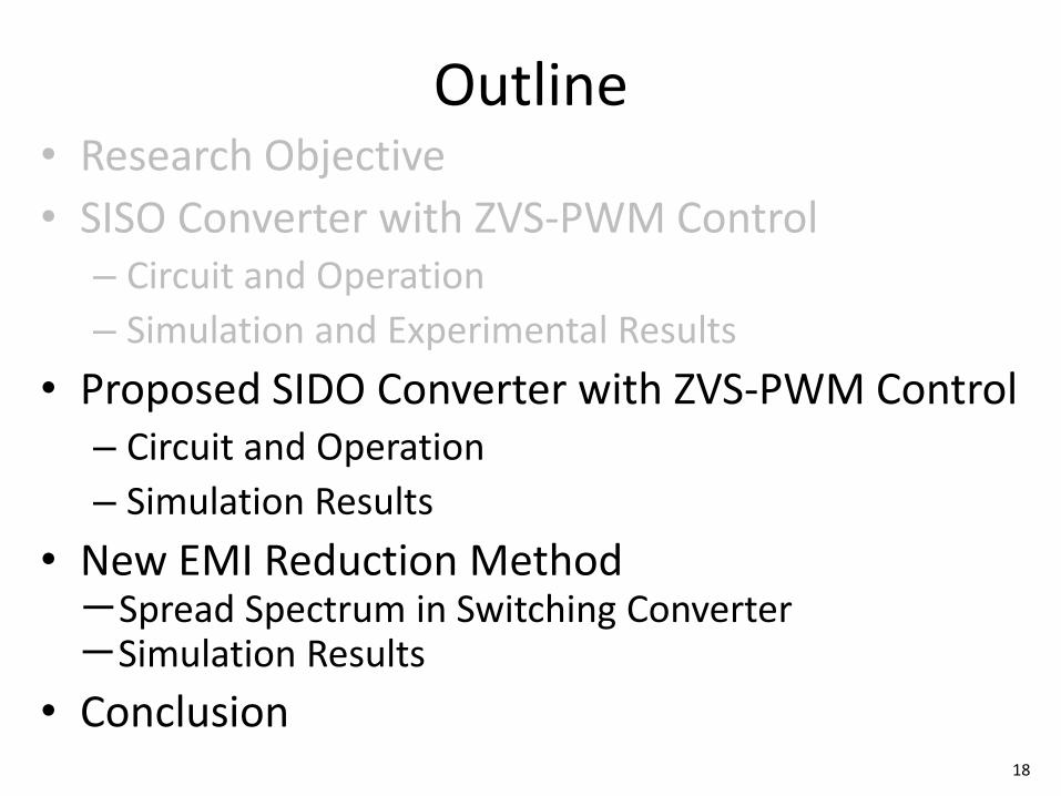
Outline • Research Objective
• SISO Converter with ZVS-PWM Control – Circuit and Operation
– Simulation and Experimental Results
• Proposed SIDO Converter with ZVS-PWM Control – Circuit and Operation
– Simulation Results
• New EMI Reduction Method -Spread Spectrum in Switching Converter -Simulation Results
• Conclusion 6
SISO Buck Converter with ZVS-PWM Control
7
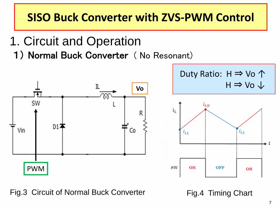
Duty Ratio: H ⇒ Vo ↑ H ⇒ Vo ↓
PWM
Fig.3 Circuit of Normal Buck Converter
1. Circuit and Operation 1) Normal Buck Converter ( No Resonant)
Vo
Fig.4 Timing Chart
SISO Buck Converter with ZVS-PWM Control
8
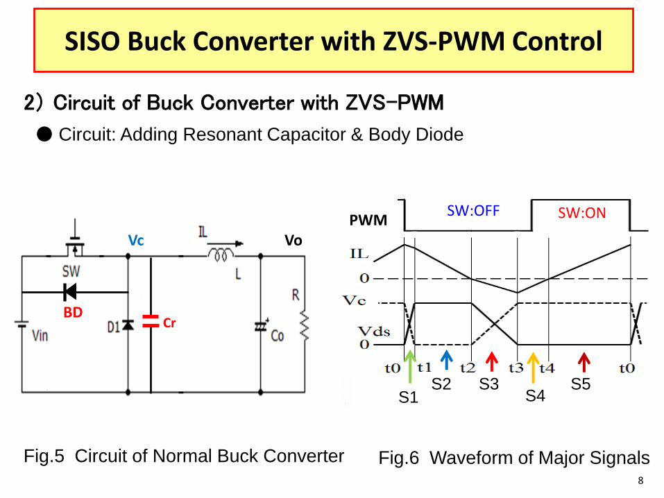
Fig.5 Circuit of Normal Buck Converter
2) Circuit of Buck Converter with ZVS-PWM
Fig.6 Waveform of Major Signals
● Circuit: Adding Resonant Capacitor & Body Diode
Vo
Cr BD
Vc
S1 S2 S3
S4 S5
SW:OFF SW:ON PWM
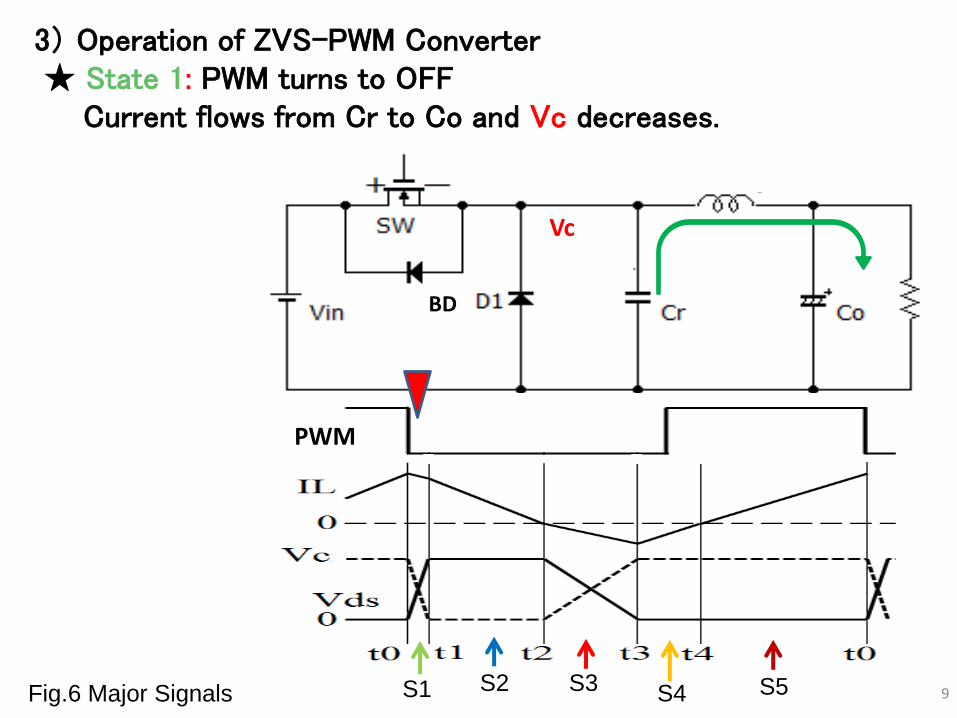
Fig.6 Major Signals S1 S2 S3 S4 S5 9
3) Operation of ZVS-PWM Converter ★ State 1: PWM turns to OFF Current flows from Cr to Co and Vc decreases.
Vc
BD
PWM
Fig.6 Major Signals S1 S2 S3 S4 S5 10
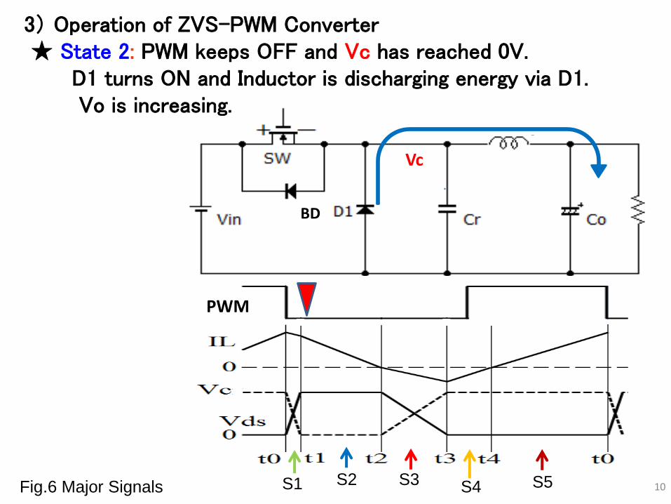
3) Operation of ZVS-PWM Converter ★ State 2: PWM keeps OFF and Vc has reached 0V. D1 turns ON and Inductor is discharging energy via D1. Vo is increasing.
Vc
BD
PWM
Fig.6 Major Signals S1 S2 S3 S4 S5 11
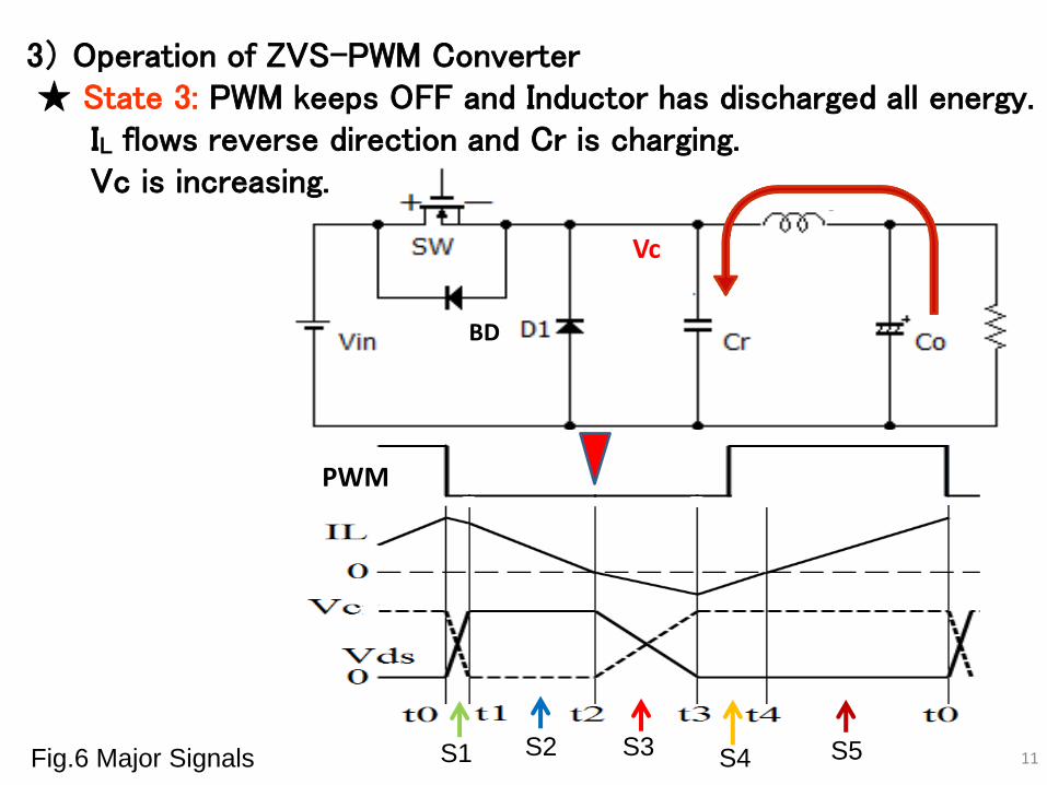
3) Operation of ZVS-PWM Converter ★ State 3: PWM keeps OFF and Inductor has discharged all energy. IL flows reverse direction and Cr is charging. Vc is increasing.
Vc
BD
PWM
Fig.6 Major Signals S1 S2 S3 S4 S5 12
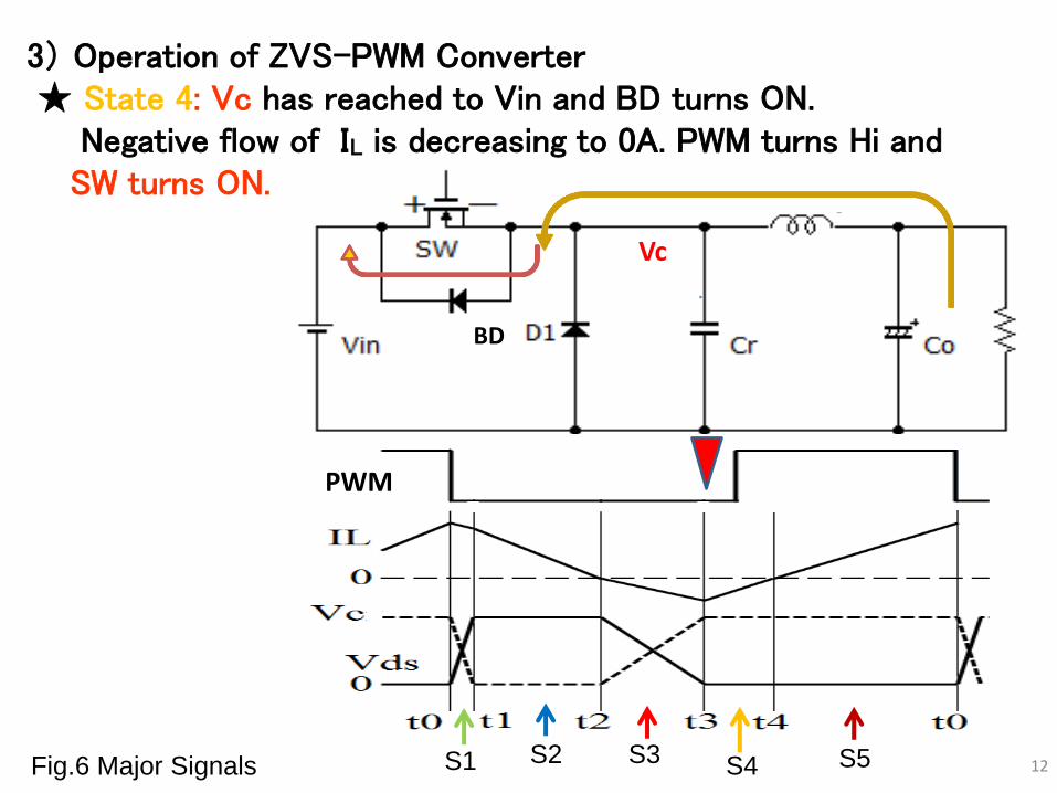
3) Operation of ZVS-PWM Converter ★ State 4: Vc has reached to Vin and BD turns ON. Negative flow of IL is decreasing to 0A. PWM turns Hi and SW turns ON.
Vc
BD
PWM
Fig.6 Major Signals S1 S2 S3 S4 S5 13
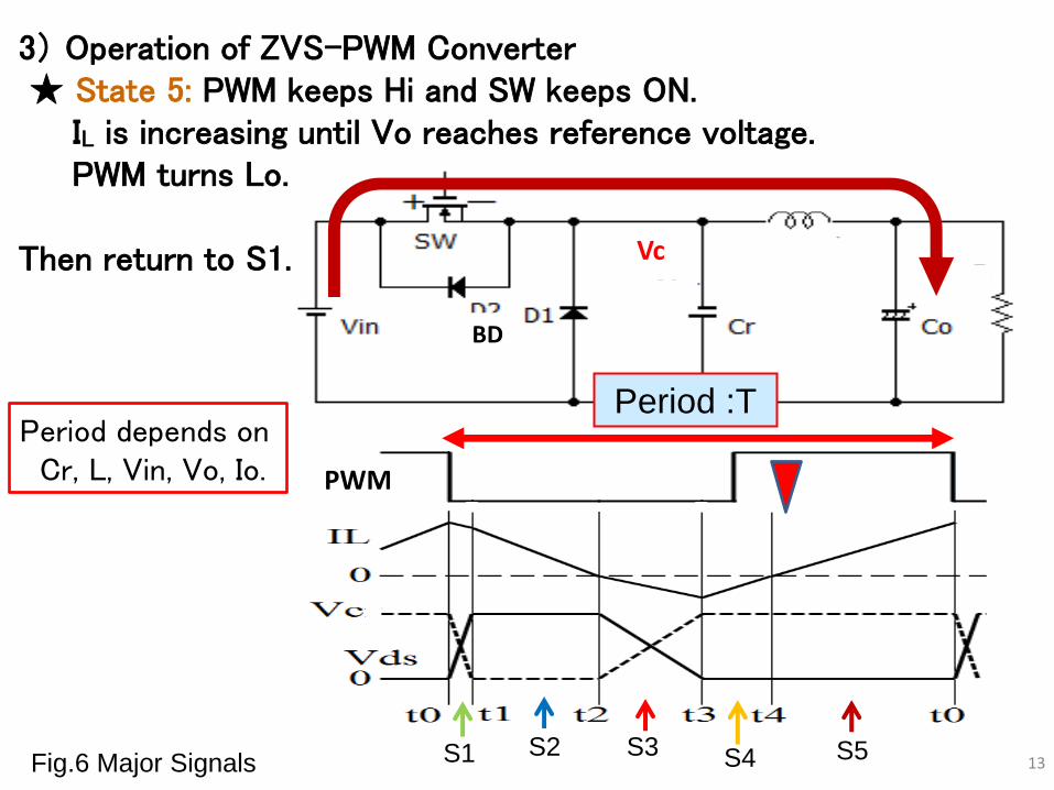
3) Operation of ZVS-PWM Converter ★ State 5: PWM keeps Hi and SW keeps ON. IL is increasing until Vo reaches reference voltage. PWM turns Lo. Then return to S1. Vc
BD
PWM
Period :T Period depends on Cr, L, Vin, Vo, Io.
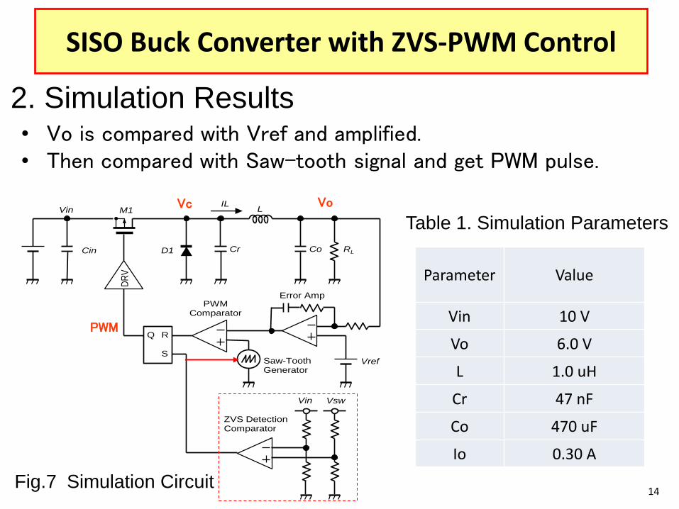
14 Fig.7 Simulation Circuit
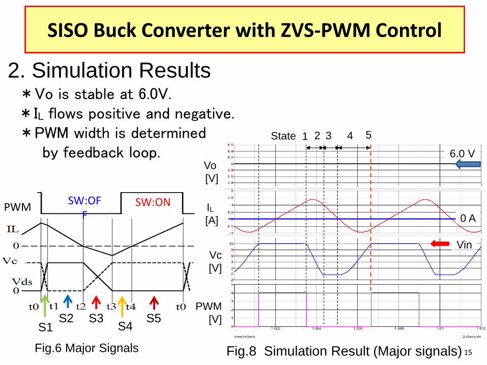
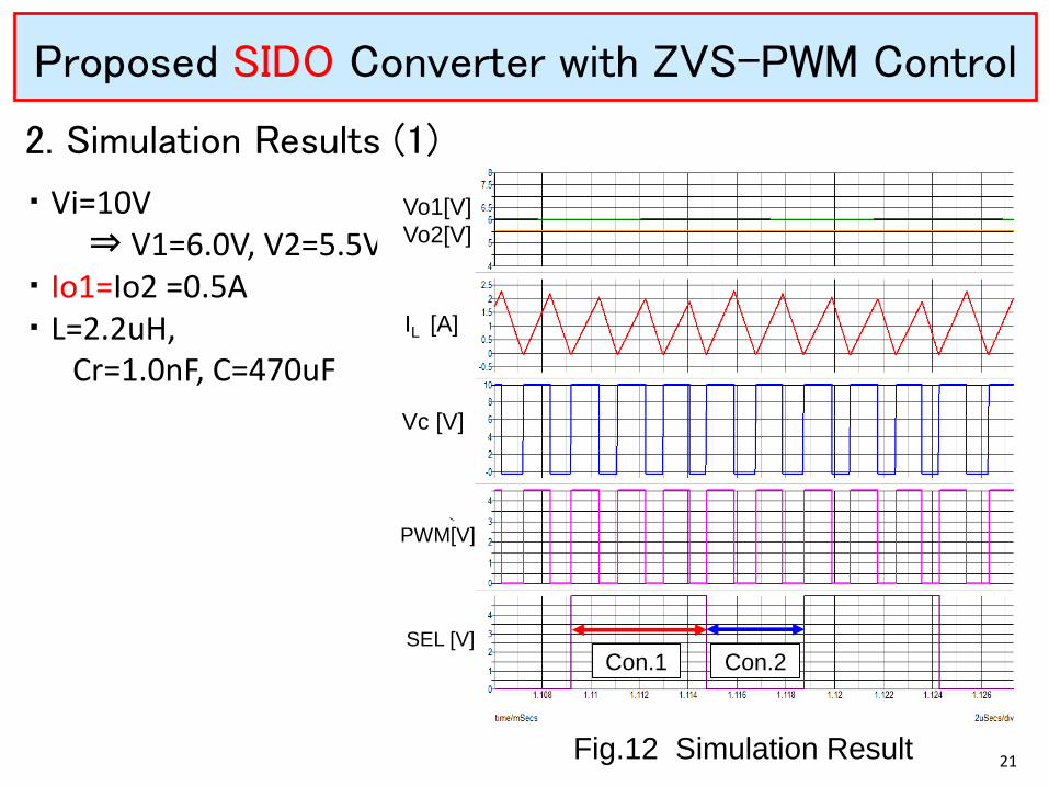
2. Simulation Results
SISO Buck Converter with ZVS-PWM Control
• Vo is compared with Vref and amplified. • Then compared with Saw-tooth signal and get PWM pulse.
DR
V
Vin L
Cr Co RL
Error AmpPWM
Comparator
Saw-ToothGenerator
Vref
Cin
VoVsw
R
S
Q
Vin Vsw
ZVS DetectionComparator
M1
D1
IL
PWM
Vo
Table 1. Simulation Parameters
Parameter Value
Vin 10 V
Vo 6.0 V
L 1.0 uH
Cr 47 nF
Co 470 uF
Io 0.30 A
Vc
S1 S2 S3
S4 S5
SW:OFF
SW:ON PWM
State 2
Vo
[V]
IL
[A]
Vc
[V]
PWM
[V]
3 4 5
15 Fig.8 Simulation Result (Major signals)
2. Simulation Results *Vo is stable at 6.0V. *IL flows positive and negative. *PWM width is determined by feedback loop.
SISO Buck Converter with ZVS-PWM Control
6.0 V
0 A
Vin
Fig.6 Major Signals
1
16
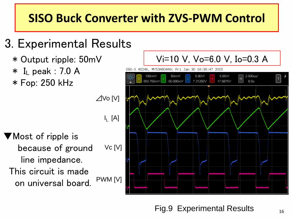
Vi=10 V, Vo=6.0 V, Io=0.3 A * Output ripple: 50mV * IL peak : 7.0 A * Fop: 250 kHz
3. Experimental Results
SISO Buck Converter with ZVS-PWM Control
PWM [V]
⊿Vo [V]
IL [A]
Vc [V]
Fig.9 Experimental Results
▼Most of ripple is because of ground line impedance. This circuit is made on universal board.
17
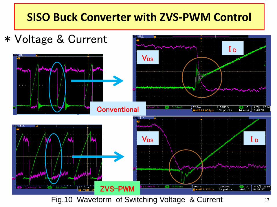
* Voltage & Current
SISO Buck Converter with ZVS-PWM Control
Fig.10 Waveform of Switching Voltage & Current
Conventional
ZVS-PWM
VDS
I D
VDS I D
Outline • Research Objective
• SISO Converter with ZVS-PWM Control – Circuit and Operation
– Simulation and Experimental Results
• Proposed SIDO Converter with ZVS-PWM Control – Circuit and Operation
– Simulation Results
• New EMI Reduction Method -Spread Spectrum in Switching Converter -Simulation Results
• Conclusion 18
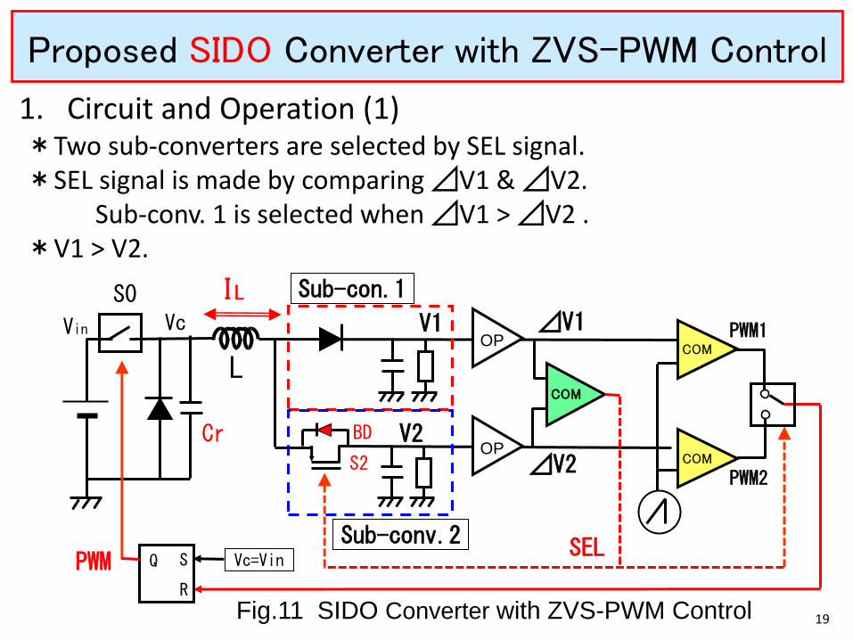
19 Fig.11 SIDO Converter with ZVS-PWM Control
1. Circuit and Operation (1) *Two sub-converters are selected by SEL signal. *SEL signal is made by comparing ⊿V1 & ⊿V2. Sub-conv. 1 is selected when ⊿V1 > ⊿V2 . *V1 > V2.
Proposed SIDO Converter with ZVS-PWM Control
L
S0 ⊿V1
⊿V2
COM PWM1
Sub-con.1
Sub-conv.2
S2
SEL
OP
OP
PWM
COM
PWM2 COM
BD
S
R
Q Vc=Vin
Vc Vin
Cr
IL
V1
V2
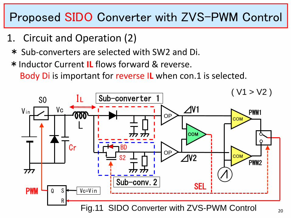
20 Fig.11 SIDO Converter with ZVS-PWM Control
1. Circuit and Operation (2) * Sub-converters are selected with SW2 and Di.
*Inductor Current IL flows forward & reverse. Body Di is important for reverse IL when con.1 is selected.
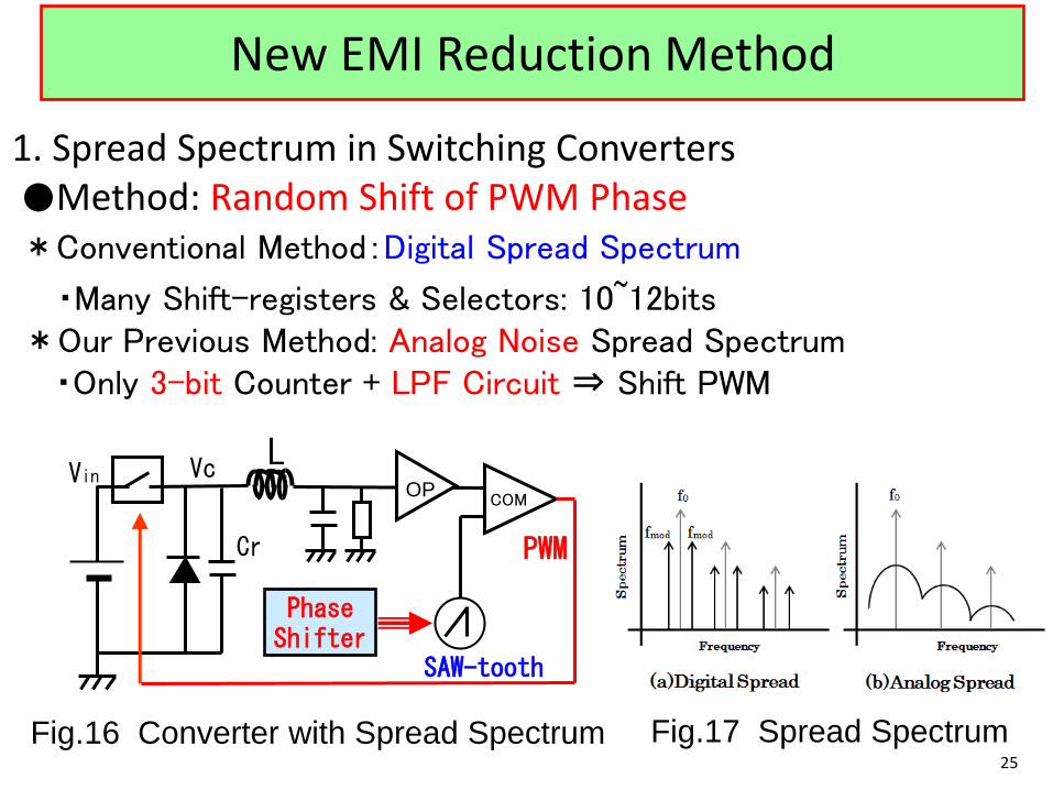
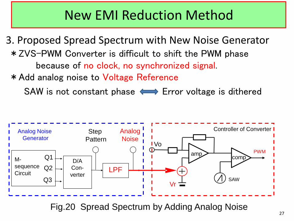
3. Proposed Spread Spectrum with New Noise Generator *ZVS-PWM Converter is difficult to shift the PWM phase because of no clock, no synchronized signal. *Add analog noise to Voltage Reference
SAW is not constant phase Error voltage is dithered
Analog Noise
Generator
Fig.20 Spread Spectrum by Adding Analog Noise
Step Pattern
Analog Noise
D/A Con-
verter LPF
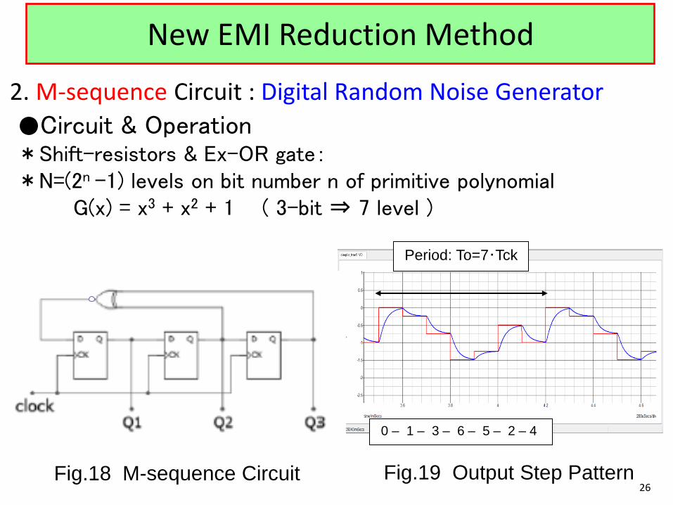
Q1
Q3
Q2
M-
sequence
Circuit
comp amp
Vo
Vr
PWM
SAW
Controller of Converter
New EMI Reduction Method
1.2V 400mV
28
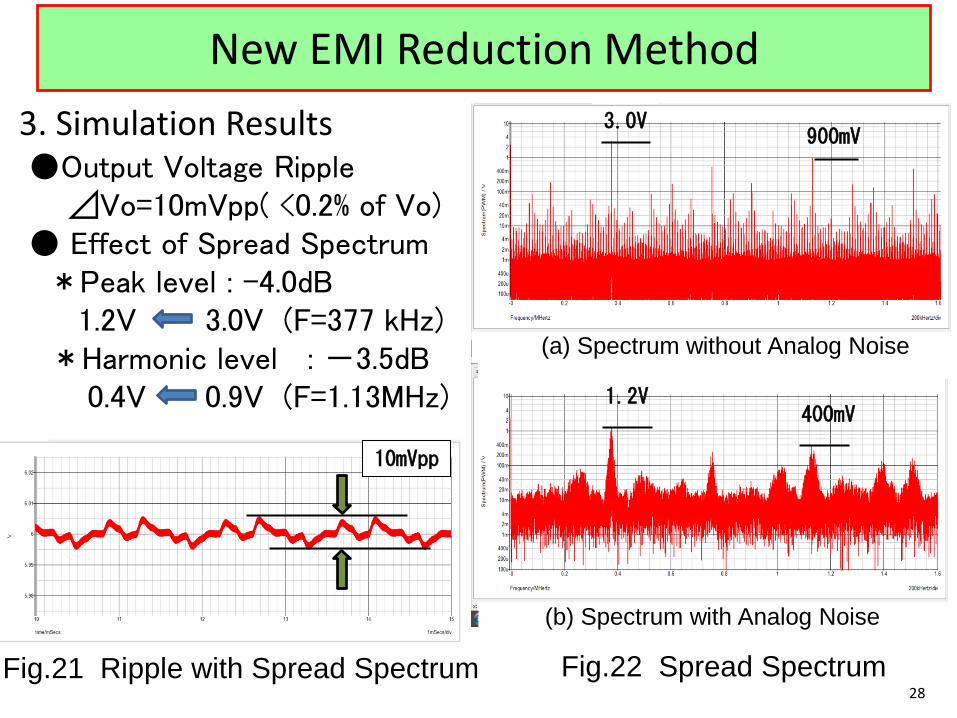
3. Simulation Results ●Output Voltage Ripple ⊿Vo=10mVpp( <0.2% of Vo) ● Effect of Spread Spectrum *Peak level : -4.0dB 1.2V 3.0V (F=377 kHz) *Harmonic level : -3.5dB 0.4V 0.9V (F=1.13MHz)
Fig.22 Spread Spectrum
3.0V 900mV
(a) Spectrum without Analog Noise
(b) Spectrum with Analog Noise
Fig.21 Ripple with Spread Spectrum
10mVpp
New EMI Reduction Method
Conclusion
29
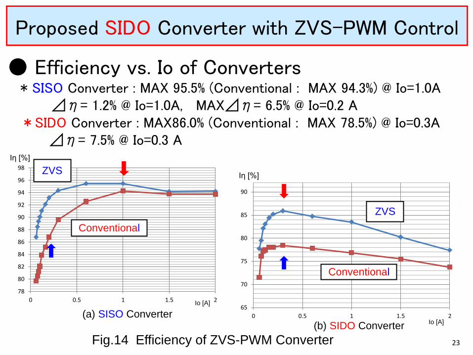
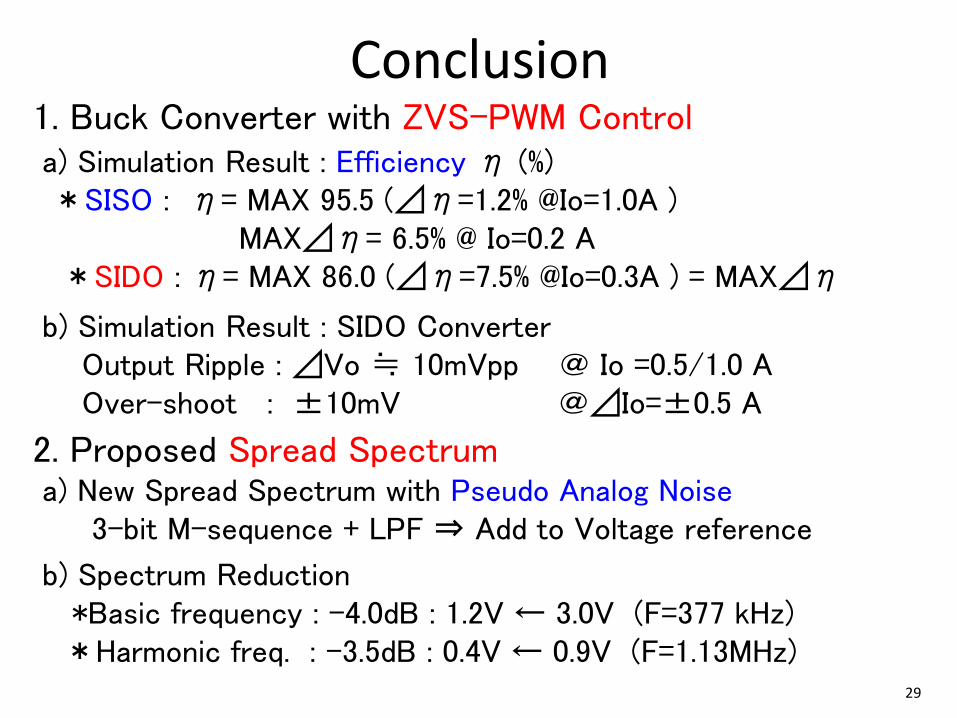
1. Buck Converter with ZVS-PWM Control a) Simulation Result : Efficiency η (%) *SISO : η= MAX 95.5 (⊿η=1.2% @Io=1.0A ) MAX⊿η= 6.5% @ Io=0.2 A *SIDO : η= MAX 86.0 (⊿η=7.5% @Io=0.3A ) = MAX⊿η
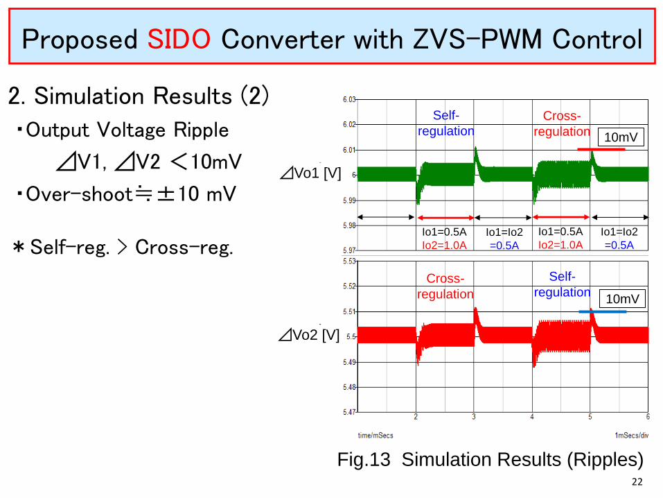
b) Simulation Result : SIDO Converter Output Ripple : ⊿Vo ≒ 10mVpp @ Io =0.5/1.0 A Over-shoot : ±10mV @⊿Io=±0.5 A
2. Proposed Spread Spectrum a) New Spread Spectrum with Pseudo Analog Noise 3-bit M-sequence + LPF ⇒ Add to Voltage reference


![Fuzzy Controlled ZVS Asymmetrical PWM Full-bridge DC-DC ... · robust fuzzy logic controller and fuzzy load conductance observer for DC-DC boost converter is designed [16]. State](https://static.documents.pub/doc/80x56/5f4a3cdbda168c151e4e1cc6/fuzzy-controlled-zvs-asymmetrical-pwm-full-bridge-dc-dc-robust-fuzzy-logic-controller.jpg)


![Survey stability of the ZVS phase-shifted full-bridge DC ...journal.it.cas.cz/62(2017)-KHO/Paper Sharif260.pdf · ZVS PWM in [4] is formed by a diode, a resonant capacitor and a resistor.](https://static.documents.pub/doc/80x56/5e3125c4d23e5149907b5255/survey-stability-of-the-zvs-phase-shifted-full-bridge-dc-2017-khopaper-sharif260pdf.jpg)