TM Low-cost Sensor Signal Conditioner Datasheet PRELIMINARY
Features • Digital compensation of sensor offset, sensitivity,
temperature drift and non-linearity • Accommodates differential sensor signal spans
from 1.2mV/V to 36mV/V • Digital one-shot calibration via one-wire interface:
quick and precise • Internal temperature compensation reference • Output options: ratiometric analog voltage,
absolute analog voltage, digital one-wire-interface • Supply voltage 2.7 to 5.5V, with external JFET 5.5
to 30V • Current consumption depends on programmed
sample rate. 1mA maximum down to 250µA • Operation temperature –50 to +150°C • Fast response time: 1ms • High voltage protection up to 30V with external
JFET • No external trimming components required • PC-controlled configuration and calibration via
one-wire interface - simple, low cost • High accuracy (±0.1% FSO @ -25 to 85°C;
±0.25% FSO @ -40 to 125°C)
Application Circuit
Typical RBic LiteTM Application Circuit
Brief Description The RBicLite
TM is a CMOS integrated circuit for highly-accurate amplification and sensor-specific correction of bridge sensor signals. Digital compensation of sensor offset, sensitivity, temperature drift and non-linearity is accomplished via an internal digital signal processor running a correction algorithm with calibration coefficients stored in a non-volatile EEPROM. The RBicLite
TM is adjustable to nearly all piezo-resistive bridge sensors. Measured and corrected bridge values are provided at SIGTM pin, which can be configured as an analog voltage output or as one-wire serial digital output. The digital one-wire-interface can be used for a simple PC-controlled calibration procedure, in order to program a set of calibration coefficients into an on-chip EEPROM. Thus a specific sensor and a RBicLite
TM are mated digitally: fast, precise and without the cost overhead associated with trimming by external devices or laser. • Development kit available, containing PCB,
SOP8 samples, software, documentation • Support for industrial mass calibration
available • Quick circuit customization possible for large
TM Low-cost Sensor Signal Conditioner Datasheet PRELIMINARY
1 CIRCUIT DESCRIPTION ........................................................................................................................................4 1.1 SIGNAL FLOW AND BLOCK DIAGRAM ...................................................................................................................4 1.2 ANALOG FRONT END.............................................................................................................................................5
1.2.1 Bandgap/PTAT and PTAT Amplifier ............................................................................................................5 1.2.2 Bridge Supply................................................................................................................................................5 1.2.3 Pre-Amp Block..............................................................................................................................................5 1.2.4 Analog to Digital Converter (ADC)..............................................................................................................5
1.3 DIGITAL SIGNAL PROCESSOR ................................................................................................................................6 1.3.1 Coefficient Memory (EEPROM) ...................................................................................................................7 1.3.2 One-Wire Interface - ZACwireTM..................................................................................................................7
1.4 OUTPUT STAGE......................................................................................................................................................8 1.4.1 Digital to Analog Converter (Output DAC)..................................................................................................8 1.4.2 Output Buffer ................................................................................................................................................8 1.4.3 Voltage Reference Block ...............................................................................................................................8
1.5 CLOCK GENERATOR / POWER ON CLEAR (CLKPOC) ...........................................................................................8 1.5.1 Trimming the Oscillator................................................................................................................................8
2 FUNCTIONAL DESCRIPTION...............................................................................................................................9 2.1 GENERAL WORKING MODE...................................................................................................................................9 2.2 ZAC WIRETM COMMUNICATION PROTOCOL .......................................................................................................10
2.2.1 Bit Encoding ...............................................................................................................................................10 2.2.2 Packet Frame from Calibration Master to IC ............................................................................................10 2.2.3 High Level Protocol....................................................................................................................................11
2.6.1 Correction Coefficients...............................................................................................................................20 2.6.2 Interpretation of Binary Numbers for Correction Coefficients: .................................................................20
2.7 READ OF EEPROM CONTENTS ...........................................................................................................................23 3 APPLICATION CIRCUIT EXAMPLES...............................................................................................................25
3.1 THREE-WIRE RATIOMETRIC OUTPUT ..................................................................................................................25 3.2 ANALOG VOLTAGE OUTPUT................................................................................................................................26 3.3 THREE-WIRE RATIOMETRIC OUTPUT WITH OVER-VOLTAGE PROTECTION .........................................................26 3.4 DIGITAL OUTPUT.................................................................................................................................................27
4 ESD/LATCH-UP-PROTECTION ..........................................................................................................................27 5 PIN CONFIGURATION AND PACKAGE ...........................................................................................................28
TM Low-cost Sensor Signal Conditioner Datasheet PRELIMINARY
6 IC CHARACTERISTICS ........................................................................................................................................29 6.1 ABSOLUTE MAXIMUM RATINGS..........................................................................................................................29 6.2 RECOMMENDED OPERATING CONDITIONS...........................................................................................................29 6.3 ELECTRICAL PARAMETERS ..................................................................................................................................30 6.4 ANALOG INPUTS..................................................................................................................................................31 6.5 TEMPERATURE COMPENSATION AND TEMPERATURE OUTPUT ............................................................................31 6.6 HIGH VOLTAGE OPERATION................................................................................................................................32
TM Low-cost Sensor Signal Conditioner Datasheet PRELIMINARY
1 Circuit Description
1.1 Signal Flow and Block Diagram The RBicLite
TM series of resistive bridge sensor interface ICs were specifically designed as a cost-effective solution for sensing in building automation, industrial, office automation and white goods applications. The RBicLite
TM employs ZMD’s high precision bandgap with proportional-to-absolute-temperature (PTAT) output; low-power 14-bit ADC; and on-chip DSP core with EEPROM to precisely calibrate the bridge output signal. Three selectable outputs, two analog and one digital, offer the ultimate in versatility across many applications. The RBicLite’s ratiometric 5~95% Vout signal (0.25~4.75 Vout @ VDD=5V) suits most building automation and automotive requirements. Typical office automation and white goods applications require the 0~1Vout signal, which in the RBic LiteTM is referenced to the internal bandgap. Direct interfacing to µP controllers is facilitated via ZMD’s single-wire serial ZACwireTM digital interface. RBicLite
TM is capable of running in high-voltage (5.5-30V) systems when combined with an external JFET.
TM Low-cost Sensor Signal Conditioner Datasheet PRELIMINARY
1.2 Analog Front End
1.2.1 Bandgap/PTAT and PTAT Amplifier The Bandgap/PTAT provides the PTAT signal to the ADC, which allows accurate temperature conversion. In addition, the ultra-low ppm Bandgap provides a stable voltage reference over temperature for the operation of the rest of the IC. The PTAT signal is amplified through a path in the pre-amp and fed to the ADC for conversion. The most significant 12-bits of this converted result are used for temperature measurement and temperature correction of bridge readings. When temperature is output in digital mode only the most significant 8-bits are given.
1.2.2 Bridge Supply The voltage driven bridge is usually connected to VDD and ground. As a power savings feature, the RBIClite also includes a switched transistor to interrupt the bridge current via pin 1 (Bsink). The transistor switching is synchronized to the A-to-D conversion and released after finishing the conversion. To utilize this feature, the low supply of the bridge should be connected to Bsink instead of ground. Depending on the programmable update rate, the average current consumption (including bridge current) can be reduced to approximately 20%, 5% or 1%.
1.2.3 Pre-Amp Block The differential signal from the bridge is amplified through a chopper-stabilized instrumentation amplifier with very high input impedance designed for low noise and low drift. This pre-amp will gain the differential signal and re-center its DC to VDD/2. The output of the Pre-Amp Block is fed into the A-to-D converter. The calibration sequence performed by the digital core includes an auto zero sequence to null any drift in the Pre-Amp state over temperature. The PreAmp is nominally set to a gain of 24. The inputs to the PreAmp from (VBN/VBP pins) can be reversed via an EEPROM config bit.
1.2.4 Analog to Digital Converter (ADC) A 14-bit/1ms 2nd order charge-balancing analog-to-digital converter is used to convert signals coming from the pre-amplifier. The converter, designed in full differential switched capacitor technique, is used for converting the various signals in the digital domain. This principle offers the following advantages:
• High noise immunity because of the differential signal path and integrating behavior • Independent from clock frequency drift and clock jitter • Fast conversion time owing to second order mode
Four selectable values for the zero point of the input voltage allow conversion to adapt to the sensor’s offset parameter. Together with the reverse input polarity mode, this results in four possible zero point adjustments. The conversion rate varies with the programmed update rate. The fastest conversation rate is 1k samples/s and the response time is then 1ms. Based on a best fit, the Integral Nonlinearity (INL) is less then 4 LSB14Bit.
TM Low-cost Sensor Signal Conditioner Datasheet PRELIMINARY
1.3 Digital Signal Processor A digital signal processor (DSP) is used for processing the converted bridge data as well as performing temperature correction, and computing temperature value for output on the digital channel. The digital core reads correction coefficients from EEPROM, and can correct for:
1. Bridge Offset 2. Bridge Gain 3. Variation of Bridge offset over Temperature (Tco) 4. Variation of Bridge gain over Temperature (Tcg) 5. A single second order effect (SOT) (Second Order Term)
The EEPROM contains a single SOT that can be applied to correct one and only one of the following
• 2nd Order behavior of bridge measurement • 2nd Order behavior of Tco • 2nd Order behavior of Tcg
If the SOT applies to correcting the bridge reading then the correction formula for the bridge reading is represented as a two step process as follows: ZB = GainB[1 + ∆T*Tcg]*[BR_Raw + OffsetB + ∆T*Tco] BR = ZB*(1.25+SOT*ZB) Where: BR = Corrected Bridge reading that is output as digital or analog on SIGTM pin. ZB = Intermediate result in the calculations. BR_Raw = Raw Bridge reading from A2D. T_Raw = Raw Temp reading converted from PTAT signal GainB = Bridge gain term OffsetB = Bridge offset term Tcg = Temperature coefficient gain Tco = Temperature coefficient offset ∆T = (T_Raw - TSETL) T_Raw = Raw Temp reading converted from PTAT signal TSETL = T_Raw reading at which low calibration was performed (typically 25C) SOT = Second Order Term If the SOT applies to correcting 2nd Order behavior of Tco then the formula for bridge correction is as follows: BR = GainB[1 + ∆T*Tcg]*[BR_Raw + OffsetB + ∆T(SOT*∆T + Tco)]
TM Low-cost Sensor Signal Conditioner Datasheet PRELIMINARY
If the SOT applies to correcting 2nd Order behavior of Tcg then the formula for bridge correction is as follows: BR = GainB[1 + ∆T(SOT*∆T + Tcg)]*[BR_Raw + OffsetB + ∆T*Tco)] The bandgap reference gives a very linear PTAT signal, so temperature correction can always simply be accomplished with a linear gain and offset term. Corrected Temp Reading: T = GainT*[T_Raw + OffsetT] Where: T_Raw = Raw Temp reading converted from PTAT signal OffsetT = TempSensor offset coefficient GainT = TempSensor gain coefficient
1.3.1 Coefficient Memory (EEPROM) The EEPROM contains the calibration coefficients for gain and offset, etc., and the configuration bits, such as output mode, update rate, etc. When programming the EEPROM, an internal charge pump voltage is used thus a high voltage supply is not needed.
The charge pump is internally regulated to 12.5 V voltage and the programming time amounts to 6ms.
1.3.2 One-Wire Interface - ZACwireTM The IC communicates via a one-wire serial interface. There are different commands available for:
• Reading the conversion result of the ADC (Get BR_Raw, Get T_Raw) • Calibration Commands • Entering various test modes
o DAC test modes o Oscillator, 1V, and Pre-Amp o EEPROM test modes o Oscillator override & Scan test modes
• Reading from the EEPROM (dump of entire contents) • Writing to the EEPROM (trim setting, configuration, and coefficients)
TM Low-cost Sensor Signal Conditioner Datasheet PRELIMINARY
1.4 Output Stage 1.4.1 Digital to Analog Converter (Output DAC) An 11-bit DAC based on sub-ranging resistor strings is used for the digital-to-analog output conversion in the analog ratiometric and absolute modes. Selection during calibration configures the system to operate in either of these modes. The design allows for excellent testability as well as low power consumption.
1.4.2 Output Buffer A rail-to-rail op amp configured as a unity gain buffer can drive resistive loads (whether pull-up or pull-down) as low as 2.5kΩ and capacitances up to 15nF. In addition, to limit the error due to amplifier offset voltage, an error compensation circuit is included which tracks and reduces offset voltage to < 1mV.
1.4.3 Voltage Reference Block This block uses the absolute reference voltage provided by the bandgap to produce two regulated on-chip voltage references. A 1V reference is used for the output DAC high reference when the part is configured in 0-1V analog output mode. For this reason, the 1V reference must be very accurate and includes trim so that its value can be trimmed within +/- 2mV of 1.00V. The 1V reference is also used as the on-chip reference for the JFET regulator block. Thus the regulation set point of the JFET regulator can be fine tuned using the 1V trim.
1.5 Clock Generator / Power On Clear (CLKPOC) If the power supply exceeds 2.5V (maximum), the reset signal de-asserts and the clock generator starts working at a frequency of approximately 512kHz (±20%). The exact value only influences the conversion cycle time and communication to the outside world but not the accuracy of signal processing. In addition, to minimize the oscillator error as the VDD voltage changes, an on-chip regulator is used to supply the oscillator block.
1.5.1 Trimming the Oscillator Trimming is performed at wafer level, and it is strongly recommended that this not be changed during calibration, as ZAC wireTM communication is no longer guaranteed at different oscillator frequencies.
Trimming Bits Delta Frequency (KHz)
100 +385
101 +235
110 +140
111 +65
000 Nominal 001 -40 010 -76 011 -110
Sample: Programming ”011” → the trimmed frequency = nominal value – 110KHz
TM Low-cost Sensor Signal Conditioner Datasheet PRELIMINARY
2 Functional Description
2.1 General Working Mode The command/data transfer takes place via the one-wire SigTM pin using the ZAC WireTM serial communication protocol. After Power ON the IC is waiting for 6ms(=Command window) for the Start_CM command. Without this command the NOM(Normal Operation Mode) starts and dependent from the EEPROM contents the bridge raw values will be corrected and the calculated values will appear at the output (analog or digital). Any of the modes can only be entered by a new power ON. If the IC receives the Start_CM command during the command window it remains in the command mode. The CM allows changing in one of the other modes by command. After command Start_RW the IC is in the Raw mode. Without calculation the raw values are transmitted to the digital output in a predefined order. The RM can only be stopped by Power Off.
TM Low-cost Sensor Signal Conditioner Datasheet PRELIMINARY
2.2 ZAC WireTM Communication Protocol
2.2.1 Bit Encoding Duty cycle encoded Manchester: Start bit => 50% duty cycle used to set up strobe time Logic 1 => 75% duty cycle Logic 0 => 25% duty cycle
2.2.2 Packet Frame from Calibration Master to IC RBicLite
TM IC will receive a 19-bit frame: The incoming serial signal will be-sampled at a 512kHz clock rate. This protocol is very tolerant to clock skew and can easily tolerate baud rates in the (6kHz 48kHz) range. The incoming frame will be checked for proper parity on both command and data bytes, as well as for any edge timeouts prior to a full frame being received. Once a command data pair is received, the RBicLite
TM will perform that command. Once the command has been successfully executed by the IC, it will acknowledge success by a transmission of an A5H byte back to the master. If the master does not receive an A5H transmission within 130msec of issuing the command, it must assume the command was either improperly received or could not be executed. The RBicLite
TM will transmit 9-bit bytes (8-data, 1-parity). During calibration and configuration, transmissions will normally be either A5H, or data. A5H indicates successful completion of command. During Normal Operation Mode (NOP), if the part is configured for digital output, the bridge reading will be transmitted first, optionally followed by the temperature byte. The high byte of bridge will be sent first, followed by the low byte.
Bit window
Start Bit Cmd Bit (7) Cmd Bit (0) Parity_cmd Data Bit (7) Data Bit (0) Parity_data
TM Low-cost Sensor Signal Conditioner Datasheet PRELIMINARY
Transmissions from the IC will occur at one of two speeds depending on the update rate programmed in EEPROM. If the user chooses one of the two fastest update rates (1ms or 5ms) then the baud rate of digital transmission will be 32kHz. If however, the user chooses one of the two slower update rates (25ms or 125ms) then the baud rate of digital transmission will be 8kHz. One can easily program any standard µController to communicate with the RbicLite
TM. ZMDA can provide sample code for a MicroChip PIC µController.
2.2.3 High Level Protocol The RBicLite
TM will listen for a command/data pair to be transmitted for the 6ms after the de-assert of its internal Power On Reset (POR). If a transmission is not received within this time frame, then it will transition to Normal Operation Mode (NOP). In the NOP, it will output bridge data in either 0-1V analog, 5%-95% ratiometric analog, or digital depending on how the part is currently configured. If the RBicLite
TM receives a Start CM command within the first 6ms after the de-assert of POR, then it will go into Command Mode(CM). In this mode, calibration/configuration commands will be executed. The RBicLite
TM will acknowledge successful execution of commands by transmission of A5H. The calibrating/configuring master will know a command was not successfully executed if no response is received after 130ms of issuing the command. Once in command interpreting/executing mode, the RBicLite
TM will stay in this mode until power is removed, or a Start NOM (Start Normal Operation Mode) command is received. The START CM command is used as an interlock mechanism to prevent a spurious entry into command mode on power up. The first command received within the 6ms window of POR must be a START CM command to enter into command interpreting mode. Any other commands will be ignored.
2.3 Command/Data Pair Encoding The 16-bit command/data stream sent to the RBicLite
TM can be broken into four 4-bit nibbles. The most significant nibble encodes the command. The 2nd nibble is reserved for possible future expansion, and should be sent as “0x0”. The last two nibbles encode the data byte.
TM Low-cost Sensor Signal Conditioner Datasheet PRELIMINARY
Command nibble: Data: Description: 0H 0XXH Read EEPROM Command via SIGTM pin. 2H 0YXH Enter Test Mode (Subset of command mode for testing
purpose only): SIGTM pin will assume the value of different internal test points, depending on most significant nibble of data sent. Y = 0H => Internal oscillator Y = 1H => 2.5V reference Y = 2H => PTAT Y = 3H => Pre-Amp Output+ Y = 4H => Scan Mode (SDO routed to SIG TM pin, part goes into Clock Override Mode and Scan Mode) Y = 5H => DAC Ramp testmode. Gain_b[13:3] contains the starting point, and the increment is (offset_b/8). The increment will be added every 125usec. Y = 6-7H => Part goes into Clock Override Mode. Y = 8-FH => Undefined.
TM Low-cost Sensor Signal Conditioner Datasheet PRELIMINARY
Command nibble: Data: Description: 4H 000H Start NOM => Ends Command Mode, transition to Normal
Operation Mode Mode.
4H 010H Start Raw Mode (RM) In this mode if Gain_B = 800H, and Gain_T = 80H then the digital output will simply be the raw values of the A2D for the Bridge reading, and the PTAT conversion.
5H 000H START CM => Start the Command Mode, used to enter command interpret mode. If data is sent with this command then that data sets up the start data for the DAC Test Mode.
6H 0YYH Program SOT (2nd Order Term). 7H 0YYH Program TSETL 8H 0YYH Program GainB upper 7-bits 9H 0YYH Program GainB lower 8-bits AH 0YYH Program OffsetB upper 6-bits BH 0YYH Program OffsetB lower 8-bits CH 0YYH Program GainT DH 0YYH Program OffsetT EH 0YYH Program Tco FH 0YYH Program Tcg
TM Low-cost Sensor Signal Conditioner Datasheet PRELIMINARY
2.4 Calibration Sequence Although the RBicLite
TM IC can work with many different types of resistive bridges, lets assume a pressure bridge for the following discussion on calibration. Calibration essentially involves collecting raw bridge and temperature data from the IC for different known pressures and temperatures. This raw data can then be “crunched” by the calibration master (lets assume a PC), and the calculated coefficients can then be written to the IC. ZMDA can provide software and hardware with samples to perform the calibration. There are three main steps to calibration:
1. Assigning a unique identification to the IC. This identification is programmed in EEPROM and can be used as an index into the database stored on the calibration PC. This database will contain all the raw values of bridge readings and temp reading for that part, as well as the known pressure and temperature the bridge was exposed to. This unique identification can be stored in a combination of the following EEPROM registers TSETL, Tcg,Tco. These registers will be overwritten at the end of the calibration process, so this unique identification is not a permanent serial number.
2. Data collection. Data collection involves getting raw data from the bridge at different known pressures and temperatures. This data is then stored on the calibration PC using the unique identification of the IC as the index to the database.
3. Coefficient calculation and write. Once enough data points have been collected to calculate all the desired coefficients then the coefficients can be calculated by the calibrating PC and written to the IC.
Step 1 Assigning Unique Identification Assigning a unique identification number is as simple as using the commands Program TSETL, Program Tcg, and Program Tco. These 3 8-bit registers will allow for 16Meg unique devices. In addition Gain_B needs to be programmed to 800H (unity) and Gain_T needs to be programmed to 80H (unity). Step 2 Data Collection The number of different unique (pressure, temperature) points that calibration needs to be performed at depends on the customer’s needs. The minimum is a 2-point calibration, and the maximum is a 5-point calibration. To acquire raw data from the part one has to get RBicLite
TM to enter Raw Mode. This is done by issuing a Start CM (Start Command Mode 5000H) command to the IC followed by a Start RM (Start Raw Mode 4010H) command with the LSB of the upper data nibble set. Now if the Gain_B term was set to unity (800H) and the Gain_T term was also set to unity (80H) then the part will be in the Raw Mode and will be outputting raw data on its SIGTM pin instead of corrected bridge and temperature. The calibration system should now grab several of these data points (16 each of bridge and temperature is recommended) and average them. These raw bridge and temperature setting should be stored in the database along with the known pressure and temperature. The ouput format during Raw Mode is Bridge_High, Bridge_Low, Temp. Each of these being 8-bit quantities. The upper 2-bits of Bridge_High are zero filled. The Temp data (8-bits only) would not really be enough info for accurate temperature calibration. Therefore the upper three bits of temp information are not given, but rather assumed known. Therefore effectively 11-bits of temperature information is provided in this mode.
TM Low-cost Sensor Signal Conditioner Datasheet PRELIMINARY
Step 3 Coefficient Calculations The math to perform the coefficient calculation is very complicated and will not be discussed in detail. There is a rough overview in the “Calibration Math” section. Rather ZMDA will provide software to perform the coefficient calculation. ZMDA can also provide source code of the algorithms in a C code format. Once the coefficients are calculated the final step is to write them to the EEPROM of the RBicLite
TM. The number of calibration points required can be as few as two or as many as five. This depends on the precision desired, and the behavior of the resistive bridge in use.
1. 2-point calibration would be used if one simply wanted a gain and offset term for a bridge with no temperature compensation for either term.
2. 3-point calibration would be used if one wanted to have 1st order compensation for either a Tco or Tcg term but not both.
3. 3-point calibration could also be used if one wanted 2nd order correction for the bridge, but no temperature compensation of the bridge output.
4. 4-point calibration would be used if one wanted 1st order compensation for both Tco and Tcg 5. 4-point calibration could also be used if one wanted 1st order compensation for either Tco or Tcg but
not both, and wanted 2nd order correction for the bridge measurement. 6. 5-point calibration would be used if one wanted both 1st order Tco correction and 1st order Tcg
correction, plus a 2nd order correction that could be applied to one and only one of the following: 2nd order Tco, 2nd order Tcg, or 2nd order bridge.
TM Low-cost Sensor Signal Conditioner Datasheet PRELIMINARY
EEPROM Range
Description Note
14:13 Config Jfet Regulation
00 => No JFET regulation (lower power) 01 => No JFET regulation (lower power) 10 => JFET regulation centered around 5.0V 11 => JFET regulation centered around 5.5V (i.e. overvoltage protection).
29:15 Gain_B Bridge Gain: Gain_B[14] => mult x 8 Gain_B[13:0] => 14-bit unsigned number representing a number in the range [0,8).
43:30 Offset_B Signed 14-bit offset for bridge correction 51:44 Gain_T Temperature gain coefficient used to correct
PTAT reading. 59:52 Offset_T Temperature offset coefficient used to correct
PTAT reading. 67:60 TSETL Stores Raw PTAT reading at temperature in
which low calibration points were taken 75:68 Tcg Coefficient for temperature correction of bridge
gain term. Tcg = 8-bit magnitude of Tcg term. Sign is determined by tc_cfg (bits 87:84)
83:76 Tco Coefficient for temperature correction of bridge offset term. Tco = 8-bit magnitude of Tco term. Sign and scaling are determined by tc_cfg (bits 87:84)
87:84 Tc_cfg This 4-bit term determines options for Temperature compensation of the bridge. Tc_cfg[3] => If set, Bridge Signal Polarity flips Tc_cfg[2] => If set Tcg is negative Tc_cfg[1] => Scale magnitude of Tco term by 8 Tc_cfg[0] => If set Tco is negative
TM Low-cost Sensor Signal Conditioner Datasheet PRELIMINARY
EEPROM Range
Description Note
95:88 SOT 2nd Order Term. This term is a 7-bit magnitude with sign. SOT[7] = 1 negative SOT[7] = 0 positive SOT[6:0] = magnitude [0-127] This term can apply to a 2nd order Tcg correction or a 2nd order bridge correction. (See Tc_cfg above)
99:96 SOT_cfg, Pamp_Gain
Bits [99:98] = SOT_cfg 00 = SOT applies to Bridge 01 = SOT applies to Tcg 10 = SOT applies to Tco 11 = forbidden
TM Low-cost Sensor Signal Conditioner Datasheet PRELIMINARY
2.6 Calibration Math
2.6.1 Correction Coefficients (All terms calculated external to the DUT and then programmed to EEPROM through serial interface)
GainB = Gain term used to compensate span of Bridge reading. OffsetB= Offset term used to compensate offset of Bridge reading
GainT = Gain term used to compensate span of Temp reading OffsetT = Offset term used to compensate offset of Temp reading SOT = Second Order Term. This term can be used applied as a second order correction term for:
1. The bridge measurement 2. Temperature coefficient of offset (Tco) 3. Temperature coefficient of gain (Tcg)
EEPROM bits 99:98 determine what SOT applies to. TSETL = RAW PTAT reading at low temperature at which calibration was performed (typically at
room temp) Tcg = Temperature correction coefficient of bridge gain term This term has a 8-bit magnitude, a sign bit, and a scaling bit which can multiply its
magnitude by 8. Tco = Temperature correction coefficient of bridge offset term This term has a 8-bit magnitude, and a sign bit..
2.6.2 Interpretation of Binary Numbers for Correction Coefficients: BR_Raw should be interpreted as an unsigned number in the set [0,16383] with resolution of 1. T_Raw should be interpreted as an unsigned number in the set [0,16383] with resolution of 4 GainB should be interpreted as a number in the set [0,8). The MSB (bit 14) is a scaling bit that will multiply the effect of the GainB term by 8. The remaining bits (GainB[13:0]) represent a number in the range of [0,8) with GainB[13] having a weighting of 4, and each subsequent bit has a weighting of ½ the previous bit.
Examples: The binary number: 010010100110001 = 4.6489; The scaling number is 0 so there is no multiply by 8 of the number represented by GainB[13:0] The binary number: 101100010010110 = 24.586; The scaling number is 1 so there is a multiply by 8 of the number represented by GainB[13:0] OffsetB is a 14-bit signed binary number in two’s complement form. This implies the MSB has a weighting of –8192. The following bits then have a weighting of: 4096, 2048, 1024, …
TM Low-cost Sensor Signal Conditioner Datasheet PRELIMINARY
GainT Should be interpreted as a number in the set [0,2). GainT[7] having a weighting of 1, and each subsequent bit has a weighting of ½ the previous bit.
OffsetT is an 8-bit signed binary number in two’s complement form. This implies the MSB has a weighting of –256. The following bits then have a weighting of: 128, 64, 32, …
Thus the binary number: 00101001 = 41 Tco is specified as an 8-bit magnitude with an additional sign bit and a scalar bit. The scalar bit when set multiplies the signed Tco by 8. The resolution of Tco is: 0.175uV/V/oC (input referred) The range of Tco is: +/- 44.6uV/V/oC (input referred) If the scaling bit is used then the above resolution and range are scaled by 8 to give:
TM Low-cost Sensor Signal Conditioner Datasheet PRELIMINARY
Scaled resolution of Tco is: 1.40uV/V/oC input referred Scaled range of Tco is: +/- 357uV/V/oC input referred Tcg is specified as an 8-bit magnitude with an additional sign bit. The resolution of Tcg is: 17.0ppm/oC The range of Tcg is: +/- 4335ppm/oC SOT is a second order term that can apply to one and only one of the following: (bridge non-linearity correction, Tco non-linearity correction, or Tcg non-linearity correction. As it applies to bridge non-linearity correction: The resolution is: 0.25% @ Full Scale The range is: +31.75% @ Full Scale to -16% @ Full Scale (Saturation in internal arithmetic will occur at greater negative non-linearities) As it applies to Tcg: The resolution is: 0.3 ppm/(oC)2 The range is: +/- 38ppm/(oC)2 As it applies to Tco: (2-settings are possible. It is possible to scale the effect of SOT by 8) If tc_cfg[1] is set then tco as well as SOT’s contribution to Tco is multiplied by 8.
At unity scaling the resolution is: 1.51nV/V/(oC)2 (input referred) The range is: +/- 0.192µV/V/(oC)2 (input referred) At 8x scaling the resolution is: 12.1nV/V/(oC)2 (input referred) The range is: +/- 1.54µV/V/(oC)2 (input referred)
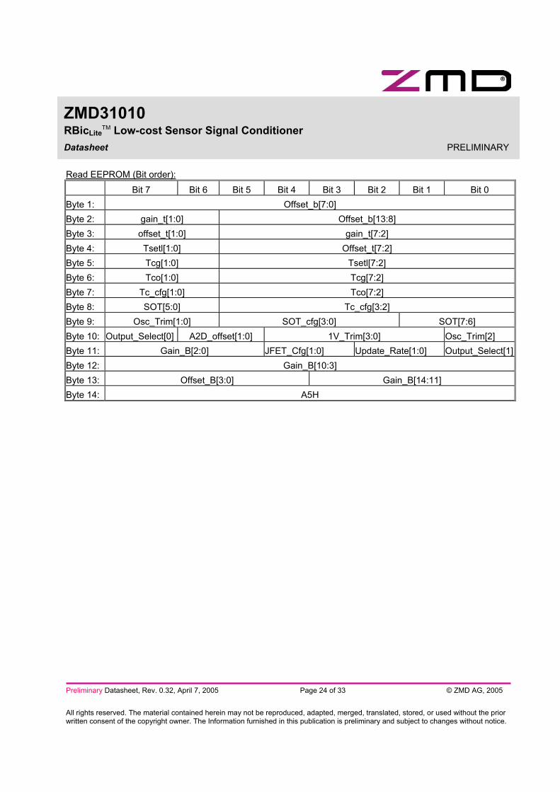
2.7 Read of EEPROM Contents The contents of the entire EEPROM memory can be read out using the Read EEPROM Command (00H). This command will cause the IC to output consecutive bytes on the ZAC WireTM. The interpretation of these bytes is given below:
Figure 3.1 -- Ratiometric Voltage Output, Temperature Compensation via Internal Diode.
The optional bridge sink allows a power save modus. The output voltage can be a) 5% to 95% VDD(=Vsupply). b) 0 to 1V analog output is also possible. The absolute voltage output reference is trim able 1V(+/-2mV) in
TM Low-cost Sensor Signal Conditioner Datasheet PRELIMINARY
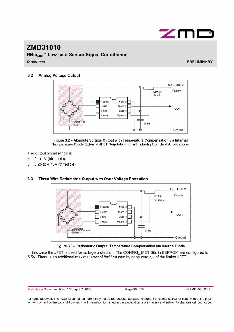
3.2 Analog Voltage Output
Figure 3.2 – Absolute Voltage Output with Temperature Compensation via Internal Temperature Diode External JFET Regulation for all Industry Standard Applications
The output signal range is a) 0 to 1V (trim-able). b) 0.25 to 4.75V (trim-able)
3.3 Three-Wire Ratiometric Output with Over-Voltage Protection
Figure 3.3 – Ratiometric Output, Temperature Compensation via Internal Diode
In this case the JFET is used for voltage protection. The CONFIG_JFET Bits in EEPROM are configured to 5.5V. There is an additional maximal error of 8mV caused by none zero rON of the limiter JFET.
TM Low-cost Sensor Signal Conditioner Datasheet PRELIMINARY
3.4 Digital Output For all three circuits the output signal can also be digital. Depending from the output select bits bridge signal or the bridge signal and temperature signal are sent. For the digital output no load resistor or load capacity are necessary. The IC output includes a pull up resistor of about 100kΩ. The digital output can easily be read by firmware from a microcontroller and ZMD can provide the customer with software in developing the interface.
4 ESD/Latch-Up-Protection All pins have an ESD Protection of >4000V and a Latch-up protection of ±100mA or of +8V/ –4V (to VSS/VSSA). ESD Protection referred to the human body model is tested with devices in SOP8 packages during product qualification. The ESD test follows the human body model with 1.5kOhm/100pF based on MIL 883, Method 3015.7.
TM Low-cost Sensor Signal Conditioner Datasheet PRELIMINARY
6 IC Characteristics
6.1 Absolute Maximum Ratings PARAMETER SYMBOL MIN TYP MAX UNITS
Analog Supply Voltage VDD -0.3 6.0 V
Voltages at Analog I/O – In Pin VINA -0.3 VDDA+0.3 V
Voltages at Analog I/O – Out Pin VOUTA -0.3 VDDA+0.3 V
Storage Temperature Range TSTOR -50 150 °C
Storage Temperature Range TSTOR<10h -50 170 °C
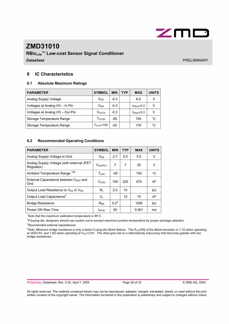
6.2 Recommended Operating Conditions PARAMETER SYMBOL MIN TYP MAX UNITS
Analog Supply Voltage to Gnd VDD 2.7 5.0 5.5 V
Analog Supply Voltage (with external JFET Regulator) VSUPPLY 7 7 30 V
Ambient Temperature Range 1&2 Tamb -50 150 °C
External Capacitance between VDDA and Gnd CVDD 100 220 470 nF
Output Load Resistance to VSS or VDD RL 2.5 10 kΩ
Output Load Capacitance3 CL 10 15 nF
Bridge Resistance RBR 0.24 100k kΩ
Power ON Rise Time trPON 50 0.001 ms 1Note that the maximum calibration temperature is 85°C. 2If buying die, designers should use caution not to exceed maximum junction temperature by proper package selection. 3Recomended external capacitances. 4Note: Minimum bridge resistance is only a factor if using the Bsink feature. The RDS(ON) of the Bsink transistor is 1.1Ω when operating at VDD=5V, and 1.6Ω when operating at VDD=3.0V. This does give rise to a ratiometricity inaccuracy that becomes greater with low bridge resistances.
TM Low-cost Sensor Signal Conditioner Datasheet PRELIMINARY
6.3 Electrical Parameters PARAMETER SYMBOL CONDITIONS MIN TYP MAX UNITS
SUPPLY VOLTAGE / REGULATION
Supply Voltage VDD 2.7 5.0 5.5 V
Supply Current (varies with update rate and output mode)
IDD 150 500 1500 µΑ
Temperature Coefficient – PTAT Source TCPTAT 20 100 ppm/K*
Power Supply Rejection Ratio PSRR 60 dB*
Power-On Clear Level POR 1.4 2.6 V
ANALOG TO DIGITAL CONVERTER (ADC)
Resolution RES 14 Bit
Integral Nonlinearity (INL) INL Charge balancing -4 +4 LSB1
Differential Nonlinearity (DNL) DNL Based on ideal slope -1 +1 LSB*
Response Time TRES Varies with update rate. Value given at fastest rate.
1 ms
ANALOG OUTPUT PARAMETERS (DAC + BUFFER)
Max. Output Current IOUT Max current maintaining accuracy 2.2 mA
Resolution Res Referenced to VDD 11 Bit
Absolute Error EABS DAC input to output -10 +10 mV
Differential Nonlinearity DNL No missing codes -1.5 +1.5 LSB11Bit*
Upper Output Voltage Limit VOUT 95% VDD
Lower Output Voltage Limit VOUT @2.5KΩ pull down ,0-1V output 1 mV
ZACwire™
Serial Interface*
Pull-Up Resistor Master RZAC,PU On-chip pull-up resistor switched on during digital output mode and during “command listen” mode (first 6ms after power up)
TM Low-cost Sensor Signal Conditioner Datasheet PRELIMINARY
PARAMETER SYMBOL CONDITIONS MIN TYP MAX UNITS
TOTAL SYSTEM
Start-Up-Time tS Power-up to output 10 ms
Response Time tR Update_rate=<1ms 1 2 ms
Sampling Rate fS Update_rate=<1ms 1000 Hz
Supply Current IDD Update_rate=<1ms 1 mA
Overall Linearity Error ELIND Bridge input to output -- Digital 0.02 TBD %
Overall Linearity Error ELINA Bridge input to output -- Analog 0.1 TBD
Overall Ratiometricity Error ER Not using Bsink feature 0.035 TBD %
Overall Absolute Error E Bridge input to output TBD % 1 Note this is +/- 4 LSBs to the 14-bit A-to-D conversion. This implies absolute accuracy to 12-bits on the A-to-D result. Non-linearity is typically better at temperatures less than 125°C. * The parameters with an * under “Units” are tested by design.
6.4 Analog Inputs RBic LiteTM incorporates an extended 14-bit charge-balanced ADC which allows for a single gain setting on the Pre-Amplifier to handle bridge sensitivities from 1.2 - 36mV/V while maintaining 8-12 bits of output resolution. The table below illustrates the minimum resolution achievable for a variety of bridge sensitivities.
6.5 Temperature Compensation and Temperature Output A highly-linear Bandgap/PTAT circuit is used in order to produce a signal which can be used in compensation of the bridge over temperature. In addition, when digital mode is activated both bridge and temperature signals (8-bit temperature quantity) can be broadcast on the ZACwireTM pin.
TM Low-cost Sensor Signal Conditioner Datasheet PRELIMINARY
6.6 High Voltage Operation A linear regulator control circuit is included on the IC to interface with an external JFET to allow for operation in systems where the supply voltage exceeds 5.5V. This circuit can also be used for over-voltage protection. The regulator set point has a coarse adjust (EEPROM bit) that can adjust the set point around 5.0 or 5.5V. In addition, the 1V trim will also act as a fine adjust for the regulation set point. Note: If using the external JFET for over-voltage protection purposes (i.e., 5V at JFET drain and expecting 5V at JFET source), there will be a voltage drop across the JFET, thus ratiometricity will be compromised somewhat depending on the rds(on) of the chosen JFET. A Vishay J107 is the best choice that would produce only an 8mV drop worst case. If using as regulation instead of over-voltage, a MMBF4392 also works well.
7 Test The test program is based on this datasheet. The final parameters which will be tested during series production are listed in the tables of section 6.3. The digital part of the IC includes a scan path, which can be activated and controlled during wafer test. It guarantees failure coverage more than 98%. Further test support for testing of the analog parts on wafer level is included in the DSP.
8 Reliability A reliability investigation according to the in-house non-automotive standard will be performed.
9 Customization For high-volume applications, which require an up- or downgraded functionality compared to the ZM31010, ZMD can customize the circuit design by adding or removing certain functional blocks. For it ZMD has a considerable library of sensor-dedicated circuitry blocks. Thus ZMD can provide a custom solution quickly. Please contact ZMD for further information.
10 Related Documents ZMD31010 RBicLite
TM Evaluation Kit Documentation For the most recent revisions of this document and of the related documents please go to www.zmd.biz.
TM Low-cost Sensor Signal Conditioner Datasheet PRELIMINARY
This information applies to a product under development. Its characteristics and specifications are subject to change without notice. ZMD assumes no obligation regarding future manufacture unless otherwise agreed in writing. The information furnished hereby is believed to be correct and accurate. However, ZMD shall not be liable to any customer, licensee or any other third party for any damages in connection with or arising out of the furnishing, performance or use of this technical data. No obligation or liability to any customer, licensee or any other third party shall result from ZMD’s rendering of technical or other services.