154
Copyright by Vladimir Mancevski 2011

Copyright
by
Vladimir Mancevski
2011
The Disser tation Committee for Vladimir Mancevski Cer tifies that this is the approved version of the following disser tation:
FABRICATION AND ANALYSIS OF
CARBON NANOTUBE BASED EMITTERS
Committee:
John Markert, Supervisor
Zhen Yao
Chih-Kang Shih
Qian Niu
Benito Fernandez

FABRICATION AND ANALYSIS OF
CARBON NANOTUBE BASED EMITTERS
by
Vladimir Mancevski, B.S.M.E., M.S.E.
Disser tation
Presented to the Faculty of the Graduate School of
The University of Texas at Austin
in Partial Fulfillment
of the Requirements
for the Degree of
Doctor of Philosophy
The University of Texas at Austin
August 2011

Dedication
This Dissertation is dedicated to my wife Teresa and my son Alex for believing in me and
in my science and encouraging me to continue pursuing my dreams; to my father
Aleksandar for his advice that I can do anything if I put my mind and effort to do it, to
my mother Olivera who always encourages me to stay happy and positive; and to my
American parents, Jack and Laura, who have been my leadership models and who have
always been there for me.

v
Acknowledgements
I thank my colleague Paul McClure from Xidex for reading and editing every
single research work done and every report that I have written, and checking this
dissertation for logic and language. I also thank him for his helpful suggestions on the
direction of the research I have conducted and for the analysis he did on the size of the
light spots from the field emitters.
I thank Ryan Williams for spending numerous hours of work with me on the SEM
and FIB tools, preparing field emitters and conducting experiments. His exceptional
skills in SEM and FIB made many of the research ideas become practical. His ion
milling work made the perfect base for emitters. I thank him for traveling with me to
California to conduct the cool experiment on operating an SEM with a CNT emitter.
I thank Leonid Karpov from Xidex for the great and insightful suggestions on
how to make a perfect field emission experiment and for his help in conducting some of
the experiments. We have spent many hours discussing and interpreting the field
emission results. I thank him for the great MEMS ideas on how to fabricate the emitter
arrays.
I thank Philip Rack from The University of Tennessee at Knoxville and ORNL
for his guidance in setting up and conducting the CNT editing experiments. I thank him
for the numerous telephone and email discussions on how to interpret the results and in
understanding the gas injection models they have developed. I also thank his student
Matthew Lassiter for conducting the first set of water etching experiments at their SEM,
and for performing the models of the localized pressure and etch rates.
I thank John Markert for being so patient with me over an extended period of time
and for his encouragement to continue working on my Ph.D. degree while working at

vi
Xidex. I thank him for the guidance in many of my experiments. I thank him for always
having time to talk to me when I would drop by his office, even if not being scheduled;
most of them not being scheduled. I thank him for helping me edit and prepare this
Dissertation.
I thank Keith Stevenson from the Department of Chemistry and Biochemistry for
his helpful advice with making and testing the field emitters. I thank Earl Weltmer from
ScanService Corporation for letting us use his SEM as a test platform for the CNT
emitters. I thank David Joy at the University of Tennessee at Knoxville and ORNL for
providing support related to emitter design and interpretation of test results. I thank
Victor Vartanian and John Allgair from International SEMATECH Manufacturing
Initiative (ISMI) for funding the work on CNT electrical conductivity. I also thank Hal
Bogardus for sponsoring early work done for SEMATECH and for encouragement in
pursuing the work further. I thank Yong Lee for the initial information on how to build a
nanomanipulator. I thank Boris Begus for the CAD designs of the nanomanipulator and
the field emission rig.
Finally, I thank my wife Teresa and my son Alex for being patient with me when
I had to juggle work and graduate work and for believing that I can do both. I thank them
for their continuous support in everything I decide to do.
The research work presented here was partially funded by DOE grant number DE-
FG02-06ER84408 and NSF grant number IIP-0712036.
vii
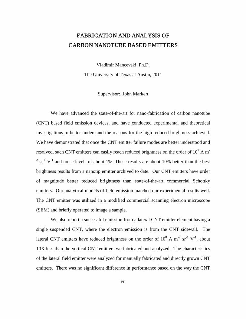
FABRICATION AND ANALYSIS OF
CARBON NANOTUBE BASED EMITTERS
Vladimir Mancevski, Ph.D.
The University of Texas at Austin, 2011
Supervisor: John Markert
We have advanced the state-of-the-art for nano-fabrication of carbon nanotube
(CNT) based field emission devices, and have conducted experimental and theoretical
investigations to better understand the reasons for the high reduced brightness achieved.
We have demonstrated that once the CNT emitter failure modes are better understood and
resolved, such CNT emitters can easily reach reduced brightness on the order of 109 A m-
2 sr-1 V-1 and noise levels of about 1%. These results are about 10% better than the best
brightness results from a nanotip emitter archived to date. Our CNT emitters have order
of magnitude better reduced brightness than state-of-the-art commercial Schottky
emitters. Our analytical models of field emission matched our experimental results well.
The CNT emitter was utilized in a modified commercial scanning electron microscope
(SEM) and briefly operated to image a sample.
We also report a successful emission from a lateral CNT emitter element having a
single suspended CNT, where the electron emission is from the CNT sidewall. The
lateral CNT emitters have reduced brightness on the order of 108 A m-2 sr-1 V-1, about
10X less than the vertical CNT emitters we fabricated and analyzed. The characteristics
of the lateral field emitter were analyzed for manually fabricated and directly grown CNT
emitters. There was no significant difference in performance based on the way the CNT
viii
emitter was fabricated. We showed that the fabrication technique for making a single
CNT emitter element can be scaled to an array of elements, with potential density of 106-
107 CNT emitters per cm2.
We also report a new localized, site selective technique for editing carbon
nanotubes using water vapor and a focused electron beam. We have demonstrated the
use of this technique to cut CNTs to length with 10s of nanometers precision and to etch
selected areas from CNTs with 10s of nanometers precision. The use of this technique
was demonstrated by editing a lateral CNT emitter. We have conducted investigations to
demonstrate the effects of higher local water pressure on the CNT etching efficiency.
This was achieved by developing a new method of localized gas delivery with a nano-
manipulator.

ix
Table of Contents
List of Tables .................................................................................................................... xii
List of Figures .................................................................................................................. xiii
Chapter 1: Introduction .....................................................................................................1
Chapter 2: Theoretical Models of Carbon Nanotube Based Emitters ..............................4
2.1 Electron Emission Overview .................................................................4
2.2 CNT Field Emission Model Analysis ....................................................5
2.3 Model Verification with Experimental Results ...................................12
Chapter 3: Instrumentation and Components .................................................................15
3.1 Scanning Electron Microscope (SEM) ................................................15
3.2 In-Situ Nanomanipulator .....................................................................18
3.3 Gas Injection System ...........................................................................20
3.4 Field Emission Evaluation Hardware ..................................................23
Chapter 4: Carbon Nanotube Field Emitters as Sources for Scanning Electron Microscopes ..................................................................................................25
4.1 Introduction ..........................................................................................25
4.1.1 Conventional Cold Field Emitters ...........................................26
4.1.2 Nanotip Emitters ......................................................................27
4.1.3 Emitter Brightness ...................................................................28
4.1.4 Emitter Stability and Lifetime .................................................29
4.1.5 Other Field Emitter Figures of Merit .......................................30
4.2 Fabrication ...........................................................................................32
4.2.1 Fabrication of Carbon Nanotube Field Emitters ......................32
4.2.2 Manual Mounting.....................................................................32
4.2.3 Direct CNT Growth .................................................................35
4.2.4 Competing Nanotube Tip Fabrication Processes .....................36
4.2.5 Emitter Fabrication Improvements ..........................................38
4.2.6 Field Emission Testing Hardware ............................................38
4.3 Experimental Results ...........................................................................39

x
4.3.1 Measurement and Evaluation of CNT Emitters .......................39
4.3.2 Testing of the CNT emitter in an SEM instrument ..................47
4.4 Conclusions ..........................................................................................49
4.4.1 Emitter Design .........................................................................49
4.4.2 CNT Emitter Fabrication .........................................................50
4.4.3 Summary ..................................................................................52
4.5 Future Research ...................................................................................54
4.5.1 Emitter Energy Spread Measurement ......................................54
4.5.2 Virtual Source Measurements ..................................................55
Chapter 5: Lateral Carbon Nanotube Field Emitters ......................................................56
5.1 Introduction ..........................................................................................56
5.1.1 Related Work ...........................................................................58
5.2 Experimental Results ...........................................................................61
5.2.1 CNT Lateral Emitter Substrate Fabrication .............................61
5.2.2 Manual CNT Lateral Emitter Fabrication ................................62
5.2.3 CNT Lateral Emitter Fabrication with Direct CNT Growth ....64
5.2.4 Evaluation of the CNT Lateral Emitter ....................................65
5.3 Lateral Arrays ......................................................................................68
5.3.1 Scaleable Fabrication of Lateral CNT Emitters .......................69
Chapter 6: Site Selective Carbon Nanotube Editing.......................................................74
6.1 Introduction ..........................................................................................74
6.1.1 Motivation for Carbon Nanotube Editing ................................75
6.1.2 Summary of Previous Carbon Nanotube Editing Techniques .76
6.1.3 Mechanistic and Quantitative Description ...............................78
6.2 Experimental Section ...........................................................................81
6.2.1 Experimental Setup I................................................................81
6.2.1.1 Samples .....................................................................82
6.2.1.2 Demonstration of the CNT cutting process ..............82
6.2.1.3 Study of the CNT Etching Parameters ......................87
6.2.1.4 CNT Area Etching ....................................................93
6.2.2 Experimental Setup II ..............................................................95

xi
6.2.2.1 Demonstration of improved CNT cutting efficiency 95
6.2.2.2 Experimental Setup II ...............................................96
6.2.2.3 Relationship between the nozzle-sample distance and the localized precursor pressure ................................98
6.2.2.4 Cantilevered CNT Etching ......................................105
6.2.2.5 Application of the CNT Etching on a Field Emission Device .....................................................................107
6.2.2.6 Modeling of the CNT Cutting Process....................109
6.3 Summary and conclusions .................................................................111
Appendices .....................................................................................................................115
Appendix A: Manual Fabrication of a Carbon Nanotube Tip ...............115
A1 Introduction ......................................................................115
A2 Sample Preparation ..........................................................116
A3 Picking Up a CNT with the W Tip ..................................117
A4 Separating the CNT from the CNT Source ......................118
A5 Attaching the CNT to the AFM Tip .................................119
A6 Cutting the CNT Away from the W tip ...........................120
A7 Alternative Procedures .....................................................121
Appendix B: Evaluating the Contact Resistance between Carbon Nanotubes and W and Si Probe Tips ...............................122
B1 Introduction ......................................................................122
B2 Experiments and Evaluation Procedures .........................122
B3 Conclusions ......................................................................128
References ..................................................................................................................129
Vita ..................................................................................................................135

xii
List of Tables
Table 2.1: Experimental parameters extracted from the Fowler-Nordheim plot for three different nanotips.........................................................................13
Table 2.2: Computed field emitter parameters for three different nanotips ................13
Table 4.1: Summary of the competing state-of-the-art emitter technologies..............31
Table 4.2: Summary of the figures-of-merit for Emitter #1 which for varying currents levels ............................................................................................44
Table 4.3: Summary of the figures-of-merit for Emitter #2 which was tested at varying tip-to-anode distances ...............................................................44
Table 4.4: Evaluation of set of 21 CNT emitters ........................................................50
Table 4.5: Summary of the best two CNT emitters ....................................................53
Table 5.1: Comparison between a vertical field emitter and a lateral field emitter. .......................................................................................................67
Table 6.1: Summary of the investigated beam energies, currents, and SEM settings .....................................................................................................102
Table 6.2: Summary of the experimental results measuring etch rate as function of the nozzle sample distance. ...................................................103

xiii
List of Figures
Figure 2.1: Illustration of the potential barrier of a metal surface with respect to a vacuum level. The barrier can be lowered by applying temperature as in thermionic emission, applying high electric field as in field emission, and applying both as in Schottky emission. ................5
Figure 2.2: Schematic drawing of a CNT emitter experiment with key parameters annotated. ..................................................................................7
Figure 2.3: Models of virtual source for carbon nanotube emitters. (a) virtual source rv for a CNT with hemispherical cup, (b) with flat cup, and (c) with open cup. Reprinted from N. de Jonge [2.5] ...............................11
Figure 2.4: I-V plots of three nanotip field emitters, CNT, Pt, and Si. The anode-cathode gap was 60 µm. ..................................................................12
Figure 2.5: Fowler-Nordheim plot and a linear fit for CNT nanotip, Pt nanotip, and Si tip. ...................................................................................................12
Figure 3.1: Hitachi S-4000 SEM used for conducting the CNT editing experiments and for fabricating CNT emitters. .........................................16
Figure 3.2: Hitachi S-4300SE/N SEM and customized gas injection system. .............16
Figure 3.3b: A commercial NanoBot® nanomanipulator, currently manufactured by Xidex Corp. that is based on the prototype from Figure 3.3a. ..............19
Figure 3.3a: A custom 3-axis nanomanipulator that was designed and build for the purposes of conducting the experiments presented in our research. .....................................................................................................19
Figure 3.4: The principle of operation of an inertial linear stage .................................20
Figure 3.5: Photographs of a) the gas injection flange, b) the gas delivery needle, and c) an SEM micrograph of the delivery needle in close proximity to the substrate...........................................................................21
Figure 3.6: Schematic of a gas injection system with a nozzle attached to a nanomanipulator for precise nozzle positioning. Option 2# has the gas reservoir inside the chamber. ...............................................................21
Figure 3.7: Prototype gas delivery system with a nozzle on a nanomanipulator and with in-situ gas-liquid bottle. Insert shows the end of the needle ~200 µm from the sample...............................................................22

xiv
Figure 3.8: The field emission test chamber with viewport. As an example, inside the chamber is an array of CNT emitters with tip to tip spacing of about 270 µm. The bright spots are due to the electrons hitting a phosphor coated ITO glass. .........................................................24
Figure 4.1a: CNT emitter grown directly on Si tip ........................................................32
Figure 4.1c: CNT emitter manually mounted on a sharpened W tip .............................32
Figure 4.1b: CNT emitter manually mounted on a Si tip ...............................................32
Figure 4.2: Illustration of focused ion beam assisted carbon nanotube alignment. a) CNT before alignment, b) CNT after alignment..................34
Figure 4.3: Examples of a) electrochemically sharpened W tip, and b) focused ion beam sharpened W tip..........................................................................35
Figure 4.4: Gallery of carbon nanotube tips grown directly on silicon SPM tips. Average CNT diameter is ~ 10 nm. ..................................................36
Figure 4.5: Field emission testing rig. ..........................................................................39
Figure 4.6: Holder for testing CNT emitters on W wire ..............................................39
Figure 4.7: a) The image of the field emission pattern digitally recorded with a camera, where its radius was determined with intensity analysis (in this example R was 87 µm for a gap of 408 µm), b) normalized intensity plot, c) normalized contour plot. .................................................40
Figure 4.8: Field emission as recorded during brightness measurements for Emitter #1. Legend: (average current/extraction voltage/current noise/gap) ...................................................................................................41
Figure 4.9: Field emission (average of 2 or 3 runs) as recorded during brightness measurements for Emitter #2. Legend: (average current/extraction voltage/current noise/gap) ............................................42
Figure 4.10: Data for Emitter #1 tests, a) average of 16 measured I-V curves and the computed fit for the high current regime, b) corresponding Fowler-Nordheim plot and the computed linear fit for the high current regime. ...........................................................................................43
Figure 4.11: Data for Emitter #2 tests, a) average of N measured I-V curves (N = 40 for Gap = 296 µm, N = 26 for Gap = 414 µm, N = 26 for Gap = 611 µm) and the computed fits for the high current regime, b) Fowler-Nordheim plots and the computed linear fits for the high current regime. ...........................................................................................44

xv
Figure 4.12: Correction of an I-V curve with a 500 kΩ ballast resistor in series with the CNT emitter array to match an I-V curve with 0 kΩ ballast resistor. The CNT emitter array in this example had Imax = 420 µA. ......................................................................................................46
Figure 4.13: 10 hours time test for two CNT emitters: a) CNT grown on Si, I = 3 µm, Inoise = 50 nA or 1.7% b) CNT mounted on W, I = 1 µm, Inoise = 47 nA or 4.9% .................................................................................47
Figure 4.14: SEM filament holder for CNT emitter, a) holder used in initial trials, b) CAD model of the new holder design .........................................47
Figure 4.15: I-V curves of 2 CNT emitters as operated in the SEM ..............................49
Figure 4.16: Time and stability test of CNT emitter #1 during brief SEM operation. Noise level is 4.4% for the last 2.5 min and 19.4% for the entire range. ..........................................................................................49
Figure 4.17: a) CNT emitter that was mounted to a W tip and was Pt welded at the base, L ~ 1100 nm, b) the same CNT emitter was shortened after some emission tests, L ~ 400 nm. ......................................................52
Figure 4.18: A camera photo of an SEM screen, demonstrating a proof-of-concept of operating an SEM instrument with a CNT emitter. .................53
Figure 5.1: Schematic drawing of lateral CNT emitter design and ranges of the key dimensions...........................................................................................61
Figure 5.2: (a) Pt pillars on the apex of a sharp Si tip, fabricated using e-beam induced deposition technique. (b) Ion-milled W to produce knife-edge pillars for growing or mounting CNT emitters. ................................62
Figure 5.3: (a) Manually attached CNT emitter on an ion-milled W tip. (b) The CNT was welded with W using e-beam deposition. Close-up view of the attachment between the CNT and the W edge. (c) TEM image of typical CNT as the one attached in (a). .......................................63
Figure 5.4: Examples of three lateral-emission CNT emitters. The Si substrate was ion-milled to fabricate a gap. The CNTs were grown directly using CVD process. Few extra CNTs in the gap were removed for sample (a) and (b). Sample (c) grew only a single CNT. .........................65
Figure 5.5: a) The image of the field emission pattern from a lateral emitter, digitally recorded with a camera, where its radius was determined with intensity analysis (in this example the semi-axes of the spot were 193 µm for X and 254 µm for Y for a gap of 596 µm), b) normalized intensity plot, c) normalized contour plot. ..............................67

xvi
Figure 5.6: Long time stability and noise test for (a) Si and W based vertical CNT emitters and (b) Si based lateral field emitter. ..................................68
Figure 5.7: Lateral CNTs grown directly with a thermal CVD process on Si posts. The CNT had 10 nm diameter and the same length as the post spacing, ~2 µm. ..................................................................................69
Figure 5.8: Lateral CNTs grown directly on an array of sharp Si posts, suspended from the tops of the Si posts. The white arrows were added to point to the suspended CNTs. .....................................................71
Figure 5.9: Example of micro-fabrication of an array of Si posts ................................72
Figure 6.1: Manufacturing situations where repair is needed to make a useful CNT AFM tip .............................................................................................75
Figure 6.2: Examples of manufacturing of CNT interconnects in need of repair. Arrows indicate CNTs that need to be removed. Boxes indicate potential area that could be cleaned to produce better interconnects. Sample a) was fabricated by the author and sample b) is a network of suspended SWCNTs published by Franklin et al. [6.10] ..........................................................................................................76
Figure 6.3: Schematic showing a) the substrate and precursor gas without an electron beam, b) a focused electron beam stimulated deposition process, and c) a focused electron beam stimulated etch process. .............79
Figure 6.4: Secondary electron imaging example during line scanning across a CNT (top) and after CNT is cut (bottom) ..................................................83
Figure 6.5: Example of carbon nanotube cutting using a box scan. .............................84
Figure 6.6: The CNTs in image a-b) were etched using a line scan, and the CNTs in image c-d) were cut in a box scan. ..............................................84
Figure 6.7: Relationship between time to cut and the initial diameter of the CNT............................................................................................................85
Figure 6.8: Progression of line scanning secondary electron image towards end point ...........................................................................................................86
Figure 6.9: The CNT was imaged by the SEM scanning the region highlighted by the dotted red line. There was significant deposition on the CNT due to carbon contamination in the SEM chamber deposited during exposure to the electron-beam. .......................................................87
Figure 6.10: Deposition rate, etching rate, and net rate versus increasing electron flux ...............................................................................................89

xvii
Figure 6.11: Deposition rate, etching rate, and net rate versus increasing electron flux ...............................................................................................89
Figure 6.12: RF plasma cleaning time vs. net etching/deposition experiment ...............91
Figure 6.13: CNT etch rate versus beam current ............................................................92
Figure 6.14: Main effect plot from full factorial DOE ...................................................93
Figure 6.15: 1.5 µm x 0.75 µm area CNT etching with water vapor precursor. It is clear that the etching using water vapor cleaned an entire microns-scale area of its carbon nanotubes without modifying the neighboring nanotubes. ..............................................................................94
Figure 6.16: Before (left) and after (right) area cleaning ...............................................94
Figure 6.17: Electron beam induced etching system with novel nanomanipulator based gas delivery/injection system. ..........................................................98
Figure 6.18: Visualization of the water vapor flow from the nozzle as the nozzle-sample gap was reduced. The gas spread angle β is estimated from the streamlines. ...............................................................100
Figure 6.19: Selectively cutting a CNT at low sample currents (10−80 pA), before (a) and after (b). Note that the large CNT to the left and the CNT to the right are only partially cut. ....................................................101
Figure 6.20: Selectively cutting a CNT at low sample currents (10−80 pA), before (a) and after (b). Note that the CNT to the left is only partially cut. .............................................................................................101
Figure 6.21: Partial (non complete) cutting of a 90 nm diameter CNT, before (a), after 14 minutes of etching (b), and a split in the CNT diameter due to the partial cutting (c). ....................................................................102
Figure 6.22: Demonstration of gas delivery system fixed to a nanomanipulator that allows precise positioning of the gas nozzle to the sample with a rage of 50 μm to 1 mm and more. The resulting nozzle proximity results in improved CNT etching capabilities. ........................104
Figure 6.23: Demonstration of improved CNT etching time (etching rate) vs. nozzle-sample distance. ...........................................................................105
Figure 6.24: Probe current vs. nozzle-sample distance. ...............................................105
Figure 6.25: (a) shows two free standing CNTs with different diameter. After an initial etching attempt the thinner CNT was completely etched away while the thicker CNT was unchanged (b). After some additional etching time the thicker CNT was bent and deformed but it was not cut (c).................................................................................106

xviii
Figure 6.26: A free standing CNT, before (a) and after its length was shortened (b) using localized CNT cutting. ..............................................................107
Figure 6.27: Example of a lateral (horizontal) CNT device fabricated by Xidex for use as a lateral field emitter ................................................................108
Figure 6.28: An excess CNT strung from a silicon post (viewed top down) and the surface, before (left) and after (right) it was removed using selective CNT etching. .............................................................................108
Figure 6.29: Effect of pressure on the etching rate ......................................................110
Figure A2: A NanoBot Model NX-2000 mounted on the door assembly of an SEM. ........................................................................................................116
Figure A1: CNT manually attached to a Si AFM tip. ................................................116
Figure A4: Mounting of a sharp W tip on the NanoBot end effector. .......................117
Figure A3: AFM tip and CNT source ........................................................................117
Figure A6: W tip maneuvered to within a few µm of a CNT. ...................................118
Figure A5: W tip approaching CNT source. ..............................................................118
Figure A7: W tip in contact with the selected CNT. ..................................................119
Figure A8: CNT separated from substrate using current pulse. .................................119
Figure A10: CNT placed along the side of the AFM tip. .............................................120
Figure A9: W tip carrying CNT translated to within a few µm of the AFM tip. ......120
Figure A11: CNT separated from the W tip. ................................................................121
Figure B1: Electrical characterization of W tip to a CNT nanowire grown on Si. a) SEM image of the physical connection, b) I-V curves from the electrical measurement. ......................................................................123
Figure B2: Electrical characterization of W tip to a CNT tip manually attached to the W and the Si tip. a) SEM image of the physical connection, b) I-V curves from the electrical measurement. .......................................124
Figure B3: Electrical characterization of CNT manually attached to two W tips. a) SEM image of the physical connection, b) I-V curves from the electrical measurement. ......................................................................125
Figure B4: I-V results showing the effect of Pt welding (via electron induced precursor deposition) on electrical characteristics of a W-CNT-W connection. a) I-V curves for Sample 1 and b) for Sample 2. ..................126
Figure B5: Comparative results showing the electrical characteristics of a W-CNT-W connection before (legend 3 and 1) and after Pt welding (legend 6 and 11). a) I-V curves for Sample 1 and b) for Sample 2. .......127

xix
Figure B6: Minimum resistivity of a W-CNT contact dropped after the CNT was welded to the W with Pt. ...................................................................127

1
Chapter 1: Introduction
The main subjects of research presented here are carbon nanotube (CNT) based
devices, and in particular, carbon nanotube based field emitters. We have focused our
research on discovering new fabrication methods for making CNT based devices and
have analyzed their properties and figures of merit. We also present new tools that were
developed in order to fabricate and/or analyze the CNT devices. Although our methods
and devices were demonstrated with carbon nanotubes, the findings are applicable to
other nanomaterials and nanodevices.
In this presentation we have dedicated a Chapter to each of the following related
subjects: carbon nanotubes field emitters as sources for scanning electron microscopes,
lateral nanotubes field emitters, and site selective carbon nanotube editing.
In Chapter 2 we present theoretical models for field emission from a carbon
nanotube tip. We showed that the operation of the CNT emitter can be theoretically
predicted by the Fowler–Nordheim equation in its simplified form. We verified the CNT
field emission model with experimental data and found that the model fits well for a CNT
nanotip and a similar Pt nanotip, both with 10s of nanometers diameter and a cylindrical
shank. Chapters 4 and 5 of this work will use the above derived equations to demonstrate
and analyze field emission from a CNT emitter.
In Chapter 3 we review the equipment and the components that were used,
modified, and/or developed for the investigation conducted in Chapters 4 to 6. The
instruments used for this work include a Scanning Electron Microscope (SEM), a
nanomanipulator, a gas injection system, and a field emission testing vacuum chamber.
SEMs are primarily used as imaging tools that allow viewing of nanometer sized objects
and materials. There is a new trend in nanotechnology to use the SEM instrument as
nanofabrication tool. Being on the forefront of this trend, we have developed a new type
of nanomanipulator that was used to fabricate and investigate the CNT emitters, as

2
described in Chapters 4 and 5. We also developed a new type of gas injection system that
was used to improve the fabrication of the CNT emitters reported in Chapters 4 and 5.
The emission testing vacuum chamber was built to help us investigate the CNT emitters.
In Chapter 4 we report on the experimental and theoretical investigations to better
understand how to achieve CNT emitters with high reduced brightness, on the order of
109 A m-2 sr-1 V-1, and noise levels of about 1%. We developed two fabrication methods
for making CNT emitters using: manual mounting of carbon nanotubes and direct carbon
nanotube growth. During this work we made and tested more than 40 different CNT
emitters, either grown or mounted, and analyzed 27 CNT emitters. We investigated the
failure mechanisms and found ways to improve the operation of the field emitter. As a
result of the findings we advanced the state-of-the-art for nano-fabrication of CNT based
field emission devices. A few CNT emitters were utilized in a modified commercial
SEM and briefly operated to image a sample. Therefore, we demonstrated the proof-of-
concept of operating an SEM instrument with a CNT emitter.
In Chapter 5 we present a new type of emitter, a lateral CNT emitter element
having a single suspended CNT, where the electron emission is from the CNT sidewall.
The lateral CNT emitters have reduced brightness on the order of 108 A m-2 sr-1 V-1,
about 10X less than the vertical CNT emitters we fabricated and analyzed in Chapter 4.
However, the lateral CNT emitters are more suitable for operating in an array
configuration. We showed that the fabrication technique for making a single CNT
emitter element can be scaled to an array of elements, with potential density of 106-107
CNT emitters per cm2. We developed two fabrication methods for making lateral CNT
emitters using: manual mounting of carbon nanotubes and direct CNT growth. There was
no significant difference in performance based on the way the CNT emitter was
fabricated. We used the CNT editing methods described in Chapter 6 to modify and
improve a lateral CNT emitter that was fabricated with a direct growth method described
in Chapter 5.

3
In Chapter 6 we report a new localized, site selective technique for editing CNTs
using water vapor and a focused electron beam. We investigated the relevant electron
beam parameters (beam current and the beam energy) and determined their role in the
electron beam-based CNT etching process. We also investigated the gas precursor
parameters (localized precursor pressure, precursor flux, and precursor sample chemistry)
and understood their role to the chemistry and physics of the carbon nanotube etching.
We have conducted investigations to demonstrate the effects of higher local water
pressure on the CNT etching efficiency. This was achieved by developing a new method
of localized gas delivery with a nano-manipulator. As a result of these findings we have
advanced the state-of-the-art of electron beam induced etching of carbon nanotubes.
Finally, we have demonstrated the use of this technique to cut CNTs to length with 10s of
nanometers precision and to etch selected areas from CNTs with 10s of nanometers
precision.

4
Chapter 2: Theoretical Models of Carbon Nanotube Based Emitters
2.1 ELECTRON EMISSION OVERVIEW
Electron emission from the surface of a metal can occur due to thermionic
emission, field emission, and Schottky emission, as shown in Figure 2.1. In a brief
description we note that for thermionic emission to occur the material needs to be heated
so as to give the electrons sufficient energy to overcome the potential barrier of the
material. The potential barrier is known as work function ϕ. The physics of thermionic
emission follows Richardson’s Law in terms of the current density (J) from the source to
the operating temperature (T).
The field emission process can be understood as follows. The metal can be
considered a potential box, filled with electrons to the Fermi level, which lies below the
vacuum level. The distance from Fermi to vacuum level is called the work function, ϕ.
The vacuum level represents the potential energy of an electron at rest outside the metal,
in the absence of an external field. In the presence of an electric field E the potential
outside the metal will be deformed along a diagonal line so that a triangular barrier is
formed, through which electrons can tunnel. Most of the emission will occur from the
vicinity of the Fermi level where the barrier is thinnest. Since the electron distribution in
the metal is not strongly temperature-dependent, field emission is only weakly
temperature-dependent and would occur even at the absolute zero of temperature.

5
Figure 2.1: Illustration of the potential barrier of a metal surface with respect to a vacuum level. The barrier can be lowered by applying temperature as in thermionic emission, applying high electric field as in field emission, and applying both as in Schottky emission.
2.2 CNT FIELD EMISSION MODEL ANALYSIS
The carbon nanotube (CNT) based electron emitter is a field emitter which is
operated by applying a strong electric field between the nanotube cathode and an anode
separated some distance away from the cathode. The operation of the CNT emitter can
be theoretically predicted by the Fowler–Nordheim theory [2.1, 2.2] which describes the
field emission process in terms of a tunneling current through the potential barrier
between a metal surface and a vacuum under influence of a strong electrical field.
The current density J, drawn from a point by field emission, for the one-
dimensional Fowler–Nordheim case of a cold metallic planar emitter with parallel planar
anode is known to be [2.2, 2.3]:
𝐽𝐽 = 𝐼𝐼𝑆𝑆
= 𝑐𝑐1𝜙𝜙𝜙𝜙 (𝑦𝑦)𝐹𝐹
2𝑒𝑒𝑒𝑒𝑒𝑒 − 𝑐𝑐2 𝜙𝜙32 𝑣𝑣(𝑦𝑦)𝐹𝐹
Eq. 2.1
where I is the electrical current flowing from surface S, ϕ is the emitter work
function, F is the applied electric field, ε0 is the permittivity of free space, and where, c1

6
and c2 are expressed in terms of universal constants (electron charge e, electron mass m,
and Plank’s constant h) as:
𝑐𝑐1 = 𝑒𝑒3
8𝜋𝜋ℎ= 1.541 × 10⁻⁶ 𝐴𝐴𝑒𝑒𝐴𝐴
𝐴𝐴2 and 𝑐𝑐2 = 8𝜋𝜋√2𝑚𝑚3𝑒𝑒ℎ
= 6.831 × 10⁹ 𝐴𝐴 𝑚𝑚
𝑒𝑒𝐴𝐴32,
and where t(y) and v(y) are dimensionless functions of y:
𝑦𝑦 = 𝑒𝑒3𝐹𝐹4𝜋𝜋𝜀𝜀0𝜙𝜙2
12.
It has been shown that in the case of a triangular potential barrier the functions
t(y) and v(y) can be approximated to be unity [2.3]. Therefore the simplified Fowler–
Nordheim equation can be expressed as:
𝐽𝐽 = 𝐼𝐼𝑆𝑆
= 𝑐𝑐1𝐹𝐹2
𝜙𝜙𝑒𝑒𝑒𝑒𝑒𝑒 −𝑐𝑐2
𝜙𝜙32
𝐹𝐹 = 1.54 × 10⁻⁶ 𝐹𝐹2
𝜙𝜙𝑒𝑒𝑒𝑒𝑒𝑒 −6.83 × 10⁹ 𝜙𝜙
32
𝐹𝐹 Eq. 2.2
This model of the Fowler–Nordheim equation has been proven to work for field
emission from sharp tips up to temperatures of several hundred °C, after which the other
two emission mechanisms, Schottky emission and thermionic emission, play a role. Saito
et al. [2.4] have noticed that an additional correction may be necessary for the case of
CNTs since the density of states in CNTs is not energy independent around the Fermi
level as it is the case for metals. Nevertheless, experimental results have confirmed that
field emission from CNTs can be described to a first approximation by the simple
Fowler–Nordheim equation (Eq. 2.2), and this is the approximation used here.
We will now review how to compute the field emitter parameters from the
experimental I-V curve and the Fowler–Nordheim equation. The experimental setup is
shown in Figure 2.2.

7
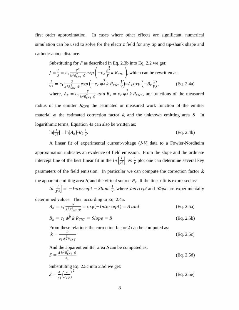
The electric field F at the surface of a free sphere with radius R at potential V is
given by:
𝐹𝐹 = 𝐴𝐴𝑅𝑅 (Eq. 2.3a)
However, in the presence of a tip shank the electric field is reduced, so that the
electric field has to be adjusted by a correction factor k. Therefore, the electric field from
a sharp tip, such as a carbon nanotube with a hemispherical cap of radius RCNT, can be
approximated by as: 𝐹𝐹 = 𝐴𝐴
𝑘𝑘 𝑅𝑅𝐶𝐶𝐶𝐶𝐶𝐶 (Eq. 2.3b)
The experimental value of k for a hemisphere on a thin cylinder has been
estimated to be k = 5. In reality the field strength also depends on the real shape of the
tip, the tip shank, and the cathode-anode distance but in first order approximation of the
field emission phenomena these factors can be neglected. In our analysis we will use this
Figure 2.2: Schematic drawing of a CNT emitter experiment with key parameters annotated.
Camera
I
V
Si or W Shank
+
-
Anode - ITO Glass with Phosphor
Phosphor Spot with Radius Rp
CNT Tip Emitter
Gap d
CNT Radius RCNT
Electron Beam
Beam Spread dΩ
8
first order approximation. In cases where other effects are significant, numerical
simulation can be used to solve for the electric field for any tip and tip-shank shape and
cathode-anode distance.
Substituting for F as described in Eq. 2.3b into Eq. 2.2 we get:
𝐽𝐽 = 𝐼𝐼𝑆𝑆
= 𝑐𝑐1𝐴𝐴2
𝑘𝑘2𝑅𝑅𝐶𝐶𝐶𝐶𝐶𝐶2 𝜙𝜙
𝑒𝑒𝑒𝑒𝑒𝑒 −𝑐𝑐2𝜙𝜙
32
𝐴𝐴𝑘𝑘 𝑅𝑅𝐶𝐶𝐶𝐶𝐶𝐶, which can be rewritten as:
𝐼𝐼𝐴𝐴2 = 𝑐𝑐1
𝑆𝑆𝑘𝑘2𝑅𝑅𝐶𝐶𝐶𝐶𝐶𝐶
2 𝜙𝜙𝑒𝑒𝑒𝑒𝑒𝑒 −𝑐𝑐2 𝜙𝜙
32 𝑘𝑘 𝑅𝑅𝐶𝐶𝐶𝐶𝐶𝐶
1𝐴𝐴=𝐴𝐴𝑘𝑘𝑒𝑒𝑒𝑒𝑒𝑒 −𝐵𝐵𝑘𝑘
1𝐴𝐴, (Eq. 2.4a)
where, 𝐴𝐴𝑘𝑘 = 𝑐𝑐1𝑆𝑆
𝑘𝑘2𝑅𝑅𝐶𝐶𝐶𝐶𝐶𝐶2 𝜙𝜙
𝑎𝑎𝑎𝑎𝑎𝑎 𝐵𝐵𝑘𝑘 = 𝑐𝑐2 𝜙𝜙32 𝑘𝑘 𝑅𝑅𝐶𝐶𝐶𝐶𝐶𝐶 , are functions of the measured
radius of the emitter RCNT, the estimated or measured work function of the emitter
material ϕ, the estimated correction factor k, and the unknown emitting area S. In
logarithmic terms, Equation 4a can also be written as:
ln[ 𝐼𝐼𝐴𝐴2] =ln[𝐴𝐴𝑘𝑘]-𝐵𝐵𝑘𝑘
1𝐴𝐴. (Eq. 2.4b)
A linear fit of experimental current-voltage (I-V) data to a Fowler-Nordheim
approximation indicates an evidence of field emission. From the slope and the ordinate
intercept line of the best linear fit in the 𝑙𝑙𝑎𝑎 𝐼𝐼𝐴𝐴2 𝑣𝑣𝑣𝑣 1
𝐴𝐴 plot one can determine several key
parameters of the field emission. In particular we can compute the correction factor k,
the apparent emitting area S, and the virtual source Rv. If the linear fit is expressed as:
𝑙𝑙𝑎𝑎 𝐼𝐼𝐴𝐴2 = −𝐼𝐼𝑎𝑎𝜙𝜙𝑒𝑒𝐼𝐼𝑐𝑐𝑒𝑒𝑒𝑒𝜙𝜙 − 𝑆𝑆𝑙𝑙𝑆𝑆𝑒𝑒𝑒𝑒 1
𝐴𝐴, where Intercept and Slope are experimentally
determined values. Then according to Eq. 2.4a: 𝐴𝐴𝑘𝑘 = 𝑐𝑐1
𝑆𝑆𝑘𝑘2𝑅𝑅𝐶𝐶𝐶𝐶𝐶𝐶
2 𝜙𝜙= exp(−𝐼𝐼𝑎𝑎𝜙𝜙𝑒𝑒𝐼𝐼𝑐𝑐𝑒𝑒𝑒𝑒𝜙𝜙) =𝐴𝐴 𝑎𝑎𝑎𝑎𝑎𝑎 (Eq. 2.5a)
𝐵𝐵𝑘𝑘 = 𝑐𝑐2 𝜙𝜙32 𝑘𝑘 𝑅𝑅𝐶𝐶𝐶𝐶𝐶𝐶 = 𝑆𝑆𝑙𝑙𝑆𝑆𝑒𝑒𝑒𝑒 = 𝐵𝐵 (Eq. 2.5b)
From these relations the correction factor k can be computed as: 𝑘𝑘 = 𝐵𝐵
𝑐𝑐2 𝜙𝜙32𝑅𝑅𝐶𝐶𝐶𝐶𝐶𝐶
(Eq. 2.5c)
And the apparent emitter area S can be computed as: 𝑆𝑆 = 𝐴𝐴 𝑘𝑘2𝑅𝑅𝐶𝐶𝐶𝐶𝐶𝐶
2 𝜙𝜙𝑐𝑐1
(Eq. 2.5d)
Substituting Eq. 2.5c into 2.5d we get:
𝑆𝑆 = 𝐴𝐴 𝑐𝑐1 𝐵𝐵𝑐𝑐2𝜙𝜙
2 (Eq. 2.5e)

9
where the apparent emitter area S only depends on the I-V coefficients and the
work function ϕ. For an emitter with a circular cross section, like a closed end CNT, the
virtual source Rv can be computed from the apparent emitter area S as:
𝑅𝑅𝑣𝑣 = 𝑆𝑆𝜋𝜋 (Eq. 2.5f)
Therefore, the correction factor k, the apparent emitter area S, and the virtual
source Rv can all be computed from the linear fit of the experimental I-V data.
The electric field F can also be expressed in terms of the applied voltage V, the
electrode gap d, and a field enhancement factor β that takes into account the shape and
the size of the tip and its support:
𝐹𝐹 = 𝛽𝛽 𝐴𝐴𝑎𝑎 (Eq. 2.6)
Substituting for F as described in Eq. 2.6 into Eq. 2.2 we get:
𝐽𝐽 = 𝐼𝐼𝑆𝑆
= 𝑐𝑐1𝛽𝛽2𝐴𝐴2
𝑎𝑎2 𝜙𝜙𝑒𝑒𝑒𝑒𝑒𝑒 −𝑐𝑐2
𝜙𝜙32
𝐴𝐴 𝛽𝛽𝑎𝑎, which can be rewritten as:
𝐼𝐼𝐴𝐴2 = 𝑐𝑐1 𝑆𝑆 𝛽𝛽2
𝑎𝑎2 𝜙𝜙𝑒𝑒𝑒𝑒𝑒𝑒 −𝑐𝑐2
𝜙𝜙32
𝐴𝐴 𝛽𝛽𝑎𝑎=𝐴𝐴𝛽𝛽𝑒𝑒𝑒𝑒𝑒𝑒 −𝐵𝐵𝛽𝛽
1𝐴𝐴, (Eq. 2.7a)
where, 𝐴𝐴𝛽𝛽 = 𝑐𝑐1 𝑆𝑆 𝛽𝛽2
𝑎𝑎2 𝜙𝜙 𝑎𝑎𝑎𝑎𝑎𝑎 𝐵𝐵𝛽𝛽 = 𝑐𝑐2
𝜙𝜙32
𝛽𝛽𝑎𝑎 are functions of the measured electrode
gap d, the estimated or measured work function of the emitter material ϕ, the estimated
field enhancement factor β, and the unknown emitting area S. In logarithmic terms,
Equation 7a can also be written as:
ln[ 𝐼𝐼𝐴𝐴2] =ln[𝐴𝐴𝛽𝛽 ]-𝐵𝐵𝛽𝛽
1𝐴𝐴. (Eq. 2.7b)
Again, if the linear fit to the experimental current-voltage (I-V) data is expressed
as:
𝑙𝑙𝑎𝑎 𝐼𝐼𝐴𝐴2 = −𝐼𝐼𝑎𝑎𝜙𝜙𝑒𝑒𝐼𝐼𝑐𝑐𝑒𝑒𝑒𝑒𝜙𝜙 − 𝑆𝑆𝑙𝑙𝑆𝑆𝑒𝑒𝑒𝑒 1
𝐴𝐴, where Intercept and Slope are experimentally
determined values, then according to Eq. 2.7a: 𝐴𝐴𝛽𝛽 = 𝑐𝑐1 𝑆𝑆 𝛽𝛽2
𝑎𝑎2 𝜙𝜙= exp(−𝐼𝐼𝑎𝑎𝜙𝜙𝑒𝑒𝐼𝐼𝑐𝑐𝑒𝑒𝑒𝑒𝜙𝜙) =𝐴𝐴 𝑎𝑎𝑎𝑎𝑎𝑎 (Eq. 2.8a)
𝐵𝐵𝛽𝛽 = 𝑐𝑐2𝜙𝜙
32
𝛽𝛽𝑎𝑎 = 𝑆𝑆𝑙𝑙𝑆𝑆𝑒𝑒𝑒𝑒 = 𝐵𝐵 (Eq. 2.8b)
From these relations the field enhancement factor β can be computed as:

10
𝛽𝛽 = 𝑐𝑐2𝜙𝜙
32
𝐵𝐵𝑎𝑎 (Eq. 2.8c)
And the apparent emitter area S can be computed as: 𝑆𝑆 = 𝐴𝐴 𝑎𝑎2 𝜙𝜙
𝑐𝑐1 𝛽𝛽2 (Eq. 2.8d)
Substituting Eq. 2.8c into 2.8d we get:
𝑆𝑆 = 𝐴𝐴 𝑐𝑐1 𝐵𝐵𝑐𝑐2𝜙𝜙
2 (Eq. 2.8e)
where the apparent emitter area S only depends on the I-V coefficients and the
work function ϕ. For an emitter with a circular cross section, like a closed end CNT, the
virtual source Rv can be computed from the apparent emitter area S as:
𝑅𝑅𝑣𝑣 = 𝑆𝑆𝜋𝜋 (Eq. 2.8f)
Therefore, field enhancement factor β, the apparent emitter area S, and the virtual
source Rv can all be computed from the linear fit of the experimental I-V data.
The virtual source of an electron emitter with a circular cross section, like a
closed end CNT, is the area S = π Rv2 from which the electrons appear to originate when
they are traced back along their trajectories. We show in the above description that the
apparent emitter area S can be computed from the experimental I-V coefficients and the
work function ϕ.
It is important to know whether this model applies to a virtual source of a CNT
emitter. de Jonge et al. [2.5] experimentally measured the size of the virtual source using
TEM imaging and a point projection microscope and concluded that the use of the
advanced Fowler–Nordheim equation (Eq. 2.1) produced larger discrepancies in the
computation of the virtual source than the simple Fowler–Nordheim equation (Eq. 2.2).
de Jonge et al. propose that there are generally three types of CNT ends and that each of
them has a different virtual source radius rv. For CNT tips with a hemispherical CNT
cap, such as the one illustrated in Figure 2.3a, the virtual source radius rv can be
computed as we have derived in Eq. 2.5. However, for a CNT with a flat cap, as
illustrated in Figure 2.3b, they propose that the virtual source radius rv ≈ R – Rc, where R

11
is the CNT radius and Rc is the CNT thickness. Finally, for a CNTs with an open cap, as
illustrated in Figure 2.3c, the virtual source radius rv can be assumed to be the radius R of
the CNT.
The radius of the virtual source Rv is used to compute the reduced brightness Br,
the most important performance parameter for field emission. The reduced brightness Br
measures the amount of current that can be focused into a spot of a certain size from a
certain solid angle and can be computed as: 𝐵𝐵𝐼𝐼 = 𝐼𝐼
𝑎𝑎Ω 𝜋𝜋 𝑅𝑅𝑣𝑣2 𝐴𝐴= 𝐼𝐼𝐼𝐼′
𝜋𝜋 𝑅𝑅𝑣𝑣2 𝐴𝐴𝑚𝑚2 𝑣𝑣𝐼𝐼 𝐴𝐴
(Eq. 2.9)
where I is the emission current (A), dΩ is the solid angle of the electron beam
spread (steradians), Ir’ is the reduced angular current density (A sr-1 V-1), Rv is the radius
of the virtual source (m), and V is the applied extraction voltage to the emitter (V).
The solid angle of the electron beam spread dΩ (steradians) can be computed
from the radius of the phosphor spot Rp on the surface of the ITO-Phosphor anode and the
anode-cathode distance d:
𝑎𝑎Ω = 2 tan−1 𝑅𝑅𝑒𝑒𝑎𝑎 180°
𝜋𝜋(°), and (Eq. 2.10a)
𝑎𝑎Ω = 2𝜋𝜋 1 − cos tan−1 𝑅𝑅𝑒𝑒𝑎𝑎 (𝑣𝑣𝐼𝐼) (Eq. 2.10b)
Figure 2.3: Models of virtual source for carbon nanotube emitters. (a) virtual source rv for a CNT with hemispherical cup, (b) with flat cup, and (c) with open cup. Reprinted from N. de Jonge [2.5]

12
The angular current density I’ and the reduced angular current density Ir’ of the
emitter can be computed as:
𝐼𝐼′ = 𝐼𝐼𝑎𝑎Ω𝐴𝐴𝑣𝑣𝐼𝐼, and (Eq. 2.11a)
𝐼𝐼𝐼𝐼′ = 𝐼𝐼𝑎𝑎Ω V
𝐴𝐴𝑣𝑣𝐼𝐼 𝐴𝐴
(Eq. 2.11b)
2.3 MODEL VERIFICATION WITH EXPERIMENTAL RESULTS
We will now demonstrate the use of the CNT field emission model to derive the
emitter parameters from experimental data. We have conducted field emission from
three types of nanotips, CNT emitter tip (end-radius of ~5 nm), cylindrical Pt nanotips
(cylinder with cone end, 33 nm diameter, 1.1 µm high, ~14 nm end-radius) and Si tips
(cone, 15 µm high, ~10 nm end-radius). The Pt and Si nanotips were used for
comparison to the CNT tip. All three samples were tested in the same anode-cathode
holder and vacuum chamber. The data acquisition procedures were also the same.
Multiple runs were conducted and the I-V characteristics of the average numbers are
shown in Figure 2.4.
The recorded average threshold voltages were 1.9 V/µm for CNT, 2.9 V/µm for
Pt, 8.6 V/µm for Si tips. CNT and Pt nanotips were tested at emission currents of 10 µA.
Figure 2.4: I-V plots of three nanotip field emitters, CNT, Pt, and Si. The anode-cathode gap was 60 µm.
Figure 2.5: Fowler-Nordheim plot and a linear fit for CNT nanotip, Pt nanotip, and Si tip.
13
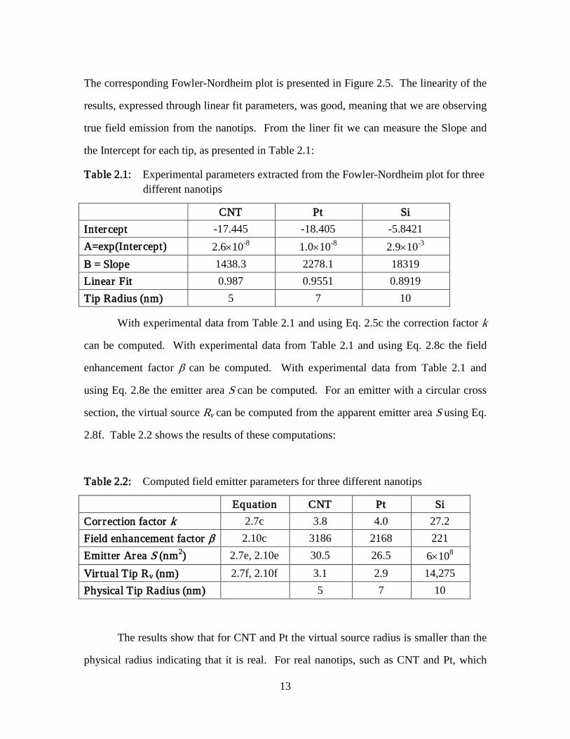
The corresponding Fowler-Nordheim plot is presented in Figure 2.5. The linearity of the
results, expressed through linear fit parameters, was good, meaning that we are observing
true field emission from the nanotips. From the liner fit we can measure the Slope and
the Intercept for each tip, as presented in Table 2.1:
Table 2.1: Experimental parameters extracted from the Fowler-Nordheim plot for three different nanotips
CNT Pt Si Intercept -17.445 -18.405 -5.8421 A=exp(Intercept) 2.6×10⁻⁸ 1.0×10⁻⁸ 2.9×10⁻³ B = Slope 1438.3 2278.1 18319 Linear Fit 0.987 0.9551 0.8919 Tip Radius (nm) 5 7 10
With experimental data from Table 2.1 and using Eq. 2.5c the correction factor k
can be computed. With experimental data from Table 2.1 and using Eq. 2.8c the field
enhancement factor β can be computed. With experimental data from Table 2.1 and
using Eq. 2.8e the emitter area S can be computed. For an emitter with a circular cross
section, the virtual source Rv can be computed from the apparent emitter area S using Eq.
2.8f. Table 2.2 shows the results of these computations:
Table 2.2: Computed field emitter parameters for three different nanotips
Equation CNT Pt Si Correction factor k 2.7c 3.8 4.0 27.2 Field enhancement factor β 2.10c 3186 2168 221 Emitter Area S (nm2) 2.7e, 2.10e 30.5 26.5 6×10⁸ Vir tual Tip Rv (nm) 2.7f, 2.10f 3.1 2.9 14,275 Physical Tip Radius (nm) 5 7 10
The results show that for CNT and Pt the virtual source radius is smaller than the
physical radius indicating that it is real. For real nanotips, such as CNT and Pt, which

14
resemble a spherical emitter on a cylindrical shank, the Fowler–Nordheim approximation
(Eq. 2.2) works well as shown by the results for the nanotips. For nanotips that deviate
from the model, such as the case with the Si tip that has large conical shank, the Fowler–
Nordheim approximation fails and the resulting virtual radius is computed to be much
larger than the physical radius which is not possible.
Chapters 4 and 5 of this work will use the above derived equations to demonstrate
and analyze field emission from a CNT emitter.

15
Chapter 3: Instrumentation and Components
In this Chapter we briefly describe the equipment and the components that were
used for the experiment to familiarize the reader with the experimental setup. The
instruments used for this work include a Scanning Electron Microscope, a
Nanomanipulator, a Gas Injection System, and a Field Emission Testing Vacuum
Chamber.
3.1 SCANNING ELECTRON MICROSCOPE (SEM)
The majority of the experiments presented in this work were conducted in a
Hitachi S-4000 non-environmental SEM equipped with a custom built gas
delivery/injection system and a custom built nanomanipulator, as shown in Figure 3.1.
This SEM was located at Xidex Corp. in Austin TX. This SEM was used for fabrication
of CNT emitters, evaluation of the CNT emitters, and for conducting experiments with
water assisted CNT editing. A second SEM used for the conducting CNT editing
experiments was a Hitachi S-4300SE/N variable pressure scanning electron microscope
(VPSEM), as shown in Figure 3.2, located at The University of Tennessee at Knoxville.
Also used for fabrication of CNT emitters and their evaluation was a dual-beam Focused
Ion Beam (FIB) and SEM tool, FEI Strata DB235 equipped with a Zyvex S100
nanomanipulator. This tool was located at The University of Texas at Austin, in
particular, at the Texas Materials Institute and Center for Nano- and Molecular Science.
Finally, some of the FIB ion-milling used in the fabrication of the lateral CNT emitters
was conducted with FIB tools located at SEMATECH in Austin TX (prior to their
relocation out of Austin).

16
SEMs are primarily used as imaging tools that allow viewing of nanometer sized
objects and materials, such as carbon nanotubes, Pt and W nanowires, gold nanoparticles,
and other nanostructures and nanomaterials. There is a new trend in nanotechnology to
use the SEM instrument as nanofabrication tool. For example with the help of
nanomanipulators, such as the NanoBot® nanomanipulator [3.1], we can fabricate CNT
based Scanning Probe Microscope (SPM) tips and CNT based emitters, which is the
subject of this work. With the help of gas injection systems, such as the Parallel Gas
Injection System (PGIS) [3.2], we can conduct electron beam induced etching and
deposition (EBIE/EBID) of materials inside the SEM, equivalent to a “nano-welding”
process. For example EBIE/EBID can be used to fabricate (attach and cut to length as an
example) the CNT emitters we report in this work.
The basic principle of a SEM is to eject a stream of electrons originating from an
emitter (cold, thermionic, or Schottky), accelerate these electrons towards a sample, and
focus them along the way, so that the electrons interact with the sample, and then detect
the secondary electrons (SE) and/or back-scattered electrons (BSE) resulting from the
electron-sample interaction. Secondary electrons result from inelastic scattering of the
Figure 3.1: Hitachi S-4000 SEM used for conducting the CNT editing experiments and for fabricating CNT emitters. Figure 3.2: Hitachi S-4300SE/N SEM and
customized gas injection system.

17
electrons from the sample atoms. This is the most common mode of SEM imaging.
Back scattered electrons result by elastic scattering of the electrons from the sample
atoms.
The SEM controls include its beam energy, beam current, and scan rates. We
used all three parameters to control the editing of CNTs as described in more detail in one
of the Chapters of this work. Beam energy can be varied by changing the accelerating
voltage. Typical SEM acceleration voltages are in the range of 1 to 30 keV, where lower
acceleration voltage produces lower beam energy. Lower beam energy does not charge
the sample but also produces lesser quality of image and vice versa for the higher energy.
The beam current is proportional to the flux of electrons. The incident beam current is
measured by a Faraday cup connected to a digital picoammeter. Typical beam currents
are in the range of pA to nA. The beam current can be modified by adjusting the
condenser lens settings, as well as by use of variable, current-limiting apertures. The
condenser lens concentrates (or demagnifies) the beam of electrons into a spot. The size
of the beam can therefore be adjusted. Typical analog condenser lens settings are from 1
to 10 where a higher number means smaller beam size and therefore lower beam current.
Typical computer controlled beam sizes are 1 to 5 where lower beam size means lower
beam current. Other types of control are: beam scanning rates, pixel dwell time, and
refresh rates. These parameters are unique to the SEM tool and the application. The
above parameters play an important role in the EBIE/EBID processes, including the CNT
editing that is subject to our work. For example we found that conditions for CNT
editing are 10 microsecond dwell time, 1 ms frame refresh rate, and 30 loops per second
in a line scan mode. The SEM operates in high vacuum mode with typical pressure
ranges from 5.0x10⁻⁴ Pa to 2.0x10⁻² Pa.

18
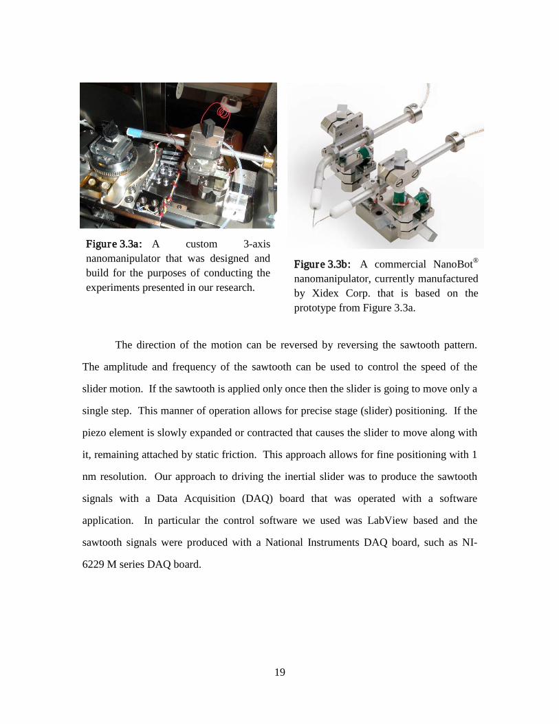
3.2 IN-SITU NANOMANIPULATOR
For the needs and requirements of our research work we have built a custom 3-
axis inertial slider type nanomanipulator that can operate inside the SEM chamber, as
shown in Figure 3.3. Each axis of the nanomanipulator consists of a stainless steel (SS)
base, a linear piezo element, a graphite bearing, and a SS slider that is clamped on the
bearing. In this assembly the piezo element is epoxied to the SS base using common high
vacuum epoxy, such as Varian Torr Seal. The graphite element is also epoxied to the
piezo element. The SS slider is clamped to the graphite bearing with two screws and a
beryllium copper spring inserted between the screw and the slider. The presence of the
spring allows us to control the clamping force between the slider and the bearing. The
nanomanipulator was able to move in 3 orthogonal axis, X, Y, and Z, with range of 15
mm by sliding along. At each point the piezo could operate as an ordinary piezo element
with ranges of ± 2.3 µm for voltages of ± 40 V. The resolution of this slider was
measured to be 1 nm and was only limited by the noise of the applied voltage.
The principle of operation of the inertial slider is as illustrated in Figure 3.4. As
shown in Figure 3.4a, the piezo element expands together with the graphite bearing that is
fixed to it. As shown in Figure 3.4b, the slider also moves forward along with the
graphite bearing since static friction is holding the slider clamped to the bearing. After
expanding with a desired amplitude the piezo element contracts quickly, exceeding the
static friction limit and allowing the bearing to return back to its original position while
the slider was left in the same place as the before the piezo contracted, as shown in Figure
3.4c. If this motion is repeated consecutively the slider will advance with each step while
the piezo and the bearing keep moving forward and backward. Clearly the key to the
motion is to expand and contract the piezo with a sawtooth pattern. During the slow
slope of the sawtooth the slider advances and during the fast slope of the sawtooth the
slider is left in place while the piezo and the bearing return back to zero, as shown in
Figure 3.4d.
19
The direction of the motion can be reversed by reversing the sawtooth pattern.
The amplitude and frequency of the sawtooth can be used to control the speed of the
slider motion. If the sawtooth is applied only once then the slider is going to move only a
single step. This manner of operation allows for precise stage (slider) positioning. If the
piezo element is slowly expanded or contracted that causes the slider to move along with
it, remaining attached by static friction. This approach allows for fine positioning with 1
nm resolution. Our approach to driving the inertial slider was to produce the sawtooth
signals with a Data Acquisition (DAQ) board that was operated with a software
application. In particular the control software we used was LabView based and the
sawtooth signals were produced with a National Instruments DAQ board, such as NI-
6229 M series DAQ board.
XYZ
Figure 3.3b: A commercial NanoBot® nanomanipulator, currently manufactured by Xidex Corp. that is based on the prototype from Figure 3.3a.
Figure 3.3a: A custom 3-axis nanomanipulator that was designed and build for the purposes of conducting the experiments presented in our research.

20
Figure 3.4: The principle of operation of an inertial linear stage
3.3 GAS INJECTION SYSTEM
Our research objectives required that we develop a custom gas injection system
(GIS) that would enable selective CNT etching at reduced background pressures suitable
for a non-environmental SEM instrument. Most conventional gas injection systems, like
the ones found in FIB tools, are based on a simple one-dimensional design which allows
the nozzle to move in only one direction, towards the center of the system, at the
intersection between the beam and the stage, to bring the nozzle close to the sample.
Using this conventional system the nozzle can be moved in XYZ from outside the
vacuum chamber within about 0.5 mm from the sample and with low precision of 100s of
microns. An example of a conventional gas injection system head with mechanical
wobble stick positioning control is shown in Figure 3.5. This is the system used by our
collaborators at the University of Tennessee. Our requirement was to have a GIS that can
enable closer approach of the nozzle and with better positioning precision.
Our custom gas injection system solution was to fix the gas injection nozzle to a
precision XYZ nanomanipulator to allow positioning of the gas delivery nozzle 10s of

21
Figure 3.6: Schematic of a gas injection system with a nozzle attached to a nanomanipulator for precise nozzle positioning. Option 2# has the gas reservoir inside the chamber.
microns away from the sample and with equally good precision. Figure 3.6 shows the
schematic of the concept. In one option of operation the gas reservoir is located outside
of the SEM chamber, and in Option#2 the gas reservoir is located inside the SEM
chamber.
XYZ Nanomanipulator
H2O
Gas Delivery Nozzle
Gas Injection Nozzle Option #2 Sample
Vacuum Feedthrough
SEM Sample Chamber
Sample Stage
H2O
Option #2 XYZ Nanomanipulator
Figure 3.5: Photographs of a) the gas injection flange, b) the gas delivery needle, and c) an SEM micrograph of the delivery needle in close proximity to the substrate.
a) b)
c)
22
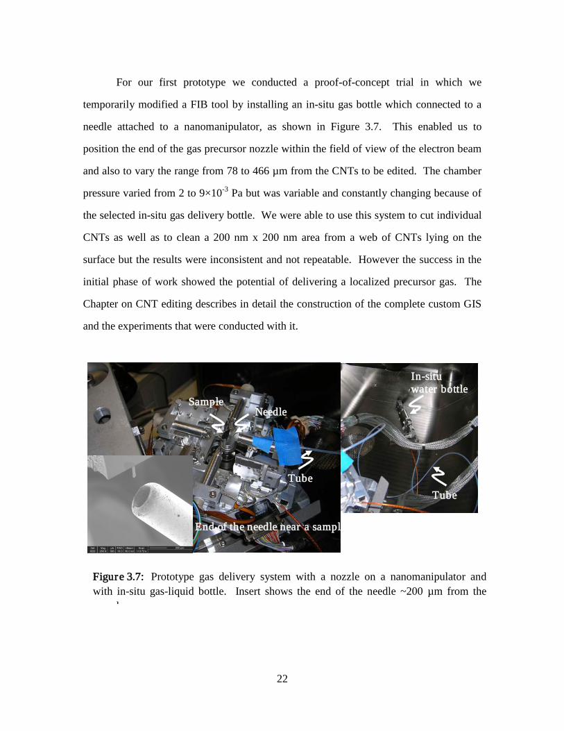
For our first prototype we conducted a proof-of-concept trial in which we
temporarily modified a FIB tool by installing an in-situ gas bottle which connected to a
needle attached to a nanomanipulator, as shown in Figure 3.7. This enabled us to
position the end of the gas precursor nozzle within the field of view of the electron beam
and also to vary the range from 78 to 466 µm from the CNTs to be edited. The chamber
pressure varied from 2 to 9×10⁻³ Pa but was variable and constantly changing because of
the selected in-situ gas delivery bottle. We were able to use this system to cut individual
CNTs as well as to clean a 200 nm x 200 nm area from a web of CNTs lying on the
surface but the results were inconsistent and not repeatable. However the success in the
initial phase of work showed the potential of delivering a localized precursor gas. The
Chapter on CNT editing describes in detail the construction of the complete custom GIS
and the experiments that were conducted with it.
Figure 3.7: Prototype gas delivery system with a nozzle on a nanomanipulator and with in-situ gas-liquid bottle. Insert shows the end of the needle ~200 µm from the
l
Needle
Tube
In-situ water bottle
Sample
End of the needle near a sample
Tube

23
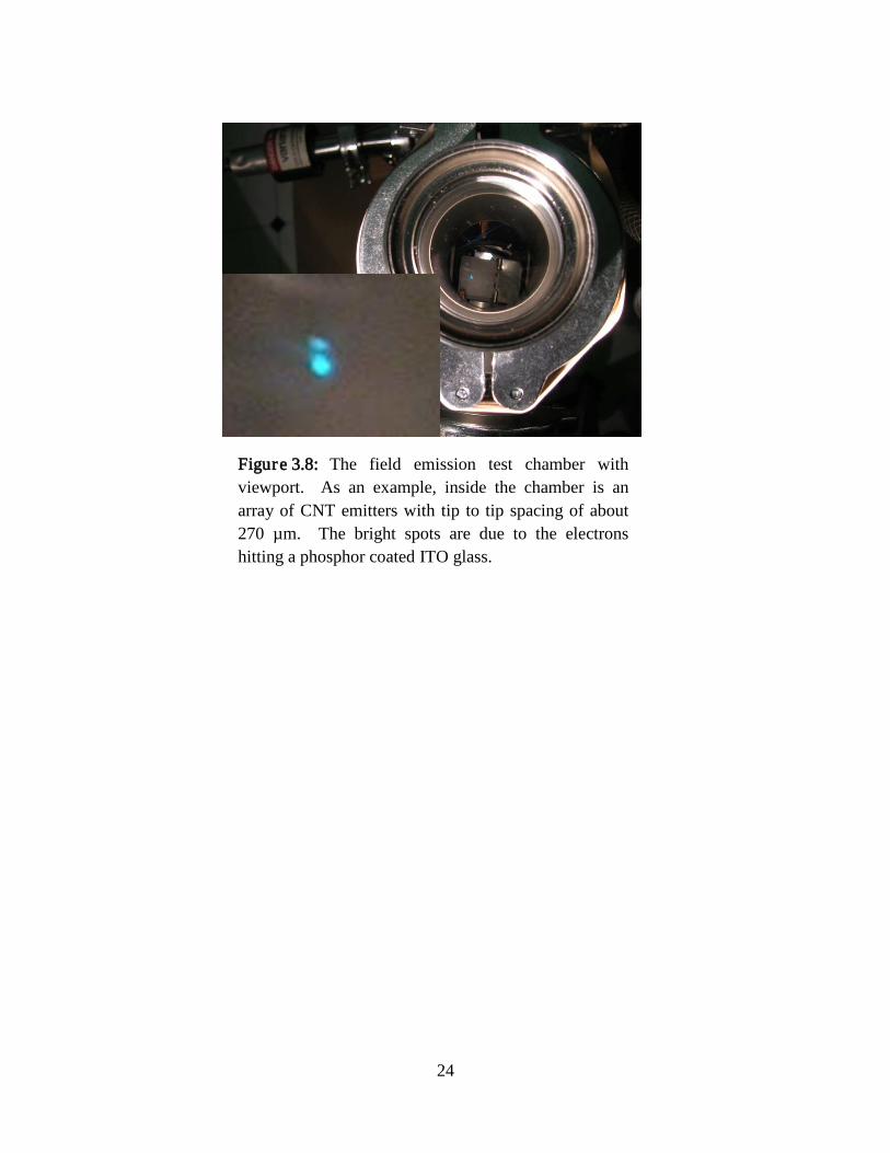
3.4 FIELD EMISSION EVALUATION HARDWARE
The performance of the CNT field emitters was investigated in a vacuum test
chamber specially built and dedicated for the field emission experiments. The
specialized vacuum test chamber consists of a pumping station and a cylindrical vacuum
chamber with a view-port, as shown in Figure 3.8. The pumping station consists of a
turbo-pump backed by a mechanical pump. The best vacuum level we have been able to
achieve with this station is 2×10⁻⁷ Torr. All the experiments were conducted at this level
of vacuum so as to demonstrate the utility of our CNT emitters in a high vacuum
environment. The vacuum is measured using a cold-cathode vacuum gauge that can
measure vacuum down to 1×10⁻⁸ Torr.
We used two types of sample holders, one for CNT emitters fabricated on a
silicon substrate and another for CNT emitters fabricated on a sharpened tungsten wire.
The former sample holder is made of two parallel glass plates coated with gold or
aluminum. The CNT emitter is fixed to the cathode plate with a carbon paste where the
anode plate is positioned above the emitter. The spacing is controlled with precision
machined Macor and quartz spacers. The later sample holder is made of a wire holder
with a set screw and a metal coated glass plate perpendicular to the wire. The anode-
cathode spacing is controlled by setting the gap under an optical microscope.
For diode type field emission measurements the electrical field was supplied with
a Keithley 237 current-voltage source that can provide up to 1100 V of bias. The I-V
tests ware run with an automated system consisting of LabView based software and
National Instruments hardware.
24
Figure 3.8: The field emission test chamber with viewport. As an example, inside the chamber is an array of CNT emitters with tip to tip spacing of about 270 µm. The bright spots are due to the electrons hitting a phosphor coated ITO glass.

25
Chapter 4: Carbon Nanotube Field Emitters as Sources for Scanning Electron Microscopes
4.1 INTRODUCTION
Many industries, including the semiconductor industry, as well as the emerging
nanotechnology industry, depend on scanning electron beam instruments, such as field
emission scanning electron microscopes (FE-SEMs), Schottky emitter based SEMs (for
example, critical dimension SEMs), and transmission electron microscopes (TEMs), to
develop new processes and products, control existing processes and stimulate new
innovations in materials science. Currently there is a need for significant improvement in
the spatial resolution, signal-to-noise ratio, and processing speed of these imaging tools.
This need can be met by improving either the electron optical column or the electron
source. Electron optical columns have improved significantly in the last 10-15 years
[4.1], however, the field emission source itself has basically not changed. The spatial
resolution of scanning electron beam instruments can be improved by a field emission
source with higher brightness, lower energy spread, and smaller emitter size [4.1, 4. 2,
4.3, 4.4]. An electron source with higher brightness can focus a larger amount of current
into a spot of a given size, resulting in shorter image acquisition time and faster
processing speed [4.2]. Smaller source size improves the source brightness by reducing
the spatial angular spread of the beam [4.4]. In addition, smaller source size lowers the
energy spread (distribution width) [4.4]. In scanning electron beam instruments the
source size of the emitter determines how much demagnification must be applied by the
electron optics of the column to achieve the desired resolution, where less
demagnification means better tool signal-to-noise ratio [4.1].
Furthermore, SEM / TEM users who utilize scanning electron microscopes for
high-precision measurements, such as those in the semiconductor industry, are also
concerned about emission stability. Precision is the gauge of how repeatable the
measurements are. For example, for semiconductor SEM users, a loss in precision means
26
that bad products are declared good or good products are declared bad, resulting in
diminished product yield. Fluctuations, noise, spikes, and drift of the emission current all
affect the short and long term stability of the electron beam and therefore the precision of
the microscope. The electron emission stability of the emitter depends on the quality of
the emitter, its erosion, its resilience to contamination and other environmental factors.
Finally, most SEM / TEM users care about long emitter lifetime and the
availability of commercial emitters. Long emitter lifetime reduces tool downtime and
lost productivity by reducing the frequency of changing the SEM / TEM filament and
reducing the frequency of tool calibration. Commercial SEM / TEM users are also
interested in the commercial availability of emitters as opposed to hearing and reading
about another “one-time” laboratory success that cannot be replicated or produced in
commercial quantities.
Therefore, the desired characteristics of an ideal emitter for scanning electron
beam instruments are high brightness, low energy spread, small emitter size, high
emission stability, long emitter lifetime, and commercial emitter availability. The
presented research will ultimately enable better field emitters for high-performance
electron beam instruments.
4.1.1 Conventional Cold Field Emitters
Conventional cold field emitters have advantages over Shottky based thermal
field emitters and thermionic field emitters because they do not require power
consumption for heating, they do not require evaporation of cathode material, they have
slightly better brightness, lower energy spreading, and reasonable emitter lifetime if the
emitter is maintained (flashed or briefly heated by applying large current pulse)
frequently [4.5]. Most common conventional cold field emitters are made of tungsten
and have a conical geometry with apex radius of 100 to 150 nm. Because of their

27
advantages cold field emitters are the preferred filaments for field emission SEMs /
TEMs where high imaging resolution is desired.
Disadvantages of conventional cold field emitters are their delicate environmental
stability and their susceptibility to contamination, leading to bad emission stability. In
particular, conventional cold field emitters, which are subject to being sputtered by
ionized residual gas molecules, are inclined to undergo chemical reactions with
molecules or ions of residual gases, and can change their work function and electron
affinity in the presence of ions or molecules on the emitter surface. The result of the
above interactions is emitter noise, field current reduction, and ultimately a destructive
shortening. As a result of their disadvantages the conventional cold field emitters require
high vacuum operation and need frequent flashing to eliminate any contaminants from
their surface.
One approach to circumvent the disadvantages of the cold field emitters and keep
the advantages of the Shottky based thermal field emitters is to use nanotip field emitters.
Qian et al. [4.6] and Purcell et al. [4.4] have demonstrated that nanotips offer higher
brightness and lower energy spread because of their small tip radius.
4.1.2 Nanotip Emitters
Nanotip emitters, by comparison to all conventional cold, thermally assisted, and
Schottky field emitters, offer a significant increase in brightness (10 to 100 times) and
large reduction (5 to 10 times) in source size. Use of nanotips is also expected to reduce
the Boersch effect as a result of a reduction in the total emitted current from the source
and the possibility of removing focal crossovers in the beam path.
We will shown that the best candidates for nano-sized high-aspect-ratio
cylindrical nanotips are carbon nanotube (CNT) nanotips. We next overview the
advantages of carbon nanotubes as promising field emitters through literature review.

28
The existing state-of-the art emitter sources are ZrO/W Schottky emitters with
high reduced brightness Br (2×10⁸ A m-2 sr-1 V-1), low energy spread (0.8 eV), a good
emission stability (less than 0.5%) and long lifetime (years) [4.2, 4.7]. Existing cold field
emitter sources are W emitters that have compatible (slightly better) reduced brightness
and lower energy spread (0.3 eV), but they have inferior emission stability (5%) [4.2] and
shorter lifetime (few months) than Schottky emitters.
4.1.3 Emitter Br ightness
The reduced brightness Br measures the amount of current that can be focused
into a spot of a certain size from a certain solid angle:
Br = I / (dΩ π rv2 V) = I’ / (π rv
2 V) (Eq. 4.1)
where I is the emission current (A), dΩ is the solid angle of the electron beam
spread (steradians), I’ is the angular current density (A sr-1), rv is the radius of the virtual
source (m), and V is the extraction voltage applied to the emitter. For nanotips with small
radius, a conservative estimate of the radius of the virtual source can be assumed to be
the radius of the nanotip, rv = RNT. Therefore, the brightness of an electron source is
better for smaller diameter nanotip and for higher emission currents at given extraction
voltage.
Several groups have directly or indirectly demonstrated that CNT nanotip emitters
have much better brightness then state-of-the art Schottky emitters or W cold field
emitter sources. de Jonge et al. [4.2, 4.8, 4.9, 4.10] have conducted comprehensive
experiments to directly determine the brightness of carbon nanotube field emitters. Using
a set of carbon nanotubes with lengths of about 1 µm and radius of less then 10 nm, de
Jonge has demonstrated an average value of the reduced angular current density of the
carbon nanotubes of 30 nA sr-1 V-1. The reduced-brightness for an individual carbon
nanotube emitter was between 1.3 and 2.5×10⁹ A m-2 sr-1 V-1, and order of magnitude
better than the values of state-of-the-art commercial emitters. Hata et al. [4.11] have also

29
demonstrated very high reduced-brightness for carbon nanotube emitters, 5.6×10⁹ A m-2
sr-1 V-1. These are the best brightness results from a nanotip emitter archived to date.
The nanotubes used in this experiment were 20 nm in diameter and were typically
mounted manually on a conductive wire for the purposes of their evaluation.
Guillorn et al. [4.12] indirectly show that good brightness can be achieved from a
nanotip. They demonstrated that less than 1% of the current emitted from carbon
nanofibers was collected by the gate, therefore indicating an excellent electron beam
collimation (small beam spreading). The size of the beam spread was not measured
directly. The advantage of this demonstration was that the nanotips were grown directly
on the substrate instead being manually mounted. The disadvantage of this
demonstration is that the nanotips were not cylindrical and were large. The nanotubes
used in this experiment were grown directly on a substrate using Plasma Enhanced CVD.
Their typical base diameter was 200 nm, with tip diameter of 15 nm, and height of 1 µm.
4.1.4 Emitter Stability and Lifetime
One of the great advantages of carbon nanotube emitters is their demonstrated
emission stability and long lifetime. Carbon nanotubes are far more resistant to
sputtering from ionized residual gas molecules than conventional field emission cathodes
composed of refractory metals [4.9, 4.13]. Carbon nanotube emitters also experience
negligible surface diffusion in the presence of large electric fields. Nanotube emitters
also are inert with respect to many residual gasses [4.9].
Dean et al. [4.14] have demonstrated excellent long-term (over 350 hours) field
emission stability from single wall carbon nanotube emitters with diameter of 0.7 to 1.2
nm. They tested the stability of the carbon nanotube emitter under influence of purified
H2O, Ar, H2, and O2. The carbon nanotube emitters only showed susceptibility to
damage by oxygen. Metal field emitters that were subjected to the same environmental
tests self-destructed after 10 hours. The conclusion of the finding was that carbon

30
nanotube emitters are more stable in poor vacuum then metal emitters. The advantage of
the carbon nanotube emitters was attributed to the emitter geometry, strong carbon
bonding, and lack of unwanted protrusion growths. Hsu et al. [4.15] have discovered that
treating the carbon nanotube emitters in a hydrogen environment produced an
enhancement of the carbon nanotube based field emission. Furthermore, carbon
nanotube emitters that have been degraded in oxygen can increase their emission current
340-fold after being exposed to hydrogen.
Bonard et al. [4.5] have investigated the current stability of individual carbon
nanotube emitters at a vacuum level of 10-7 mbar and found switching type current
fluctuations at lower currents. The emission was more stable at higher currents and at
deeper vacuum levels. An individual nanotube emitter was found to be stable for more
than 100 hours at 2 µA current. In another investigation Bonard et al. [4.3] have
demonstrated a field emission of more than 1400 hours at 0.5 µA at 4×10⁻⁷ mbar. Hsu et
al. [4.16] demonstrated that short term stability of carbon nanotube emitters was 5% from
the emission current but that there was general drift of the current. Fransen et al. [4.17]
have demonstrated a short-term stability of 1.2% in a continuous run that took 54 days.
The emission stability of any emitter may be regulated to some extent with a simple
feedback loop that keeps the emission current constant. de Jonge et al. [4.9] have
reported short-term current fluctuations of less than 0.5 % with the help of feedback loop.
4.1.5 Other Field Emitter Figures of Mer it
Utsumi [4.18] demonstrates that an ideal shape for a field emitter is a sphere but
that a “rounded whisker” (a cylindrical emitter where the radius of the hemispherical end
of the tip is half its diameter) geometry is the closest to the ideal sphere geometry.
Therefore, a very effective means of achieving large enhancement factors is to use high
aspect-ratio cylindrical tips as we propose here.
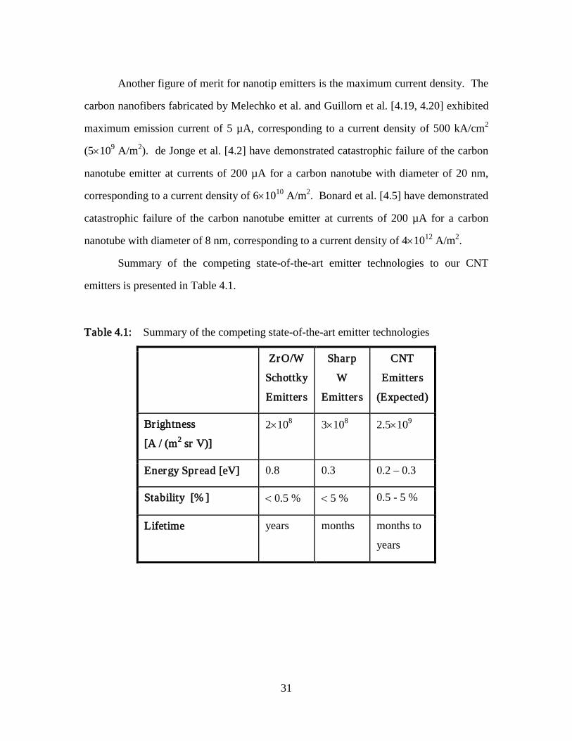
31
Another figure of merit for nanotip emitters is the maximum current density. The
carbon nanofibers fabricated by Melechko et al. and Guillorn et al. [4.19, 4.20] exhibited
maximum emission current of 5 µA, corresponding to a current density of 500 kA/cm2
(5×10⁹ A/m2). de Jonge et al. [4.2] have demonstrated catastrophic failure of the carbon
nanotube emitter at currents of 200 µA for a carbon nanotube with diameter of 20 nm,
corresponding to a current density of 6×10¹⁰ A/m2. Bonard et al. [4.5] have demonstrated
catastrophic failure of the carbon nanotube emitter at currents of 200 µA for a carbon
nanotube with diameter of 8 nm, corresponding to a current density of 4×10¹² A/m2.
Summary of the competing state-of-the-art emitter technologies to our CNT
emitters is presented in Table 4.1.
Table 4.1: Summary of the competing state-of-the-art emitter technologies
ZrO/W
Schottky
Emitters
Sharp
W
Emitters
CNT
Emitters
(Expected)
Br ightness
[A / (m2 sr V)]
2×10⁸ 3×10⁸ 2.5×10⁹
Energy Spread [eV] 0.8 0.3 0.2 – 0.3
Stability [% ] < 0.5 % < 5 % 0.5 - 5 %
Lifetime years months months to
years

32
4.2 FABRICATION
4.2.1 Fabr ication of Carbon Nanotube Field Emitter s
The CNT emitters used in this research were fabricated using two alternative
methods: manual mounting of carbon nanotubes and direct carbon nanotube growth. The
method of direct carbon nanotube growth was demonstrated only for a silicon substrate
(Figure 4.1a). The method of manual mounting was demonstrated for sharp silicon tip
substrate (Figure 4.1b) and sharpened tungsten substrate (Figure 4.1c). During this work
we made and tested more than 40 different CNT emitters, either grown or mounted, and
analyzed 27 CNT emitters.
4.2.2 Manual Mounting
Manual mounting of CNTs is the most common approach for fabricating CNT
tips and emitters. The following issues arise when one attempts to fabricate CNT
emitters or tips.
a) Published information shows that researchers’ main supply of nanotubes for
mounting are nanotubes fabricated using arc-discharge or CVD growth and either
Figure 4.1a: CNT emitter grown directly on Si tip
a) b) c)
Figure 4.1c: CNT emitter manually mounted on a sharpened W tip
Figure 4.1b: CNT emitter manually mounted on a Si tip

33
dispensed in a solvent solution or collected on a carbon tape. Either approach requires
additional processing or handling of the CNTs that can contaminate the CNTs.
Our approach to the supply of nanotubes was to grow straight, clean, high quality
carbon nanotubes directly on the edge of a silicon substrate using thermal CVD process.
Afterwards, the CNT can be directly picked up from the Si substrate without any
intermediate preparation process. The tips fabricated in this research used this method.
b) Typically, manual CNT mounting procedures take place inside an SEM
chamber and with the help of a nanomanipulator. It is common procedure to first contact
the CNT to a sharp W tip, and then attach the CNT to the W tip by applying glue to the
CNT-W junction or by depositing carbon from hydrocarbon contamination to the CNT-
W junction. Alternatively one can also deposit metal from a metal precursor source
instead carbon. Afterwards the CNT is pulled out from the bundle by retracting the tip.
With this approach there is no control over the length of the CNTs and after one failed
attempt the W probe (with the failed CNT) have to be replaced.
Our method of attaching the CNT to the tip (Si or W) was to first contact the CNT
with the tip. The presence of Van der Waals force will snap any small diameter CNT to
the tip where it would stay in contact unless the tip is pulled away from the CNT. In
practice any CNT with diameter of 40 nm or less would readily snap to a W or Si tip.
Applying a current pulse, producing current induced Joule heating, would cut the CNT
away from the substrate and will attach it to the W tip. Although the length of the CNT is
not precisely controlled, there is some control over the length of the CNT. The added
benefit of this approach is that for each mounted CNT we know the current limits that
would cause its cutting and destruction. This information was used to estimate the
maximum current that can be applied to each CNT emitter. More detailed description of
the manual CNT mounting procedure is presented in Appendix A (also reference [4.21])
and recorded on a YouTube video [4.22]. For a more controlled fabrication of a CNT

34
emitter tip we have used a water vapor induced CNT etching/cutting approach that is
described in detail in Chapter 6 of this work.
c) Most CNT tips are fabricated with lack of control over the alignment of the
CNT with respect to the substrate. However, it is desired to have an aligned CNT emitter
with respect to the mounting substrate. The alignment assures that the CNT apex is the
closest point to the anode and the source of the electron emission.
There is very limited research and published information that describes a method
of aligning a CNT emitter after it has mounted on a W wire. Park et al. [4.23] has
described use of Focused Ion Beam (FIB) to align a carbon nanotube on a silicon
substrate and use it as a scanning probe tip.
Our method of aligning the CNT emitter was to use a FIB beam for an alignment,
after the CNT has been mounted on the W wire. The results of this approach are shown
in Figure 4.2.
A CNT that was irradiated with a low dose of Ga+ ions (for example by operating
the ion beam with low 10 pA beam current) tended to align itself in the direction of the
ion beam. The conductivity of the CNT after the Ga+ irradiation had increased. The
mechanism of the increase is not well understood but it could be the removal of defects in
the CNT lattice, the removal of contaminants from the CNTs, or a deposition of Ga atoms
Figure 4.2: Illustration of focused ion beam assisted carbon nanotube alignment. a) CNT before alignment, b) CNT after alignment
a) before b) after

35
on the CNT. In general, the FIB aligned CNT emitters performed better then non-aligned
CNT emitters.
d) Another variation in the fabrication of CNT emitters on sharp W tips was to
change the sharpness of the W tip. We produced electrochemically sharpened W tips
with average end radius of 25 - 50 nm, as shown in Figure 4.3a. Well known methods
and apparatuses were utilized for tip etching/sharpening. We also tested the use of
focused ion beam (FIB) sharpening of W wires which were previously electrochemically
sharpened, to produce W tips with 5 - 10 nm end radius that proved to be the best base for
the CNT emitters, as shown in Figure 4.3b. The results show that CNT emitters made on
sharper W tips performed better then the CNT emitters made on blunter W tips. This
indicates that the end radius of the W tips plays a greater role in defining the electrostatic
screening effect (the shield effect) than we had anticipated.
4.2.3 Direct CNT Growth
The method of direct carbon nanotube growth was demonstrated only for a silicon
SPM substrate. The procedure was as follows. Standard silicon based SPM tips, such as
a) b)
Figure 4.3: Examples of a) electrochemically sharpened W tip, and b) focused ion beam sharpened W tip

36
Budget Tap 300 [4.24], were first cleaned with clean and dry compressed nitrogen to
remove any large contaminants. Subsequently, the tips were carefully dipped into
solutions containing catalytic material. The SPM tips were then placed in a CVD oven
and the CNTs were grown using thermal CVD process. Typical CVD recipes were
conducted with a flow rate of Ar/H2 1000-2000 sccm to 1 sccm of ethylene at growth
temperature of 750°C for 10 minutes. The flow of the carrier gas and the precursor gas
into the CVD oven were slowed down until a single CNT would statistically grow on 1
out of 5 CNT tips. Most tips would have multiple CNTs or single not well positioned or
aligned CNT tip. A CNT tip successfully fabricated by this method of directly growing a
single nanotube at the apex of a sharp silicon tip is shown in Figure 4.4. CNT emitters
grown on silicon SPM substrates cannot easily be mounted on standard scanning electron
beam instruments but are great test samples used to study the mechanism of CNT
emission.
4.2.4 Competing Nanotube Tip Fabr ication Processes
In contrast to our thermal CVD process is the Plasma Enhanced CVD process for
growing aligned carbon nanofibers directly on a substrate. This method of carbon
Figure 4.4: Gallery of carbon nanotube tips grown directly on silicon SPM tips. Average CNT diameter is ~ 10 nm.

37
nanotube fabrication is for example practiced by the Meyyappan group from NASA
Ames Research Center and the Molecular-Scale Engineering and Nanoscale Technology
Research Group at Oak Ridge National Laboratory (ORNL). The ORNL group was also
very involved in fabricating “vertically aligned carbon nanofibers” (VACNFs) as field
emitters for the flat panel display applications. The disadvantages of the Plasma
Enhanced CVD process is that small diameter (less than 50 nm) multiwalled CNT are
hard to produce. In addition, the carbon nanotubes grown with the plasma enhanced
CVD method are relatively contaminated with graphite and other oxide and nitride
contaminants. Typical carbon nanofibers fabricated by Melechko et al. and Guillorn et
al. [4.19, 4.20] are quite large and conical, with base diameter of 200 nm, tip diameter of
25 nm, and height of 2 µm. Therefore, we believe that VACNFs are not suitable as field
emitters for scanning electron beam instruments.
Other research groups have fabricated carbon nanotube based emitters directly on
the substrate but they have not been able to achieve the quality and the rate of production
that we have. For example, Minh et al. [4.25] demonstrated a fabrication process for
growing carbon nanotube emitters with diameter from 4 to 200 nm on top of sharp Si tips
and have demonstrated a field emission from an individual nanotube. Zhang et al. [4.26]
have demonstrated a fabrication process for depositing carbon nanotube emitters on W
tips via dielectrophoresis. The disadvantage of this fabrication method is that most of the
time the nanotip is comprised of bundles of nanotubes staggered on top of each other
until one protrudes further than the others. We do not know if there are unwanted effects
of this staggered tip on field emission. Nevertheless, Zhang et al. [4.26] have
demonstrated field emission from an individual carbon nanotube emitter, deposited on the
W tip via dielectrophoresis, with 50 nm diameter exhibiting maximum emission current
of 5 µA and a modest current density of 2.5×10⁵ A/m2. The beam divergence of this field
emitter was unusually large, 50°.

38
4.2.5 Emitter Fabr ication Improvements
The baseline CNT emitter was fabricated on W or Si tip and was tested. The
electrical tests of the CNT emitters as they were fabricated showed that the electrical
connection between the CNT and the substrate varied and was not consistent. Therefore,
we improved the CNT emitter fabrication process by depositing carbon and platinum on
the CNT-substrate junction with a goal to improve the electrical connection. The C and
the Pt were deposited using electron beam induced metal deposition techniques with the
help of a Gas Injection System. More detailed study of the electrical properties of a CNT
tip is presented in Appendix B. The results of the improved CNT emitter fabrication on
the performance of the CNT emitter are discussed in the results section below.
4.2.6 Field Emission Testing Hardware
The field emission test rig that used in this research is shown in Figure 4.5. The
electrical field for emission measurements was supplied with Keithley 237 current-
voltage source that can provide up to 1100 V of bias. The data collection was done with
an automated system consisting of LabView based software and National Instruments
hardware that are already available on one computer.
We used two types of sample holders, one for CNT emitters fabricated on a
silicon substrate and another for CNT emitters fabricated on a sharpened tungsten wire.
The wire sample holder is shown in Figure 4.6. The phosphor plate is not shown in this
Figure.

39
4.3 EXPERIMENTAL RESULTS
4.3.1 Measurement and Evaluation of CNT Emitters
The field emission figures-of-merit measured during this research were: high
reduced brightness, high reduced angular current density, small virtual source size, small
emitter size, low noise, stability, and long lifetime.
The most important figure-of-merit about the performance of the CNT emitter is
the reduced brightness. The reduced brightness Br measures the amount of current that
can be focused into a spot of a certain size from a certain solid angle and was computed
according to:
Br = I / (dΩ π Rv2 V) = Ir’ / (π Rv
2) (copy of Eq. 1)
where I is the emission current (A), dΩ is the solid angle of the electron beam
spread (steradians), Ir’ is the reduced angular current density (A sr-1 V-1), Rv is the radius
of the virtual source (m), and V is the applied extraction voltage to the emitter (V).
Figure 4.6: Holder for testing CNT emitters on W wire
Figure 4.5: Field emission testing rig.

40
The independent parameters measured were: the I-V curves, the emission current
I, the applied extraction voltage V, the radius of the field emission pattern, and the radius
of the CNT emitter RCNT. We also had to measure the tip-to-anode distance d, and we had
to assume the work-function for a carbon nanotube φ. From these known parameters we
computed: the solid angle of the electron beam spread dΩ, the angular current density I’,
the reduced angular current density Ir’, the field enhancement factor β, the virtual source
size Rv, and the reduced brightness Br.
The spread of the electron beam dΩ was measured indirectly by measuring the
radius of the emission pattern on a phosphor screen located distance d away from the
emission source. The image of the field emission pattern was digitally recorded with a
camera and its radius was determined with intensity analysis (see Figure 4.7). To assure
that the spread of the electron beam dΩ was measured from a stable emitter we measured
the emission current for the duration of recording the image of the field emission pattern.
Figure 4.7: a) The image of the field emission pattern digitally recorded with a camera, where its radius was determined with intensity analysis (in this example R was 87 µm for a gap of 408 µm), b) normalized intensity plot, c) normalized contour plot.
b) a) c)
-600-300
0300
600
-600-300
0300
6000
0.2
0.4
0.6
0.8
1
X Microns
NORMALIZED PHOSPHOR SPOT INTENSITY
Y Microns0
0.1
0.2
0.3
0.4
0.5
0.6
0.7
0.8
0.9
1
-600 -300 0 300 600-600
-300
0
300
600
X Microns
Y M
icro
ns
NORMALIZED PHOSPHOR SPOT INTENSITY CONTOURS
0.1
0.2
0.3
0.4
0.5
0.6
0.7
0.8
0.9

41
Figures 4.8 and 4.9 show the average emission current and the current noise for
Emitter #1 and Emitter #2 respectively. The images of the field emission pattern for
Emitter #1 were measured at four different current levels, as shown in Figure 4.8. The
images of the field emission pattern for Emitter #2 were measured at three different tip-
to-anode distances, as shown in Figure 4.9. From the radius of the bright spot and the tip-
to-anode distance d we computed the solid angle of the electron beam spread dΩ
(steradians). The typical tip-to-anode distance was in the range of 50 µm up to 800 µm
which resulted in typical solid-angle beam spread in the range of 0.067 steradians to
0.482 steradians (full cone angle of 16.8° to 45.2°). Due to the small tip-to-anode
distance the field emission pattern was not magnified enough to observe the emission
from the individual atoms at the end of the nanotube but it was enough to measure the
spread of the electron beam.
The ratio between the emission current I and the beam spread solid-angle dΩ
gives us the angular current density I’, and the angular current density I normalized with
respect to the extraction voltage V gives as the reduced angular current density Ir’.
Figure 4.8: Field emission as recorded during brightness measurements for Emitter #1. Legend: (average current/extraction voltage/current noise/gap)

42
Typical angular current density ranges measured were 2-22 (µA sr-1) and the reduced
angular current density 11-81 (nA sr-1 V-1).
The radius of the virtual source Rv was derived from the measured I-V curves, as
described in Chapter 2. First, it is assumed that the I-V curves from the nanotube field
emission follow the Fowler-Nordheim approximation for field emission. A linearity of
the data in a Fowler-Nordheim plot, expressed through linear fit parameters, indicates an
evidence of a field emission. Therefore, from the slope and the ordinate intercept line of
the best linear fit one can determine the parameters of the field emission curve (see
Figure 4.10). Fitting the I-V curve into a Fowler-Nordheim plot we can extract the
enhancement factors β, the apparent emitting area S, and the virtual source Rv. The
results of testing two CNT emitters at different currents (Emitter #1) and at different tip-
to-anode distances (Emitter #2) showed virtual source radius ~2.2 nm, a realistic result
for CNTs with known radius of 5 nm.
Figure 4.9: Field emission (average of 2 or 3 runs) as recorded during brightness measurements for Emitter #2. Legend: (average current/extraction voltage/current noise/gap)

43
From the computed reduced angular current density Ir’ and the radius of the
virtual source Rv we computed the reduced brightness Br of the CNT emitters. The best
reduced brightness Br achieved was 6.1×10⁹ and 2.1×10⁹ A m-2 sr-1 V-1 for Emitter #1 and
Emitter #2 respectively. Tables 4.2 and 4.3 show a summary of the best experimentally
determined figures-of-merit related to the reduced brightness. Table 4.2 shows the
summary of the figures-of-merit for Emitter #1 which was tested at varying currents
levels and Table 4.3 shows the summary for Emitter #2 which was tested at varying tip-
to-anode distances. Computation of the virtual source radius Rv for the Emitter #1 was
obtained by averaging of 16 measured I-V curves and from the computed linear fit for the
high current regime in the Fowler-Nordheim plot, as shown in Figure 4.10. Computation
of the virtual source radius Rv for the Emitter #2 was obtained by averaging of 26 to 40
measured I-V curves and from the computed linear fit for the high current regime in the
Fowler-Nordheim plot, as shown in Figure 4.11. The reduced brightness for Emitter #2,
Gap#2 had unrealistically high value due to the unusually small virtual source radius (0.2
nm) as compared to the other experimental data. Therefore we do not report this data
point as real and verified.
a)
Figure 4.10: Data for Emitter #1 tests, a) average of 16 measured I-V curves and the computed fit for the high current regime, b) corresponding Fowler-Nordheim plot and the computed linear fit for the high current regime.
b)
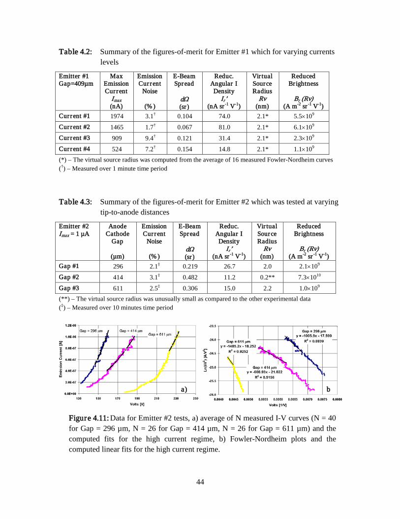
44
Table 4.2: Summary of the figures-of-merit for Emitter #1 which for varying currents levels
Emitter #1 Gap=409µm
Max Emission Cur rent
Imax (nA)
Emission Cur rent
Noise
(% )
E-Beam Spread
dΩ (sr )
Reduc. Angular I Density
Ir’ (nA sr -1 V-1)
Vir tual Source Radius
Rv (nm)
Reduced Br ightness
Br (Rv)
(A m-2 sr -1 V-1) Cur rent #1 1974 3.1† 0.104 74.0 2.1* 5.5×109 Cur rent #2 1465 1.7† 0.067 81.0 2.1* 6.1×109 Cur rent #3 909 9.4† 0.121 31.4 2.1* 2.3×109 Cur rent #4 524 7.2† 0.154 14.8 2.1* 1.1×109 (*) – The virtual source radius was computed from the average of 16 measured Fowler-Nordheim curves (†) – Measured over 1 minute time period
Table 4.3: Summary of the figures-of-merit for Emitter #2 which was tested at varying tip-to-anode distances
Emitter #2 Imax = 1 µA
Anode Cathode
Gap
(µm)
Emission Cur rent
Noise
(% )
E-Beam Spread
dΩ (sr )
Reduc. Angular I Density
Ir’ (nA sr -1 V-1)
Vir tual Source Radius
Rv (nm)
Reduced Br ightness
Br (Rv)
(A m-2 sr -1 V-1) Gap #1 296 2.1‡ 0.219 26.7 2.0 2.1×10⁹ Gap #2 414 3.1‡ 0.482 11.2 0.2** 7.3×10¹⁰ Gap #3 611 2.5‡ 0.306 15.0 2.2 1.0×10⁹ (**) – The virtual source radius was unusually small as compared to the other experimental data (‡) – Measured over 10 minutes time period
Figure 4.11: Data for Emitter #2 tests, a) average of N measured I-V curves (N = 40 for Gap = 296 µm, N = 26 for Gap = 414 µm, N = 26 for Gap = 611 µm) and the computed fits for the high current regime, b) Fowler-Nordheim plots and the computed linear fits for the high current regime.
a) b

45
The brightness results were comparable to the best brightness results from a
nanotip emitter achieved to date. Our results were about 10% better than the best
brightness results from a nanotip emitter archived to date as reported by Jonge et al.
[4.28, 4.29, 4.30] and Hata et. al [4.31]. A conservative estimate of the reduced
brightness can be computed assuming that the radius of the virtual source Rv was equal to
the radius RCNT of the carbon nanotube emitter. With this assumption (Rv = RCNT), the
conservative estimate of the reduced brightness was 1.0×10⁹ A m-2 sr-1 V-1 for our best
CNT emitter. This conservative estimate establishes that the lower bound of the reduced
brightness measured with our CNT field emitters.
Measuring the energy spread of the nanotip emitter was not conducted due to the
high cost and the complexity of the experimental setup. Instead we use an average values
found in the literature. For carbon nanotube emitters the reported energy spread was 0.2
to 0.3 eV.
The other field emission figures-of-merit measured were CNT emitter noise and
lifetime. We observed that the I-V curves of the CNT emitters had very high slope that
made them unstable for small changes in the voltage. To provide stability to the system
we decided to test each CNT emitter with a ballast resistor Rb added in series to the
emitter. The consequence of adding the ballast resistor is that the I-V curves become
flattened and the therefore more stable. We tested different values of added Rb between
100 kΩ and 100 MΩ and decided to bias each test with 100 MΩ ballast resistor. The
consequence of adding the ballast resistor was that before any I-V analysis we had to
correct the I-V curve and remove the effects of the added serial resistance. The values for
I were unchanged and the values for the extraction voltage were corrected as:
Vcorrected = Vmeasured – Imeasured × R100MΩ
We verified the validity of the above correction by generating an I-V curve for a
CNT emitter array with a Rb of 500 kΩ and correcting the I-V curve to show that when it

46
corrected it matches an I-V curve generated without use of ballast resistor, as shown in
Figure 4.12.
The noise and lifetime test were always recorded for all CNT emitters. During
this research we tested more than 40 different CNT emitters and analyzed 27 CNT
emitters. From the 27 CNT emitters we considered 21 CNT emitters that could reach
stable emission. The duration of the tests was from 1 min to 600 min with average test
lasting about 235 min. The average noise level of the entire set of 21 CNT emitters was
6.0%. The best CNT emitter that was grown on a Si base had a noise of 50 nA for an
average current of 2878 nA, or 1.7% for 10 hour time test (Figure 4.13a). The best CNT
emitter that was mounted on W base had a noise of 47 nA for an average current of 956
nA, or 4.9% for 10 hour time test (Figure 4.13b). If we compare the noise level in
percentages, then the best CNT emitter on W had a noise 2.3% (66 nA for an average
current of 2831 nA) for 300 minute time test. All the tests were conducted in open loop.
Figure 4.12: Correction of an I-V curve with a 500 kΩ ballast resistor in series with the CNT emitter array to match an I-V curve with 0 kΩ ballast resistor. The CNT emitter array in this example had Imax = 420 µA.

47
In future work we plan to build a feedback controller to better stabilize the emission
current, especially emission drift.
Since we only had one field emission test rig, the duration of the tests was limited
to no more than 600 minutes (10 hours) so that we could evaluate a larger number of tips
and be able to compare their performance.
4.3.2 Testing of the CNT emitter in an SEM instrument
In a first of its kind, we also
demonstrated that the CNT emitters can
be used with commercial SEM
instruments. The first task in evaluating
the CNT emitters in a commercial SEM
was to build an SEM filament holders on
which a CNT emitter can easily be
mounted and un-mounted for evaluation
purposes. Previously, we obtained a
Figure 4.13: 10 hours time test for two CNT emitters: a) CNT grown on Si, I = 3 µm, Inoise = 50 nA or 1.7% b) CNT mounted on W, I = 1 µm, Inoise = 47 nA or 4.9%
Figure 4.14: SEM filament holder for CNT emitter, a) holder used in initial
trials, b) CAD model of the new holder design.
a) b)

48
couple of Hitachi type SEM filaments from ScanService Corp. that we used for holder
evaluation and re-design. A practical solution was to remove the existing W filament and
replace it with a hollow stainless steel tube that was used to insert a 10 to 20 mm long W
wire with a CNT emitter on it (Figure 4.14a). Unfortunately, the SS tube was spot
welded in place. The spot-welding provided poor control over the tube alignment. We
have subsequently designed a SEM filament holder that slips on the existing Hitachi type
SEM filament base (Figure 4.14b) but did not get chance to build it. Due to its bulkiness,
this design does not allow for controllable heating of the emitter, but can be used for
CNT emitter evaluation in a commercial Hitachi SEM tool. In future, we plan to improve
the holder design to allow for controllable heating of the CNT emitter that may be needed
to remove contaminants before the emitter is evaluated.
Our team and ScanService Corp. evaluated two CNT emitters and briefly operated
the SEM to image a sample. It has to be noted that the CNT emitters were severely
misaligned at nearly 45° and were not optimal. The SEM testing required that we use our
special SEM filament holder and required that we modify a commercial scanning electron
microscope (SEM) tool to allow CNT emitter testing. The main SEM modification was
the change of the amplifier gains to the extraction voltages of the tool. Due to the lower
turn-on voltages CNT emitters need an order of magnitude less extraction voltage for
their operation. A special LabView data acquisition system was connected to the SEM to
control it emission and to collect data. In future we plan to work on modifying a
dedicated SEM in the manner we did on the pre-trials and improve the control of the
SEM experiments.
Figure 4.15 shows the I-V curves of the CNT emitters as operated in the SEM and
Figure 4.16 shows the time and stability test during brief SEM operation. The initial
SEM tests of the CNT emitters showed that CNT emission in a commercial tool is
feasible and exposed the problems we need to solve to improve the SEM evaluation. For
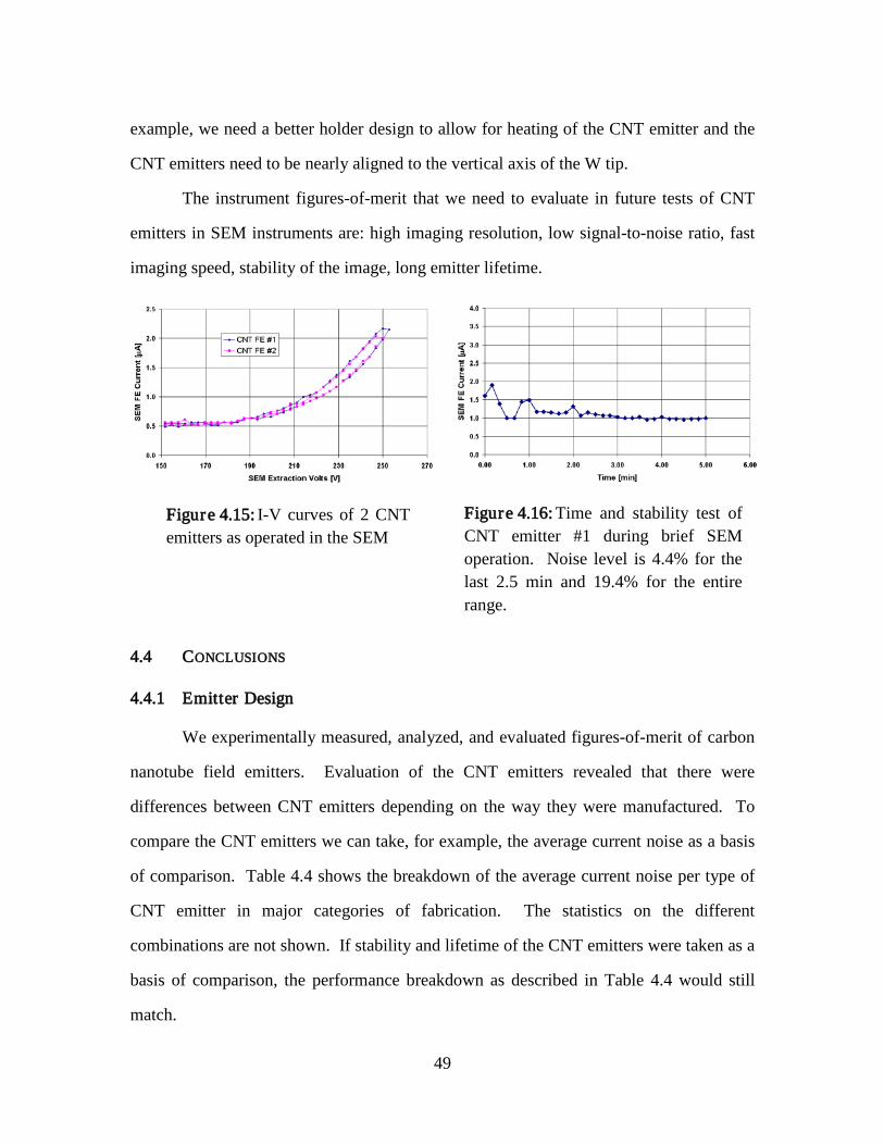
49
example, we need a better holder design to allow for heating of the CNT emitter and the
CNT emitters need to be nearly aligned to the vertical axis of the W tip.
The instrument figures-of-merit that we need to evaluate in future tests of CNT
emitters in SEM instruments are: high imaging resolution, low signal-to-noise ratio, fast
imaging speed, stability of the image, long emitter lifetime.
4.4 CONCLUSIONS
4.4.1 Emitter Design
We experimentally measured, analyzed, and evaluated figures-of-merit of carbon
nanotube field emitters. Evaluation of the CNT emitters revealed that there were
differences between CNT emitters depending on the way they were manufactured. To
compare the CNT emitters we can take, for example, the average current noise as a basis
of comparison. Table 4.4 shows the breakdown of the average current noise per type of
CNT emitter in major categories of fabrication. The statistics on the different
combinations are not shown. If stability and lifetime of the CNT emitters were taken as a
basis of comparison, the performance breakdown as described in Table 4.4 would still
match.
Figure 4.15: I-V curves of 2 CNT emitters as operated in the SEM
Figure 4.16: Time and stability test of CNT emitter #1 during brief SEM operation. Noise level is 4.4% for the last 2.5 min and 19.4% for the entire range.

50
4.4.2 CNT Emitter Fabr ication
By testing numerous CNT emitters that we fabricated during this research, we
have shown that in average they have suitable high brightness, small size, high stability,
and long lifetime. The results and findings are summarized as follows:
i) On average, CNT emitters on Si substrates performed better then CNT emitters
on W substrates. These were the main two types of CNT emitters we evaluated. Our
explanation is that the contact resistance between the CNT and the W is greater than the
contact resistance between the CNT and the Si, and as a result the CNTs on Si were more
stable.
ii) Since we did not have CNTs grown on W we compared CNT emitters grown
on Si vs. CNT emitters mounted on Si. On average, CNT emitters grown directly on
silicon substrates performed better then CNT emitters mounted on Si substrates. Our
explanation is that the contact resistance between the CNT and the bare Si is greater than
the contact resistance between the CNT and the Si covered with catalyst and CNTs laying
Table 4.4: Evaluation of set of 21 CNT emitters

51
on the surface. Confirming this finding is the observation that the mounted CNT emitters
were unstable with jumpy emission current. Nevertheless, CNTs on Si, wherever grown
or mounted, performed better then CNTs on W.
iii) To improve the contact resistance between the CNT emitter and the W base
we started welding the base of the CNT to the W with carbon and Pt depositions. This
approach significantly improved the performance of the W based CNT emitters. There
was however a difference between using only carbon welds and only Pt welds. CNTs
with Pt welds performed better. Our explanation is that oxidation of the W base
contributed to poorer electrical contact between the CNT and the W, whereas the Pt
deposition protected the W better from oxidation. We concluded that a tungsten based
CNT emitter design has to have a process step to protect the contact from oxidation.
iv) The alignment of the CNT emitter did not play a role in the noise and lifetime
of the emitter as long as the nanotube was within 45° from the base, which we consider to
be a large misalignment. We do not know how misalignment affects the beam spread and
the brightness.
v) After we solved the problems with the contact resistance between the CNT and
the substrate and addressed the CNT failures at the base of the emitter we started
observing CNT emitter failures along their length. In particular, most CNT emitter
failures were caused by gradual or sudden shortenings of the nanotube, as shown in
Figure 4.17, until it was all removed. The failure was a function of the maximum
emission current to which the emitter was exposed. For CNT emitters on W most failures
occurred at currents of more than 2 µA and for CNT emitters on Si most failures occurred
at currents of more than 4 µA. Our explanation is that defects and contamination along
the length of the CNTs started to play role in the CNT emitter failure. It is also possible
that the open ends of the CNTs were the contributing failure mechanism.
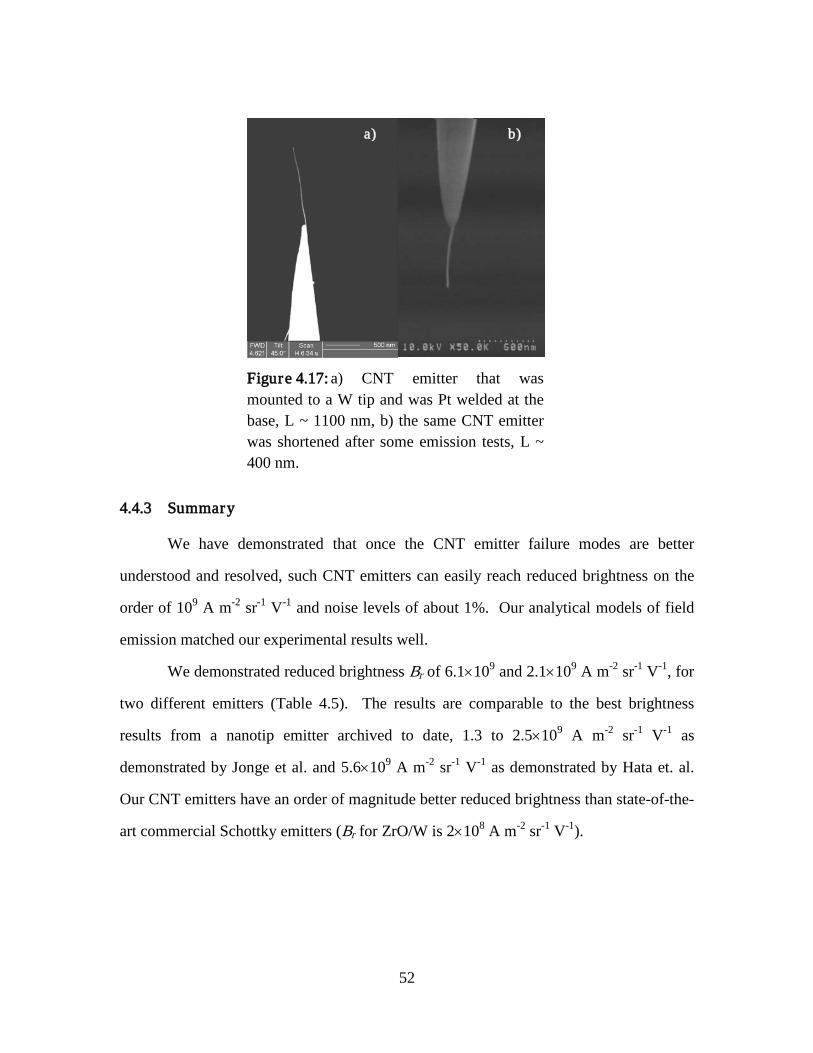
52
4.4.3 Summary
We have demonstrated that once the CNT emitter failure modes are better
understood and resolved, such CNT emitters can easily reach reduced brightness on the
order of 109 A m-2 sr-1 V-1 and noise levels of about 1%. Our analytical models of field
emission matched our experimental results well.
We demonstrated reduced brightness Br of 6.1×10⁹ and 2.1×10⁹ A m-2 sr-1 V-1, for
two different emitters (Table 4.5). The results are comparable to the best brightness
results from a nanotip emitter archived to date, 1.3 to 2.5×10⁹ A m-2 sr-1 V-1 as
demonstrated by Jonge et al. and 5.6×10⁹ A m-2 sr-1 V-1 as demonstrated by Hata et. al.
Our CNT emitters have an order of magnitude better reduced brightness than state-of-the-
art commercial Schottky emitters (Br for ZrO/W is 2×10⁸ A m-2 sr-1 V-1).
Figure 4.17: a) CNT emitter that was mounted to a W tip and was Pt welded at the base, L ~ 1100 nm, b) the same CNT emitter was shortened after some emission tests, L ~ 400 nm.
a) b)

53
Table 4.5: Summary of the best two CNT emitters
Best results
Max Emission Cur rent
Imax (nA)
Emission Cur rent
Noise
(% )
E-Beam Spread
dΩ (sr )
Reduc. Angul. I Density
Ir’ (nA sr -1 V-1)
Vir tual Source Radius
Rv (nm)
Reduced Br ightness
Br (Rv)
(A m-2 sr -1 V-1) Emitter #1 1465 1.7† 0.067 81.0 2.1 6.1×10⁹ Emitter #2 986 2.1‡ 0.219 26.7 2.0 2.1×10⁹ (†) – Measured over 1 minute time period (‡) – Measured over 10 minutes time period
We also demonstrated CNT emitters with excellent emission stability and low
noise of less than 5 % and a tip life of 10 hours without any degradation at all. The best
CNT emitter that was grown on Si base had a noise of 50 nA for an average current of
2878 nA, or 1.7% for 10 hour time test. The best CNT emitter that was mounted on W
base had a noise of 47 nA for an average current of 956 nA, or 4.9% for 10 hour time
test. If we compare the noise level in percentages, then the best CNT emitter on W had a
noise 2.3% (66 nA for an average current of 2831 nA) for 300 minutes time test. All the
tests were conducted in open loop, without any feedback. With a feedback loop we may
be able to reach a noise level of less than 1 %.
Using the data from the 10 hour test we predict that
emissions lasting 6 months are possible.
We had an opportunity to evaluate our CNT
emitters in a modified commercial scanning electron
microscope (SEM) tool and briefly operated the
SEM to image a sample, as shown in Figure 4.18.
Therefore, we demonstrated a proof-of-concept of
operating an SEM instrument with a CNT emitter.
Figure 4.18: A camera photo of an SEM screen, demonstrating a proof-of-concept of operating an SEM instrument with a CNT emitter.

54
4.5 FUTURE RESEARCH
4.5.1 Emitter Energy Spread Measurement
One important parameter in improving the resolution of scanning electron beam
instruments is to use an electron source that has low energy spread. Energy spreads lead
to chromatic aberration of the electron optical system, reducing the resolution of the
instrument. An energy spread of an electron source is defined as the full width at half
maximum of the energy spectrum and it is determined by the temperature T and the
tunneling parameter d. The tunneling parameter on the other hand is determined by the
electrical field from the emitter E and the emitter work function φ.
It has been demonstrated that CNT nanotip emitters have much lower energy
spread than state-of-the art Schottky emitters and either lower than or the same as W cold
field emitters. Bonard et al. [4.3] and de Jonge et al. [4.9] have measured and
demonstrated that carbon nanotube emitters have very low energy spread in the ranges of
0.2 to 0.3 eV. Fransen et al. [4.17] have measured energy spreads from carbon nanotubes
down to 0.11 eV.
Because the emission current depends on the work-function as φ3/2 / V, where V is
the applied electric field, lowering of the work-function can have dramatic effects. Morin
et al. [4.31] have shown that Cs adsorption on a sharp W tip decreased the work-function
from 4.5 eV to 1.6 eV while at the same time the energy spread decreased by a factor of
3.
In future research we plan to experimentally measure the CNT emitter energy
spread. At this time, we plan to also explore new ways to lower the energy spread of the
nanotips by lowering the work-function of our tip [4.31, 4.32]. One way to achieve this
goal is to coat the nanotips with a low work-function material such as Cs, ZrC, HfC, or
the like. The width of the energy spread should also scale down with the work function.

55
4.5.2 Vir tual Source Measurements
In the future we also plan to improve the resolution of the measured radius of the
virtual source. One approach will be to use a Field Ion Microscope (FIM) to get a clean
field emission pattern magnified enough to observe the emission from the individual
atoms. Optionally, one can build a point projection microscope to measure the virtual
source of the CNT emitters. The point projection microscope can be build in accordance
with the descriptions of de Jonge [4.8]. In this technique the emitter is positioned with a
help of a XYZ nanomanipulator above a sharp edge inside a FIM. The presence of the
sharp edge on front of the ion flow produces diffraction pattern representative of the
emission source, thus enabling the measurement of the virtual source.

56
Chapter 5: Lateral Carbon Nanotube Field Emitters
5.1 INTRODUCTION
The need of modern vacuum electronic devices requiring high current densities
and high total current, and fast and simple operation without the use of an external energy
source (such as a heater, or intense light source), has motivated the pursuit of a new field
emission current sources. This requirement eliminates the use of hot thermionic cathodes
which have slow response and require an external heating source.
There has been significant effort to build microwave vacuum electron devices
using cold cathodes to replace the existing hot thermionic cathodes. The most common
approach has been the use of Spindt type field emission array (FEA) cathodes [5.21].
However this approach has failed to produce practical, useful devices to date.
Field emission arrays based on cold cathode carbon nanotubes have caught the
attention of the research community as an attractive solution for achieving practical
vacuum electron devices, such as microwave vacuum amplifiers and X-ray sources.
Milne et al. [5.1] provides a comprehensive chart of the competing vertically aligned
carbon nanotube technologies.
Today's field emitters can achieve more than 10 µA of current from a single
emitter tip. In addition, such field emitters can be packaged into arrays with anywhere
from 1 million to 100 million tips/cm2. Thus far, however, emission non-uniformity has
prevented such field emission arrays from achieving large total currents (> 1 A). Field
emission currents of 1 A and greater and current densities of 10 A/cm2 and greater can
enable a new generation of microwave devices suitable for radar and communications,
high power microwave devices for directed energy applications, medical x-ray sources,
ionization/neutralization sources for spacecraft propulsion, and flat-panel field emission
displays.

57
The goal of this research was to demonstrate a novel emitter device in order to
reduce the variation in the current from emitter to emitter, thereby allowing high current
density operation with high total current.
CNTs have been identified as ideal field emission sources because of their
nanometer-scale dimensions, high aspect ratio, chemical inertness, excellent electrical
properties, and mechanical strength. CNTs are far more resistant to sputtering from
ionized residual gas molecules than conventional field emission cathodes composed of
refractory metals, and they are inert with respect to many residual gasses. Previous
research has also shown that CNTs in any form factor (individual, bundles, film, forest)
have field emission properties that are better then their sharp metal emitter counterparts.
Prior research has shown that individual, vertically aligned CNTs, as opposed to
CNT bundles and films, exhibit low turn-on voltage (1 V/µm), high emission current (0.2
mA), and corresponding high emission current density (4×10⁸ A/cm2). However, as a
result of electrostatic screening effects, the high emission currents from an individual
emitter may not translate directly to an equivalent emission current from a large sample
containing many such emitters. This is true whether the emitter is CNT based or metal
based. This is also true for any array elements comprising individual, bundle, or film
form-factors. Previous research has shown that an optimal CNT based field emission
array is one where the emitter-to-emitter distance is balanced with respect to its length.
Therefore, for achieving large emission currents with a field emission array, it is
desirable to fabricate an array consisting of strategically distributed nanotube elements,
with elimination/reduction of the screening effect in mind.
Previous research has shown that, as a result of any length non-uniformities
among vertically aligned CNTs in the array, it is expected that the emission from the field
emitter array may also be non-uniform, leading to hot-spots and possible overheating and
self destruction.
58
5.1.1 Related Work
There has been an unprecedented amount of work in the area of carbon nanotubes
over the past decade. Among all the amazing properties of CNTs, their field emission
characteristics have been extensively studied and analyzed. We will briefly overview
some the research work in the field of CNT based high emission current sources and
describe our advantages over these approaches.
Bonard et al. [5.2] have reported the highest current density to date from an
individual manually mounted CNT, 4×10⁸ A/cm2. Chen et al. [5.3] have reported the
highest current density from an array to date. They claim a stable field emission current
density of more than 6 A/cm2 for an electric field of 7.7 V/µm and a total current of > 1.2
mA. Their result was achieved with a bundle of CNTs packed in a 70 µm diameter and
patterned as 4 dots spaced 2 mm apart. The apparent record for the highest current
density from an array appears to have been set by Bower et al. [5.4]. Bower et al. have
reported a current density of 16 A/cm2 from an array of 9 patterns of a CNT forest, each
with dimensions of 10×10 µm. However, they normalize the current density by the
emission area of the nanotubes and not the total area of the array. Their total current was
150 µA or 16 µA per CNT bundle. Manohara et al. [5.5] have reported field emission
current density of more than 6 A/cm2 for an electric field of 20 V/µm and 1.8 A/cm2 for
an electric field of 4 V/µm from a 100 µm diameter area separated in patterns of CNT
bundles with 2 µm bundle and 5 µm spacing. The CNTs were grown using thermal CVD
and with sample patterning. The authors have investigated the optimal emitter bundle
size and spacing for maximum field emission. Their approach is to break up the CNT
bundle into smaller bundle patterns and then optimize their spacing. Their findings about
emitter (bundle) size and spacing do not match the one conducted by Nilsson et al. [5.6]
and Suh et al. [7], indicating that the array spacing design highly depends on the type of
CNTs (bundles, film, forest) and the packing density. Nilsson et al. [5.6] have shown
through simulations and experiments that the optimum nanotube packing density occurs

59
when the inter nanotube spacing is twice the nanotube height. Suh et al. [5.7] have
shown that the optimal nanotube spacing is equal to the nanotube height. Nilsson et al.
have shown that the uniformity of the field emission from patterned films (forests) of
CNTs was the best when the nanotube packing was with medium density. Their poor
high-density CNT film performance was explained by the electrostatic screening effects,
and the poor performance of their low density CNT film was explained by the non-
aligned morphology of the individual CNTs. A simulation by Nilsson et al. showed that
for aligned CNT emitters with 1 µm height the ideal density is 2.5×10⁷ emitters/cm2.
Milne et al. [5.1] has reported high current densities of about 1 A/cm2 and 1.5 GHz signal
modulation capability from a CNT cold cathode. Their optimized CNT array was
constructed from individual CNT emitters, grown via PE CVD, with CNT heights of 5
µm, CNT diameter of 50 nm, emitter spacing of 10 µm, and a total emission area of
500×500 µm. The advantage of their array is that the emitter is a single CNT with only
4% deviation in diameter and 6% deviation in height across all CNTs in the array. The
disadvantage is the large size of the CNT and probably their more amorphous then
crystalline morphology, typical for plasma assisted CNT growth.
There are a pair of research works related to field emission from the CNT
sidewall. Chai et al. [5.8] have demonstrated a field emission from the sidewall of a bent
individual multiwall CNT loop mounted atop a metal wire. They operated the emitters in
a very low current range, 1-100 nA and briefly demonstrated 5 µA, and mainly
investigated the turn-on voltages. Their findings were that CNT loops have smaller turn-
on voltages and higher enhancement factors β than CNT tips. Konishi et al. [5.9] have
also demonstrated a field emission from the sidewall of a bent individual multiwall
carbon nanotube mounted atop a W wire. Their finding is contradictory to the one of
Chai et al. Konishi et al. who have reported that CNT loops have larger turn-on voltages
than strait CNTs. Konishi et al. also reports sidewall emission that is 2.8 times larger
than that of the emission from the tip of a CNT but they do not report the emission

60
current. Jung et al. [5.10] have reported field emission from horizontal CNT film grown
in cracks of a substrate and reported a current density of 77 mA/cm2 but their CNT
quality is poor and the CNTs are too dense. Chen et al. [5.11] have reported that highly
packed CNT lying horizontally on the surface have smaller turn-on voltage then
nanotubes vertically oriented on the substrate.
In this work we present a solution for the non-uniformity of emission problem
with a novel lateral CNT emitter design that incorporates horizontally aligned CNTs
suspended on silicon posts wherein the electron emission occurs from the sidewall of the
carbon nanotube as opposed to the end of the nanotube as is commonly done. The main
advantage of emission from horizontal nanotubes is that the entire carbon nanotube
network lies in the same plane, without any protrusions, therefore eliminating non-
uniformities among the nanotube emitters. Our approach to designing an optimal CNT
array is to fabricate the CNTs suspended on an array of conical or cylindrical silicon
posts, where the spacing of the posts, the lengths of the CNTs, and the nanotube-to-
nanotube emitter spacing are all controlled. The preferred lateral CNT emitter element
design incorporates single horizontally aligned carbon nanotube, which is nanometers in
diameter, suspended on two microns-tall silicon posts spaced microns apart. An array of
lateral CNT emitter elements would incorporate many such elements spaced microns
apart, as illustrated in Figure 5.1. Although horizontally suspended CNTs have been
manufactured in the past and have been used for many applications (mainly sensors,
resonators, and prototype transistors) we have not encountered other research which has
investigated their use as field emitters. We report here an observation of field emission
from a lateral CNT emitter element.

61
5.2 EXPERIMENTAL RESULTS
5.2.1 CNT Lateral Emitter Substrate Fabr ication
Fabrication of the substrate for the lateral field emitter is the first task that needs
to be resolved before fabricating the emitter device. The preferred substrate for our
design is a pair of high aspect ratio posts that serve as a template from which the
suspended CNT emitters are fabricated. Besides acting as a fabrication template, the
presence of high aspect ratio posts will help elevate the CNT emitters from the surface,
effectively reducing the electrostatic screening effect with respect to the surface. We
anticipate that posts with heights between 2 to 10 µm are sufficient to significantly
reduce the screening effect.
Figure 5.1: Schematic drawing of lateral CNT emitter design and ranges of the key dimensions.
2-5 µm
Anode
I 1-5 µm
Si
CNT
Anode
I
2-10 µm
10-100 µm
Si
CNT CNT

62
The simplest substrate for the simplest lateral-emission element with a single
suspended carbon nanotube is high aspect ratio Pt or W pillars that can be fabricated
using e-beam induced deposition (EBID), as shown in Figure 5.2a, or W or Si knife-
edges that can be ion-milled from a sharp W or Si tip, as shown in Figure 5.2b. For this
work we used dual-beam FIB tool capable of Pt and W deposition and ion-milling. The
ion-milling is less precise and produces knife-edge pillars as opposed to the more precise
deposited pillars which can have diameters between 35-100 nm, lengths between 1-5 µm,
and spacing between 1-10 µm. This technique is also suitable for fabricating an emitter
array with Pt/W/Si pillars with different heights and separation, but practically limited to
an array of no more than 2×2 or 3×3 pillars. Emitter arrays requiring more than 9 pillars
need to be done using silicon micro-fabrication technology.
5.2.2 Manual CNT Lateral Emitter Fabr ication
The simplest lateral-emission element with a single suspended carbon nanotube
was fabricated manually as shown in Figure 5.3. A dual-beam FIB/SEM tool equipped
with nanomanipulator was used to manually suspend an individual carbon nanotube over
two posts. In this procedure the free end of a cantilevered CNT (from a sample rich with
Figure 5.2: (a) Pt pillars on the apex of a sharp Si tip, fabricated using e-beam induced deposition technique. (b) Ion-milled W to produce knife-edge pillars for growing or mounting CNT emitters.
a) b)
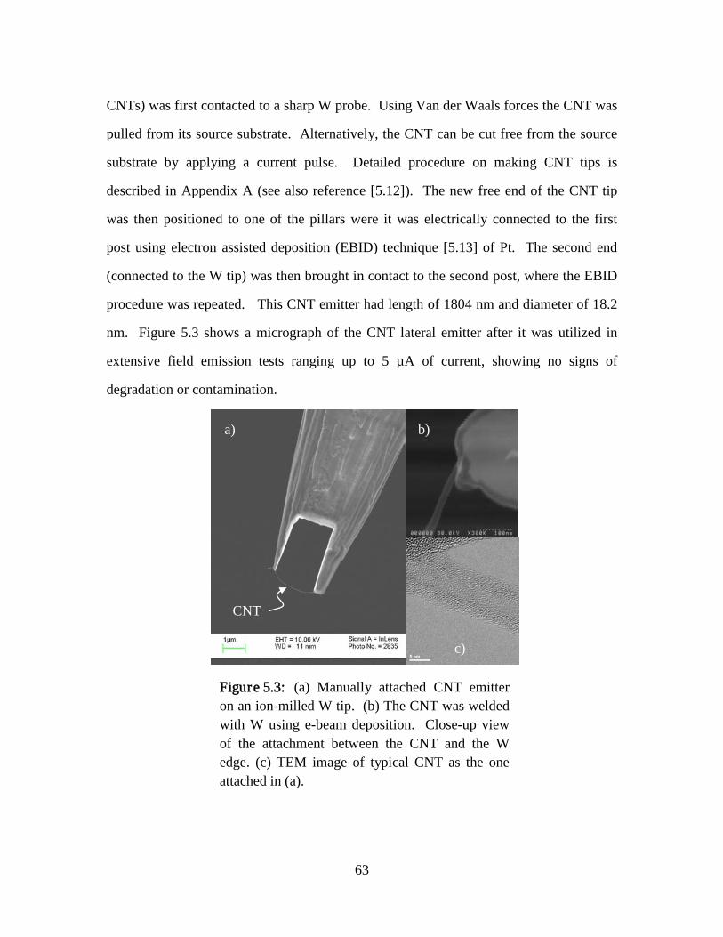
63
CNTs) was first contacted to a sharp W probe. Using Van der Waals forces the CNT was
pulled from its source substrate. Alternatively, the CNT can be cut free from the source
substrate by applying a current pulse. Detailed procedure on making CNT tips is
described in Appendix A (see also reference [5.12]). The new free end of the CNT tip
was then positioned to one of the pillars were it was electrically connected to the first
post using electron assisted deposition (EBID) technique [5.13] of Pt. The second end
(connected to the W tip) was then brought in contact to the second post, where the EBID
procedure was repeated. This CNT emitter had length of 1804 nm and diameter of 18.2
nm. Figure 5.3 shows a micrograph of the CNT lateral emitter after it was utilized in
extensive field emission tests ranging up to 5 µA of current, showing no signs of
degradation or contamination.
Figure 5.3: (a) Manually attached CNT emitter on an ion-milled W tip. (b) The CNT was welded with W using e-beam deposition. Close-up view of the attachment between the CNT and the W edge. (c) TEM image of typical CNT as the one attached in (a).
a)
CNT
b)
c)
64
5.2.3 CNT Lateral Emitter Fabr ication with Direct CNT Growth
Alternatively we fabricated a lateral CNT emitter by directly growing the CNT on
the ion-milled Si posts. In this procedure the Si posts were ion-milled on top of a
standard scanning probe microscopy (SPM) tip. The SPM tip with ion-milled posts was
first cleaned with clean and dry compressed nitrogen to remove any large contaminants.
Subsequently, the tip was carefully dipped into solutions containing catalytic material.
The SPM tips were then placed in a CVD oven in such manner that the flow of the carrier
and precursor gas during the CVD process is perpendicular to the posts. The CNT
emitter was grown using thermal CVD process. Typical CVD recipes were conducted
with a flow rate of Ar/H2 1000-2000 sccm to 1 sccm of ethylene at growth temperature of
750°C for 1 min. The CVD process produces horizontally suspended CNTs from sharp
knife-edge Si posts, as shown in Figure 5.4. Due to the larger width of the knife-edge Si
posts there were more than one CNT spanning the gap (Figure 5.4a and 5.4b) but we have
shown that a single CNT can also be grown (Figure 5.4c). We believe that the yield of
making single CNT emitters will improve once we reduce the size of the posts. The
process for growing horizontal CNTs is repeatable and shows promises that will work on
large array of posts.

65
5.2.4 Evaluation of the CNT Lateral Emitter
We report a successful emission from a lateral CNT emitter element having a
single suspended CNT. We report a field emission from the manually made lateral field
emitter from Figure 5.3, the grown lateral field emitters from Figure 5.4 and several other
grown emitters. There was no significant difference in performance based on the way the
CNT emitter was fabricated.
The tests were conducted in a custom vacuum chamber, equipped with a view-
port suitable for taking images of the field emission. The average vacuum level for the
tests was ~ 1×10⁻⁶ Torr. We had two types of sample holders, one for CNT emitters
fabricated on a SPM tip substrate and another for CNT emitters fabricated on a sharpened
tungsten wire. The former sample holder is made of two parallel glass plates coated with
gold or aluminum. The CNT emitter is fixed to the cathode plate with a carbon paste
where the anode plate is positioned above the emitter. The spacing is controlled with
precision machined Macor and quartz spacers. The latter sample holder is made of a wire
holder with a set screw and a metal coated glass plate perpendicular to the wire. The
Figure 5.4: Examples of three lateral-emission CNT emitters. The Si substrate was ion-milled to fabricate a gap. The CNTs were grown directly using CVD process. Few extra CNTs in the gap were removed for sample (a) and (b). Sample (c) grew only a single CNT.
b) CNT CNT c)
CNT
a)

66
anode-cathode spacing is controlled by setting the gap under an optical microscope. For
diode type field emission measurements the electrical field is supplied with Keithley 237
current-voltage source that can provide up to 1100 V of bias. The I-V tests were run with
an automated system consisting of LabView based software and National Instruments
hardware.
The independent parameters we can measure are: the emission current I, the
applied extraction voltage V, the size of the field emission pattern, and the radius of the
CNT emitter RCNT. We also had to measure the tip-to-anode distance d, and we had to
assume the work-function for a carbon nanotube φ. From these parameters we computed:
the solid angle of the electron beam spread dΩ, the angular current density I’, the reduced
angular current density Ir’, the field enhancement factor β, the virtual source area Sv, and
the reduced brightness Br. The spread of the emission pattern was measured by placing a
transparent glass coated with ITO and phosphorus as the anode. The result of the
measurement was a bright spot or spots on the screen as a result of the electron
bombardments. From the radius of the bright spot and the source to screen distance we
can compute the solid angle of the electron beam spread dΩ (steradians). The ratio
between the emission current I (A) and the beam spread solid-angle dΩ (sr) will give us
the required angular current density I’ (A sr-1).
The virtual source of an electron emitter is the area S = π rv2 from which the
electrons appear to originate from when they are traced back along their trajectories. For
nanotips with small radius, a conservative estimate of the radius of the virtual source rv
(m) can be assumed to be the radius of the nanotip, rv = RNT. For our carbon-nanotube
emitters this approximation holds well because the typical diameter of our carbon-
nanotube nanotips is 10 nm and less.
Table 5.1 lists the summary of the most relevant figures-of-merit for field emitters
and compares the performances between the vertical field emitter to the manually
fabricated lateral field emitter. The results show that field emission from a lateral CNT
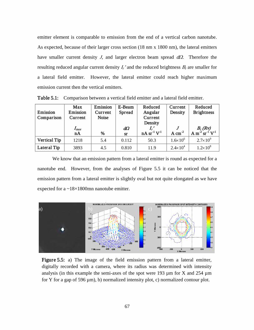
67
emitter element is comparable to emission from the end of a vertical carbon nanotube.
As expected, because of their larger cross section (18 nm x 1800 nm), the lateral emitters
have smaller current density J, and larger electron beam spread dΩ. Therefore the
resulting reduced angular current density Ir’ and the reduced brightness Br are smaller for
a lateral field emitter. However, the lateral emitter could reach higher maximum
emission current then the vertical emitters.
Table 5.1: Comparison between a vertical field emitter and a lateral field emitter.
Emission Comparison
Max Emission Cur rent
Imax nA
Emission Cur rent
Noise
%
E-Beam Spread
dΩ sr
Reduced Angular Cur rent Density
Ir’ nA sr -1 V-1
Cur rent Density
J A cm-2
Reduced Brightness
Br (Rv) A m-2 sr -1 V-1
Ver tical Tip 1218 5.4 0.112 50.3 1.6×10⁶ 2.7×10⁹ Lateral Tip 3893 4.5 0.810 11.9 2.4×10⁴ 1.2×10⁸
We know that an emission pattern from a lateral emitter is round as expected for a
nanotube end. However, from the analyses of Figure 5.5 it can be noticed that the
emission pattern from a lateral emitter is slightly oval but not quite elongated as we have
expected for a ~18×1800mn nanotube emitter.
Figure 5.5: a) The image of the field emission pattern from a lateral emitter, digitally recorded with a camera, where its radius was determined with intensity analysis (in this example the semi-axes of the spot were 193 µm for X and 254 µm for Y for a gap of 596 µm), b) normalized intensity plot, c) normalized contour plot.
a) b) c)

68
We also measured the noise and stability of the field emission over time of 30 min
to up to 720 min. We tested the grown-CNT lateral field emitter for 12 hour at 8.6 µA,
as shown in Figure 5.6b, without any CNT failure. The maximum emission current we
could demonstrate was actually limited by the maximum voltage possible with the power
supply and the tip-anode gap we have selected. The emission noises were compatible to
the vertically aligned CNT emitters, as shown in Figure 5.6a, but the lateral CNT emitter
could be used at almost double the maximum current then the vertical CNT emitter.
5.3 LATERAL ARRAYS
Since we have demonstrated the operation of a single element of a lateral CNT
emitter, we next plan to demonstrate the feasibility of a lateral-emission CNT device
having multiple carbon nanotube elements arranged in an array.
To demonstrate the feasibility of a large array of lateral CNT emitters with
density of 106-107 nanotubes/cm2 where most nanotubes are suspended horizontally on
tall Si posts we need to fabricate an array of silicon posts with 3 µm post spacing and
active area of 2×2 mm where the post density would be 107 tips/cm2. Assuming that each
horizontally aligned CNT emitters produces emission current of 5 µA when screening
effects of the neighboring CNT element are accounted for, then the array current density
could be computed as follows. For a sample with tip density of 107 emitters/cm2 (3 µm
Figure 5.6: Long time stability and noise test for (a) Si and W based vertical CNT emitters and (b) Si based lateral field emitter.
a) b)
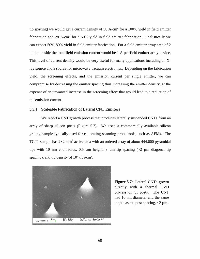
69
tip spacing) we would get a current density of 56 A/cm2 for a 100% yield in field emitter
fabrication and 28 A/cm2 for a 50% yield in field emitter fabrication. Realistically we
can expect 50%-80% yield in field emitter fabrication. For a field emitter array area of 2
mm on a side the total field emission current would be 1 A per field emitter array device.
This level of current density would be very useful for many applications including an X-
ray source and a source for microwave vacuum electronics. Depending on the fabrication
yield, the screening effects, and the emission current per single emitter, we can
compromise by decreasing the emitter spacing thus increasing the emitter density, at the
expense of an unwanted increase in the screening effect that would lead to a reduction of
the emission current.
5.3.1 Scaleable Fabr ication of Lateral CNT Emitters
We report a CNT growth process that produces laterally suspended CNTs from an
array of sharp silicon posts (Figure 5.7). We used a commercially available silicon
grating sample typically used for calibrating scanning probe tools, such as AFMs. The
TGT1 sample has 2×2 mm2 active area with an ordered array of about 444,000 pyramidal
tips with 10 nm end radius, 0.5 µm height, 3 µm tip spacing (~2 µm diagonal tip
spacing), and tip density of 107 tips/cm2.
Figure 5.7: Lateral CNTs grown directly with a thermal CVD process on Si posts. The CNT had 10 nm diameter and the same length as the post spacing, ~2 µm.

70
The substrate, and the Si tips, were coated with catalyst by dipping the sample
into solutions containing catalytic material. The array of Si tips was then placed in a
CVD oven in such manner that the flow of the carrier and precursor gas during the CVD
process is perpendicular to the posts. The CNT emitter was grown using thermal CVD
process. At the time of this experiment we did not have a thermal evaporator available.
The preferred methods of catalyst deposition includes thermal evaporation and sputtering,
which can deposit thin metal films with angstroms precision over the size of a wafer.
The lateral CNT growth process was standard thermal CVD process that is known
to produce high quality carbon nanotubes. A mixture of ethylene (C2H4) and hydrogen
(H2) are used as the precursor gasses and argon (Ar) or nitrogen (N2) is used as the carrier
gas. Typical CVD temperature is 750ºC for 10 minutes. During the growth process the
CNTs nucleate from the catalytic particle on the Si tip and span across the substrate to
reach another catalytic particle in its vicinity. In our experience one key parameter to
adjust in this process is the total gas flow rate as function of the post spacing.
We have fabricated some number of CNTs that were spanning from one tip to
another. Some fraction of carbon nanotubes grew from tip to tip. We believe that our
results would have been even better if the tips had been sharper and if the catalyst were to
be deposited only on the apexes. SEM images revealed that the array tips were
significantly blunter (100-200 nm diameter) then the expected 10 nm radius. However,
these results show a process that is feasible to produce an array with laterally aligned and
suspended CNTs. We also show small arrays (2×2 and 3×3) of suspended CNT, as
shown in Figure 5.8. The instances where we have multiple CNTs suspended between
two posts is small. From the initial array of 87 posts we estimate that 70% of the Si posts
have a CNT starting or terminating there, about 40% of the CNTs bridge from post to
post (anywhere on the post), even smaller percentage of CNTs are suspended from the
tips of both posts. The growth of CNTs that do not contact any post is minimal.
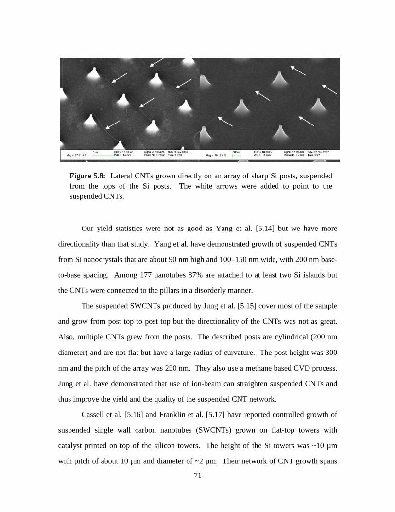
71
Our yield statistics were not as good as Yang et al. [5.14] but we have more
directionality than that study. Yang et al. have demonstrated growth of suspended CNTs
from Si nanocrystals that are about 90 nm high and 100–150 nm wide, with 200 nm base-
to-base spacing. Among 177 nanotubes 87% are attached to at least two Si islands but
the CNTs were connected to the pillars in a disorderly manner.
The suspended SWCNTs produced by Jung et al. [5.15] cover most of the sample
and grow from post top to post top but the directionality of the CNTs was not as great.
Also, multiple CNTs grew from the posts. The described posts are cylindrical (200 nm
diameter) and are not flat but have a large radius of curvature. The post height was 300
nm and the pitch of the array was 250 nm. They also use a methane based CVD process.
Jung et al. have demonstrated that use of ion-beam can straighten suspended CNTs and
thus improve the yield and the quality of the suspended CNT network.
Cassell et al. [5.16] and Franklin et al. [5.17] have reported controlled growth of
suspended single wall carbon nanotubes (SWCNTs) grown on flat-top towers with
catalyst printed on top of the silicon towers. The height of the Si towers was ~10 µm
with pitch of about 10 µm and diameter of ~2 µm. Their network of CNT growth spans
Figure 5.8: Lateral CNTs grown directly on an array of sharp Si posts, suspended from the tops of the Si posts. The white arrows were added to point to the suspended CNTs.

72
on the top of the towers. They also observed that most CNTs were grown either in the
direction of the flow or perpendicular to it. Franklin et al. show a great yield of
suspended CNTs but only for a small array of 9 pillars. These results show modest
control of the directionality of growing lateral CNTs. The growth temperature is at
900°C and the growth gas is methane.
Peng et al. [5.18] have investigated the spacing of patterned stripes on the density
of suspended CNT. The finding was that for spacing of 300 nm the carbon nanotube
density was the largest and for gaps of 3 µm the CNT was sparse but more aligned. They
also have demonstrated the use of electrical fields to direct the CNT orientation. They
also use methane based CVD process.
Jeong et al. [5.19, 5.20] also produced suspended SWCNTs from two-dimensional
pillar-structured Si substrates (height 360 nm; pitch 500-800 nm). Thermal CVD with
methane was used. Suspending yield was more than
90% but the CNTs were disorderly connecting to the
pillars. They achieved an average tube diameter of
1.17±0.27 nm as established by Raman
measurements.
Based on our initial research findings and
prior literature we have concluded that the main
challenges of scaleable and controllable
nanomanufacturing of lateral CNTs are: (a) the need
to increase the yield of growing individual CNTs that
are suspended from the tops of at least two posts and
(b) the need to establish control over the directionality
and orientation of the lateral CNT.
For this large-scale emitter fabrication we plan
to demonstrate the use of micro-fabrication
e)
a)
b)
c)
d)
Figure 5.9: Example of micro-fabrication of an array of Si posts
73
technology to build the patterned substrate. The micro-fabricated substrate will provide
the best control over the silicon post spacing, height, and cross-section size. The Si post
arrays for the CNT emitters can be fabricated using a typical lift-off procedure using iron
or nickel CNT catalyst as an etch mask. Figure 5.9 illustrates the process flow for the
post array which will be lithographically patterned using both electron beam (for <500
nm diameter posts) and optical lithography (>500 nm diameter posts). From Figure 5.9a,
initially an electron or photon beam resist will be spun onto the silicon substrate, exposed
and developed which will yield an array of circles on the silicon wafer. A matrix of
various size posts (50 nm–1 µm) and various pitches (1-10 µm) will be run
simultaneously to determine the optimum array dimensions. After the resist processing,
thin iron or nickel catalysts will be evaporated onto the substrates (Figure 5.9b) and
subsequently “lifted off” which will result in an array of circular catalyst dots (Figure
5.9c). Subsequent to the lift off process, the catalyst arrays will be reactively ion etched
using either a Bosch or cryo deep silicon etch process to produce the silicon posts (Figure
5.9d). Figure 5.9e schematically illustrates a top down view of 6 different post arrays.

74
Chapter 6: Site Selective Carbon Nanotube Editing
6.1 INTRODUCTION
The ability to edit materials at the nanoscale level is critical for the ongoing
nanotechnology revolution. While standard and emerging lithographic techniques will
continue to play a critical role in nano-fabrication processes, nano-fabrication also
requires site-selective materials editing techniques. As geometries shrink and wafer cost-
of-ownership increases, nanoscale re-manufacturing and repair techniques will be
increasingly more important. Current techniques to selectively deposit or etch micro and
nano size features utilize ion beam deposition and etching, laser ablative etching using far
field and near field optics, and mechanical abrasion using a fine microtip. Of these
techniques, selective focused ion beam (FIB) processing is probably the most mature
technology that has been extended into the nanoscale. While suitable for many
applications, focused ion beam processing has several drawbacks that make it difficult to
extend to many nanoscale applications. The most severe drawback when using a gallium
focused ion beam is gallium implantation into the substrate or material, which can
deleteriously change the properties (optical, electrical, mechanical, and biological) of the
material [6.1]. Additionally, charging inherent to the ion-solid interaction causes
proximity effects and can also lead to so-called “riverbed effects” which erode nearby
features when the heavy ion beam is scattered and induces sputtering. Consequently,
while focused ion beam processing is a very effective technique in many nanoscale
applications [6.2-6.8], an alternative damage-free site-selective nanomaterials editing
technique is needed for the fabrication and repair of emerging carbon nanotube (CNT)
applications.
Some of the applications that motivated this work include: assistance with the
fabrication and repair of carbon nanotube based scanning probe microscope tips and
carbon nanotube based electron emitters. This fundamental research will also enable the
development of other carbon nanotube based devices.

75
6.1.1 Motivation for Carbon Nanotube Editing
We have identified several practical applications where carbon nanotubes (CNTs)
cannot be fabricated nor edited with conventional process (ion milling, e-beam
lithography, etc.) and where the electron-beam-induced editing is the only process
available for repairing or modifying the devices: fabrication and repair of carbon
nanotube based scanning probe microscope tips and carbon nanotube based electron
emitters.
The carbon nanotubes devices (tip and emitters) made by the author are fabricated
using a thermal CVD (Chemical Vapor Deposition) process that can produce high quality
carbon nanotubes with diameters between 3 nm to 20 nm and microns in length.
However, in many cases during the fabrication of CNT tips and emitters there are
individual and few CNT samples on or near the apex of a sharp Si tip that make them not
as useful. Figure 6.1 shows examples of manufacturing situations where there is a need
to repair a CNT tip to make it useful. In Figure 6.1a a single cantilevered CNT needs to
be removed without destroying or contaminating the nearby CNT tip. In Figure 6.1b a
curved CNT need to be cut under the bend to result in shorter but strait CNT tip. In
Figure 6.1c long CNT needs to be cut just before it starts to curve and furthermore the
sides of the tip need to be cleaned to remove excess carbon nanotube growth.
a)
Figure 6.1: Manufacturing situations where repair is needed to make a useful CNT AFM tip
Cut here Etch away
area to clean extra CNTs
c)
Remove extra CNT without damaging the
vertical CNT tip
a)
Cut here
b)

76
Although the above examples show one particular application, CNT SPM tips and
CNT emitters, we are not limited to this application only. For example, we have also
developed a network of horizontally aligned CNTs suspended on sharp conical posts as
shown in Figure 6.2a. The CNT editing method could be used to eliminate unwanted or
fallen down CNTs. Figure 6.2b represents a network of suspended single-walled CNTs
(SWCNTs) published by Franklin et al. [6.10]. We could envision that such devices
could have excess CNTs removed in the boxed area to produce a better network of
interconnects.
6.1.2 Summary of Previous Carbon Nanotube Editing Techniques
The uniquely tunable electrical, mechanical, and structural properties of carbon
nanotubes have made them a focal point of several nanoscience initiatives. A number of
groups have investigated post-growth processing techniques for single CNT modification
by a variety of methods, but mainly ion and electron beams.
Figure 6.2: Examples of manufacturing of CNT interconnects in need of repair. Arrows indicate CNTs that need to be removed. Boxes indicate potential area that could be cleaned to produce better interconnects. Sample a) was fabricated by the author and sample b) is a network of suspended SWCNTs published by Franklin et al. [6.10]
a) b)

77
Focused ion beams (FIB) provide a nanoscale energy source, which can be used
to modify single CNTs. For instance, Raghuveer et al. demonstrated cutting and welding
of a multiwalled CNT using a focused gallium ion beam [6.5]. Raghuveer et al.
demonstrated the use of an ion beam but on larger size carbon nanotubes, in the 40 to 120
nm range, and only for nanotubes that have been suspended at both ends. It has been our
own experience that larger carbon nanotubes are easier to cut with an ion beam without
deforming them while smaller carbon nanotubes, in the 3-10 nm range, easily curl and
deform under the influence of the ion beam. Free standing carbon nanotubes are even
more susceptible to deformation. Therefore, it is not surprising that the ion milling
method used by Raghuveer et al. only worked for well supported and larger nanotubes.
Another disadvantage of using an ion beam, as described by Raghuveer et al., is the
destruction of the CNT crystallinity. While FIB can be used to successfully cut and
modify CNTs, there exists the inherent problem of ion-induced damage, an artifact of
processing that may not be desirable. Therefore, other methods of CNT modification are
also necessary.
In other research, CNTs have also been cut by electron beams in the presence of
an oxygen precursor, where the close proximity of the injected vapor plume was shown
to be of critical importance [6.11]. Photon irradiation [6.7, 6.8] has been shown to induce
damage and cutting of CNTs - but without the deleterious effects of ion bombardment,
but in a non-localized manner.
In order to satisfy the nanoscopic and low damage requirements for CNT cutting,
other methods, such as electron beam modification have also been investigated. Gas
precursor assisted electron beam modification has shown the best promise for individual-
CNT cutting. In a comprehensive study Yuzvinski et al. [6.12] have demonstrated
electron beam CNT-cutting using a water vapor as a precursor. Yuzvinski et al. have also
investigated the use of nitrogen, hydrogen, and oxygen as precursors for electron beam
CNT-cutting but none of them were as effective as water vapor. Martinez et al. [6.13]

78
applied the above described technique by Yuzvinski et al. and used scanning electron
irradiation normal to the symmetry axis of the CNT to cut the nanotube with high
precision. Yuzvinski et al. and Martinez et al. also describe the flow of current though
the CNT to improve the quality of the cutting process. Yuzvinski et al. and Martinez et
al. have demonstrated the CNT cutting process only on one type of CNT configuration,
double-clamped suspended CNTs, where both ends of the CNT are in contact with a
substrate and there was no substrate directly under the cut CNT.
6.1.3 Mechanistic and Quantitative Descr iption
Focused electron beam stimulated deposition and etching is similar to focused ion
beam approaches. The process requires the delivery of a precursor gas to the substrate
and a subsequent electron stimulated reaction to dissociate the gas species and initiate the
deposition or etch process. The total reaction rate can be limited either by the gas
delivery (mass transport limited) or by the electron beam dissociation (reaction rate
limited). Figure 6.3a shows the neutral condition of the substrate and precursor gas
without the presence of the electron beam. Figure 6.3b illustrates the selective electron
deposition process in which precursor gas is dissociated under the electron beam leaving
behind a condensed material. Figure 6.3c illustrates selective electron beam stimulated
etching process in which dissociated species react with the substrate material and form
volatile species which desorb from the substrate surface.

79
To control the focused electron beam stimulated process it is important to
understand the variables that control the mass transport and the reaction rate. When a
precursor gas (deposition or etch gas) is injected into the chamber it induces a flux of
gaseous species onto the substrate. The molecular flux given by the kinetic theory of
gases is given by:
𝛤𝛤𝑚𝑚𝑆𝑆𝑙𝑙 = 𝑃𝑃√2 𝜋𝜋 𝑚𝑚 𝑘𝑘 𝐶𝐶
moleculess−m2 (Eq. 6.1)
where P is the molecular partial pressure, m is the molecular mass, k is
Boltzmann’s constant, and T is absolute temperature. Employing Henry’s Law for
adsorption [6.9], a simple mathematical description of the surface density of adsorbed
species (𝐶𝐶𝑎𝑎 ) is given by:
𝐶𝐶𝑎𝑎 = 𝜏𝜏𝑎𝑎 𝛤𝛤𝑚𝑚𝑆𝑆𝑙𝑙 moleculesm2 (Eq. 6.2)
where 𝜏𝜏𝑎𝑎 is the mean stay time and 𝛤𝛤𝑚𝑚𝑆𝑆𝑙𝑙 is the molecular flux on the surface. The
functional relationship for 𝜏𝜏𝑎𝑎 is given by:
𝜏𝜏𝑎𝑎 = 1𝜐𝜐𝑒𝑒𝑒𝑒𝑒𝑒 𝐸𝐸𝑎𝑎𝑒𝑒𝑣𝑣
𝑘𝑘 𝐶𝐶 (s) (Eq. 6.3)
Figure 6.3: Schematic showing a) the substrate and precursor gas without an electron beam, b) a focused electron beam stimulated deposition process, and c) a focused electron beam stimulated etch process.

80
where 𝜐𝜐 is an attempt frequency (typically related to the vibrational energy of the
adsorbed species) and 𝐸𝐸𝑎𝑎𝑒𝑒𝑣𝑣 is the desorption energy of the adsorbed molecule on the
surface. Consequently, the mass transport of the precursor species is controlled by the
localized partial pressure, the temperature, and the desorption activation energy of the
gaseous precursor.
The electron stimulated dissociation rate of the precursor gas by the incident
electron beam can be described by:
𝑘𝑘𝑒𝑒 = 𝐴𝐴𝜎𝜎 𝛤𝛤𝑒𝑒 reactionss
(Eq. 6.4)
where 𝐴𝐴𝜎𝜎 is the electron beam stimulated dissociation cross-section and 𝛤𝛤𝑒𝑒 is the
electron flux. The electron beam stimulated dissociation cross-section is a function of the
electron beam energy, and the electron flux is simply dependent on the electron beam
current density. These cross-sections are characterized by low energy threshold energy, a
peak maximum at tens to hundreds of electron volts (eV) and a continual decline with
increasing beam energy past the peak maximum. Consequently, the reaction rate is a
function of both the beam energy (𝐴𝐴𝜎𝜎 ) and the current density (𝛤𝛤𝑒𝑒 ).
The final mechanism of the process that is important is the desorption of by-
products. The desorption of volatile by-products is critical in both deposition and
etching. For deposition processes, by-products not adequately desorbed can be trapped
into the deposited structure thus contaminating the deposited material. An example
material set to illustrate this point can be described by the ideal reaction:
W(CO)6 + electron → W (solid) +6CO (volatile)↑
If the carbon monoxide (CO) does not desorb fast enough, the carbon and oxygen
can be trapped into the structure forming a WxCyOz film (for instance [6.14]).
Insufficient desorption of volatile etch products can rate limit the etch process by
temporarily passivating the near surface region. An example material set to illustrate this
point can be described by the ideal reaction:
2SF6 + 3Si (solid) + electrons → 3SiF4 (volatile)↑ + 2S

81
If the sulfur does not desorb from the silicon surface, as has been demonstrated in
reactive ion etching [6.2], sulfur can passivate the silicon (or tungsten [6.3]) surface and
inhibit the subsequent SF6 adsorption and ultimately terminate the etch process. The by-
product desorption step can be described by Equation 6.3 in which the residence time is a
function of temperature and the by-product desorption activation energy.
The carbon nanotube etching process consists of supplying a stable precursor gas
vapor into the SEM chamber. Some of the precursor gas molecules adsorb onto the
surface of the CNT. Subsequently a primary electron beam electron, a backscattered
electron, or a secondary electron emitted from the surface of the CNT inelastically
collides with the adsorbed precursor molecule. The dissociated atoms of the precursor
molecule react with the surface and form volatile etch product species. The etch product
species desorbs from the surface of the CNT by thermal desorption or electron stimulated
desorption. This removes material from the CNT and provides a new adsorption site for
precursor vapor molecules to adsorb. The process is selective in that it requires the
electron beam to induce the process.
6.2 EXPERIMENTAL SECTION
The research was performed utilizing two scanning electron microscopes, an
environmental SEM used at the University of Tennessee at Knoxville, and a conventional
non-environmental SEM used at Xidex Corp. in Austin, Texas.
6.2.1 Exper imental Setup I
The first part of the experiments was carried out in a Hitachi S-4300SE/N variable
pressure scanning electron microscope (VPSEM), using Hitachi’s proprietary software
controls for adjusting these variables. Beam energy was varied by changing the
accelerating voltage, and beam current was modified by adjusting the condenser lens
settings, as well as the use of variable, current-limiting apertures. Incident beam current
was measured using a mounted Faraday cup connected to a digital picoammeter. The
82
beam energies were varied in the range of 3-30 keV - a known range of energies within
which the microscope performs very well. The beam current was in the range of tens of
picoamperes to several nanoamperes. Based on our previous experience, this range of
current provides the greatest opportunity of success. The Hitachi VPSEM was equipped
with an in-house designed and built precursor vapor injection system, as described in
Chapter 3. The pressure range was from 1-10 mPa, the upper limit of which is the
maximum allowable pressure for operating in high vacuum mode.
6.2.1.1 Samples
The CNT samples used in the experiments were grown directly on the surfaces of
silicon-based atomic force microscopy (AFM) cantilever tips and flat silicon pieces.
Standard silicon based SPM tips were carefully dipped into solutions containing catalytic
material. The SPM tips were then placed in a CVD oven and the CNTs were grown
using a thermal CVD process. Typical CVD recipes were conducted with a flow rate of
Ar/H2 1000-2000 sccm to 1 sccm of ethylene at growth temperature of 750°C for 10
minutes. Depending on the concentration of the catalyst solution, and the amount of
precursor gas used in the CVD process, CNTs tend to grow in a variety of number
densities, sizes, and shapes. Some are loops extending from one part of the cantilever to
another, some are free standing with only one end of the tube attached to the silicon, and
still others are lying down on the silicon surface. The CNT sizes ranged from 10 nm to
40 nm and their lengths ranged from 100 nm to several microns. All the CNT samples
and the CNT-based devices used to test the editing process were prepared by the author.
6.2.1.2 Demonstration of the CNT cutting process
The procedure for localized CNT cutting was to first identify a CNT and zoom in
enough to locate the cutting position with nanometers precision, typically somewhere
between 60kx and 300kx magnification, then rotate the beam until the scan direction was
perpendicular to the CNT, with the center of the scan area intercepting the desired cut

83
location. The precondition was to have a significant water vapor pressure in the SEM
chamber, in the range between 1×10⁻⁴ Pa to 2×10⁻² Pa, or until the SEM sensors trip the
high vacuum condition. In environmental SEMs this pressure can be higher, but too high
pressure may not be practical as it limits imaging resolution. CNTs with various sizes
were cut by scanning the e-beam across the CNT at a high rate (30 loops/frames per
second) in a line scan mode. The secondary electron image was observed during the line
scanning and the CNTs were observed to etch with an obvious endpoint where the
secondary electron image becomes a flat line where the CNT was observed. Figure 6.4
illustrates a line scanning secondary electron image during etching and immediately after
reaching end point.
The procedure was also demonstrated for several different CNTs cut at various
locations on the AFM cantilever sample. Figures 6.5 and 6.6 show various CNTs before
and after cutting. The electron beam conditions were set to 20 keV beam energy and 754
pA measured sample current, at 2×10⁻² Pa of total SEM chamber pressure where most of
it was due to water vapor. Figure 6.5 shows the use of a box scan instead of a line scan to
successfully cut a CNT laying on a surface. The CNT etching was performed using full
Figure 6.4: Secondary electron imaging example during line scanning across a CNT (top) and after CNT is cut (bottom)

84
screen TV scan at 500 kx magnification. In this example the CNT was cut in 11 seconds.
Figures 6.6a (before) and 6.6b (after) show the use of a line scan to cut a set of suspended
CNTs with a great precision and Figures 6.6c (before) and 6.6d (after) show the use of a
box scan to successfully cut a pair of free standing CNTs that may be connected in a loop
at the free end.
Pre-etch Post-etch
Figure 5 – Example of carbon nanotube cutting using a box scan.
Figure 6.6: The CNTs in image a-b) were etched using a line scan, and the CNTs in image c-d) were cut in a box scan.
Pre-etch Post-etch
Figure 6.5: Example of carbon nanotube cutting using a box scan.

85
The time to cut each CNT varied, depending mainly upon the size of the CNT.
Small diameter CNTs tend to cut faster than larger CNTs. We found that the cutting time
is roughly proportional to the beginning size of the CNT, as seen in Figure 6.7.
Sometimes while attempting to cut two CNTs beside each other, one would cut while the
other would not (for the given time). We attribute this to the slightly different diameter
of the nanotubes or possibly due to the different number of concentric walls in each
nanotube. Our CNT growth process produces multiwalled CNTs with 4 or more walls.
The variability in cutting time as a function of the nanotube diameter is not a
problem due to the use of the line scan profile of the nanotube as it was cut. The
secondary electron image of the CNT was observed during etching with line scanning
with an obvious endpoint where the secondary electron image becomes a flat line. Figure
6.8 illustrates a time series of 1 minute intervals during the cutting of a CNT showing the
size of the tube shrinking and the obvious endpoint signal. Using this technique we can
in practice partially cut a CNT if needed.
Figure 6.7: Relationship between time to cut and the initial diameter of the CNT

86
We found that some CNTs did not cut even after a considerable amount of time.
The cause of this was most often drifting of the beam up and down the CNT. As the
beam drifts around the areas that had been etched would then be deposited on as the beam
drifted away and the electron flux lowered to a range where deposition dominates over
etching. Care must be used to remove any mechanical drifting in the stage and the AFM
tips and the injection needle must be well grounded in order to eliminate any charging
and subsequent beam drift. Once a steady beam is acquired, then CNT cutting is a fairly
routine procedure.
Figure 6.8: Progression of line scanning secondary electron image towards end point
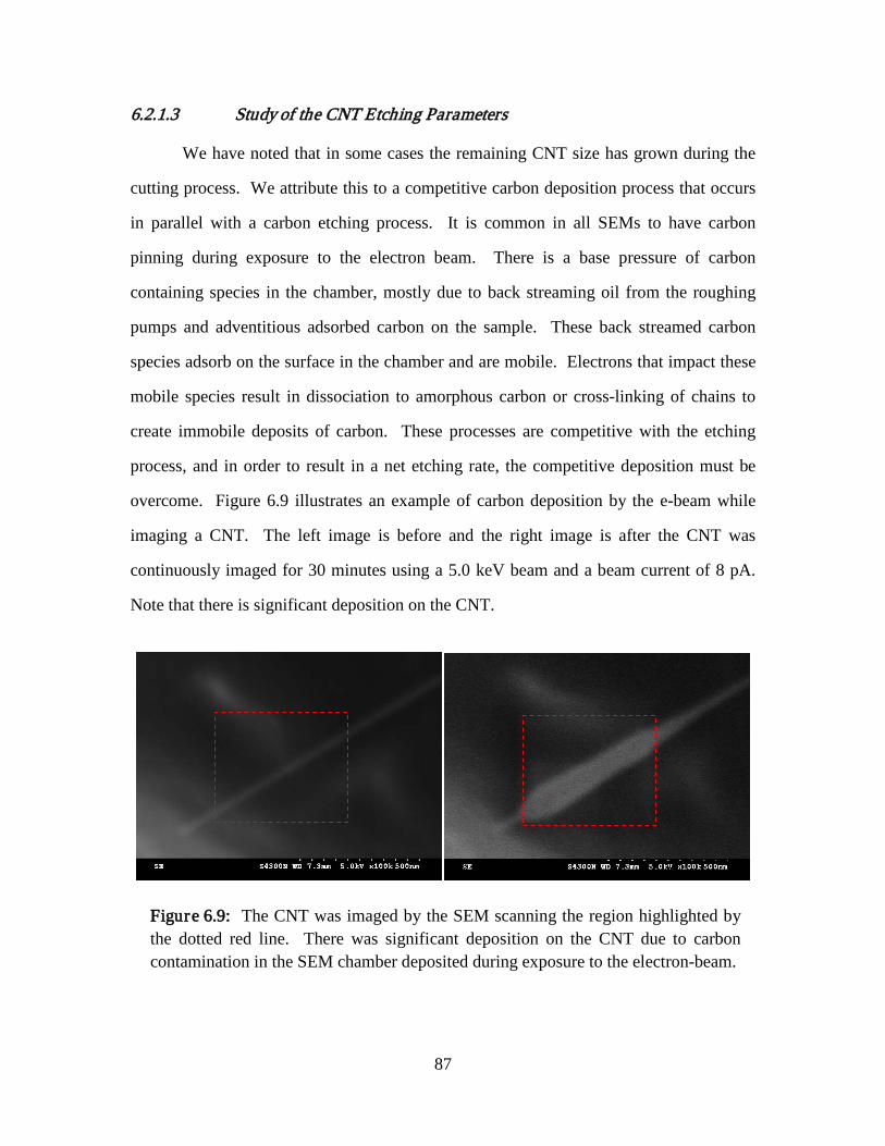
87
6.2.1.3 Study of the CNT Etching Parameters
We have noted that in some cases the remaining CNT size has grown during the
cutting process. We attribute this to a competitive carbon deposition process that occurs
in parallel with a carbon etching process. It is common in all SEMs to have carbon
pinning during exposure to the electron beam. There is a base pressure of carbon
containing species in the chamber, mostly due to back streaming oil from the roughing
pumps and adventitious adsorbed carbon on the sample. These back streamed carbon
species adsorb on the surface in the chamber and are mobile. Electrons that impact these
mobile species result in dissociation to amorphous carbon or cross-linking of chains to
create immobile deposits of carbon. These processes are competitive with the etching
process, and in order to result in a net etching rate, the competitive deposition must be
overcome. Figure 6.9 illustrates an example of carbon deposition by the e-beam while
imaging a CNT. The left image is before and the right image is after the CNT was
continuously imaged for 30 minutes using a 5.0 keV beam and a beam current of 8 pA.
Note that there is significant deposition on the CNT.
Figure 6.9: The CNT was imaged by the SEM scanning the region highlighted by the dotted red line. There was significant deposition on the CNT due to carbon contamination in the SEM chamber deposited during exposure to the electron-beam.

88
Toth et al. [6.15] observed that deposition versus etching switching for a generic
gas species can be controlled by the electron flux. For either deposition or etching, the
rate of reaction is proportional (and limited by) to the flux of electrons, at low electron
flux, until the electron flux is sufficient to deplete the precursor gas coverage.
Afterwards, the rate becomes limited by the mass transport of new precursor to the
surface. This results in a constant rate of reaction for higher electron fluxes. In addition,
at low electron fluxes, the deposition process is more efficient than the etching process
due to a higher dissociation probability of the carbon deposition precursor than the
dissociation probability of the water. As electron flux increases, the deposition process
becomes mass transport limited by the arrival rate of deposition precursor. Provided that
there is a sufficiently high pressure of etch precursor; as electron flux continues to
increase, the etch process rate continues to increase in proportion to the electron flux.
The etching process then becomes more efficient than the deposition and net etching
results (Figure 6.10 – left). The net etching rate can be improved by removing the source
of hydrocarbon contamination. This lowers the deposition rate enabling a larger net
etching rate (Figure 6.10 – right). Increasing the local water pressure increases the gas
coverage on the surface resulting in a higher etching rate, improving the net rate towards
etching (Figure 6.11 – right). As illustrated in Figure 6.11, the etching rate can also be
improved by cleaning volatile carbon containing species out of the SEM chamber (Figure
6.11 – right), increasing as much as possible the precursor pressure at the CNT surface,
and increasing the electron flux as high as possible.

89
Carbon containing species can be removed from the SEM chamber by the use of
an oxygen plasma source (in our case an EVACTRON™ cleaning system from XEI
Scientific, Inc). The system supplies low power RF plasma to atmospheric gases leaked
into the chamber through a metering valve. The low power plasma provides enough
power to ionize and dissociate O2 but not enough to ionize N2. This provides a supply of
oxygen radicals to the chamber. We used a power setting of 14 W forward RF power and
a pressure of 0.4 Torr (~53 Pa) to maximize the creation of oxygen radicals. The oxygen
radicals react with the mobile carbon-containing species in the chamber, forming carbon
monoxide, carbon dioxide, water, and hydrogen molecules. These volatile gas species
Figure 6.11: Deposition rate, etching rate, and net rate versus increasing electron flux
Figure 6.10: Deposition rate, etching rate, and net rate versus increasing electron flux

90
are subsequently pumped from the chamber by the vacuum system. The result is the
removal of species from that chamber that lead to unwanted carbon deposition.
We varied the SEM chamber plasma cleaning time followed by cutting a single
CNT in multiple places. The procedure was to vent the SEM chamber to atmosphere,
open the chamber doors, and leave the chamber at atmosphere for 1 hour. The system
was then pumped to a base pressure of 5.0×10⁻⁴ Pa and the beam was set to a 100 pA
current at beam energy of 20 keV. The CNTs were cut at a chamber background pressure
of 2.0×10⁻² Pa of water, with the exception of the control run with zero water flow and a
chamber background pressure of 5.0×10⁻⁴ Pa. The cutting time was 120 sec or CNT cut
endpoint, whichever came first. The images of the processed CNTs are shown in Figure
6.12. For the control, a net deposit was observed due to the carbon contamination in the
SEM chamber. With little or no cleaning, the competitive deposition was not overcome
by the etch process, and a net deposit was observed. With sufficient cleaning time the
CNT was able to be cut. For plasma cleaning of about 2 minutes or more the net reaction
was etching.

91
We investigated the electron flux influence on the etching rates with an
experiment in which the beam current was changed by adjusting the SEM condenser lens,
while the limiting aperture and working distance remained constant. The background
pressure was also maintained constant at 2.0×10⁻² Pa. The time to cut a nanotube was
observed by the end point of the secondary electron image during etching and the etch
rate was calculated by dividing the diameter of the CNT by the time to cut. The results
from this etching are plotted in Figure 6.13 below. We observed that the etch rate
improved with increasing probe current. We assume that the probe size is diffraction
limited and therefore the peak electron flux is proportional to the beam current. In this
Figure 6.12: RF plasma cleaning time vs. net etching/deposition experiment

92
assumption, it is seen that the etching is electron flux limited, that is the reaction rate
increases in proportion to electron flux and does not fully reach a mass transport limited
regime. That is not to say that under a fixed beam a mass transport rate limited regime
would not occur, but rather that here the scanning rate is fast enough that the precursor
does not deplete during the beam dwell time. Also, it should be noted that these CNTs
were cut in a chamber that had been thoroughly cleaned of hydrocarbon contaminants.
A more complete full factorial experiment was conducted to investigate the
effects of beam current, beam energy, and plasma cleaning time. The experimental
parameter space was as follows:
Beam Energy – 1=5 keV, 2=12.5 keV, 3=20 keV
Beam Current – 1=10 pA, 2=45 pA, 3=80 pA
Cleaning Time – 1=4 min, 2=20 min
The main effects are plotted in Figure 6.14. The results indicate that all three
parameters are statistically significant. It can be observed that the beam current and
cleaning time have strong linear effects. As expected, increasing the beam current
Figure 6.13: CNT etch rate versus beam current
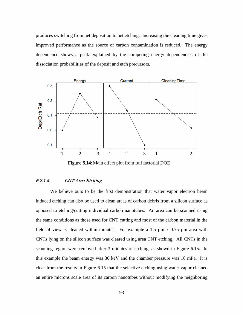
93
produces switching from net deposition to net etching. Increasing the cleaning time gives
improved performance as the source of carbon contamination is reduced. The energy
dependence shows a peak explained by the competing energy dependencies of the
dissociation probabilities of the deposit and etch precursors.
6.2.1.4 CNT Area Etching
We believe ours to be the first demonstration that water vapor electron beam
induced etching can also be used to clean areas of carbon debris from a silicon surface as
opposed to etching/cutting individual carbon nanotubes. An area can be scanned using
the same conditions as those used for CNT cutting and most of the carbon material in the
field of view is cleaned within minutes. For example a 1.5 µm x 0.75 µm area with
CNTs lying on the silicon surface was cleared using area CNT etching. All CNTs in the
scanning region were removed after 3 minutes of etching, as shown in Figure 6.15. In
this example the beam energy was 30 keV and the chamber pressure was 10 mPa. It is
clear from the results in Figure 6.15 that the selective etching using water vapor cleaned
an entire microns scale area of its carbon nanotubes without modifying the neighboring
Figure 6.14: Main effect plot from full factorial DOE
1 2 3 1 2 3 1 2

94
nanotubes. Figure 6.16 shows before and after images of an area cleaned by selective
CNT etching. The area inside the red dotted lines was scanned for 10 minutes, and then
the wider (after cleaning) image on the right was captured to show that the non-scanned
areas are not affected. Large CNTs in the field of view remain, as they would require
longer exposure times to etch under these conditions. Alternatively, larger aperture
settings could be used to increase the current beyond the ~ 1.2 nA which was used in this
experiment.
Pre-clean Post-clean
Figure 6.15: 1.5 µm x 0.75 µm area CNT etching with water vapor precursor. It is clear that the etching using water vapor cleaned an entire microns-scale area of its carbon nanotubes without modifying the neighboring nanotubes.
Figure 6.16: Before (left) and after (right) area cleaning
95
6.2.2 Exper imental Setup II
6.2.2.1 Demonstration of improved CNT cutting efficiency
The CNT cutting process needs to be efficient and fast to support rapid CNT
editing. The initial results have shown that for a fixed CNT etching rate the etching
efficiency depended on the electron beam energy, the beam current, and the precursor
pressure (the water vapor partial pressure). These findings were also reported by others
[6.12]. These results show that higher precursor pressures lead to higher CNT etching
efficiency. The local precursor pressure, at the sample, and not the average chamber
pressure (background pressure) determines the precursor flux and therefore the CNT
etching. Then the question becomes, can the optimal precursor pressure be easily
achieved and adjusted? The precursor flux as given by the kinetic theory of gases is:
Γmol = P√2 π m k T
moleculess−m2 (Eq. 6.1 repeated from above)
where P is the local precursor pressure, m is the molecular mass, k is Boltzmann’s
constant, and T is absolute temperature. We can easily measure the average chamber
pressure but it is impossible to directly measure the localized precursor pressure at the
sample. Localized precursor pressure however can be computed by knowing the
chamber pressure and the gas nozzle geometry. We measured the optimal precursor
pressure to be 1−2 ×10⁻² Pa, very close to the upper operating limit of most SEMs. A
higher precursor pressure would increase the CNT etching efficiency but it would also
require the use the SEM instrument in an environmental mode, an expensive and more
complicated SEM option.
Therefore, we investigated whether the CNT etching efficiency can be increased
by increasing the local precursor pressure and flux but without increasing the chamber
pressure. This was achieved by modifying the design of a conventional gas
injection/delivery system, and in particular enabling better control of the nozzle-sample
distance. We expected that when we decreased the nozzle-sample distance we would
achieve higher localized precursor pressure and flux while maintaining lower chamber

96
pressure. Because the gas flow from a nozzle spreads in a spatial cone, for a fixed gas
flow the pressure (force over unit area) and the flux (flow over unit area) will increase for
decreased nozzle-sample distance. Then, due to the high pressure gradient, the
background pressure will be maintained low. With this approach we planned to achieve
optimal localized precursor pressure and flux at chamber pressures of less than 1×10⁻² Pa,
and in the range of 10-3 to 10-4 Pa.
6.2.2.2 Experimental Setup II
The localized precursor pressure experiments were carried out in a Hitachi S-4000
non-environmental SEM with custom built gas delivery/injection system. The purpose of
the gas delivery system was to leak water vapor gas to the sample inside the SEM. The
gas delivery system consisted of components internal to the SEM and components
external to the SEM, as shown in Figure 6.17. The liquid water precursor was stored in a
special stainless steel reservoir with a shut off valve that could be detached from the rest
of the system and refilled with water as needed. Form the reservoir to the vacuum
chamber the gas delivery takes place through a ¼ inch stainless steel tube and has two
needle valves (which can also stop the flow) connected in series. We selected two valves
to better control the gas flow. The vacuum feedthrough has ¼ inch SwagelokTM
connections on both sides of the flange. The two valves are connected on the external
side. On the inside, the ¼ inch tube is reduced to a ⅛ inch size and is connected to a ⅛
inch PTFE flexible tube using SwagelokTM connections. We used Gauge 20 PTFE tube
with 12 inches of length for the gas delivery inside the SEM. Gauge 20 had 1.68 mm OD
and 0.86 mm ID. The ID and the length of the tube were selected to allow gas
conductance from the source to the needle but at the same time to be evacuated by the
SEM vacuum in a short time period after the gas flow is stopped by the valves. The
SwagelokTM was selected to allow testing of different tube sizes and lengths.

97
A Gauge 26 metal needle acting as a gas nozzle was epoxied at the far end of a
plastic delivery tube. The Gauge 26 needle had 460 μm OD and 254 μm ID. The plastic
delivery tube and the needle were connected to the boom of a nanomanipulator with the
needle extending from the end of the boom so as to be able to come in close proximity to
the sample. For this investigation the nozzle angle (the angle between the sample and the
centerline of the nozzle) was 0° so as to allow close positioning of the nozzle to the
sample. With the help of the nanomanipulator the nozzle could be placed from 1 mm to
50 μm with respect to the sample. This capability was the essence of our design and the
localized pressure experiments. The system used in these experiments was the bases for
a commercial product, Parallel Gas Injection System (PGIS) [6.16], developed by Xidex
Corporation.
We determined the conductance limited throughput of our gas delivery system by
opening all the valves of the system all the way to the water reservoir and determining the
maximum equilibrium pressure that was reached. Our SEM can routinely reach a base
pressure of about 2×10⁻⁷ Torr with overnight pumping. During the day and with opening
the main chamber the base pressure is about 2×10⁻⁶ Torr. The base pressure obtained for
the latest gas delivery system, when the valves were fully open was 5.5×10⁻⁵ Torr. This
pressure was stable after many hours of operating the SEM. Upon closing all the valves
of the gas delivery system the chamber pressure returned to below 1×10⁻⁶ Torr in 20−25
minutes. Quick evacuation of the gas delivery tubes makes the system practical for
everyday operation.

98
6.2.2.3 Relationship between the nozzle-sample distance and the localized precursor pressure
We demonstrated improved etching of carbon nanotubes and correlated it to the
small distance between the nozzle and the sample. We therefore observed that the small
distance between the nozzle and the sample results in the increase of the localized gas
pressure which in turn is responsible for the improved etching of carbon nanotubes.
Because it is impossible to directly measure the localized precursor pressure at the
sample, the local pressure can be computed by knowing the chamber pressure and the gas
nozzle geometry. Details of this computation are described by Kohlmann et al. [6.8].
We first conducted tests to check if the presence of a needle 100s of microns in
size in close proximity to the sample would distort the SEM image and make it
impossible to image the nanotubes, therefore making this approach infeasible. We ran
Figure 6.17: Electron beam induced etching system with novel nanomanipulator based gas delivery/injection system.

99
initial tests by moving the needle from 1000 μm to 50 μm away from the sample and by
imaging with high resolution (35 kx and above) on the very same CNT sample. These
runs revealed that the gas delivery needle had to be electrically grounded for this
approach to work. We discovered that the grounding had to have resistance of less than 1
kΩ to be effective. This was achieved by clipping an alligator clip to the needle and
grounding it via a short length of hook-up wire to the SEM walls.
We introduced the gas into the chamber through the nozzle, with pressures in the
range of 1−5×10⁻⁵ Torr. The presence of the gas introduced a gas ionization that was
observed via electron imaging. Figure 6.18 shows the visualization of the water vapor
flow from the nozzle as the nozzle-sample gap was reduced. We explain the flow lines as
result of the electron beam induced ionization of the water molecules. We used the flow
streamlines to estimate the gas spread angle β, as defined by Kohlmann et al. [6.8]. The
average spread angle was estimated to be 34°. The results of the tests show that with this
SEM we could not image well the CNTs at beam energies of more than 20 keV but CNT
imaging was fine for lower beam energies. The larger beam energies also introduced
sample charging and drift. Effective CNT etching requires stable imaging for several
minutes at high magnification.

100
The next question we had to answer was at what instrument settings CNTs could
be etched. We investigated beam energies of 20 keV, 10 keV, and 5 keV. The highest
beam energy also produced the largest sample currents, in the range of 1−2 nA, but
resulted in no CNT etching. At medium beam energy the sample currents were in the
range of 120 pA but also resulted in no CNT etching. The most effective was the beam
energy of 5 keV. We were able to cut CNTs with modest sample currents of 10−80 pA,
as shown in Figures 6.19 and 6.20. Although the etching process is slower for low
currents, one benefit of the low currents was that the etching process is more selective.
For example, Figure 6.19 shows a full cut to the middle CNT but the large CNT to the
left and the CNT to the right are only partially cut. Similarly, Figure 6.20 shows a full
cut to the right CNT but a partial cut to the CNT on the left.
Testing the selective CNT cutting of larger nanotubes was more difficult and
resulted in partial CNT cuts. Figure 6.21 shows partial cutting of a 90 nm thick CNT, at
5 keV beam energy, 120 pA sample current, and 3×10⁻⁵ Torr chamber pressure. After 14
Figure 6.18: Visualization of the water vapor flow from the nozzle as the nozzle-sample gap was reduced. The gas spread angle β is estimated from the streamlines.
a) b)
c) d)
476µm 456 µm
356 µm 296 µm
β=29° β=31°
β=34° β=42°

101
minutes the CNT was still not cut but closer examination shows that there was a split
(hole) made in the CNT as a result of the CNT etching. The splitting of the CNT was not
expected but it may be used in future for more advanced CNT studies.
It is clear from the results in Figure 6.21 that the selective etching using water
vapor cleaned entire microns size area of its carbon nanotubes without modifying the
neighboring nanotubes.
a) b) c)
Figure 6.19: Selectively cutting a CNT at low sample currents (10−80 pA), before (a) and after (b). Note that the large CNT to the left and the CNT to the right are only partially cut.
b) a)
Figure 6.20: Selectively cutting a CNT at low sample currents (10−80 pA), before (a) and after (b). Note that the CNT to the left is only partially cut.
b) a)

102
The SEM current was controlled with the Condenser Lens and the Lower
Aperture. With currents of less than 10 pA we could not etch a CNT in a reasonable time
of less than 4 minutes. A summary of the beam energies, currents, and SEM settings we
investigated are provided in Table 6.1.
Table 6.1: Summary of the investigated beam energies, currents, and SEM settings
Beam (keV)
Sample Current (pA)
Condenser Lens
Aper ture CNT Etching
20 1000 to 2000 3 1 did not cut any CNT
10 120 3 1 did not cut CNTs in 4 min or less
5 10 to 80 3 1 cut most CNTs
5 30 5 1 can cut CNTs
5 8 5 2 did not cut CNTs in 4 min or less
5 3 9 2 did not cut CNTs in 4 min or less
Next we investigated the relationship between the nozzle-sample distance and the
etching time and rate. The tests were conducted with beam energy of 5 keV and average
chamber pressure of 5.2×10⁻⁵ Torr. We measured the etching time 𝜙𝜙𝑒𝑒𝜙𝜙𝑐𝑐ℎ and the sample
current. The etching time was recorded as the time interval from the beginning of the
Figure 6.21: Partial (non complete) cutting of a 90 nm diameter CNT, before (a), after 14 minutes of etching (b), and a split in the CNT diameter due to the partial cutting (c).
a) b) c)

103
electron beam scan until the CNT was completely cut, as shown in Figure 6.4 and
described in the associated text. The experimental etching rate was computed by dividing
the size of the etched CNT, which had an average diameter of 25 nm, with the etching
time: 𝐸𝐸𝜙𝜙𝑐𝑐ℎ 𝑅𝑅𝑎𝑎𝜙𝜙𝑒𝑒 = 𝑎𝑎𝑐𝑐𝑎𝑎𝜙𝜙
𝜙𝜙𝑒𝑒𝜙𝜙𝑐𝑐 ℎ (Eq. 6.5)
For this experiment we changed the needle-sample distance from 87 μm to 328
μm by doubling the gap with each iteration, and then we returned back to the smallest gap
we could use for that sample, 76 μm, to verify that we were not building up some bias.
Figure 6.22 shows the result of this trial. To be consistent, all CNT cuts were done on the
same multi microns long carbon nanotube where each cut was few microns away from
the other. For a gap of 164 μm we can see that the CNT was cut in a segment. During
these experiments we also kept the magnification the same for all trials, at 35 kx for
imaging and 100 kx during etching. Table 6.2 lists all the parameters for this experiment.
Table 6.2: Summary of the experimental results measuring etch rate as function of the nozzle sample distance.
Gap
(μm)
Sample
Current (pA)
Etch
Time (sec)
Etch
Rate (nm/sec)
76 15 55 -0.457
87 10 110 -0.228
164 20 170 -0.148
328 30 230 -0.109

104
Gap (μm)
Gap Image CNT Before Cut CNT After Cut
76
87
164
328
Figure 6.22: Demonstration of gas delivery system fixed to a nanomanipulator that allows precise positioning of the gas nozzle to the sample with a rage of 50 μm to 1 mm and more. The resulting nozzle proximity results in improved CNT etching capabilities.
One important conclusion for this experiment is that the etching time and rate
improved for a smaller gap between the sample and the nozzle, as shown in Figure 6.23.
We also observed a trend that for a smaller gap the probe current decreased, as shown in
Figure 6.24. We interpret the change in the probe current as a function of distance as
being due to ionization and competitive positive current flow which increases with
decreasing spacing because of the enhanced local pressure. Because the smaller nozzle
distance shows faster etching rates and lower sample currents, the results from Figures

105
6.23 and 6.24 lead to a conclusion that the local pressure is responsible for the increased
etching rate.
The benefits of achieving optimized localized precursor pressure and flux at
reduced chamber pressures are multiple. First, the higher optimized localized precursor
pressure will result in better CNT etching efficiency and therefore in faster etching times.
Furthermore, at desired optimized localized precursor pressures the chamber pressure
will be lower, increasing the lifetime of the SEM filament and decreasing the
maintenance of the SEM tool, and in particular the ion pumps. The lower chamber
pressure also means that the CNT etching can be practiced in simpler less-expensive non-
environmental SEMs. Finally, operating the SEM at lower chamber pressures means less
gas scattering and therefore less beam spread, resulting in more precise beam operation.
6.2.2.4 Cantilevered CNT Etching
We also demonstrated that the more efficient carbon nanotube etching, with
optimized localized precursor pressure, works for free standing (cantilevered) carbon
nanotubes. Figure 6.25 shows the process of cutting two free standing CNTs with
different diameter. After an initial etching attempt the thinner CNT was completely
etched away while the thicker CNT was unchanged. It is also possible that the smaller
Figure 23– Demonstration of improved CNT etching time (etching rate) vs. nozzle-
sample distance.
Figure 24 – Probe current vs. nozzle-sample distance.
507090
110130150170190210230250
50 100 150 200 250 300 350
Nozzle-Sample Gap (µm)
Etch
Tim
e (s
ec)
Figure 6.23: Demonstration of improved CNT etching time (etching rate) vs. nozzle-sample distance.
0
5
10
15
20
25
30
35
50 100 150 200 250 300 350
Nozzle-Sample Gap (µm)
Prob
e C
urre
nt (p
A)
Figure 6.24: Probe current vs. nozzle-sample distance.

106
CNT did just bend away. After some additional etching time the thicker CNT was bent
and deformed but it was not cut. Figure 6.26 shows another free standing CNT that was
successfully shortened using localized CNT cutting, demonstrating the utility of our
method to edit even free standing CNTs. The tests were conducted with beam energy of
5 keV, sample current of 100 pA, and chamber pressure of 1×10⁻⁵ Torr. The nozzle-
sample distance was measured to be 75 μm. The difficulty of cutting free standing CNTs
without a surface in the background is associated with the lack of secondary and
backscattered electrons which reduces the electron flux available for etching. This
explains the need to operate at higher beam currents when cutting free standing CNTs.
For equivalent conditions (beam energy of 5 keV, nozzle-sample distance of 75 μm,
average chamber pressure of 1-5×10⁻⁵ Torr) the CNT laying on the surface required only
15 pA of beam current to cut (see Table 6.2) while the required beam current for cutting a
free standing CNT was 100 pA, a 7X more beam current. Another difficulty with editing
free standing CNTs is the lack of tension to hold the CNT steady under the electron beam
line scan. Double suspended CNTs and CNTs laying on a surface both have the required
tension. Figure 6.25 shows how the CNT gets deformed and bend without the presence
of CNT tension.
a) b)
Figure 6.25: (a) shows two free standing CNTs with different diameter. After an initial etching attempt the thinner CNT was completely etched away while the thicker CNT was unchanged (b). After some additional etching time the thicker CNT was bent and deformed but it was not cut (c).
b) a) c)

107
6.2.2.5 Application of the CNT Etching on a F ield Emission Device
We demonstrated carbon nanotube etching process that works for editing of a
carbon nanotube based device that we fabricated. In particular, we demonstrated
utilization of the selective CNT etching process for editing a lateral (horizontal) CNT-
based device like the one shown in Figure 6.27. Figure 6.28 shows the result of using
selective CNT etching to remove an extra CNT extending from a silicon post to the
substrate. The ability to remove excess CNTs (which are there due to the imperfections
of the growth process) is critical for CNT based prototype development because such
excess CNTs can result in unwanted operation or otherwise interfere with electrical or
mechanical device performance.
Figure 6.26: A free standing CNT, before (a) and after its length was shortened (b) using localized CNT cutting.
a) b)
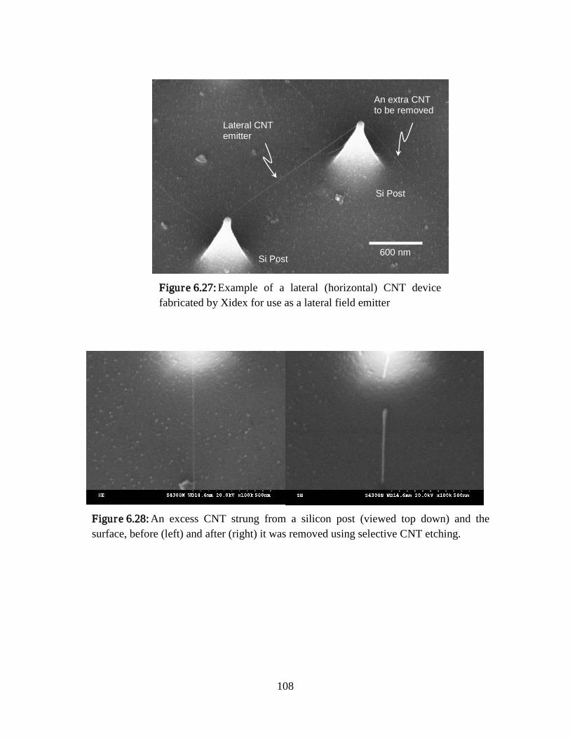
108
Figure 6.27: Example of a lateral (horizontal) CNT device fabricated by Xidex for use as a lateral field emitter
An extra CNT to be removed
Lateral CNT emitter
Si Post
Si Post
600 nm
Figure 6.28: An excess CNT strung from a silicon post (viewed top down) and the surface, before (left) and after (right) it was removed using selective CNT etching.

109
6.2.2.6 Modeling of the CNT Cutting Process
A continuum model developed by our collaborators at The University of
Tennessee, at Knoxville [6.17], is used to model the etch rate of the CNT. The rate
equation for the precursor gas concentration is: 𝑎𝑎𝐶𝐶𝐴𝐴𝑎𝑎𝜙𝜙
= 𝑔𝑔 𝛤𝛤𝑚𝑚𝑆𝑆𝑙𝑙 1 − 𝐶𝐶𝐴𝐴𝑧𝑧 − 𝐶𝐶𝐴𝐴
𝜏𝜏𝐴𝐴− 𝐴𝐴𝜎𝜎 𝛤𝛤𝑒𝑒 𝐶𝐶𝐴𝐴
𝑧𝑧 (Eq. 6.6)
Where 𝐶𝐶𝐴𝐴 is the precursor gas concentration, 𝑔𝑔 is the sticking coefficient, 𝛤𝛤𝑚𝑚𝑆𝑆𝑙𝑙 is
the molecular flux on the surface (also the molecular impingement rate), Z is the surface
adsorption site density, 𝜏𝜏𝐴𝐴 is the surface residence time of the precursor gas molecule,
𝐴𝐴𝜎𝜎 is the probability of electron induced dissociation, and 𝛤𝛤𝑒𝑒 is the electron flux. The
steady state solution for the etching rate is: 𝐸𝐸𝜙𝜙𝑐𝑐ℎ 𝑅𝑅𝑎𝑎𝜙𝜙𝑒𝑒 ∝ 𝜒𝜒 𝐴𝐴𝜎𝜎 𝛤𝛤𝑒𝑒 𝑔𝑔 𝛤𝛤𝑚𝑚𝑆𝑆𝑙𝑙
𝑔𝑔 𝛤𝛤𝑚𝑚𝑆𝑆𝑙𝑙 + 𝑍𝑍𝜏𝜏𝐴𝐴
+𝐴𝐴𝜎𝜎 𝛤𝛤𝑒𝑒 (Eq. 6.7)
Where 𝜒𝜒 is the stoichiometry factor relating the number of etch product molecules
generated per precursor molecules consumed. The surface residence time can be
calculated from:
𝜏𝜏𝐴𝐴 = 1𝜈𝜈𝑒𝑒𝐸𝐸𝑎𝑎𝑎𝑎𝑣𝑣𝑘𝑘 𝐶𝐶 (copy of Eq. 6.3)
Where 𝜈𝜈 is the fundamental vibrational frequency on the order of 1013 s-1. Using
a published value of the energy of adsorption for water on carbon nanotubes of ~30
kJ/mol, we arrive at a surface residence time about 15 nanoseconds. If we assume a site
density around 1015 cm-2, then the middle term of the denominator in the etch equation
(Z/τA) is around 6.4×1022 cm-2 s-1. The pressure of water in the chamber is 2.0×10⁻² Pa,
this corresponds to a molecular flux (molecular impingement rate) of around 9.6×10¹⁶
cm-2s-1. Even using a sticking coefficient of 1.0, the first term in the denominator is very
small compared to the second term, and so it can be ignored. Calculating a peak electron
flux of about 8.5×1021 cm-2s-1 for a 1 nA beam at 20 keV, the third term (Aσ Γe) is about
an order of magnitude or more less (depending on Aσ) than (Z/τA), so the etch rate
equation can be simplified to:

110
𝐸𝐸𝜙𝜙𝑐𝑐ℎ 𝑅𝑅𝑎𝑎𝜙𝜙𝑒𝑒 ∝ 𝜒𝜒 𝐴𝐴𝜎𝜎 𝛤𝛤𝑒𝑒 𝑔𝑔 𝛤𝛤𝑚𝑚𝑆𝑆𝑙𝑙𝑍𝑍𝜏𝜏𝐴𝐴
= 𝜒𝜒 𝐴𝐴𝜎𝜎 𝛤𝛤𝑒𝑒 𝑔𝑔 𝛤𝛤𝑚𝑚𝑆𝑆𝑙𝑙 𝜏𝜏𝐴𝐴 𝑍𝑍
(Eq. 6.8)
Therefore, the etch rate is proportional to the electron flux, the molecular flux,
and the surface lifetime of the precursor gas molecule. Increasing the beam current by
passing more current through the limiting aperture with the condenser lens makes the
probe shape become brightness limited, and further increases to current do not increase
the peak electron flux, but rather the width of the beam. Assuming a maximum electron
flux of 1×1023 cm-2s-1, a simulation of etch rate versus impingement rate follows. Using
Eq. 6.8, simulated results of the effect of molecular flux (and with it the localized
pressure via Eq. 6.1) on the etching rate are shown in Figure 6.29. As can be observed,
as the molecular flux (localized pressure) increases, the etch rate increases. The
simulation reveals that it would be desirable to design a system that operates at a higher
localized pressure in order to increase the gas coverage of water and thus increase the
etching rate. This follows the observed experimental behavior.
1012 1013 1014 1015 1016 1017 1018 1019 1020 1021 10221010
1011
1012
1013
1014
1015
1016
1017
1018
1019
1020
Molecular Impingement Rate (cm-2s-1)
Etc
h R
ate
(cm
-2s-1
)
Effect of Pressure on the Etching Rate
Figure 6.29: Effect of pressure on the etching rate

111
6.3 SUMMARY AND CONCLUSIONS
We tested the workspace of the relevant electron beam parameters by determining
their role in the electron-beam-based carbon nanotube etching process. In particular, we
tested the beam current and the beam energy at fixed scanning rates and fixed precursor
parameters (pressure and precursor gas). The results indicated that both electron beam
parameters are significant. We observed that the etch rate improves with increasing beam
current. However, we found that the energy dependence shows a quadratic effect that
likely is explained by the energy dependence of the dissociation probabilities of the
deposition and etch precursors.
The scanning parameters were also investigated. It was found that we needed a
short e-beam dwell time to keep a proper balance between the precursor molecule refresh
rate and the beam current. TV scan rates, 30 loops per second in a line scan mode, were
found to be nearly optimal. For the pressure range used in our experiments the precursor
sticking (gas coverage on the surface) was minimal which did not allow enough
sensitivity for us to perform a more detailed investigation of the scan parameters.
Therefore, the options we had available for improving the CNT etching efficiency
were the electron beam energy and current. Optimized carbon nanotube etching required
20 keV beam energy or higher at beam currents of 100 pA or more and TV scan rates of
imaging. Electron beam energy and current are functions of the SEM instrument and can
be optimized within the available limited ranges of the tool. However the localized
precursor pressure parameter can be more easily adjusted.
We observed the effects of varying the localized precursor pressure and flux. The
background pressure range was from 5.0x10⁻⁴ Pa (the base pressure without any
precursor gas) to 2.0x10⁻² Pa. The best pressure was found to be the maximum SEM
chamber pressure 2.0x10⁻² Pa with the precursor injected into the chamber by a needle
approximately 1 mm above the sample. Simulation of the gas flow indicates that the
local pressure at the surface under the injection needle is 10-100 times the background

112
pressure in the chamber. Higher background pressure is desired. However, it would have
required operating the SEM in an environmental mode, which would have introduced
imaging complications. Lower background pressures resulted in net deposition on the
carbon nanotubes instead of net etching.
Our results have shown that higher local precursor pressure (the molecular partial
pressure) requires less electron beam current and electron beam energy to achieve the
same CNT etching efficiency. Therefore, it is desirable to increase the CNT etching
efficiency by increasing the local precursor pressure and flux but without increasing the
chamber pressure. This was achieved by decreasing the nozzle-sample distance to below
100 μm by using a nozzle on a nano-manipulator approach to achieve higher localized
precursor pressure and flux while maintaining lower chamber pressure. Because the gas
flow from a nozzle spreads in a spatial cone, for a fixed gas flow the pressure (force over
unit area) and the flux (flow over unit area) increased for decreased nozzle-sample
distance.
We demonstrated a versatile carbon nanotube process that works for different
carbon nanotube samples. We demonstrated cutting of individual and multiple carbon
nanotubes, and we demonstrated line cutting and area cutting (cleaning) of carbon
nanotubes. Furthermore, we investigated the difference between CNTs lying on a surface
and CNTs protruding from the surface, as well as doubly supported CNTs (as opposed to
free standing cantilevered CNTs). We found that it was more efficient to etch CNTs
lying on the surface and to etch doubly supported CNTs than it was to etch free standing
(cantilevered) CNTs.
We investigated the cutting time as a function of carbon nanotube diameter. We
found that the time to cut the tube varies roughly linearly with the beginning size of the
tube. Typical cutting time ranged from 40 to 400 sec for CNTs with diameters ranging
from 15 to 35 nm.

113
It is common in all SEMs to have carbon deposition during exposure to the
electron beam and this creates immobile deposits of carbon on the CNTs (the samples).
The carbon deposition process is competitive with the etching process, and in order to
result in a net etching rate, the competitive deposition must be overcome. Increasing the
beam current, energy, pressure and flux all contribute to increasing the etching rate and
reducing the etching time. In addition, we developed a new pre-etching procedure that
improves the efficiency of the CNT etching process. In this procedure the SEM chamber
and the CNT samples are cleaned with oxygen plasma to remove carbon-containing
species from the SEM chamber and the sample itself. A full factorial experiment was
conducted to investigate the effects of the plasma cleaning time together with the beam
current and energy. Increasing the cleaning time improves the etching performance as
the source of carbon contamination is reduced.
We demonstrated that the etching time and rate improved for a smaller gap
between the sample and the nozzle. Because the smaller nozzle distance shows faster
etching rates and lower sample currents, the results lead to a conclusion that the local
pressure is responsible for the increased etching rate and not the sample current.
We designed and built an enhanced gas delivery system incorporated into a
nanomanipulator which enabled precise and close up gas delivery and successfully
operating the system in Hitachi S-4000 non-environmental SEM. Design of the enhanced
micro gas injection system was facilitated by experiments and modeling conducted using
an electron beam induced deposition and etching system located at the University of
Tennessee. With the help of another 3-axis nanomanipulator we anticipate doing more
complex experiments where one nanomanipulator is dedicated to a gas delivery system
and the other to manipulation or electrical or mechanical probing. For example, this
system can be used for fabricating and testing CNT emitters in a single SEM chamber
without exposing the CNT emitter to the atmosphere.
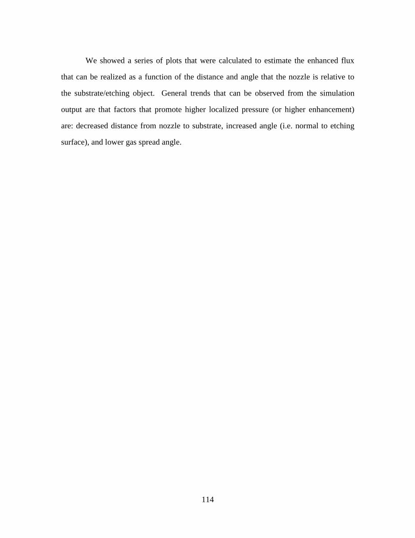
114
We showed a series of plots that were calculated to estimate the enhanced flux
that can be realized as a function of the distance and angle that the nozzle is relative to
the substrate/etching object. General trends that can be observed from the simulation
output are that factors that promote higher localized pressure (or higher enhancement)
are: decreased distance from nozzle to substrate, increased angle (i.e. normal to etching
surface), and lower gas spread angle.
115
Appendices
APPENDIX A: MANUAL FABRICATION OF A CARBON NANOTUBE TIP
This Appendix describes the procedure of how to manually fabricate a carbon
nanotube (CNT) tip on an atomic force microscopy (AFM) silicon (Si) based tip or on a
sharpened tungsten (W) tip. We describe the fabrication procedure using a commercially
available nanomanipulator from Xidex Corp., NanoBot NX-2000 (www.xidex.com), and
therefore use terminology unique to this instrument. However, the outlined fabrication
procedure can be accomplished using other commercial or custom made
nanomanipulators.
The described procedure was also recorded with a video and was posed on
YouTube (www.youtube.com/watch?v=Yefhs7vwToo).
A1 Introduction
A CNT manually attached to the end of a conventional silicon AFM tip, as shown
in Figure A1, enables scanning with higher spatial resolution and less tip wear than
would otherwise be possible. Use of a stable nanomanipulator, such as the NanoBot
system, offers exceptional ease of use and mechanical stability to make it possible to
quickly accomplish this difficult and meticulous nanofabrication task inside a scanning
electron microscope (SEM).
Figure A2 shows a NanoBot nanomanipulator, Model NX-2000, which has two
XYZ positioners, mounted on the door assembly of an SEM. This mounting option leaves
the SEM sample stage free for use in the nanofabrication process. Only one of the XYZ
positioners is required to fabricate a CNT AFM tip using the method described here.

116
A2 Sample Preparation
A CNT source and an AFM tip are mounted on a standard SEM sample holder
using SEM tape as shown in Figure A3. Multiple AFM tips can also be mounted this
way for batch fabrication. The CNT source is a silicon chip on which CNTs have been
grown using chemical vapor deposition (CVD). This sample was fabricated by Xidex
Corp.
Alternatively, a loose bundle of CNTs can be used as a source instead of a
substrate with grown CNTs. For example, the CNT source can be a razor blade with bulk
CNTs dispensed on its edge by running the blade into a powder of bulk CNTs. Bulk
CNTs can for example be purchased from Cheap Tubes Inc. (www.cheaptubesinc.com).
A sharp tungsten (W) tip is mounted on the NanoBot end effector, as shown in
Figure A4. The SEM door is then closed and the sample chamber is pumped down.
Figure A2: A NanoBot Model NX-2000 mounted on the door assembly of an SEM.
Figure A1: CNT manually attached to a Si AFM tip.
500 nm

117
A3 Picking Up a CNT with the W Tip
Nanomanipulator motion control in all three axes was accomplished with a
joystick interface. There are three modes of linear motion, each with a different level of
speed. The NanoBot’s Multi Step mode was used to rapidly maneuver the W tip in XYZ
toward the CNT source as shown in Figure A5. Multi Step mode enabled up to 15 mm of
XYZ travel. Both Multi Step mode and Single Step mode were used to maneuver the W
tip until it is within a few µm of the source of CNTs. Single Step travel was adjustable
from 100 nm to 2 µm. The CNT source was then examined by moving the SEM stage
until a straight CNT is found which is extending outward so that it can be easily accessed
as shown in Figure A6. This procedure typically requires only a few minutes. The
NanoBot system’s Fine Motion mode is then used to touch the W probe to the selected
CNT, as shown in Figure A7. The required high degree of mechanical stability is enabled
by the NanoBot system’s extremely low drift, on the order of 10 nm per minute, in all
Figure A4: Mounting of a sharp W tip on the NanoBot end effector.
Figure A3: AFM tip and CNT source
CNT Source
AFM Tip

118
three axes. The Fine Motion mode enables ± 3.5 µm of motion with 1 nm resolution in
XYZ. It normally takes about 30 seconds to bring the W tip into well oriented contact
with a selected CNT. Next, the CNT is welded to the W tip using electron beam induced
deposition (EBID) of carbon. In this procedure it is assumed that the SEM chamber is
somewhat contaminated with hydrocarbon. In the EBID procedure the magnification of
the SEM is set to about 100 kx so that the CNT-tip junction is in full view of the SEM
monitor, and the beam energy is set to 10 keV. After 30 to 60 seconds of imaging we
have actually deposited carbon from the SEM contamination and covered over the CNT
and W tip.
A4 Separating the CNT from the CNT Source
One way to separate the CNT from the CNT source substrate (as shown in Figure
A8), is to apply an electrical current pulse between the W probe and the substrate. In this
procedure we connected a Keithley 237 current-voltage source to the W probe and
electrically grounded the SEM holder. We then manually applied a current pulse of 1-5
µA to the W probe for 1-2 seconds, basically turning the power supply on and off
Figure A5: W tip approaching CNT source.
CNT Source
W Tip
Figure A6: W tip maneuvered to within a few µm of a CNT.
CNT Source
W Tip
CNT

119
immediately. More sophisticated electrical cutting can be accomplished by writing
LabView based code that turns on and off the power supply with 1 ms precision.
It has to be noted that the location of the CNT cutting using this procedure is not
very accurate because the CNT probably cuts at the location along the CNT where the
resistance is the highest due to possible defects in the lattice of the CNT molecule.
In the case where the CNT source consisted of loose bundle of CNTs (instead of a
substrate with grown CNTs), the CNT connected to the W tip could be pulled away from
the bundle without the need for electrical cutting.
This procedure completes the fabrication of a CNT tip on a sharp W probe. In
this work this was the procedure we used to manually fabricate CNT emitters on a sharp
W wire. The next few steps describe how to now manually mount the CNT to an AFM
tip.
A5 Attaching the CNT to the AFM Tip
The W tip carrying the CNT is rapidly translated in XYZ to within a few microns
of the AFM tip apex, as shown in Figure A9. The NanoBot system’s Fine Motion mode,
is then used to place the CNT along the side of the silicon AFM tip apex, as shown in
Figure A7: W tip in contact with the selected CNT.
W Tip CNT
CNT Source
Figure A8: CNT separated from substrate using current pulse.
W Tip
CNT

120
Figure A10. The dexterity of the NanoBot system makes it fairly easy to align the CNT
with respect to the AFM tip in XYZ. A reasonably well aligned CNT AFM tip (e.g., to ±
10º) can be made this way with some amount of practice. The CNT is welded to the AFM
tip using EBID of carbon. This procedure was described above.
A6 Cutting the CNT Away from the W tip
An electrical current pulse is then used to cut the CNT away from the tungsten tip
as shown in Figure A.11. This procedure was described above. The electrical cutting
procedure did not change because one of the substrates is Si, since the Si in the AFM tip
is highly doped and therefore conductive.
Figure A10: CNT placed along the side of the AFM tip.
Figure A9: W tip carrying CNT translated to within a few µm of the AFM tip.
AFM Tip W Tip
AFM Tip
W Tip CNT

121
A7 Alternative Procedures
Use of a sharp tungsten tip as an intermediate step, as described above, facilitates
selection and detachment of the CNT from its original substrate and also facilitates
attachment of the CNT to the AFM tip. Alternatively, a CNT can be attached to an AFM
tip in one step if the AFM chip was mounted on the end of the nanomanipulator.
However, this procedure may require more operator skill and can be complicated by the
presence of other CNTs in the vicinity of the CNT selected for mounting. If additional
batches of CNT tips need to be fabricated, they can be mounted on the SEM sample
holder by retracting and reinserting the load lock while the NanoBot carrying the W tip
remains in the sample chamber. This arrangement avoids the need to pump down the
chamber each time a new batch of CNT AFM tips is to be fabricated.
Figure A11: CNT separated from the W tip.
W Tip AFM Tip CNT Tip
Break

122
APPENDIX B: EVALUATING THE CONTACT RESISTANCE BETWEEN CARBON NANOTUBES AND W AND SI PROBE TIPS
This Appendix describes the characterization of the electrical properties of
conductive carbon nanotube (CNT) scanning probe microscope (SPM) tips. The project
results and conclusions were presented at SEMATECH’s AMAG/FMAG meeting in
Monterrey, California on February 20 & 21, 2008.
B1 Introduction
The objective of this work was to produce CNT SPM tips which are suitable for
nanometer scale measurement of carrier concentration profiles. The conductive CNT tips
for this project were fabricated using: direct growth of a single carbon nanotube on an
AFM silicon tip, manual mounting of a single carbon nanotube on an AFM silicon tip,
and manual mounting of a single carbon nanotube on a sharp W wire. These three
methods represent three alternative technologies for fabrication of CNT based tips.
Typical CNT diameter was less than 10 nm, and typical CNT lengths were 200 nm to
1000 nm but other lengths were feasible.
We electrically characterized CNT tips using current-voltage (I-V) measurements.
The main instrument used was Keithley 237 current-voltage source. The electrical
measurements were conducted while the samples were inside an SEM and right after they
were prepared. We used a nanomanipulator to assemble the samples and we used
electron beam induced deposition (EBID) of platinum to make electrical connections
between the CNTs and the probes. During this evaluation the CNT tip resistivity was
determined.
B2 Exper iments and Evaluation Procedures
We started our investigation by testing CNTs in contact to different substrates,
such as a W tip and a Si tip from an SPM cantilever. The main electrical characterization
test was by conducting I-V measurements.

123
The results from electrical characterization of a W tip connected to a single CNT
which has been grown on a Si substrate are shown in Figure B1. The CNT is connected to
the W tip via the Van der Waals force. The I-V curves for the assembled connection
(multiple runs) are shown in Figure B1-b. The large flat region from -4 to 4 V indicated
existence of a Schottky barrier resistance in the electrical circuit. Most probably the
Schottky barrier is between the W tip and the CNT but may also exist between the CNTs
and the Si substrate on which they were grown. The non-symmetry of the I-V curve
indicated that the results are from real Schottky barriers.
The results from electrical characterization of a CNT mounted on a W tip and in
contact with a Si tip via the Van der Waals force are shown in Figure B2. The I-V curves
are shown for the assembled W–CNT–Si Tip connection (Figure B2-b). Again, the flat
region from -4 to 4 V indicated an existence of a Schottky barrier resistance in the
electrical circuit. The measurement noise is better in this test (compared to the previous
test) because there is probably better contact between a single CNT and the W and Si
substrates with more of the CNT contacting both substrates.
Figure B1: Electrical characterization of W tip to a CNT nanowire grown on Si. a) SEM image of the physical connection, b) I-V curves from the electrical measurement.

124
Our next goal was to eliminate one of the substrates (the silicon) and observe the-
change in the I-V measurements. First we confirmed that a contact between two W tips is
very Ohmic and results in a linear I-V curve with resistance of few Ohms. Next, we
placed a CNT between the two W probes. The results from electrical characterization of
a single CNT connected between two W tips are shown in Figure B3. The CNT is
connected to both W tips via Van der Waals force. We repeated this procedure for two
different CNTs. The I-V curves for the assembled connection for both CNTs are shown
in Figure B3-b. The two curves are different due to the different CNT lengths and the
quality of their contact. We notice that the flat region in the I-V curve due to the
existence of a Schottky barrier resistance in the electrical circuit was reduced to less than
± 2 V, indicating that the dominant Schottky barrier in the previous measurements was
between the CNT and the Si substrate. Therefore, the remaining Schottky barrier was
due to the contact resistance between the CNT and the W.
Figure B2: Electrical characterization of W tip to a CNT tip manually attached to the W and the Si tip. a) SEM image of the physical connection, b) I-V curves from the electrical measurement.

125
The existence of the Schottky barrier resistance was expected but it does not
prevent the use of the CNT as an electrical probe. The consequence of having a Schottky
barrier is the increased bias voltage that has to be used for electrical measurements and
the additional deconvolution of the data after the electrical measurement. Nevertheless,
our next goal was to try to reduce the Schottky barrier resistance.
Therefore, in the next tests, we coated (welded) the contacts between the CNT
and its substrate. We used a localized e-beam deposition technique inside an SEM tool to
deposit Pt contacts to the CNT ends with nanometers precision. We repeated this test for
two different CNTs. Results showing the effect of Pt welding on electrical characteristics
of a W-CNT-W connection are shown in Figure B4. The I-V curves for the assembled
W-CNT-W connection with Pt welds are shown. The legend shows the following curves:
3 & 1 = CNT is connected to both W tips via Van der Waals force.
6 & 11 = Both CNT-to-W contacts were welded with Pt.
8 & 15 = The W tips and the CNT were covered with a thin layer of Pt.
Legends 3, 6, and 8 refer to a Sample 1 and legends 1, 11, and 15 refer to a
Sample 2. It can be seen that the resistivity of the circuit decreased after Pt welding of
the W-CNT contacts and the Schottky barrier was almost eliminated. It can be seen that
Figure B3: Electrical characterization of CNT manually attached to two W tips. a) SEM image of the physical connection, b) I-V curves from the electrical measurement.

126
even for a completely Pt coated CNT there are still nonlinearities in the IV curve. This
may be due to the non-complete coating process or due to the CNT wire resistance that is
now in parallel to the Pt wire resistance.
Better understanding of the results is possible if we normalize the results
accounting for the diameter and the length of the CNT. The resisitivity can be computed
as:
𝜌𝜌 = 𝑅𝑅 𝐴𝐴𝐿𝐿
1107 (Eq. B1)
where R is the measured resistance (Ω), L is the CNT length (m), A is the CNT
gross section area (m2), and 𝜌𝜌 is the resisitivity (Ω-cm).
The effect of Pt welding on probe resistivity is shown in Figure B5, where we
compare the probe resistivities before and after the Pt welding. The resistivity decreased
after welding the W-CNT contacts with Pt. For Sample 1 (Figure B5a), the average
resistivity dropped from 0.0335 to 0.0052 Ω-cm. For Sample 2 (Figure B5b), the average
resistivity dropped from 0.0152 to 0.0061 Ω-cm.
Figure B4: I-V results showing the effect of Pt welding (via electron induced precursor deposition) on electrical characteristics of a W-CNT-W connection. a) I-V curves for Sample 1 and b) for Sample 2.

127
Figure B6 shows the effect of Pt welding on the minimum resistivity of a W-CNT
contact. For Sample 1, minimum resistivity dropped down to 0.0058 Ω-cm. For Sample
2, minimum resistivity dropped down to 0.0037 Ω-cm. For comparison, commercially
available SPM probes for electrical measurements have resisitivities from 0.01 to 0.025
Ω-cm. In essence our probes are very conductive and compatible to or better than
existing electrical probes.
Figure B5: Comparative results showing the electrical characteristics of a W-CNT-W connection before (legend 3 and 1) and after Pt welding (legend 6 and 11). a) I-V curves for Sample 1 and b) for Sample 2.
Figure B6: Minimum resistivity of a W-CNT contact dropped after the CNT was welded to the W with Pt.

128
B3 Conclusions
We have measured the CNT-probe resistance on 20-30 CNTs as grown directly
on a Si substrate using I-V measurements. We recorded the overall measured resistance
R. Because each CNT had a different length and diameter we did not report the
resisitivity number. The typical CNT-probe resistance R was 500 kΩ and the minimum
measured CNT-probe resistance R was 30 kΩ. This is well above the theoretical CNT
resistance of a CNT which is 6.7 kΩ. We contribute the extra resistance to the contact
resistance between the CNT and the substrate. The minimum measured probe resistivity
ρ was 0.0037 Ω-cm. The resistivity of the conductive CNT probes is compatible to the
existing metal coated Si tips or better, but with electrical properties and shape that are not
expected do not degrade with use.
The research work presented here was partially funded by SEMATECH project
number MFGM049M.

129
References
[2.1] R. H. Fowler and L. Nordheim, Electron Emission in Intense Electric Fields, Proc. R. Soc. Lond. A 1928 119, 173-181
[2.2] J. W. Gadzuk and E. W. Plummer, Field Emission Energy Distribution (FEED), Review of Modern Physics Vol. 45, No. 3, July 1973, p. 487
[2.3] Hawkes, P. W. & Kasper, E. 1996 Applied geometrical optics. Principles of electron optics, Vol. II. Academic.
[2.4] Saito, R., Dresselhaus, G. & Dresselhaus, M. S. 1998 Physical properties of carbon nanotubes. London: Imperial College Press.
[2.5] N. de Jonge, Brightness of carbon nanotube electron sources, J. of Applied Physics, Vol. 95, No. 2, Jan. 2004, 673-681.
[3.1] http://www.xidex.com/products/nanobot.html [3.2] http://www.xidex.com/products/parallel-gas-injection-system.html [4.1] Vladar, Andras E., Zsolt Radi, Michael T. Postek, and David C. Joy,
Nano-Tip Electron Gun for the Scanning Probe Electron Microscope, prepublication manuscript of NIST report.
[4.2] N. de Jonge, J.-M. Bonard, Carbon nanotube electron sources and applications, Phil. Trans. R. Soc. Lond. A (2004) 362, 2239-2266.
[4.3] J.-M. Bonard, J.-P. Salvetat, T. Stockli, L. Forro, A. Chatelian, Field emission from carbon nanotubes: perspectives for applications and clues to the emission mechanism, Applied Physics A, 69 (1999), 245-254.
[4.4] Purcell, S. T., and N. Garcia, 64 meV measured energy dispersion from cold field emission nanotip, Applied Physics Letters, Vol. 67, No. 3, 17 Jul 1995, 436-438.
[4.5] J.-M. Bonard, F. Maier, T. Stockli, A. Chatelian, W.A. de Heer, J.-P. Salvetat, L. Forro, Field emission properties of multiwalled carbon nanotubes, Ultramicroscopy 73 (1998), 7-15.
[4.6] W. Qian, M.R. Scheinfein, J.C.H. Spence, Brightness measurements of nanometer-sized field-emission-electron sources, J. of Applied Physics, 73(11), Jun. 1993, 7041-7045.
[4.7] A.H.V. van Veen, C.W. Hagen, J.E. Barth, P. Kruit, Reduced brightness of the ZrO/W Schottky electron emitter, J. Vac. Sci. Technol. B 19(6) Nov/Dec 2001, 2038-2044.
[4.8] N. de Jonge, Brightness of carbon nanotube electron sources, J. of Applied Physics, Vol. 95, No. 2, Jan. 2004, 673-681.

130
[4.9] N. de Jonge, N.J. de Druten, Field emission from individual multiwalled carbon nanotubes prepared in an electron microscope, Ultramicroscopy 95 (2003), 85-91.
[4.10] N. de Jonge, Y. Lamy, K. Schoots, T.H. Oosterkamp, High brightness electron beam from a multi-walled carbon nanotube, Nature, Vol. 420, Nov. 2002, 393-461.
[4.11] K. Hata, A. Takakura, A. Ohshita, Y. Saito, Brightness of electron beam emitted from a single pentagon on a multiwall carbon nanotube tip, Surf. Interface Anal. 36 (2004), 506-509.
[4.12] M.A. Guillorn, A.V. Melechko, V.I. Merkulov, E.D. Ellis, C.L. Britton, M.L. Simpson, D.H. Lowndes, Operation of a gated field emitter using an individual carbon nanofiber cathode, Applied Physics Letters, Vol. 79, No. 21, Nov. 2001, 3506-3508.
[4.13] Edgecombe, Christopher John, and Ugo Valdre, Field emission and electron microscopy, Microsc. Microanal. 6, 380-387, 2000.
[4.14] K.A. Dean, B.R. Chalamala, The environmental stability of field emission from single-walled carbon nanotubes, Applied Physics Letters, Vol. 75, No. 19, Nov. 1999, 3017-3019.
[4.15] D.S. Hsu, J.L. Shaw, Regeneration of gated carbon nanotube field emission, J. Vac. Sci. Technol. B 23(2) Mar/Apr 2005, 694-697.
[4.16] D.S. Hsu, J. Shaw, Integrally gated carbon nanotube-on-post field emitter arrays, Applied Physics Letters, Vol. 80, No. 1, Jan. 2002, 118-120.
[4.17] M.J. Fransen, Th.L. van Rooy, P. Kruit, Field emission energy distributions from individual multiwalled carbon nanotubes, Applied Surface Science 146 (1999), 312-327.
[4.18] Utsumi, T., Keynote Address, Vacuum Microelectronics: What’s New and Exciting, IEEE transactions on Electron Devices, Vol. 38, No. 10, October 1991, 2276-2283
[4.19] A.V. Melechko, V.I. Merkulov, T.E. McKnight, M.A. Guillorn, K.L. Klein, D.H. Lowndes, M.L. Simpson, Vertically aligned carbon nanofibers and related structures: Controlled synthesis and direct assembly, J. of Applied Physics, Vol. 97, 041301, 2005.
[4.20] M.A. Guillorn, A.V. Melechko, V.I. Merkulov, E.D. Ellis, M.L. Simpson, D.H. Lowndes, L.R. Baylor, G.J. Bordonaro, Microfabricated field emission devices using carbon nanofibers as cathode elements, J. Vac. Sci. Technol. B 19(6) Nov/Dec 2001, 2598-2601.
[4.21] http://www.xidex.com/downloads/finish/3/7.html

131
[4.22] http://www.youtube.com/watch?v=Yefhs7vwToo [4.23] B.C. Park, K.Y. Jung, W.Y. Song, B. O, and S. Ahn, Bending of a
Carbon nanotube in Vacuum Using a Focused Ion Beam, Advanced Materials 2006, 18, 95-98.
[4.24] NanoScience Instruments, Phoenix, Arizona, www.nanoscience.com [4.25] P.N. Minh, L.T.T.Tuyen, T. Ono, H. Miyashita, Y. Suzuki, H. Mimura,
M. Esashi, Selective growth of carbon nanotubes on Si microfabricated tips and application for electron field emitters, J. Vac. Sci. Technol. B 21(64) Jul/Aug 2003, 1705-1709.
[4.26] J. Zhang, J. Tang, G. Yang, Q. Qiu, L-C Qin, O. Zhou, Efficient Fabrication of Carbon nanotube Point Electron Sources by Dielectrophoresis, Adv. Matter. (2004) 16(14) 1219-1222.
[4.28] N. de Jonge, Brightness of carbon nanotube electron sources, J. of Applied Physics, Vol. 95, No. 2, Jan. 2004, 673-681.
[4.29] N. de Jonge, N.J. de Druten, Field emission from individual multiwalled carbon nanotubes prepared in an electron microscope, Ultramicroscopy 95 (2003), 85-91.
[4.30] N. de Jonge, Y. Lamy, K. Schoots, T.H. Oosterkamp, High brightness electron beam from a multi-walled carbon nanotube, Nature, Vol. 420, Nov. 2002, 393-461.
[4.31] K. Hata, A. Takakura, A. Ohshita, Y. Saito, Brightness of electron beam emitted from a single pentagon on a multiwall carbon nanotube tip, Surf. Interface Anal. 36 (2004), 506-509.
[4.31] R. Morin, H.-W. Fink, Highly monochromatic electron point-source beams, Applied Physics Letters, Vol. 65 (18) Oct. 1994, 2362-2364.
[4.32] F. Charbonnier, Arcing and voltage breakdown in vacuum microelectronics microwave devices using field emission arrays: Causes, possible solutions, and recent progress, J. Vac. Sci. Technol. B 16(2) Apr 1998, 880-887.
[5.1] W.I. Milne, K.B.K. Teo, E. Minoux, O. Groening, L. Gangloff, L. Hudanski, J-P. Schnell, D. Dieumegard, F. Peauger, I.Y.Y. Bu, M.S. Bell, P. Legagneux, G. Hasko, G.A.J. Amaratunga, Aligned carbon nanotubes/fibers for applications in vacuum microwave amplifiers, J. Vac. Sci. Technol. B 24(1) Jan/Feb 2006.
[5.2] J.-M. Bonard, F. Maier, T. Stockli, A. Chatelian, W.A. de Heer, J.-P. Salvetat, L. Forro, Field emission properties of multiwalled carbon nanotubes, Ultramicroscopy 73 (1998), 7-15.

132
[5.3] Z. Chen, G. Cao, Z. Lin, and D. den Engelsen, Synthesis and emission properties of carbon nanotubes grown by sandwich catalyst stacks, J. Vac. Sci. Technol. B 24(2) Mar/Apr 2006.
[5.4] C. Bower, D. Shalom, W. Zhu, D. Lopez, G.P. Kochanski, P.L. Gammel, and S. Jin, A micromachined vacuum triode using a carbon nanotube cold cathode, IEEE Transactions on Electron Devices 49(8) August 2002.
[5.5] H.M. Manohara, M.J. Bronikowski, M. Hoenk, B.D. Hunt, and P.H. Siegel, High-current-density field emitters based on arrays of carbon nanotube bundles, J. Vac. Sci. Technol. B 23(1) Jan/Feb 2005.
[5.6] L. Nilsson, O. Groening, C. Emmenegger, O. Kuettel, E. Schaller, L. Schlapbach, H. Kind, J-M. Bonard, and K. Kern, Scanning field emission from patterned carbon nanotube films, Applied Physics Letters 76(15) April 2000.
[5.7] J.S. Suh, K.S. Jeong, J.S. Lee, I. Han, “Study of the field-screening effect of highly ordered carbon nanotube arrays,” Applied Physics Letters 80(13) April 2002.
[5.8] G. Chai, L. Chow, Emission from the side wall of an individual multiwall carbon Nanotube, Carbon (2006), doi:10.1016/j.carbon.2006.09.030
[5.9] Y. Konishi, S. Hokushin, H. Tanaka, L. Pan, S. Akita, and Y. Nakayama, Comparison of Field Emission from Side Wall and Tip of an Individual Carbon Nanotube, Japanese Journal of Applied Physics Vol. 44, No. 4A, 2005, pp. 1648-1651.
[5.10] S.M. Jung, J. Hahn, H.Y. Yung, and J.S. Suh, Clean Carbon Nanotube Field Emitters Aligned Horizontally, Nano Letters 2006 Vol. 6, No. 7, 1569-1573
[5.11] Y. Chen, D.T. Shaw, L. Guo, Field emission of different oriented carbon nanotubes, Applied Physics Letters, Vol. 76, No. 17, 24 April 2000.
[5.12] http://www.xidex.com/downloads/finish/3/7.html [5.13] S.J. Randolph, J.D. Fowlkes, P.D. Rack, Critical Reviews of Solid State
and Materials Sciences, Vol. 31, p. 55-89 (October 2006) [5.14] B. Yang, M. S. Marcus, D. G. Keppel, P. P. Zhang, Z. W. Li, B. J.
Larson, D. E. Savage, J. M. Simmons, O. M. Castellini, M. A. Eriksson, and M. G. Lagallya, Template-directed carbon nanotube network using self-organized Si nanocrystals, APPLIED PHYSICS LETTERS 86, 263107 (2005)
133
[5.15] Y.J. Jung, Y. Homma, R. Vajtai, Y. Kobayashi, T. Ogino, and P.M. Ajayan, Straightening Suspended Single Walled Carbon nanotubes by Ion Irradiation, Nano Letters, 2004, Vol. 4, No. 6, 1109-1113
[5.16] Alan M. Cassell, Nathan R. Franklin, Thomas W. Tombler, Emory M. Chan, Jie Han, and Hongjie Dai, Directed Growth of Free-StandingSingle-Walled Carbon Nanotubes, J. Am. Chem. Soc. 1999, 121, 7975.
[5.17] N.R. Franklin and H. Dai, An Enhanced CVD Approach to Extensive Nanotube Networks with Directionality, Advanced Materials, 2000, 12, No. 12
[5.18] H.B. Peng, T.G. Ristroph, G.M. Schurmann, G.M. King, J. Yoon, V. Narayanamurti, and J.A. Golovchenko, Patterned growth of single-walled carbon nanotube arrays from a vapor-deposited Fe catalyst, Applied Physics Letters, Vol. 83, No. 20, 17 November 2003
[5.19] Goo-Hwan Jeong, Akira Yamazaki, Satoru Suzuki, Hideyuki Yoshimura, Yoshihiro Kobayashi, and Yoshikazu Homma, Cobalt-Filled Apoferritin for Suspended Single-Walled Carbon Nanotube Growth with Narrow Diameter Distribution, J. AM. CHEM. SOC. 2005, 127, 8238-8239
[5.20] Goo-Hwan Jeong, Satoru Suzuki, and Yoshihiro Kobayashi, Akira Yamazaki, Hideyuki Yoshimura, Yoshikazu Homma, Effect of nanoparticle density on narrow diameter distribution of carbon nanotubes and particle evolution during chemical vapor deposition growth, JOURNAL OF APPLIED PHYSICS 98, 124311 (2005)
[5.21] Wei Zhu, Vacuum Microelectronics, John Wiley & Sons, New York, Chapter 4, 2001.
[6.1] T. Liang and A. Stivers, SPIE Vol. 4688, pg. 375-383 (2002). [6.2] T. Ogawa, K. Mochiji, I Ochiai, and S. Yamamoto, J. Appl. Phys. 75
(9), 1 May pg. 4680-4685 (1996). [6.3] M.C. Peigon, Ch. Cardinaud, and G. Turban, J. Appl. Phys. 70(6), 15
September pg. 3314-3323 (1991). [6.4] S.J. Randolph, J.D. Fowlkes, P.D. Rack, Critical Reviews of Solid State
and Materials Sciences, Vol. 31, p. 55-89 (October 2006) [6.5] M. S. Raghuveer, P. G. Ganesan, J. D'Arcy-Gall, G. Ramanath, M.
Marshall, and I. Petrov, Applied Physics Letters 84, 4484-4486 (2004) [6.6] C. S. Han, J. K. Park, Y. H. Yoon, and Y. H. Shin, Carbon 44, 3375-
3378 (2006).

134
[6.7] D. H. Lien, K. Hsin-Fu, and H. Wen-Kuang, Applied Physics Letters 88, 93113-1 (2006).
[6.8] S. Suzuki and Y. Kobayashi, Chemical Physics Letters 430, 370-374 (2006).
[6.9] J. Hudson, Surface Science: An Introduction, 1992 [6.10] N.R. Franklin and H. Dai, An Enhanced CVD Approach to Extensive
Nanotube Networks with Directionality, Advanced Materials, 2000, 12, No. 12
[6.11] P. Liu, F. Arai, and T. Fukuda, Applied Physics Letters 89, 113104-1 (2006).
[6.12] T. D. Yuzvinsky, A. M. Fennimore, W. Mickelson, C. Esquivias, and A. Zettl, Applied Physics Letters 86, 053109 (2005).
[6.13] J. Martinez, T. D. Yuzvinsky, A. M. Fennimore, A. Zettl, R. Garcia, and C. Bustamante, Nanotechnology 16, 2493-2496 (2005).
[6.14] P.C. Hoyle, J.R.A. Cleaver, and H. Ahmed, J. Vac. Sci Technol. B 14(2), Mar/Apr pg. 662-665 (1996).
[6.15] M. Toth et al., Journal of Applied Physics, 101, 054309 (2007) [6.16] http://www.xidex.com/products/parallel-gas-injection-system.html [6.17] Matthew G Lassiter and Philip D Rack, Nanoscale electron beam
induced etching: a continuum model that correlates the etch profile to the experimental parameters, Nanotechnology 19 455306, 2008

135
Vita
Vladimir Mancevski received his Bachelor of Science in Engineering from The
University of Texas at San Antonio in 1990, and his Master of Science in Engineering
from The University of Texas at Austin in 1994. In 1997 he co-founded Xidex
Corporation to commercialize a novel sensing system that he co-invented while pursuing
his graduate studies at UT Austin. While at Xidex he entered the Graduate Program in
Physics at UT Austin. At Xidex he has served as the Chief Technology Officer up until
today and has been the Principal Investigator of seven SBIR/STTR Phase II research
projects and fifteen SBIR/STTR Phase I research projects with NSF, ARO, NIST, and
DOE. He holds ten issued US patents, and several pending. He was a recipient of Best
Paper awards at the 1994 International Symposium on Robotics and Manufacturing and
the 2001 SPIE Conference on Micromachining and Microfabrication. He has been an
invited speaker at SPIE in the area of nanofabrication and carbon nanotube tip
development and has been invited as a reviewer for the National Science Foundation.
Permanent address: 4806 Alta Loma Drive, Austin TX 78749
This dissertation was typed by Vladimir Mancevski.


