Navigator Table Of Contents COVER 1 SAFETY PRECAUTIONS 1.1 GENERAL GUIDELINES 1.1.1 LEAKAGE CURRENT COLD CHECK 1.1.2 LEAKAGE CURRENT HOT CHECK (See Figure 1 .) 2 PREVENTION OF ELECTRO STATIC DISCHARGE (ESD) TO ELECTROSTATICALLY SENSITIVE (ES) DEVICES 3 Precaution of Laser Diode 4 About lead free solder (PbF) 5 General Description 5.1 Operating instructions 6 PREVENTION OF STATIC ELECTRICITY DISCHARGE 6.1 Grounding for electrostatic breakdown prevention 6.1.1 Worktable grounding 6.1.2 Human body grounding 6.1.3 Handling of optical pickup 6.2 Handling Precautions for Traverse Unit (Optical Pickup) 7 Disassembling the Casing and Checking P.C.B.s 7.1 Dissasembly Procedure 7.2 Casing Parts and P.C.B. Positions 7.3 Top Panel 7.4 Front Panel 7.5 Rear panel 7.6 Power supply P.C.B. 7.7 Main P.C.B. and Mechanism Unit 7.8 Motor P.C.B. 7.9 Operation (L) P.C.B. and Operation (R) P.C.B. 7.10 Service Position 7.10.1 Servicing position of the Main P.C.B. and the Operation P.C.B. 7.10.2 List of the Extension Cables 8 ASSEMBLING AND DISASSEMBLING THE MECHANISM UNIT 8.1 Disassembly Procedure 8.2 Motor P.C.B. file:///C|/Documents and Settings/eDOK/Рабочий стол/DVD-S35xx/navigator.html (1 of 4)03.10.2007 22:42:57
Transcript
Navigator
Table Of Contents
COVER
1 SAFETY PRECAUTIONS
1.1 GENERAL GUIDELINES
1.1.1 LEAKAGE CURRENT COLD CHECK
1.1.2 LEAKAGE CURRENT HOT CHECK (See Figure 1 .)
2 PREVENTION OF ELECTRO STATIC DISCHARGE (ESD) TO ELECTROSTATICALLY SENSITIVE (ES) DEVICES
3 Precaution of Laser Diode
4 About lead free solder (PbF)
5 General Description
5.1 Operating instructions
6 PREVENTION OF STATIC ELECTRICITY DISCHARGE
6.1 Grounding for electrostatic breakdown prevention
6.1.1 Worktable grounding
6.1.2 Human body grounding
6.1.3 Handling of optical pickup
6.2 Handling Precautions for Traverse Unit (Optical Pickup)
7 Disassembling the Casing and Checking P.C.B.s
7.1 Dissasembly Procedure
7.2 Casing Parts and P.C.B. Positions
7.3 Top Panel
7.4 Front Panel
7.5 Rear panel
7.6 Power supply P.C.B.
7.7 Main P.C.B. and Mechanism Unit
7.8 Motor P.C.B.
7.9 Operation (L) P.C.B. and Operation (R) P.C.B.
7.10 Service Position
7.10.1 Servicing position of the Main P.C.B. and the Operation P.C.B.
7.10.2 List of the Extension Cables
8 ASSEMBLING AND DISASSEMBLING THE MECHANISM UNIT
8.1 Disassembly Procedure
8.2 Motor P.C.B. file:///C|/Documents and Settings/eDOK/Рабочий стол/DVD-S35xx/navigator.html (1 of 4)03.10.2007 22:42:57
Navigator
8.3 Clamp Plate Unit
8.4 Tray
8.5 Traverse Block
8.6 Traverse Gear
8.7 Optical Pickup Unit
8.7.1 Precautions in optical pickup replacement
8.7.2 Disassembling the Optical Pickup Unit
8.7.3 Cautions to Be Taken When Replacing the Optical Pickup
8.8 Disassembling the Middle Chassis
8.9 Disassembling the Traverse Gear A/ FG P.C.B.
8.10 Disassembling the Spindle Motor Unit
9 Self-Diagnosis Function and Service Modes
9.1 Optical Pickup Breakdown Diagnosis
9.2 Service Mode Table 1
9.3 DVD Self Diagnostic Function-Error Code
9.4 Last Error Code saved during NO PLAY
9.5 Service mode table 2
9.6 Sales demonstration lock function
9.6.1 Setting
9.6.2 Cancellation
9.7 Handling After Completing Repairs
9.7.1 Method
9.7.2 Precautions
10 Servicw Precautions
10.1 Recovery after the dvd player is repaired
10.2 Firmware version-up of the DVD player
11 ADJUSTMENT PROCEDURES
11.1 Service Tools and Equipment
11.2 Important points in adjustment
11.2.1 Important points in optical adjustment
11.2.2 Important points in electrical adjustment
11.3 Storing and Handling Test Discs
11.4 Optical adjustment
file:///C|/Documents and Settings/eDOK/Рабочий стол/DVD-S35xx/navigator.html (2 of 4)03.10.2007 22:42:57
Navigator
11.4.1 Optical pickup tilt adjustment
11.4.1.1 Adjustment procedure
11.4.1.2 Important points
11.4.1.3 Check after adjustment
11.4.1.4 Procedure for screw lock
12 Abbreviations
13 VOLTAGE CHART
13.1 POWER SUPPLY P.C.B.
13.2 MAIN P.C.B.
13.3 OPERATION P.C.B.
14 BLOCK DIAGRAM
14.1 OVERALL BLOCK DIAGRAM
14.2 POWER SUPPLY BLOCK DIAGRAM (DVD-S35GCS/GCU/GC/GCA/GD/EE/GN/PL/PX/PLA)
file:///C|/Documents and Settings/eDOK/Рабочий стол/DVD-S35xx/s0000000000.html (4 of 4)03.10.2007 22:43:11
file:///C|/Documents and Settings/eDOK/Рабочий стол/DVD-S35xx/s0100000000x.html
1 SAFETY PRECAUTIONS
TOP PREVIOUS NEXT
1.1 GENERAL GUIDELINES
1.1.1 LEAKAGE CURRENT COLD CHECK
1.1.2 LEAKAGE CURRENT HOT CHECK (See Figure 1 .)
TOP PREVIOUS NEXT
file:///C|/Documents and Settings/eDOK/Рабочий стол/DVD-S35xx/s0100000000x.html03.10.2007 22:43:17
file:///C|/Documents and Settings/eDOK/Рабочий стол/DVD-S35xx/s0101000000.html
1.1 GENERAL GUIDELINES
TOP PREVIOUS NEXT
1. When servicing, observe the original lead dress. If a short circuit is found, replace all parts which have been overheated or damaged by the short circuit.
2. After servicing, see to it that all the protective devices such as insulation barriers, insulation papers shields are properly installed.
3. After servicing, make the following leakage current checks to prevent the customer from being exposed to shock hazards.
1.1.1 LEAKAGE CURRENT COLD CHECK
1.1.2 LEAKAGE CURRENT HOT CHECK (See Figure 1 .)
TOP PREVIOUS NEXT
file:///C|/Documents and Settings/eDOK/Рабочий стол/DVD-S35xx/s0101000000.html03.10.2007 22:43:27
file:///C|/Documents and Settings/eDOK/Рабочий стол/DVD-S35xx/s0101010000.html
1.1.1 LEAKAGE CURRENT COLD CHECK
TOP PREVIOUS NEXT
1. Unplug the AC cord and connect a jumper between the two prongs on the plug.
2. Measure the resistance value, with an ohmmeter, between the jumpered AC plug and each exposed metallic cabinet part on the equipment such as screwheads, connectors, control shafts, etc. When the exposed metallic part has a return path to thechassis,the reading should be between 1MΩ and 5.2MΩ. When the exposed metal does not have a return path to the chassis, the reading must be
.
Figure 1
TOP PREVIOUS NEXT
file:///C|/Documents and Settings/eDOK/Рабочий стол/DVD-S35xx/s0101010000.html03.10.2007 22:43:41
file:///C|/Documents and Settings/eDOK/Рабочий стол/DVD-S35xx/s0101020000.html
1.1.2 LEAKAGE CURRENT HOT CHECK (See Figure 1 .)
TOP PREVIOUS NEXT
1. Plug the AC cord directly into the AC outlet. Do not use an isolation transformer for this check.
2. Connect a 1.5kΩ, 10 watts resistor, in parallel with a 0.15μF capacitors, between each exposed metallic part on the set and a good earth ground such as a water pipe, as shown in Figure 1 .
3. Use an AC voltmeter, with 1000 ohms/volt or more sensitivity, to measure the potential across the resistor.
4. Check each exposed metallic part, and measure the voltage at each point.
5. Reverse the AC plug in the AC outlet and repeat each of the above measurements.
6. The potential at any point should not exceed 0.75 volts RMS. A leakage current tester (Simpson Model 229 or equivalent) may be used to make the hot checks, leakage current mu3st not exceed 1/2 milliamp. In case a measurement is outsideofthe limits specified, there is a possibility of a shock hazard, and the equipment should be repaired and rechecked before it is returned to the customer.
TOP PREVIOUS NEXT
file:///C|/Documents and Settings/eDOK/Рабочий стол/DVD-S35xx/s0101020000.html03.10.2007 22:43:44
file:///C|/Documents and Settings/eDOK/Рабочий стол/DVD-S35xx/s0200000000x.html
2 PREVENTION OF ELECTRO STATIC DISCHARGE (ESD) TO ELECTROSTATICALLY SENSITIVE (ES) DEVICES
TOP PREVIOUS NEXT
Some semiconductor (solid state) devices can be damaged easily by static electricity. Such components commonly are called Electrostatically Sensitive (ES) Devices. Examples of typical ES devices are integrated circuits and some field-effect transistorsand semiconductor"chip" components. The following techniques should be used to help reduce the incidence of component damage caused by electro static discharge (ESD).
1. Immediately before handling any semiconductor component or semiconductor-equipped assembly, drain off any ESD on your body by touching a known earth ground. Alternatively, obtain and wear a commercially available dischargingESDwrist strap, which should be removed for potential shock reasons prior to applying power to the unit under test.
2. After removing an electrical assembly equipped with ES devices, place the assembly on a conductive surface such as alminum foil, to prevent electrostatic charge buildup or exposure of the assembly.
3. Use only a grounded-tip soldering iron to solder or unsolder ES devices.
4. Use only an anti-static solder removal device. Some solder removal devices not classified as "anti-static (ESD protected)" can generate electrical charge sufficient to damage ES devices.
5. Do not use freon-propelled chemicals. These can generate electrical charges sufficient to damage ES devices.
6. Do not remove a replacement ES device from its protective package until immediately before you are ready to install it. (Most replacement ES devices are packaged with leads electrically shorted together by conductive foam, alminum foil or comparableconductivematerial).
7. Immediately before removing the protective material from the leads of a replacement ES device, touch the protective material to the chassis or circuit assembly into which the device will be installed.
Caution
file:///C|/Documents and Settings/eDOK/Рабочий стол/DVD-S35xx/s0200000000x.html (1 of 2)03.10.2007 22:43:49
file:///C|/Documents and Settings/eDOK/Рабочий стол/DVD-S35xx/s0200000000x.html
Be sure no power is applied to the chassis or circuit, and observe all other safety precautions.
8. Minimize bodily motions when handling unpackaged replacement ES devices. (Otherwise hamless motion such as the brushing together of your clothes fabric or the lifting of your foot from a carpeted floor can generate static electricity (ESD) sufficient todamagean ES device).
TOP PREVIOUS NEXT
file:///C|/Documents and Settings/eDOK/Рабочий стол/DVD-S35xx/s0200000000x.html (2 of 2)03.10.2007 22:43:49
file:///C|/Documents and Settings/eDOK/Рабочий стол/DVD-S35xx/s0300000000x.html
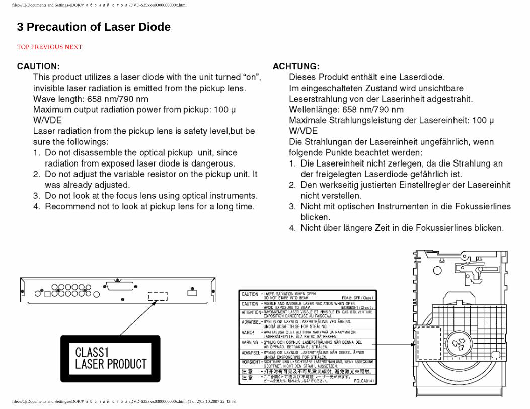
3 Precaution of Laser Diode
TOP PREVIOUS NEXT
file:///C|/Documents and Settings/eDOK/Рабочий стол/DVD-S35xx/s0300000000x.html (1 of 2)03.10.2007 22:43:53
file:///C|/Documents and Settings/eDOK/Рабочий стол/DVD-S35xx/s0300000000x.html
TOP PREVIOUS NEXT
file:///C|/Documents and Settings/eDOK/Рабочий стол/DVD-S35xx/s0300000000x.html (2 of 2)03.10.2007 22:43:53
file:///C|/Documents and Settings/eDOK/Рабочий стол/DVD-S35xx/s0400000000x.html
4 About lead free solder (PbF)
TOP PREVIOUS NEXT
Caution:
Pb free solder has a higher melting point than standard solder; Typically thmelting point is 50 - 70°F (30 - 40°C) higher. Please use a high temperature soldering iron. In case of the soldering iron with temperature control,pleaseset it to 700 ± 20°F (370 ± 10°C).
Pb free solder will tend to splash when heated too high (about 1100°F/ 600°C).
When soldering or unsoldering, please completely remove all of the solder on the pins or solder area, and be sure to heat the soldering points with the Pb free solder until it melts enough.
TOP PREVIOUS NEXT
file:///C|/Documents and Settings/eDOK/Рабочий стол/DVD-S35xx/s0400000000x.html03.10.2007 22:43:57
file:///C|/Documents and Settings/eDOK/Рабочий стол/DVD-S35xx/s0500000000o.html
5 General Description
TOP PREVIOUS NEXT
5.1 Operating instructions
TOP PREVIOUS NEXT
file:///C|/Documents and Settings/eDOK/Рабочий стол/DVD-S35xx/s0500000000o.html03.10.2007 22:44:01
file:///C|/Documents and Settings/eDOK/Рабочий стол/DVD-S35xx/s0501000000.html
5.1 Operating instructions
TOP PREVIOUS NEXT
TOP PREVIOUS NEXT
file:///C|/Documents and Settings/eDOK/Рабочий стол/DVD-S35xx/s0501000000.html03.10.2007 22:44:05
file:///C|/Documents and Settings/eDOK/Рабочий стол/DVD-S35xx/s0600000000x.html
6 PREVENTION OF STATIC ELECTRICITY DISCHARGE
TOP PREVIOUS NEXT
The laser diode in the traverse unit (optical pickup) may brake down due to static electricity of clothes or human body. Use due caution to electrostatic breakdown when servicing and handling the laser diode.
6.1 Grounding for electrostatic breakdown prevention
6.1.1 Worktable grounding
6.1.2 Human body grounding
6.1.3 Handling of optical pickup
6.2 Handling Precautions for Traverse Unit (Optical Pickup)
TOP PREVIOUS NEXT
file:///C|/Documents and Settings/eDOK/Рабочий стол/DVD-S35xx/s0600000000x.html03.10.2007 22:44:28
file:///C|/Documents and Settings/eDOK/Рабочий стол/DVD-S35xx/s0601000000.html
6.1 Grounding for electrostatic breakdown prevention
TOP PREVIOUS NEXT
Some devices such as the DVD player use the optical pickup (laser diode) and the optical pickup will be damaged by static electricity in the working environment. Proceed servicing works under the working environment where grounding works is completed.
6.1.1 Worktable grounding
6.1.2 Human body grounding
6.1.3 Handling of optical pickup
TOP PREVIOUS NEXT
file:///C|/Documents and Settings/eDOK/Рабочий стол/DVD-S35xx/s0601000000.html03.10.2007 22:44:32
file:///C|/Documents and Settings/eDOK/Рабочий стол/DVD-S35xx/s0601010000.html
6.1.1 Worktable grounding
TOP PREVIOUS NEXT
1. Put a conductive material (sheet) or iron sheet on the area where the optical pickup is placed, and ground the sheet.
TOP PREVIOUS NEXT
file:///C|/Documents and Settings/eDOK/Рабочий стол/DVD-S35xx/s0601010000.html03.10.2007 22:44:37
file:///C|/Documents and Settings/eDOK/Рабочий стол/DVD-S35xx/s0601020000.html
6.1.2 Human body grounding
TOP PREVIOUS NEXT
1. Use the anti-static wrist strap to discharge the static electricity form your body.
TOP PREVIOUS NEXT
file:///C|/Documents and Settings/eDOK/Рабочий стол/DVD-S35xx/s0601020000.html03.10.2007 22:44:40
/DVD-S35xx/s0601030000.htmlстол Рабочийfile:///C|/Documents and Settings/eDOK/
6.1.3 Handling of optical pickup
TOP PREVIOUS NEXT
1. To keep the good quality of the optical pickup maintenance parts during transportation and before installation, the both ends of the laser diode are short-circuited. After replacing the parts with new ones, remove the short circuit accordingtothe correct procedure. (See this Technical Guide.)
2. Do not use a tester to check the laser diode for the optical pickup. Failure to do so will damage the laser diode due to the power supply in the tester.
TOP PREVIOUS NEXT
/DVD-S35xx/s0601030000.html03.10.2007 22:44:44стол Рабочийfile:///C|/Documents and Settings/eDOK/
file:///C|/Documents and Settings/eDOK/Рабочий стол/DVD-S35xx/s0602000000.html
6.2 Handling Precautions for Traverse Unit (Optical Pickup)
TOP PREVIOUS NEXT
1. Do not give a considerable shock to the traverse unit (optical pickup) as it has an extremely high-precise structure.
2. When replacing the optical pickup, install the flexible cable and cut its short land with a nipper. See the optical pickup replacement procedure in this Technical Guide. Before replacing the traverse unit, remove the short pin for preventingstaticelectricity and install a new unit. Connect the connector as short times as possible.
3. The flexible cable may be cut off if an excessive force is applied to it. Use caution when handling the cable.
4. The half-fixed resistor for laser power adjustment cannot be adjusted. Do not turn the resistor.
TOP PREVIOUS NEXT
file:///C|/Documents and Settings/eDOK/Рабочий стол/DVD-S35xx/s0602000000.html03.10.2007 22:44:49
file:///C|/Documents and Settings/eDOK/Рабочий стол/DVD-S35xx/s0700000000x.html
7 Disassembling the Casing and Checking P.C.B.s
TOP PREVIOUS NEXT
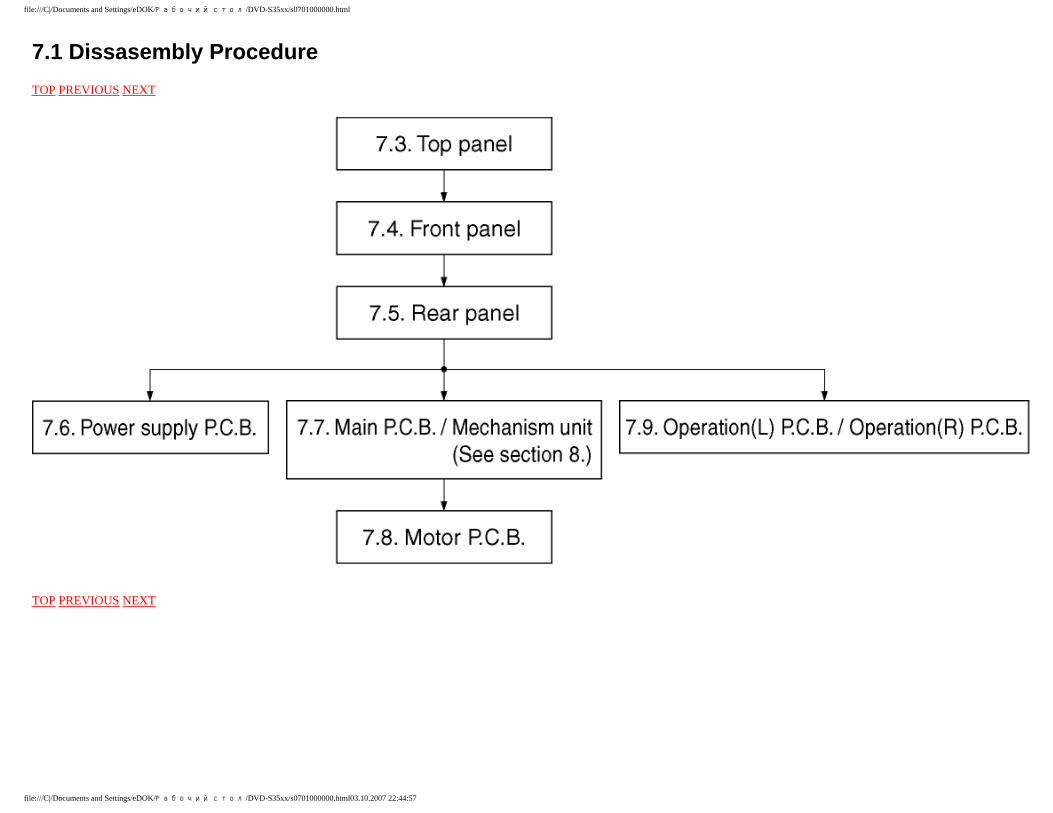
7.1 Dissasembly Procedure
7.2 Casing Parts and P.C.B. Positions
7.3 Top Panel
7.4 Front Panel
7.5 Rear panel
7.6 Power supply P.C.B.
7.7 Main P.C.B. and Mechanism Unit
7.8 Motor P.C.B.
7.9 Operation (L) P.C.B. and Operation (R) P.C.B.
7.10 Service Position
7.10.1 Servicing position of the Main P.C.B. and the Operation P.C.B.
7.10.2 List of the Extension Cables
TOP PREVIOUS NEXT
file:///C|/Documents and Settings/eDOK/Рабочий стол/DVD-S35xx/s0700000000x.html03.10.2007 22:44:53
file:///C|/Documents and Settings/eDOK/Рабочий стол/DVD-S35xx/s0701000000.html
7.1 Dissasembly Procedure
TOP PREVIOUS NEXT
TOP PREVIOUS NEXT
file:///C|/Documents and Settings/eDOK/Рабочий стол/DVD-S35xx/s0701000000.html03.10.2007 22:44:57
file:///C|/Documents and Settings/eDOK/Рабочий стол/DVD-S35xx/s0702000000.html
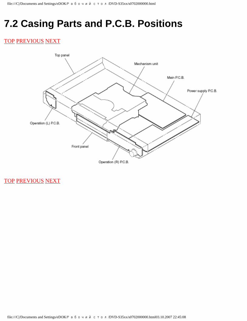
7.2 Casing Parts and P.C.B. Positions
TOP PREVIOUS NEXT
TOP PREVIOUS NEXT
file:///C|/Documents and Settings/eDOK/Рабочий стол/DVD-S35xx/s0702000000.html03.10.2007 22:45:08
file:///C|/Documents and Settings/eDOK/Рабочий стол/DVD-S35xx/s0703000000.html
7.3 Top Panel
TOP PREVIOUS NEXT
1. Unscrew the screws.
TOP PREVIOUS NEXT
file:///C|/Documents and Settings/eDOK/Рабочий стол/DVD-S35xx/s0703000000.html03.10.2007 22:45:12
file:///C|/Documents and Settings/eDOK/Рабочий стол/DVD-S35xx/s0704000000.html
7.4 Front Panel
TOP PREVIOUS NEXT
1. Pull the tray out of the mechanism unit. Remove the gear and install it onto a screwdriver to make a gear jig.
2. Insert the gear jig into the tray open/ close hole.
3. Turn the gear jig counterclockwise to open the tray.
4. Remove the tray top from the tray section.
file:///C|/Documents and Settings/eDOK/Рабочий стол/DVD-S35xx/s0704000000.html (1 of 3)03.10.2007 22:45:16
file:///C|/Documents and Settings/eDOK/Рабочий стол/DVD-S35xx/s0704000000.html
5. Unscrew the screws.
6. Remove the connector.
7. Release the tabs.
8. Remove the connector.
file:///C|/Documents and Settings/eDOK/Рабочий стол/DVD-S35xx/s0704000000.html (2 of 3)03.10.2007 22:45:16
file:///C|/Documents and Settings/eDOK/Рабочий стол/DVD-S35xx/s0704000000.html
TOP PREVIOUS NEXT
file:///C|/Documents and Settings/eDOK/Рабочий стол/DVD-S35xx/s0704000000.html (3 of 3)03.10.2007 22:45:16
/DVD-S35xx/s0705000000.htmlстол Рабочийfile:///C|/Documents and Settings/eDOK/
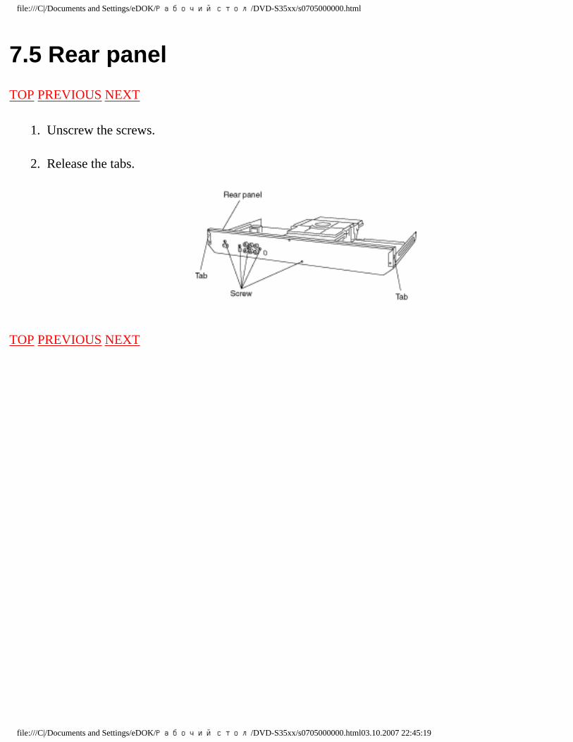
7.5 Rear panel
TOP PREVIOUS NEXT
1. Unscrew the screws.
2. Release the tabs.
TOP PREVIOUS NEXT
/DVD-S35xx/s0705000000.html03.10.2007 22:45:19стол Рабочийfile:///C|/Documents and Settings/eDOK/
file:///C|/Documents and Settings/eDOK/Рабочий стол/DVD-S35xx/s0706000000.html
7.6 Power supply P.C.B.
TOP PREVIOUS NEXT
1. Unscrew the screws.
2. Remove the connector.
file:///C|/Documents and Settings/eDOK/Рабочий стол/DVD-S35xx/s0706000000.html (1 of 2)03.10.2007 22:45:26
file:///C|/Documents and Settings/eDOK/Рабочий стол/DVD-S35xx/s0706000000.html
TOP PREVIOUS NEXT
file:///C|/Documents and Settings/eDOK/Рабочий стол/DVD-S35xx/s0706000000.html (2 of 2)03.10.2007 22:45:26
file:///C|/Documents and Settings/eDOK/Рабочий стол/DVD-S35xx/s0707000000.html
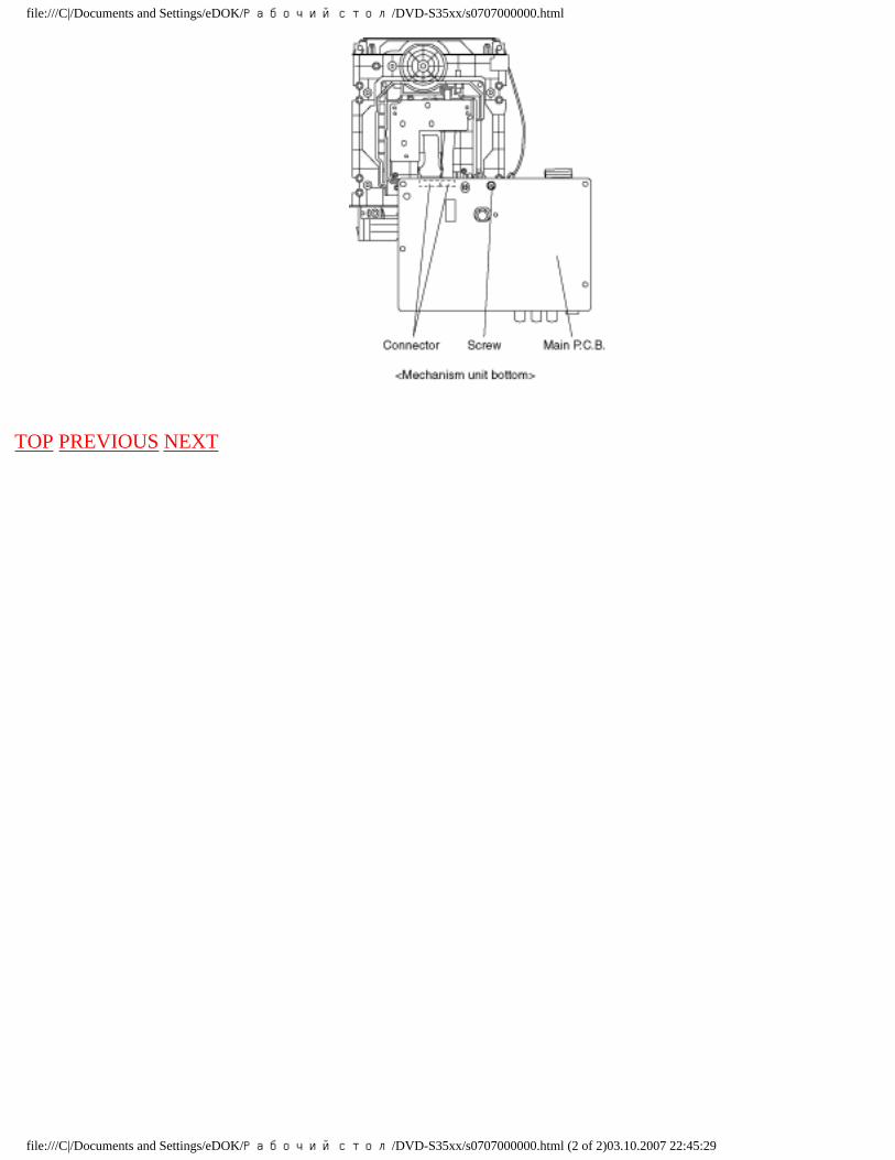
7.7 Main P.C.B. and Mechanism Unit
TOP PREVIOUS NEXT
1. Unscrew the screws.
2. Remove the connectors.
3. Pull out the Main P.C.B. and mechanism unit vertically.
4. Unscrew the screw.
5. Remove the connectors.
file:///C|/Documents and Settings/eDOK/Рабочий стол/DVD-S35xx/s0707000000.html (1 of 2)03.10.2007 22:45:29
file:///C|/Documents and Settings/eDOK/Рабочий стол/DVD-S35xx/s0707000000.html
TOP PREVIOUS NEXT
file:///C|/Documents and Settings/eDOK/Рабочий стол/DVD-S35xx/s0707000000.html (2 of 2)03.10.2007 22:45:29
/DVD-S35xx/s0708000000.htmlстол Рабочийfile:///C|/Documents and Settings/eDOK/
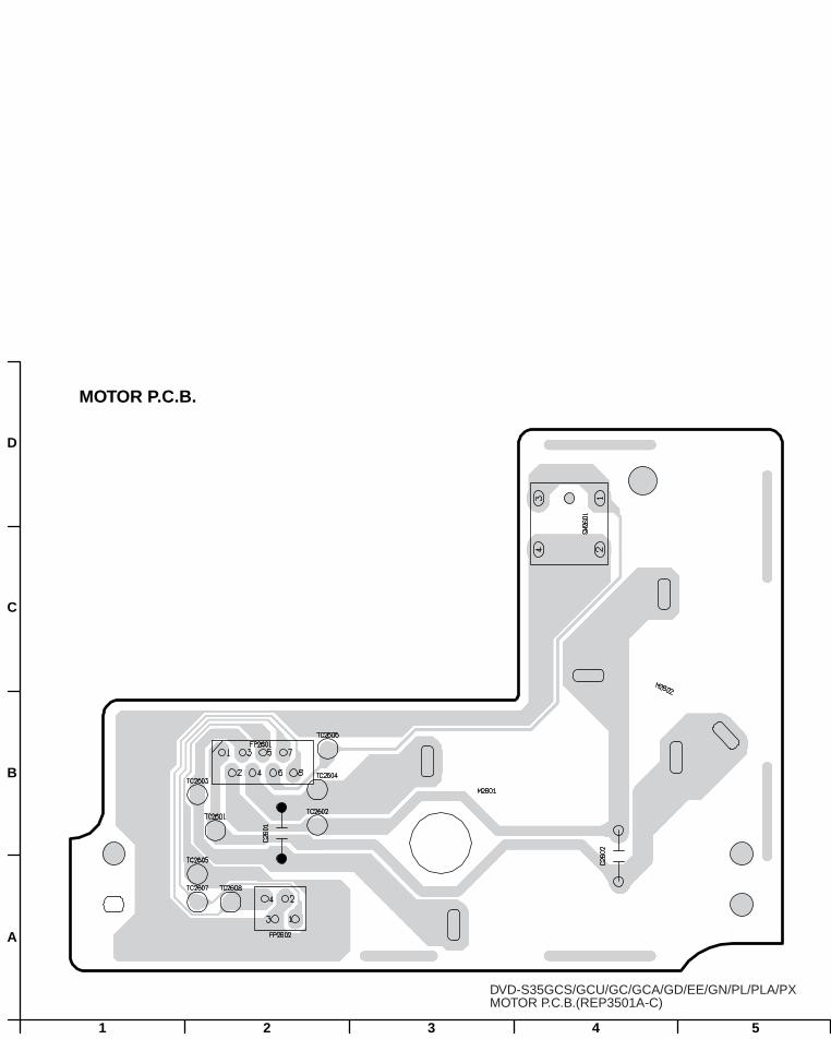
7.8 Motor P.C.B.
TOP PREVIOUS NEXT
1. Unscrew the screw.
2. Remove the solders.
3. Remove the connector.
TOP PREVIOUS NEXT
/DVD-S35xx/s0708000000.html03.10.2007 22:45:33стол Рабочийfile:///C|/Documents and Settings/eDOK/
file:///C|/Documents and Settings/eDOK/Рабочий стол/DVD-S35xx/s0709000000.html
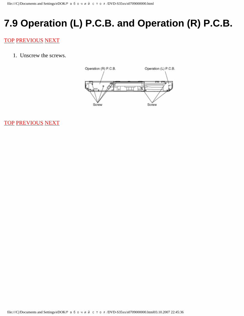
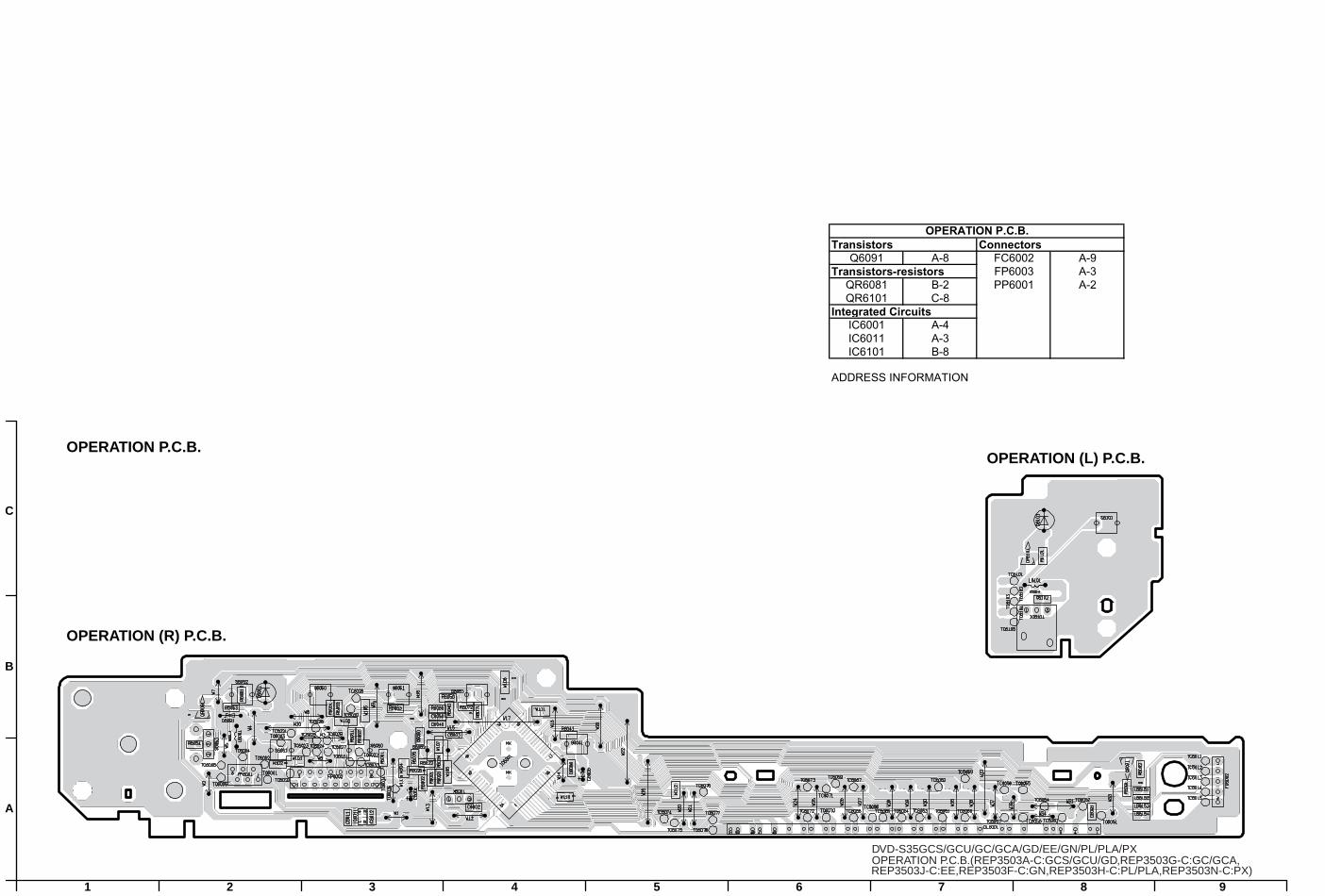
7.9 Operation (L) P.C.B. and Operation (R) P.C.B.
TOP PREVIOUS NEXT
1. Unscrew the screws.
TOP PREVIOUS NEXT
file:///C|/Documents and Settings/eDOK/Рабочий стол/DVD-S35xx/s0709000000.html03.10.2007 22:45:36
file:///C|/Documents and Settings/eDOK/Рабочий стол/DVD-S35xx/s0710000000.html
7.10 Service Position
TOP PREVIOUS NEXT
7.10.1 Servicing position of the Main P.C.B. and the Operation P.C.B.
7.10.2 List of the Extension Cables
TOP PREVIOUS NEXT
file:///C|/Documents and Settings/eDOK/Рабочий стол/DVD-S35xx/s0710000000.html03.10.2007 22:45:40
file:///C|/Documents and Settings/eDOK/Рабочий стол/DVD-S35xx/s0710010000.html
7.10.1 Servicing position of the Main P.C.B. and the Operation P.C.B.
TOP PREVIOUS NEXT
TOP PREVIOUS NEXT
file:///C|/Documents and Settings/eDOK/Рабочий стол/DVD-S35xx/s0710010000.html03.10.2007 22:45:45
file:///C|/Documents and Settings/eDOK/Рабочий стол/DVD-S35xx/s0710020000.html
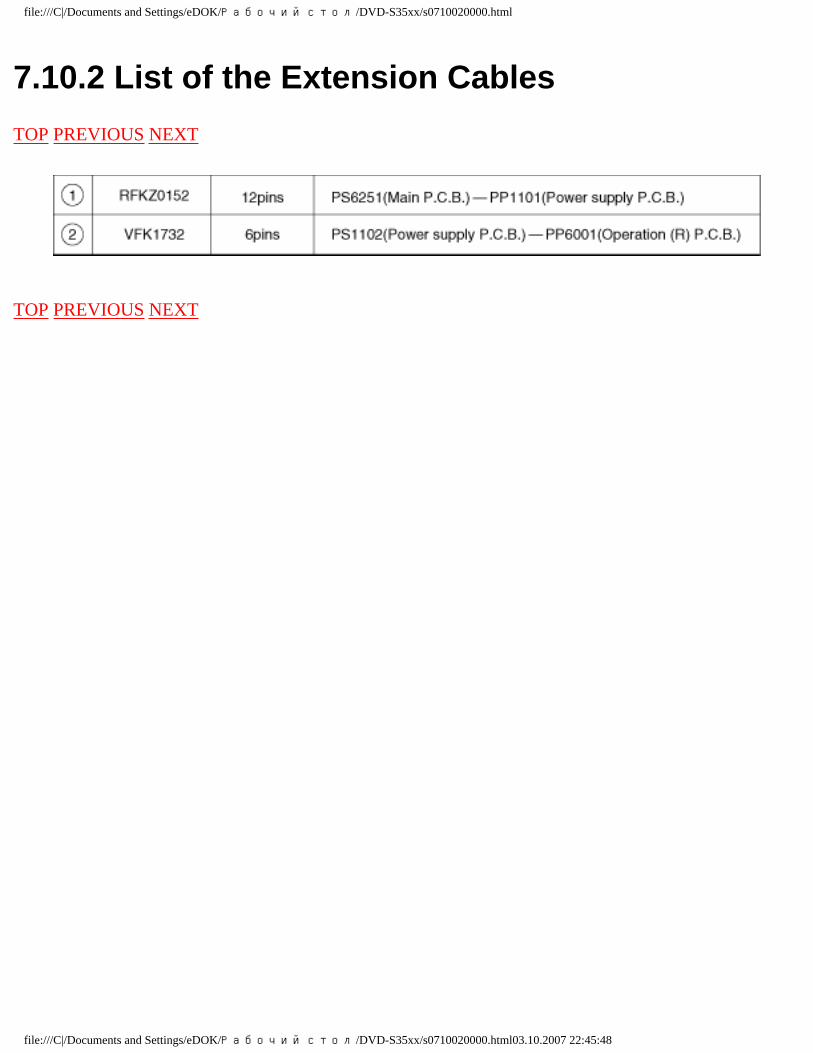
7.10.2 List of the Extension Cables
TOP PREVIOUS NEXT
TOP PREVIOUS NEXT
file:///C|/Documents and Settings/eDOK/Рабочий стол/DVD-S35xx/s0710020000.html03.10.2007 22:45:48
file:///C|/Documents and Settings/eDOK/Рабочий стол/DVD-S35xx/s0800000000x.html
8 ASSEMBLING AND DISASSEMBLING THE MECHANISM UNIT
TOP PREVIOUS NEXT
8.1 Disassembly Procedure
8.2 Motor P.C.B.
8.3 Clamp Plate Unit
8.4 Tray
8.5 Traverse Block
8.6 Traverse Gear
8.7 Optical Pickup Unit
8.7.1 Precautions in optical pickup replacement
8.7.2 Disassembling the Optical Pickup Unit
8.7.3 Cautions to Be Taken When Replacing the Optical Pickup
8.8 Disassembling the Middle Chassis
8.9 Disassembling the Traverse Gear A/ FG P.C.B.
8.10 Disassembling the Spindle Motor Unit
TOP PREVIOUS NEXT
file:///C|/Documents and Settings/eDOK/Рабочий стол/DVD-S35xx/s0800000000x.html03.10.2007 22:45:54
/DVD-S35xx/s0801000000.htmlстол Рабочийfile:///C|/Documents and Settings/eDOK/
8.1 Disassembly Procedure
TOP PREVIOUS NEXT
TOP PREVIOUS NEXT
/DVD-S35xx/s0801000000.html03.10.2007 22:45:59стол Рабочийfile:///C|/Documents and Settings/eDOK/
file:///C|/Documents and Settings/eDOK/Рабочий стол/DVD-S35xx/s0802000000.html
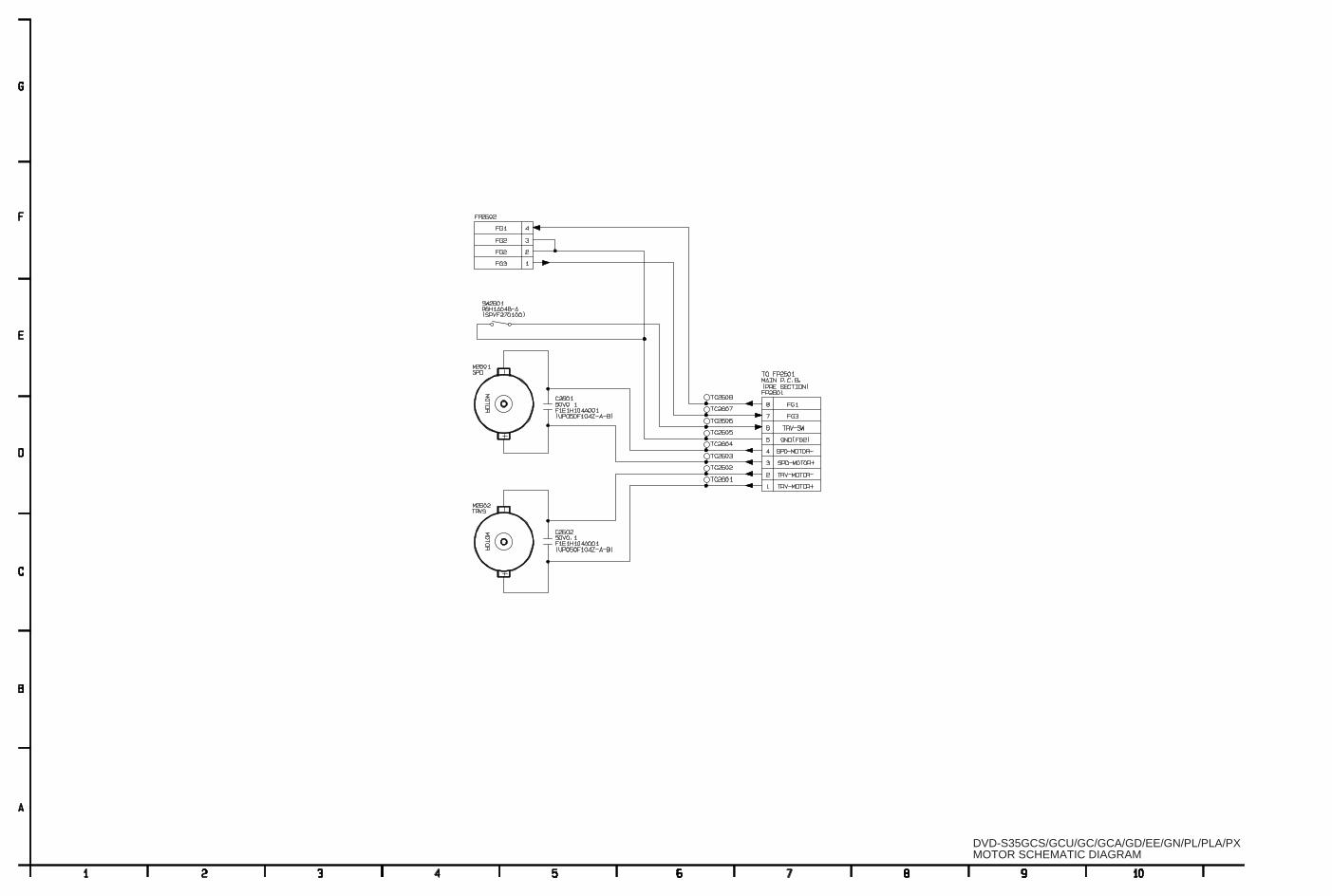
8.2 Motor P.C.B.
TOP PREVIOUS NEXT
1. Unscrew the screw.
2. Remove the solders.
3. Remove the connector.
TOP PREVIOUS NEXT
file:///C|/Documents and Settings/eDOK/Рабочий стол/DVD-S35xx/s0802000000.html03.10.2007 22:46:04
file:///C|/Documents and Settings/eDOK/Рабочий стол/DVD-S35xx/s0803000000.html
8.3 Clamp Plate Unit
TOP PREVIOUS NEXT
1. Spread the stopper with hand to slide the tabs and remove the clamp plate unit.
TOP PREVIOUS NEXT
file:///C|/Documents and Settings/eDOK/Рабочий стол/DVD-S35xx/s0803000000.html03.10.2007 22:46:08
file:///C|/Documents and Settings/eDOK/Рабочий стол/DVD-S35xx/s0804000000.html
8.4 Tray
TOP PREVIOUS NEXT
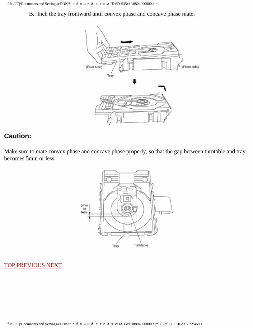
1. Lift the tray.
<Precautions in reassembling the tray>
•Reassemble the tray so that it is in the backmost position.
1. Turn traverse gear until cam gear leaver comes to the lever adjusting position at the end of mechanical chassis unit.
file:///C|/Documents and Settings/eDOK/Рабочий стол/DVD-S35xx/s0804000000.html (1 of 3)03.10.2007 22:46:11
file:///C|/Documents and Settings/eDOK/Рабочий стол/DVD-S35xx/s0804000000.html
2. Check the position of convex phase on back of the tray, and that of concave phase on drive gear.
A. Place the tray on the unit from rearward.
file:///C|/Documents and Settings/eDOK/Рабочий стол/DVD-S35xx/s0804000000.html (2 of 3)03.10.2007 22:46:11
file:///C|/Documents and Settings/eDOK/Рабочий стол/DVD-S35xx/s0804000000.html
B. Inch the tray frontward until convex phase and concave phase mate.
Caution:
Make sure to mate convex phase and concave phase properly, so that the gap between turntable and tray becomes 5mm or less.
TOP PREVIOUS NEXT
file:///C|/Documents and Settings/eDOK/Рабочий стол/DVD-S35xx/s0804000000.html (3 of 3)03.10.2007 22:46:11
file:///C|/Documents and Settings/eDOK/Рабочий стол/DVD-S35xx/s0805000000.html
8.5 Traverse Block
TOP PREVIOUS NEXT
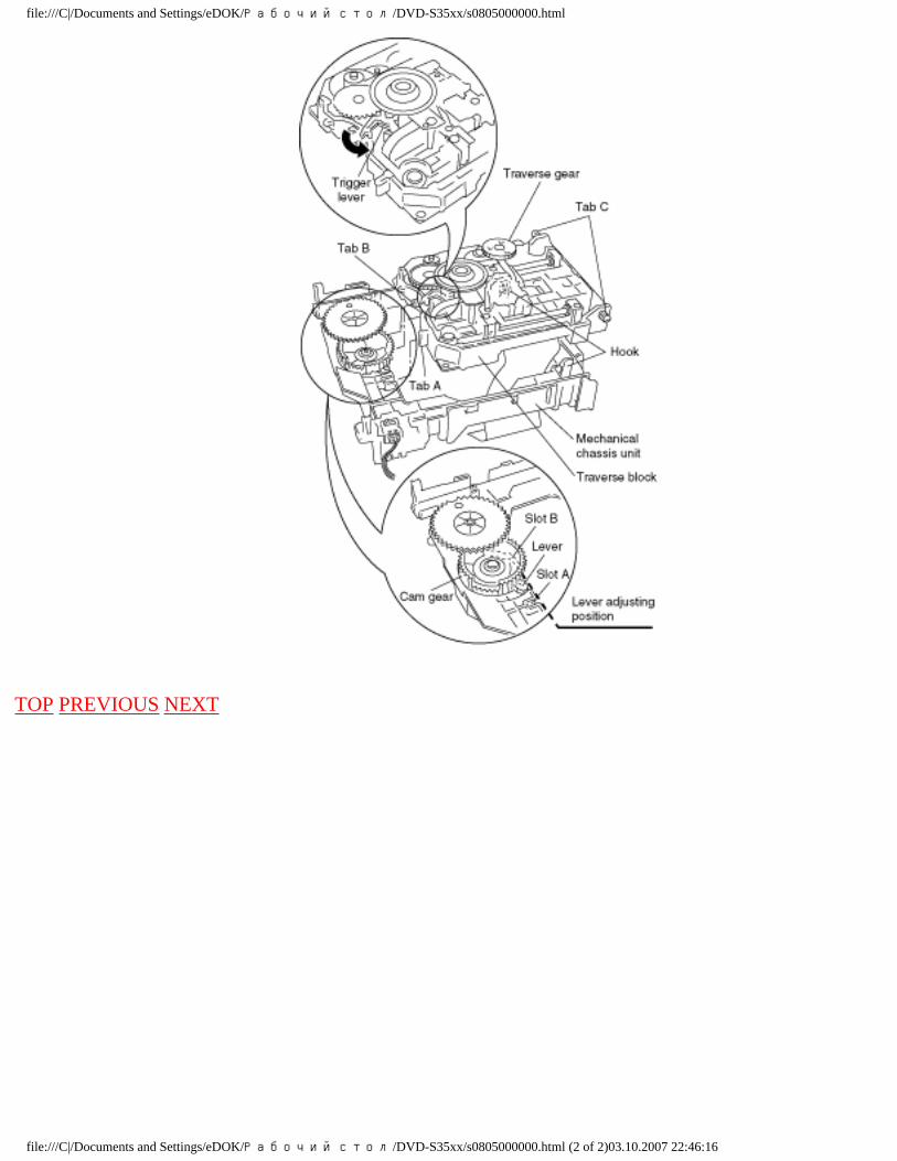
1. Lift the traverse block while spreading the hook of the mechanical chassis unit.
2. Disengage the tabs from the holes of the mechanical chassis unit.
<Precautions in reassembling the traverse block>
•Take the following precautions when reassembling the traverse block.
1. Turn traverse gear on the traverse block to let trigger lever turn rightward. (Front view)
2. Bring cam gear lever to the lever adjusting position at the end of mechanical chassis unit.
3. Put tabs A and B into slots A and B respectively.
Place tabs C into hooks to mount the traverse block on mechanical chassis unit. (Slot A... Mechanical chassis unit, Slot B... Cam gear)
file:///C|/Documents and Settings/eDOK/Рабочий стол/DVD-S35xx/s0805000000.html (1 of 2)03.10.2007 22:46:16
file:///C|/Documents and Settings/eDOK/Рабочий стол/DVD-S35xx/s0805000000.html
TOP PREVIOUS NEXT
file:///C|/Documents and Settings/eDOK/Рабочий стол/DVD-S35xx/s0805000000.html (2 of 2)03.10.2007 22:46:16
file:///C|/Documents and Settings/eDOK/Рабочий стол/DVD-S35xx/s0806000000.html
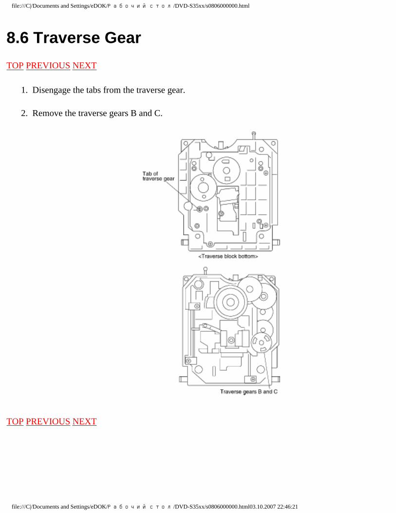
8.6 Traverse Gear
TOP PREVIOUS NEXT
1. Disengage the tabs from the traverse gear.
2. Remove the traverse gears B and C.
TOP PREVIOUS NEXT
file:///C|/Documents and Settings/eDOK/Рабочий стол/DVD-S35xx/s0806000000.html03.10.2007 22:46:21
/DVD-S35xx/s0807000000.htmlстол Рабочийfile:///C|/Documents and Settings/eDOK/
8.7 Optical Pickup Unit
TOP PREVIOUS NEXT
1. Make the right turn the trigger lever.
2. Unscrew the screws.
3. Remove the spring holders and the springs.
4. Pull out the drive shaft and guide shaft.
8.7.1 Precautions in optical pickup replacement
8.7.2 Disassembling the Optical Pickup Unit
8.7.3 Cautions to Be Taken When Replacing the Optical Pickup
TOP PREVIOUS NEXT
/DVD-S35xx/s0807000000.html03.10.2007 22:46:25стол Рабочийfile:///C|/Documents and Settings/eDOK/
file:///C|/Documents and Settings/eDOK/Рабочий стол/DVD-S35xx/s0807010000.html
8.7.1 Precautions in optical pickup replacement
TOP PREVIOUS NEXT
The optical pickup can be damaged by static electricity from you body. Be sure to take static electricity countermeasures when working around the optical pickup. (Refer to the related page in this Manual about the countermeasures.)
1. Do not touch laser diode, actuator and their peripheries.
2. Do not use tester to check laser diode. (Laser diode can be damaged easily.)
3. The use of soldering iron with anti-static feature is recommended when providing short-circuit to laser diode or when removing it.
4. Solder the land on flexible cable of optical pickup unit.
Caution
When using the soldering iron without anti-static feature, short-circuit the flexible cable terminal with a clip before short-circuiting the land.
After intended repair is finished, remove the solder for short-circuit of laser diode in a correct way following the procedures described in this Manual.
TOP PREVIOUS NEXT
file:///C|/Documents and Settings/eDOK/Рабочий стол/DVD-S35xx/s0807010000.html03.10.2007 22:46:28
file:///C|/Documents and Settings/eDOK/Рабочий стол/DVD-S35xx/s0807020000.html
8.7.2 Disassembling the Optical Pickup Unit
TOP PREVIOUS NEXT
1. Remove the 2 screws A and remove the TRV feed rack.
2. Remove the screw B and remove the Terminal FPC.
3. Remove the optical pickup.
Fig. 1
TOP PREVIOUS NEXT
file:///C|/Documents and Settings/eDOK/Рабочий стол/DVD-S35xx/s0807020000.html03.10.2007 22:46:33
file:///C|/Documents and Settings/eDOK/Рабочий стол/DVD-S35xx/s0807030000.html
8.7.3 Cautions to Be Taken When Replacing the Optical Pickup
TOP PREVIOUS NEXT
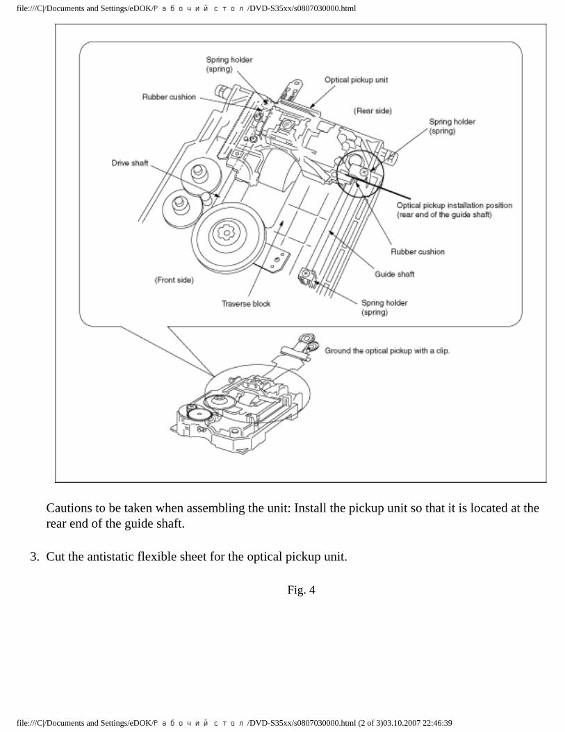
An antistatic flexible sheet (FPC) is connected with the new optical pickup.
Replace the optical pickup according to the following procedure.
1. Install the Terminal FPC, TRV feed rack on the optical pickup. (See Fig. 1 )
Fig. 2
2. Install the optical pickup unit, spring, drive shaft, guide shaft, rubber cushion, and spring holder on the traverse block.
Fig. 3
file:///C|/Documents and Settings/eDOK/Рабочий стол/DVD-S35xx/s0807030000.html (1 of 3)03.10.2007 22:46:39
file:///C|/Documents and Settings/eDOK/Рабочий стол/DVD-S35xx/s0807030000.html
Cautions to be taken when assembling the unit: Install the pickup unit so that it is located at the rear end of the guide shaft.
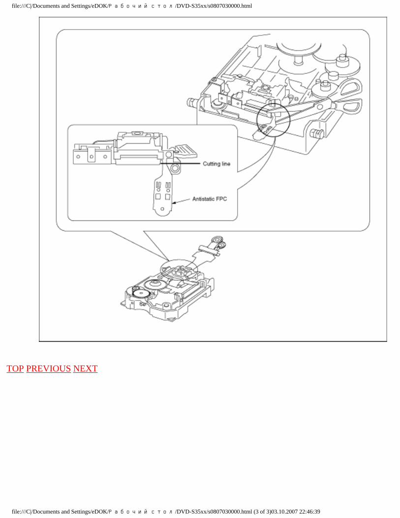
3. Cut the antistatic flexible sheet for the optical pickup unit.
Fig. 4
file:///C|/Documents and Settings/eDOK/Рабочий стол/DVD-S35xx/s0807030000.html (2 of 3)03.10.2007 22:46:39
file:///C|/Documents and Settings/eDOK/Рабочий стол/DVD-S35xx/s0807030000.html
TOP PREVIOUS NEXT
file:///C|/Documents and Settings/eDOK/Рабочий стол/DVD-S35xx/s0807030000.html (3 of 3)03.10.2007 22:46:39
file:///C|/Documents and Settings/eDOK/Рабочий стол/DVD-S35xx/s0808000000.html
8.8 Disassembling the Middle Chassis
TOP PREVIOUS NEXT
1. Remove the holder pins.
2. Remove the tabs.
3. It lifts while pulling it in the direction of the arrow.
TOP PREVIOUS NEXT
file:///C|/Documents and Settings/eDOK/Рабочий стол/DVD-S35xx/s0808000000.html03.10.2007 22:46:43
file:///C|/Documents and Settings/eDOK/Рабочий стол/DVD-S35xx/s0809000000.html
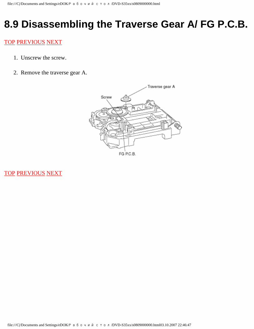
8.9 Disassembling the Traverse Gear A/ FG P.C.B.
TOP PREVIOUS NEXT
1. Unscrew the screw.
2. Remove the traverse gear A.
TOP PREVIOUS NEXT
file:///C|/Documents and Settings/eDOK/Рабочий стол/DVD-S35xx/s0809000000.html03.10.2007 22:46:47
file:///C|/Documents and Settings/eDOK/Рабочий стол/DVD-S35xx/s0810000000.html
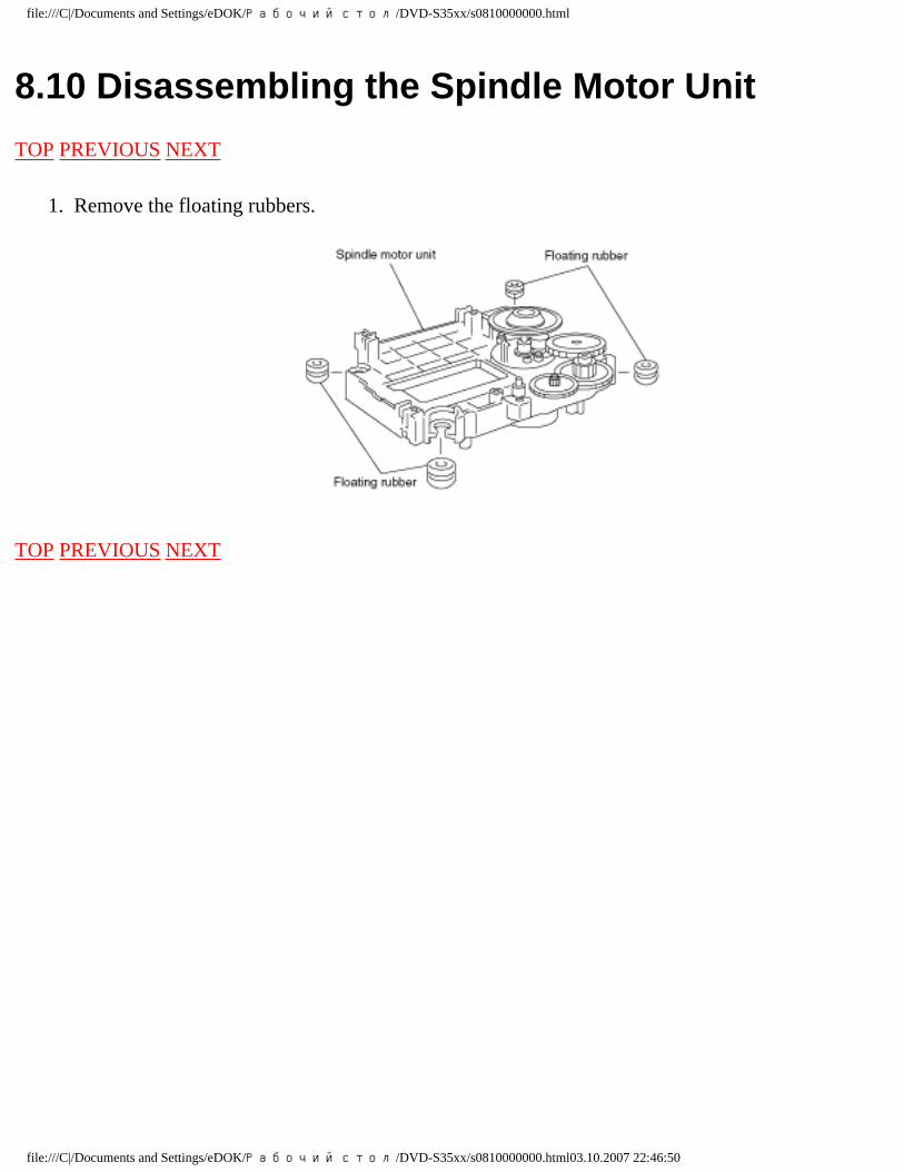
8.10 Disassembling the Spindle Motor Unit
TOP PREVIOUS NEXT
1. Remove the floating rubbers.
TOP PREVIOUS NEXT
file:///C|/Documents and Settings/eDOK/Рабочий стол/DVD-S35xx/s0810000000.html03.10.2007 22:46:50
file:///C|/Documents and Settings/eDOK/Рабочий стол/DVD-S35xx/s0900000000x.html
9 Self-Diagnosis Function and Service Modes
TOP PREVIOUS NEXT
9.1 Optical Pickup Breakdown Diagnosis
9.2 Service Mode Table 1
9.3 DVD Self Diagnostic Function-Error Code
9.4 Last Error Code saved during NO PLAY
9.5 Service mode table 2
9.6 Sales demonstration lock function
9.6.1 Setting
9.6.2 Cancellation
9.7 Handling After Completing Repairs
9.7.1 Method
9.7.2 Precautions
TOP PREVIOUS NEXT
file:///C|/Documents and Settings/eDOK/Рабочий стол/DVD-S35xx/s0900000000x.html03.10.2007 22:47:03
file:///C|/Documents and Settings/eDOK/Рабочий стол/DVD-S35xx/s0901000000.html
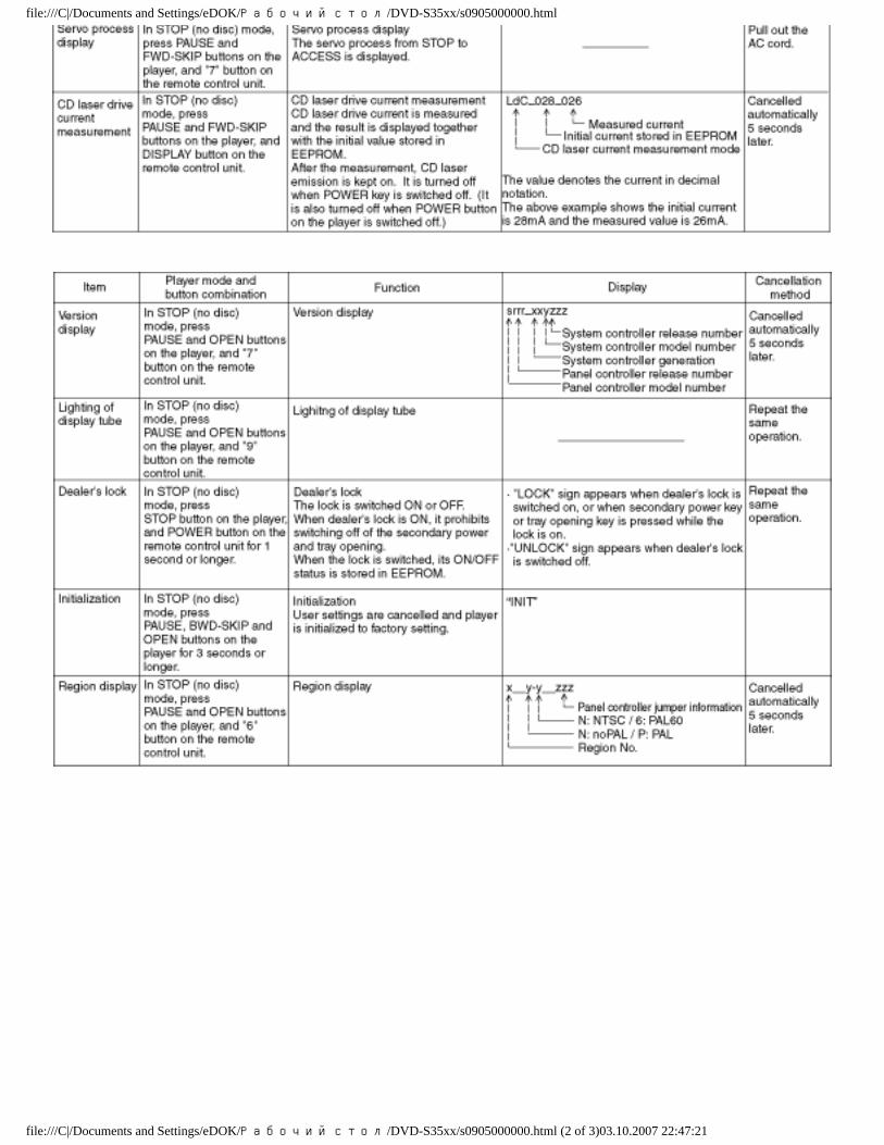
9.1 Optical Pickup Breakdown Diagnosis
TOP PREVIOUS NEXT
The optical pickup self-diagnosis function and tilt adjustment check function have been included in this unit. When repairing, use the following procedure for effective Self-diagnosis and tilt adjustment.Be sure to use the self-diagnosis functionbeforereplacing the optical pickup when "NO DISC" is displayed. As a guideline, you should replace the optical pickup when the value of the laser drive current is more than 55.
Note:
Press the power button to turn on the power, and check the value within three minutes before the unit warms up. (Otherwise, the result will be incorrect.)
file:///C|/Documents and Settings/eDOK/Рабочий стол/DVD-S35xx/s0901000000.html (1 of 2)03.10.2007 22:47:06
file:///C|/Documents and Settings/eDOK/Рабочий стол/DVD-S35xx/s0901000000.html
TOP PREVIOUS NEXT
file:///C|/Documents and Settings/eDOK/Рабочий стол/DVD-S35xx/s0901000000.html (2 of 2)03.10.2007 22:47:06
file:///C|/Documents and Settings/eDOK/Рабочий стол/DVD-S35xx/s0902000000.html
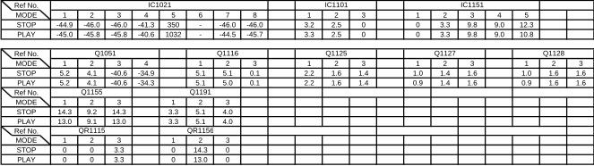
9.2 Service Mode Table 1
TOP PREVIOUS NEXT
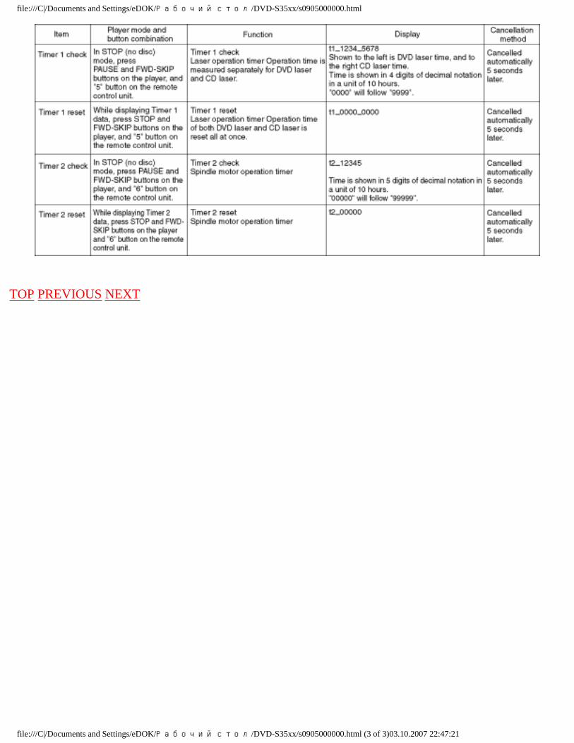
The service modes can be activated by pressing various button combination on the player and remote control unit.
Player buttons Remote control unit buttons Application Note
PAUSE +
OPEN/CLOSE
0 Displaying the UHF display F_ _ _ Refer to section 9.3. Self-Diagnosis Function (UHF Display).
5 Jitter check, tilt adjustment *Display shows J_xxx_yyy_zz "yyy" and "zz" shown to the right have nothing to do with the jitter value. "yyy" is the error counter, while "zz" is the focusdrive value. Referto section 11.4. for Optical Pickup Tilt Adjustment Procedure.
Refer to section 11.4. Optical Pickup Tilt Adjustment
6 Checking the region numbers and broadcast system
7 Checking the program version Check the IC6301 FLASH ROM program.
9 Lighting Confirmation Function of Display Tube
DISPLAY Checking the laser drive current Refer to section 8 Optical Pickup Replacement Procedure.
PAUSE Writing the laser drive current value after replacing the optical pickup (do not use for anything other than optical pickup replacement)
PAUSE SKIP/
SEARCH<< OPEN/CLOSE
Initializing the DVD player (restoring factory preset settings)
Refer to section 9.5. Initializing the DVD player.
TOP PREVIOUS NEXT
file:///C|/Documents and Settings/eDOK/Рабочий стол/DVD-S35xx/s0902000000.html03.10.2007 22:47:09
file:///C|/Documents and Settings/eDOK/Рабочий стол/DVD-S35xx/s0903000000.html
H06 Power error Cannot switch off the power because of the panel and system computer communication error
H07 Spindle motor drive error
Spindle motor ass’y
DSC related
F500 DSC error DV1 (IC3001) stops in the occurence of servo error (starup, focus error, etc)
Optical pickup
DV1 (IC3001)
DV1 (IC3001)
servo drive
F501 DSC not Ready DSC-system computer communication error (Communication failure caused by idling of DSC)
DV1 (IC3001)
DV1 (IC3001)
F502 DSC Time out error Similar disposal as F500 Optical pickup
DV1 (IC3001)
DV1 (IC3001)
servo drive
F503 DSC communication Failure
Communication error (result error occured although communication command was sent)
DV1 (IC3001)
DV1 (IC3001)
EEPROM (IC6351)
F505 DSC Attention error Similar disposal as F500 Optical pickup
DV1 (IC3001)
DV1 (IC3001)
servo drive
file:///C|/Documents and Settings/eDOK/Рабочий стол/DVD-S35xx/s0903000000.html (1 of 3)03.10.2007 22:47:13
file:///C|/Documents and Settings/eDOK/Рабочий стол/DVD-S35xx/s0903000000.html
F506 Invalid media Disc is flipped over, TOC unreadable, incompatible disc
DISC DV1 (IC3001)
DV1 (IC3001)
DV1 (IC3001)
ODC related
F600 Access failure to management information caused by demodulation error
Operation stopped because navigation data is not accessible caused by the demodulation defect
DV1 (IC3001)
DV1 (IC3001)
DV1 (IC3001)
F601 Indeterminate sector ID requested
Operation stopped caused by the request to access abnormal ID data
DV1 (IC3001)
DV1 (IC3001)
DV1 (IC3001)
F602 Access failure to LEAD-IN caused by demodulation error
LEAD IN data unreadable
F603 Access failure to KEYDET caused by demodulation error
Access failure to CSS data of disc
F610 ODC abnormality No permission for command execution
DV1 (IC3001)
F611 6626 QCODE don’t read Error
Access failure to seek address in CD series
DV1 (IC3001)
F612 No CRC OK for a specific time
Access failure to ID data in DVD series
DV1 (IC3001)
F630 No reply to KEY DET enquiry
(for internal use only)
F631 CPPM KEY DET is not available till the FILE terminal
(CPPM file system is unreadable caused by scratches)
DISC CPPM (*1)
F632 CPPM KEY DET is not available
Been revoked or falsified DISC EEPROM (IC6351)
CPPM (*1)
Disc code
F103 Illegal highlight Position
Big possibility of disc specification violation during highlight display
DISC
HIC Error
F4FF Force initialize failure (time out)
EEPROM (IC6351)
DV1 (IC3001)
DV1 (IC3001)
DV1 (IC3001)
Micro computer error
F700 MBX overflow When replying message to disc manager
F701 Message command does not end
Next message is sent before replying to disc manager
file:///C|/Documents and Settings/eDOK/Рабочий стол/DVD-S35xx/s0903000000.html (2 of 3)03.10.2007 22:47:13
file:///C|/Documents and Settings/eDOK/Рабочий стол/DVD-S35xx/s0903000000.html
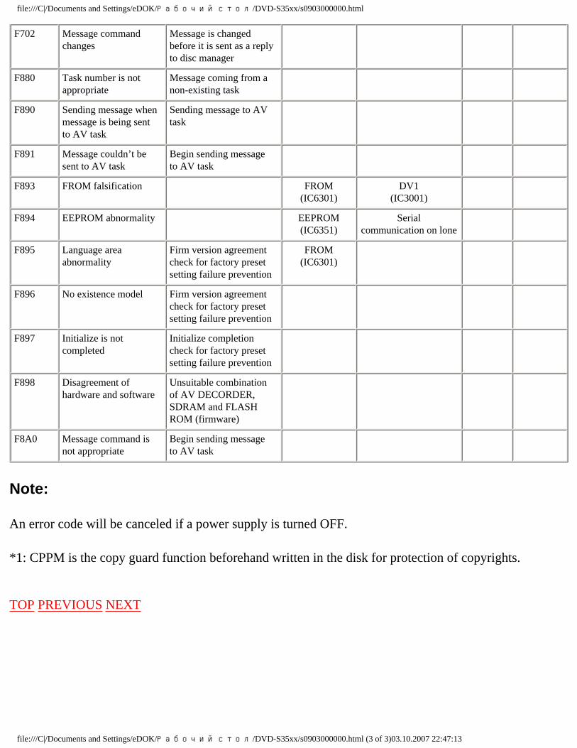
F702 Message command changes
Message is changed before it is sent as a reply to disc manager
F880 Task number is not appropriate
Message coming from a non-existing task
F890 Sending message when message is being sent to AV task
Sending message to AV task
F891 Message couldn’t be sent to AV task
Begin sending message to AV task
F893 FROM falsification FROM (IC6301)
DV1 (IC3001)
F894 EEPROM abnormality EEPROM (IC6351)
Serial communication on lone
F895 Language area abnormality
Firm version agreement check for factory preset setting failure prevention
FROM (IC6301)
F896 No existence model Firm version agreement check for factory preset setting failure prevention
F897 Initialize is not completed
Initialize completion check for factory preset setting failure prevention
F898 Disagreement of hardware and software
Unsuitable combination of AV DECORDER, SDRAM and FLASH ROM (firmware)
F8A0 Message command is not appropriate
Begin sending message to AV task
Note:
An error code will be canceled if a power supply is turned OFF.
*1: CPPM is the copy guard function beforehand written in the disk for protection of copyrights.
TOP PREVIOUS NEXT
file:///C|/Documents and Settings/eDOK/Рабочий стол/DVD-S35xx/s0903000000.html (3 of 3)03.10.2007 22:47:13
file:///C|/Documents and Settings/eDOK/Рабочий стол/DVD-S35xx/s0904000000.html
9.4 Last Error Code saved during NO PLAY
TOP PREVIOUS NEXT
Error code Error Content System computer Setting task System computer internal error code
F0BF 6) Cannot playback because physical layer is not recoginizable
PCND_NOPLAY PHYSICAL 0x50 DriveManager 0xDOBF
F0C0 8) DVD: Cannot playback because it is not DVD Video/Adio/VR
PCND_NOPLAY VIDEO 0x70 DiscManager 0xDOC0
F0C1 9) DVD: Prohibited by the restricted region code
PCND_NOPLAY RCD 0x80 DiscManager 0xDOC1
F0C2 A) DVD: PAL restricted playback PCND_NOPLAY PAL 0x90 DiscManager 0xDOC2
F0C3 B) DVD: Parental lock setting prohibits the playback of the entire title
PCND_NOPLAY PTL 0xA0 DiscManager 0xDOC3
F0C4 C) VCD: Prohibited because it is in PHOTO CD fromat
PCND_NOPLAY PHOTO CD 0xB0 DiscManager 0xDOC4
F0C5 VCD/CD: Prohibited because it is CDROM without CD-DA
PCND_NOPLAY CDROM 0xC0 DiscManager 0xDOC5
TOP PREVIOUS NEXT
file:///C|/Documents and Settings/eDOK/Рабочий стол/DVD-S35xx/s0904000000.html03.10.2007 22:47:17
file:///C|/Documents and Settings/eDOK/Рабочий стол/DVD-S35xx/s0905000000.html
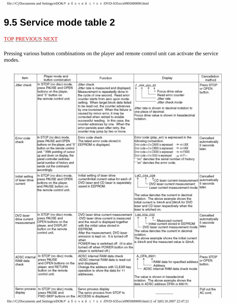
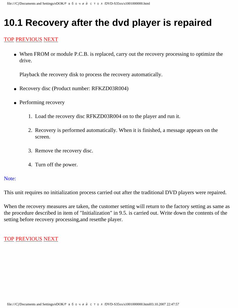
9.5 Service mode table 2
TOP PREVIOUS NEXT
Pressing various button combinations on the player and remote control unit can activate the service modes.
file:///C|/Documents and Settings/eDOK/Рабочий стол/DVD-S35xx/s0905000000.html (1 of 3)03.10.2007 22:47:21
file:///C|/Documents and Settings/eDOK/Рабочий стол/DVD-S35xx/s0905000000.html
file:///C|/Documents and Settings/eDOK/Рабочий стол/DVD-S35xx/s0905000000.html (2 of 3)03.10.2007 22:47:21
file:///C|/Documents and Settings/eDOK/Рабочий стол/DVD-S35xx/s0905000000.html
TOP PREVIOUS NEXT
file:///C|/Documents and Settings/eDOK/Рабочий стол/DVD-S35xx/s0905000000.html (3 of 3)03.10.2007 22:47:21
file:///C|/Documents and Settings/eDOK/Рабочий стол/DVD-S35xx/s0906000000.html
9.6 Sales demonstration lock function
TOP PREVIOUS NEXT
This function prevents discs from being lost when the unit is used for sales demonstrations by disabling the disc eject function. "LOCK" is displayed on the unit, and ordinary operation is disabled.
9.6.1 Setting
9.6.2 Cancellation
TOP PREVIOUS NEXT
file:///C|/Documents and Settings/eDOK/Рабочий стол/DVD-S35xx/s0906000000.html03.10.2007 22:47:24
file:///C|/Documents and Settings/eDOK/Рабочий стол/DVD-S35xx/s0906010000.html
9.6.1 Setting
TOP PREVIOUS NEXT
The sales demonstration lock is set by simultaneously pressing STOP button on the player and POWER button on the remote control unit for 1 second or longer.
TOP PREVIOUS NEXT
file:///C|/Documents and Settings/eDOK/Рабочий стол/DVD-S35xx/s0906010000.html03.10.2007 22:47:30
file:///C|/Documents and Settings/eDOK/Рабочий стол/DVD-S35xx/s0906020000.html
9.6.2 Cancellation
TOP PREVIOUS NEXT
The lock can be cancelled by the same procedure as used in setting. ("UNLOCK" is displayed on cancellation. Disconnecting the power cable from power outlet does not cancel the lock.)
TOP PREVIOUS NEXT
file:///C|/Documents and Settings/eDOK/Рабочий стол/DVD-S35xx/s0906020000.html03.10.2007 22:47:34
file:///C|/Documents and Settings/eDOK/Рабочий стол/DVD-S35xx/s0907000000.html
9.7 Handling After Completing Repairs
TOP PREVIOUS NEXT
Use the following procedure after completing repairs.
9.7.1 Method
9.7.2 Precautions
TOP PREVIOUS NEXT
file:///C|/Documents and Settings/eDOK/Рабочий стол/DVD-S35xx/s0907000000.html03.10.2007 22:47:37
file:///C|/Documents and Settings/eDOK/Рабочий стол/DVD-S35xx/s0907010000.html
9.7.1 Method
TOP PREVIOUS NEXT
Confirm that the power is turned on:
1. Press the "OPEN/CLOSE" button to close the tray.
2. Press the "POWER" button to turn off the power.
3. Disconnect the power plug from the outlet.
TOP PREVIOUS NEXT
file:///C|/Documents and Settings/eDOK/Рабочий стол/DVD-S35xx/s0907010000.html03.10.2007 22:47:40
file:///C|/Documents and Settings/eDOK/Рабочий стол/DVD-S35xx/s0907020000.html
9.7.2 Precautions
TOP PREVIOUS NEXT
Do not disconnect the power plug from the outlet with the tray still open, then close the tray manually.
TOP PREVIOUS NEXT
file:///C|/Documents and Settings/eDOK/Рабочий стол/DVD-S35xx/s0907020000.html03.10.2007 22:47:43
file:///C|/Documents and Settings/eDOK/Рабочий стол/DVD-S35xx/s1000000000x.html
10 Servicw Precautions
TOP PREVIOUS NEXT
10.1 Recovery after the dvd player is repaired
10.2 Firmware version-up of the DVD player
TOP PREVIOUS NEXT
file:///C|/Documents and Settings/eDOK/Рабочий стол/DVD-S35xx/s1000000000x.html03.10.2007 22:47:51
file:///C|/Documents and Settings/eDOK/Рабочий стол/DVD-S35xx/s1001000000.html
10.1 Recovery after the dvd player is repaired
TOP PREVIOUS NEXT
When FROM or module P.C.B. is replaced, carry out the recovery processing to optimize the drive.
Playback the recovery disk to process the recovery automatically.
Recovery disc (Product number: RFKZD03R004)
Performing recovery
1. Load the recovery disc RFKZD03R004 on to the player and run it.
2. Recovery is performed automatically. When it is finished, a message appears on the screen.
3. Remove the recovery disc.
4. Turn off the power.
Note:
This unit requires no initialization process carried out after the traditional DVD players were repaired.
When the recovery measures are taken, the customer setting will return to the factory setting as same as the procedure described in item of "Initialization" in 9.5. is carried out. Write down the contents of the setting before recovery processing,and resetthe player.
TOP PREVIOUS NEXT
file:///C|/Documents and Settings/eDOK/Рабочий стол/DVD-S35xx/s1001000000.html03.10.2007 22:47:57
file:///C|/Documents and Settings/eDOK/Рабочий стол/DVD-S35xx/s1002000000.html
10.2 Firmware version-up of the DVD player
TOP PREVIOUS NEXT
The firmware of the DVD player may be renewed to improve the quality including operationability and playerbility to the substandard discs.processing to optimize the drive.
The recovery disc has also firmware version-up.
After version-up, recovery processing is executed automatically.
Part number of the recovery disc for version-up will be noticed when it is supplied.
Updating firmware
1. Load the recovery disc that is supplied to the player and run it.
2. Firmware version of the player is automatically checked. Appropriate message appears whenever necessary.
3. Using remote controller´s cursor key, select whether version updating is to be done or not. (Selection of Yes/No)
4. a. If Yes is selected, version updating is performed.
b. If No is selected, only recovery is performed.
5. a. When updating is finished, remove the disc according to the message appearing on the screen.
b. Remove the disc according to the message appearing on the screen.
6. Turn off the power.
Note:
If the AC power supply is shut out during version-up due to a power failure, the version-up is improperly carried out.
file:///C|/Documents and Settings/eDOK/Рабочий стол/DVD-S35xx/s1002000000.html (1 of 2)03.10.2007 22:48:01
file:///C|/Documents and Settings/eDOK/Рабочий стол/DVD-S35xx/s1002000000.html
In such a case, replace the FROM and carry out the version-up again.
TOP PREVIOUS NEXT
file:///C|/Documents and Settings/eDOK/Рабочий стол/DVD-S35xx/s1002000000.html (2 of 2)03.10.2007 22:48:01
file:///C|/Documents and Settings/eDOK/Рабочий стол/DVD-S35xx/s1100000000x.html
11 ADJUSTMENT PROCEDURES
TOP PREVIOUS NEXT
11.1 Service Tools and Equipment
11.2 Important points in adjustment
11.2.1 Important points in optical adjustment
11.2.2 Important points in electrical adjustment
11.3 Storing and Handling Test Discs
11.4 Optical adjustment
11.4.1 Optical pickup tilt adjustment
11.4.1.1 Adjustment procedure
11.4.1.2 Important points
11.4.1.3 Check after adjustment
11.4.1.4 Procedure for screw lock
TOP PREVIOUS NEXT
file:///C|/Documents and Settings/eDOK/Рабочий стол/DVD-S35xx/s1100000000x.html03.10.2007 22:48:05
file:///C|/Documents and Settings/eDOK/Рабочий стол/DVD-S35xx/s1101000000.html
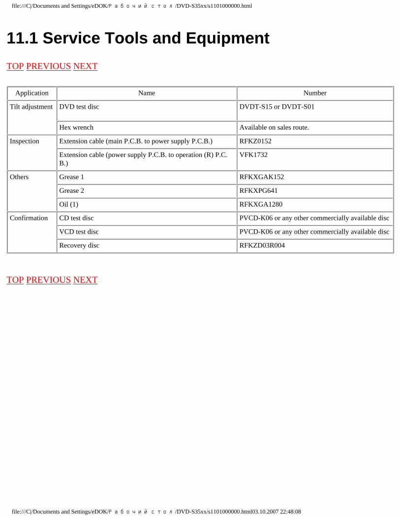
11.1 Service Tools and Equipment
TOP PREVIOUS NEXT
Application Name Number
Tilt adjustment DVD test disc DVDT-S15 or DVDT-S01
Hex wrench Available on sales route.
Inspection Extension cable (main P.C.B. to power supply P.C.B.) RFKZ0152
Extension cable (power supply P.C.B. to operation (R) P.C.B.)
VFK1732
Others Grease 1 RFKXGAK152
Grease 2 RFKXPG641
Oil (1) RFKXGA1280
Confirmation CD test disc PVCD-K06 or any other commercially available disc
VCD test disc PVCD-K06 or any other commercially available disc
Recovery disc RFKZD03R004
TOP PREVIOUS NEXT
file:///C|/Documents and Settings/eDOK/Рабочий стол/DVD-S35xx/s1101000000.html03.10.2007 22:48:08
file:///C|/Documents and Settings/eDOK/Рабочий стол/DVD-S35xx/s1102000000.html
11.2 Important points in adjustment
TOP PREVIOUS NEXT
11.2.1 Important points in optical adjustment
11.2.2 Important points in electrical adjustment
TOP PREVIOUS NEXT
file:///C|/Documents and Settings/eDOK/Рабочий стол/DVD-S35xx/s1102000000.html03.10.2007 22:48:12
file:///C|/Documents and Settings/eDOK/Рабочий стол/DVD-S35xx/s1102010000.html
11.2.1 Important points in optical adjustment
TOP PREVIOUS NEXT
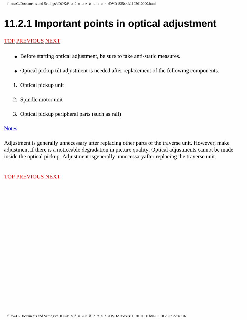
Before starting optical adjustment, be sure to take anti-static measures.
Optical pickup tilt adjustment is needed after replacement of the following components.
1. Optical pickup unit
2. Spindle motor unit
3. Optical pickup peripheral parts (such as rail)
Notes
Adjustment is generally unnecessary after replacing other parts of the traverse unit. However, make adjustment if there is a noticeable degradation in picture quality. Optical adjustments cannot be made inside the optical pickup. Adjustment isgenerally unnecessaryafter replacing the traverse unit.
TOP PREVIOUS NEXT
file:///C|/Documents and Settings/eDOK/Рабочий стол/DVD-S35xx/s1102010000.html03.10.2007 22:48:16
file:///C|/Documents and Settings/eDOK/Рабочий стол/DVD-S35xx/s1102020000.html
11.2.2 Important points in electrical adjustment
TOP PREVIOUS NEXT
Follow the adjustment procedures described in this Manual.
TOP PREVIOUS NEXT
file:///C|/Documents and Settings/eDOK/Рабочий стол/DVD-S35xx/s1102020000.html03.10.2007 22:48:20
file:///C|/Documents and Settings/eDOK/Рабочий стол/DVD-S35xx/s1103000000.html
11.3 Storing and Handling Test Discs
TOP PREVIOUS NEXT
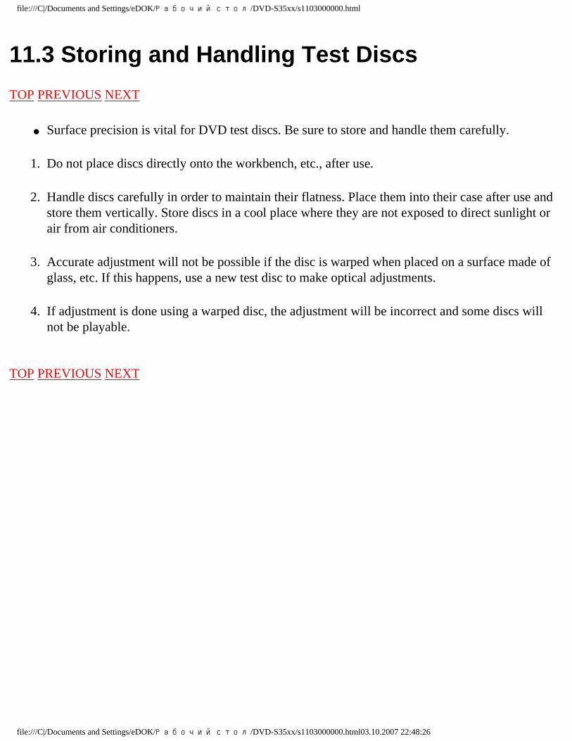
Surface precision is vital for DVD test discs. Be sure to store and handle them carefully.
1. Do not place discs directly onto the workbench, etc., after use.
2. Handle discs carefully in order to maintain their flatness. Place them into their case after use and store them vertically. Store discs in a cool place where they are not exposed to direct sunlight or air from air conditioners.
3. Accurate adjustment will not be possible if the disc is warped when placed on a surface made of glass, etc. If this happens, use a new test disc to make optical adjustments.
4. If adjustment is done using a warped disc, the adjustment will be incorrect and some discs will not be playable.
TOP PREVIOUS NEXT
file:///C|/Documents and Settings/eDOK/Рабочий стол/DVD-S35xx/s1103000000.html03.10.2007 22:48:26
file:///C|/Documents and Settings/eDOK/Рабочий стол/DVD-S35xx/s1104000000.html
11.4 Optical adjustment
TOP PREVIOUS NEXT
11.4.1 Optical pickup tilt adjustment
11.4.1.1 Adjustment procedure
11.4.1.2 Important points
11.4.1.3 Check after adjustment
11.4.1.4 Procedure for screw lock
TOP PREVIOUS NEXT
file:///C|/Documents and Settings/eDOK/Рабочий стол/DVD-S35xx/s1104000000.html03.10.2007 22:48:29
file:///C|/Documents and Settings/eDOK/Рабочий стол/DVD-S35xx/s1104010000.html
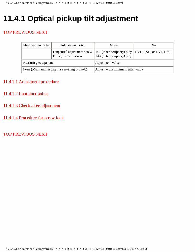
11.4.1 Optical pickup tilt adjustment
TOP PREVIOUS NEXT
Measurement point Adjustment point Mode Disc
Tangential adjustment screw Tilt adjustment screw
T01 (inner periphery) play T43 (outer periphery) play
DVDR-S15 or DVDT-S01
Measuring equipment Adjustment value
None (Main unit display for servicing is used.) Adjust to the minimum jitter value.
11.4.1.1 Adjustment procedure
11.4.1.2 Important points
11.4.1.3 Check after adjustment
11.4.1.4 Procedure for screw lock
TOP PREVIOUS NEXT
file:///C|/Documents and Settings/eDOK/Рабочий стол/DVD-S35xx/s1104010000.html03.10.2007 22:48:33
file:///C|/Documents and Settings/eDOK/Рабочий стол/DVD-S35xx/s1104010100.html
11.4.1.1 Adjustment procedure
TOP PREVIOUS NEXT
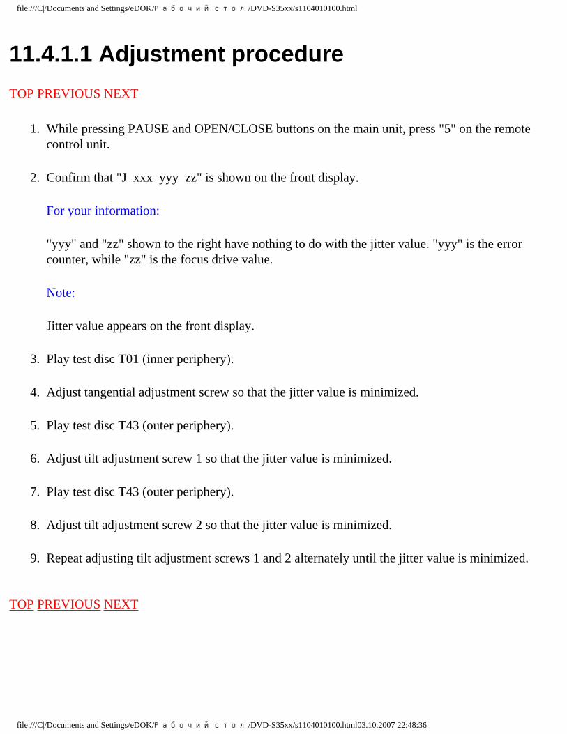
1. While pressing PAUSE and OPEN/CLOSE buttons on the main unit, press "5" on the remote control unit.
2. Confirm that "J_xxx_yyy_zz" is shown on the front display.
For your information:
"yyy" and "zz" shown to the right have nothing to do with the jitter value. "yyy" is the error counter, while "zz" is the focus drive value.
Note:
Jitter value appears on the front display.
3. Play test disc T01 (inner periphery).
4. Adjust tangential adjustment screw so that the jitter value is minimized.
5. Play test disc T43 (outer periphery).
6. Adjust tilt adjustment screw 1 so that the jitter value is minimized.
7. Play test disc T43 (outer periphery).
8. Adjust tilt adjustment screw 2 so that the jitter value is minimized.
9. Repeat adjusting tilt adjustment screws 1 and 2 alternately until the jitter value is minimized.
TOP PREVIOUS NEXT
file:///C|/Documents and Settings/eDOK/Рабочий стол/DVD-S35xx/s1104010100.html03.10.2007 22:48:36
file:///C|/Documents and Settings/eDOK/Рабочий стол/DVD-S35xx/s1104010200.html
11.4.1.2 Important points
TOP PREVIOUS NEXT
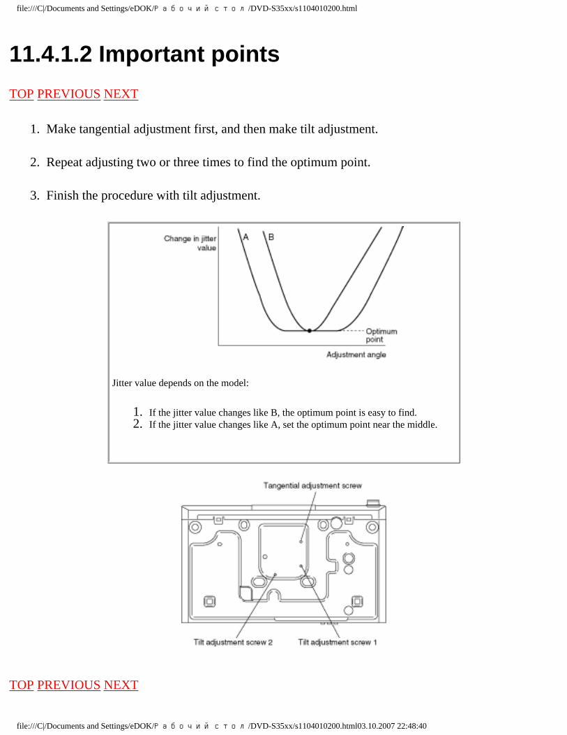
1. Make tangential adjustment first, and then make tilt adjustment.
2. Repeat adjusting two or three times to find the optimum point.
3. Finish the procedure with tilt adjustment.
Jitter value depends on the model:
1. If the jitter value changes like B, the optimum point is easy to find. 2. If the jitter value changes like A, set the optimum point near the middle.
TOP PREVIOUS NEXT
file:///C|/Documents and Settings/eDOK/Рабочий стол/DVD-S35xx/s1104010200.html03.10.2007 22:48:40
file:///C|/Documents and Settings/eDOK/Рабочий стол/DVD-S35xx/s1104010300.html
11.4.1.3 Check after adjustment
TOP PREVIOUS NEXT
Play test disc or any other disc to make sure there is no picture degradation in the inner, middle and outer peripheries, and no audio skipping. After adjustment is finished, lock each adjustment screw in position using screw lock.
TOP PREVIOUS NEXT
file:///C|/Documents and Settings/eDOK/Рабочий стол/DVD-S35xx/s1104010300.html03.10.2007 22:48:44
file:///C|/Documents and Settings/eDOK/Рабочий стол/DVD-S35xx/s1104010400.html
11.4.1.4 Procedure for screw lock
TOP PREVIOUS NEXT
1. After adjustment, remove top cover, tray, clamper base and traverse unit in this sequence.
2. Lay the traverse unit upside down, and fix adjustment screw with screw lock.
3. After fixing, reassemble traverse unit, clamper base, tray and top cover.
TOP PREVIOUS NEXT
file:///C|/Documents and Settings/eDOK/Рабочий стол/DVD-S35xx/s1104010400.html03.10.2007 22:48:47
file:///C|/Documents and Settings/eDOK/Рабочий стол/DVD-S35xx/s1200000000x.html
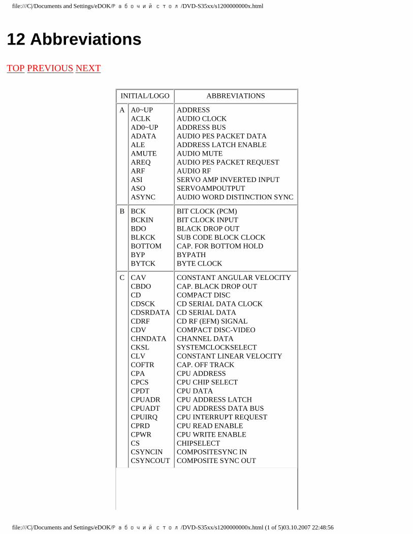
12 Abbreviations
TOP PREVIOUS NEXT
INITIAL/LOGO ABBREVIATIONS
A A0~UP ACLK AD0~UP ADATA ALE AMUTE AREQ ARF ASI ASO ASYNC
ADDRESS AUDIO CLOCK ADDRESS BUS AUDIO PES PACKET DATA ADDRESS LATCH ENABLE AUDIO MUTE AUDIO PES PACKET REQUEST AUDIO RF SERVO AMP INVERTED INPUT SERVOAMPOUTPUT AUDIO WORD DISTINCTION SYNC
B BCK BCKIN BDO BLKCK BOTTOM BYP BYTCK
BIT CLOCK (PCM) BIT CLOCK INPUT BLACK DROP OUT SUB CODE BLOCK CLOCK CAP. FOR BOTTOM HOLD BYPATH BYTE CLOCK
CONSTANT ANGULAR VELOCITY CAP. BLACK DROP OUT COMPACT DISC CD SERIAL DATA CLOCK CD SERIAL DATA CD RF (EFM) SIGNAL COMPACT DISC-VIDEO CHANNEL DATA SYSTEMCLOCKSELECT CONSTANT LINEAR VELOCITY CAP. OFF TRACK CPU ADDRESS CPU CHIP SELECT CPU DATA CPU ADDRESS LATCH CPU ADDRESS DATA BUS CPU INTERRUPT REQUEST CPU READ ENABLE CPU WRITE ENABLE CHIPSELECT COMPOSITESYNC IN COMPOSITE SYNC OUT
file:///C|/Documents and Settings/eDOK/Рабочий стол/DVD-S35xx/s1200000000x.html (1 of 5)03.10.2007 22:48:56
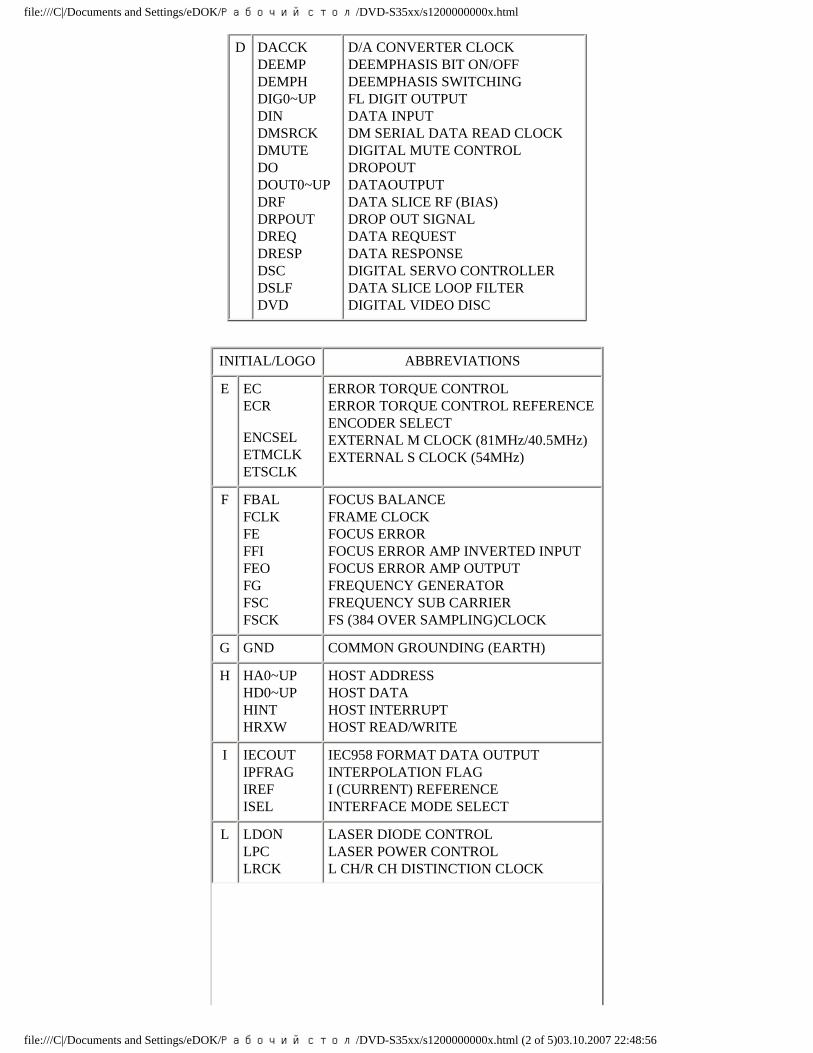
file:///C|/Documents and Settings/eDOK/Рабочий стол/DVD-S35xx/s1200000000x.html
D DACCK DEEMP DEMPH DIG0~UP DIN DMSRCK DMUTE DO DOUT0~UP DRF DRPOUT DREQ DRESP DSC DSLF DVD
D/A CONVERTER CLOCK DEEMPHASIS BIT ON/OFF DEEMPHASIS SWITCHING FL DIGIT OUTPUT DATA INPUT DM SERIAL DATA READ CLOCK DIGITAL MUTE CONTROL DROPOUT DATAOUTPUT DATA SLICE RF (BIAS) DROP OUT SIGNAL DATA REQUEST DATA RESPONSE DIGITAL SERVO CONTROLLER DATA SLICE LOOP FILTER DIGITAL VIDEO DISC
INITIAL/LOGO ABBREVIATIONS
E EC ECR ENCSEL ETMCLK ETSCLK
ERROR TORQUE CONTROL ERROR TORQUE CONTROL REFERENCE ENCODER SELECT EXTERNAL M CLOCK (81MHz/40.5MHz) EXTERNAL S CLOCK (54MHz)
F FBAL FCLK FE FFI FEO FG FSC FSCK
FOCUS BALANCE FRAME CLOCK FOCUS ERROR FOCUS ERROR AMP INVERTED INPUT FOCUS ERROR AMP OUTPUT FREQUENCY GENERATOR FREQUENCY SUB CARRIER FS (384 OVER SAMPLING)CLOCK
G GND COMMON GROUNDING (EARTH)
H HA0~UP HD0~UP HINT HRXW
HOST ADDRESS HOST DATA HOST INTERRUPT HOST READ/WRITE
I IECOUT IPFRAG IREF ISEL
IEC958 FORMAT DATA OUTPUT INTERPOLATION FLAG I (CURRENT) REFERENCE INTERFACE MODE SELECT
L LDON LPC LRCK
LASER DIODE CONTROL LASER POWER CONTROL L CH/R CH DISTINCTION CLOCK
file:///C|/Documents and Settings/eDOK/Рабочий стол/DVD-S35xx/s1200000000x.html (2 of 5)03.10.2007 22:48:56
file:///C|/Documents and Settings/eDOK/Рабочий стол/DVD-S35xx/s1200000000x.html
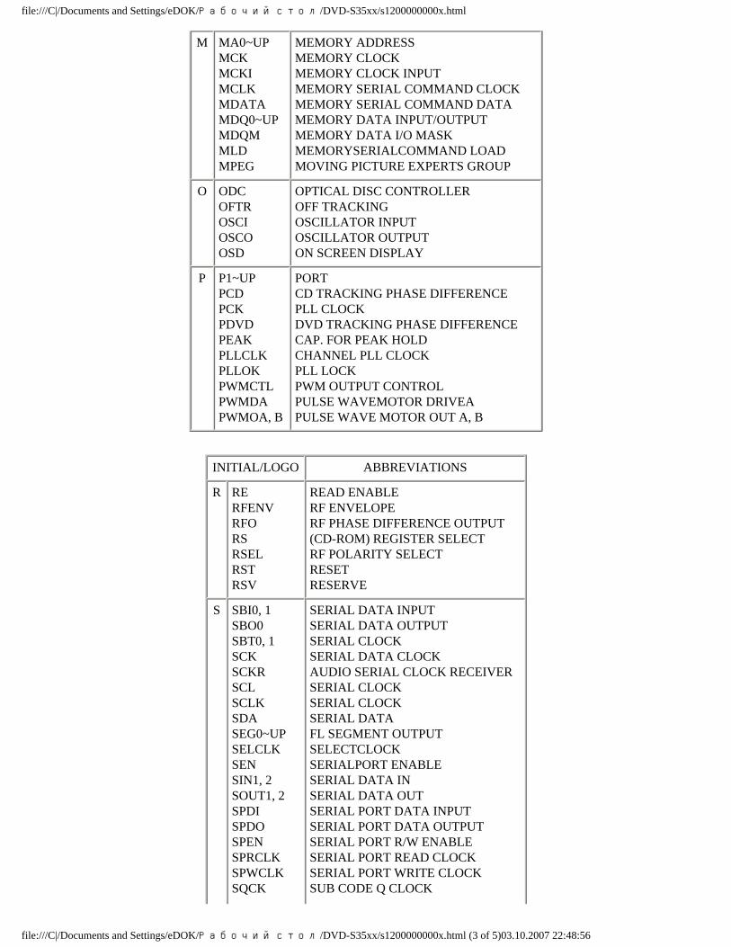
M MA0~UP MCK MCKI MCLK MDATA MDQ0~UP MDQM MLD MPEG
MEMORY ADDRESS MEMORY CLOCK MEMORY CLOCK INPUT MEMORY SERIAL COMMAND CLOCK MEMORY SERIAL COMMAND DATA MEMORY DATA INPUT/OUTPUT MEMORY DATA I/O MASK MEMORYSERIALCOMMAND LOAD MOVING PICTURE EXPERTS GROUP
O ODC OFTR OSCI OSCO OSD
OPTICAL DISC CONTROLLER OFF TRACKING OSCILLATOR INPUT OSCILLATOR OUTPUT ON SCREEN DISPLAY
P P1~UP PCD PCK PDVD PEAK PLLCLK PLLOK PWMCTL PWMDA PWMOA, B
PORT CD TRACKING PHASE DIFFERENCE PLL CLOCK DVD TRACKING PHASE DIFFERENCE CAP. FOR PEAK HOLD CHANNEL PLL CLOCK PLL LOCK PWM OUTPUT CONTROL PULSE WAVEMOTOR DRIVEA PULSE WAVE MOTOR OUT A, B
SERIAL DATA INPUT SERIAL DATA OUTPUT SERIAL CLOCK SERIAL DATA CLOCK AUDIO SERIAL CLOCK RECEIVER SERIAL CLOCK SERIAL CLOCK SERIAL DATA FL SEGMENT OUTPUT SELECTCLOCK SERIALPORT ENABLE SERIAL DATA IN SERIAL DATA OUT SERIAL PORT DATA INPUT SERIAL PORT DATA OUTPUT SERIAL PORT R/W ENABLE SERIAL PORT READ CLOCK SERIAL PORT WRITE CLOCK SUB CODE Q CLOCK
file:///C|/Documents and Settings/eDOK/Рабочий стол/DVD-S35xx/s1200000000x.html (3 of 5)03.10.2007 22:48:56
file:///C|/Documents and Settings/eDOK/Рабочий стол/DVD-S35xx/s1200000000x.html
SQCX SRDATA SRMADR SRMDT0~7 SS STAT STCLK STD0~UP STENABLE STSEL STVALID SUBC SBCK SUBQ SYSCLK
SUBCODEQ DATA READ CLOCK SERIAL DATA SRAM ADDRESS BUS SRAM DATA BUS 0~7 START/STOP STATUS STREAM DATA CLOCK STREAM DATA STREAM DATA INPUT ENABLE STREAM DATA POLARITY SELECT STREAMDATAVALIDITY SUB CODE SERIAL SUB CODE CLOCK SUB CODE Q DATA SYSTEM CLOCK
T TE TIBAL TID TIN TIP TIS TPSN TPSO TPSP TRCRS TRON TRSON
TRACKING ERROR BALANCE CONTROL BALANCE OUTPUT 1 BALANCE INPUT BALANCE INPUT BALANCE OUTPUT 2 OP AMP INPUT OP AMP OUTPUT OP AMP INVERTED INPUT TRACKCROSSSIGNAL TRACKING ON TRAVERSE SERVO ON
INITIAL/LOGO ABBREVIATIONS
V VBLANK VCC VCDCONT VDD VFB VREF VSS
V BLANKING COLLECTOR POWER SUPPLY VOLTAGE VIDEO CD CONTROL (TRACKING BALANCE) DRAIN POWER SUPPLY VOLTAGE VIDEO FEED BACK VOLTAGE REFERENCE SOURCE POWERSUPPLYVOLTAGE
W WAIT WDCK WEH WSR
BUS CYCLE WAIT WORD CLOCK WRITE ENABLE HIGH WORD SELECT RECEIVER
file:///C|/Documents and Settings/eDOK/Рабочий стол/DVD-S35xx/s1200000000x.html (4 of 5)03.10.2007 22:48:56
file:///C|/Documents and Settings/eDOK/Рабочий стол/DVD-S35xx/s1200000000x.html
X X XALE XAREQ XCDROM XCS XCSYNC XDS XHSYNCO XHINT XI XINT XMW XO XRE XSRMCE XSRMOE XSRMWE XVCS XVDS XVSYNCO
X´ TAL X ADDRESS LATCH ENABLE X AUDIO DATA REQUEST X CD ROM CHIP SELECT X CHIP SELECT X COMPOSITE SYNC X DATA STROBE X HORIZONTAL SYNC OUTPUT XHINTERRUPTREQUEST X´ TAL OSCILLATOR INPUT X INTERRUPT X MEMORY WRITE ENABLE X´ TAL OSCILLATOR OUTPUT X READ ENABLE X SRAM CHIP ENABLE X SRAM OUTPUT ENABLE X SRAM WRITE ENABLE XV-DEC CHIPSELECT X V-DEC CONTROL BUS STROBE X VERTICAL SYNC OUTPUT
TOP PREVIOUS NEXT
file:///C|/Documents and Settings/eDOK/Рабочий стол/DVD-S35xx/s1200000000x.html (5 of 5)03.10.2007 22:48:56
file:///C|/Documents and Settings/eDOK/Рабочий стол/DVD-S35xx/s1300000000x.html
13 VOLTAGE CHART
TOP PREVIOUS NEXT
Note:
Indicated voltage values are the atandard values for the unit measured by the DC electronic circuit tester (high-impedance) with the chassis taken as standard. Therefore, there may exist some errors in the voltage values, depending on theinternalimpedance of the DC circuit tester.
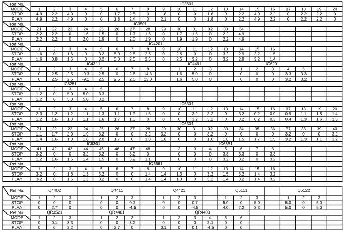
13.1 POWER SUPPLY P.C.B.
13.2 MAIN P.C.B.
13.3 OPERATION P.C.B.
TOP PREVIOUS NEXT
file:///C|/Documents and Settings/eDOK/Рабочий стол/DVD-S35xx/s1300000000x.html03.10.2007 22:49:07
file:///C|/Documents and Settings/eDOK/Рабочий стол/DVD-S35xx/s1301000000.html
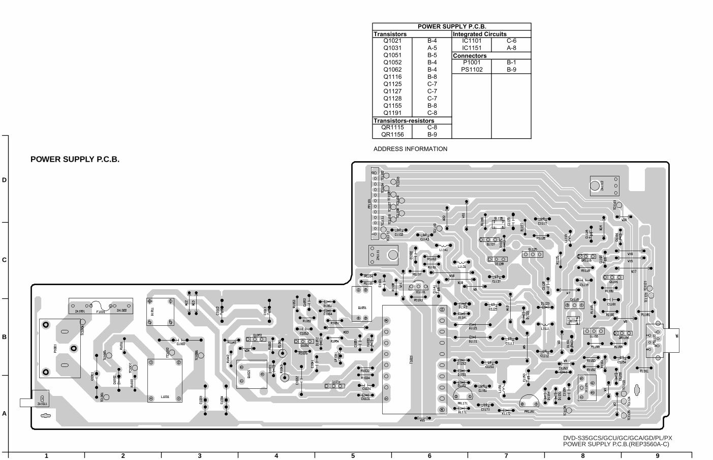
13.1 POWER SUPPLY P.C.B.
TOP PREVIOUS NEXT
TOP PREVIOUS NEXT
file:///C|/Documents and Settings/eDOK/Рабочий стол/DVD-S35xx/s1301000000.html03.10.2007 22:49:09
file:///C|/Documents and Settings/eDOK/Рабочий стол/DVD-S35xx/s1502000000.html
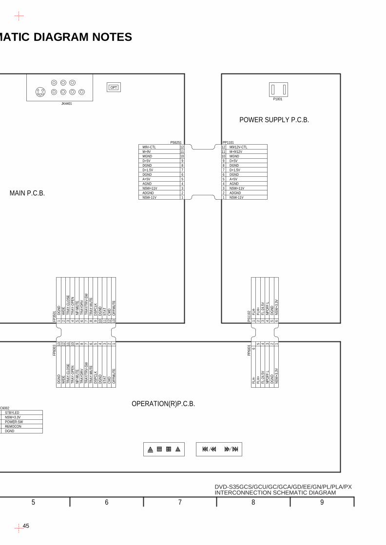
15.2 SCHEMATIC DIAGRAM NOTES
TOP PREVIOUS NEXT
This schematic diagram may be modified at any time with the development of new technology.
Important safety notice:
Components identified by mark have special characteristics important for safety.
Furthermore, special parts which have purpose of fire-retardant (resistors), high-quality sound (capacitors), low-noise (resistors), etc. are used. When replacing any of components, be sure to use only manufacture´s specified parts shownintheparts list.
Important safety notice:
There are special components used in this equipment which are important for safety.
These parts are marked by in the schematic diagrams. It is essential that these critical parts should be replaced with manufacturer’s specified parts to prevent shock, fire, or other hazards. Do not modify the original designwithoutpermission of manufacturer.
Caution!
IC and LSI are sensitive to static electricity.
Secondary trouble can be prevented by taking care during repair.
Cover the parts boxes made of plastics with aluminum foil.
Ground the soldering iron.
Put a conductive mat on the work table.
Do not touch the legs of IC or LSI with the fingers directly.
TOP PREVIOUS NEXT
file:///C|/Documents and Settings/eDOK/Рабочий стол/DVD-S35xx/s1502000000.html03.10.2007 22:50:53
file:///C|/Documents and Settings/eDOK/Рабочий стол/DVD-S35xx/s1600000000s.html
16 SCHEMATIC DIAGRAM
TOP PREVIOUS NEXT
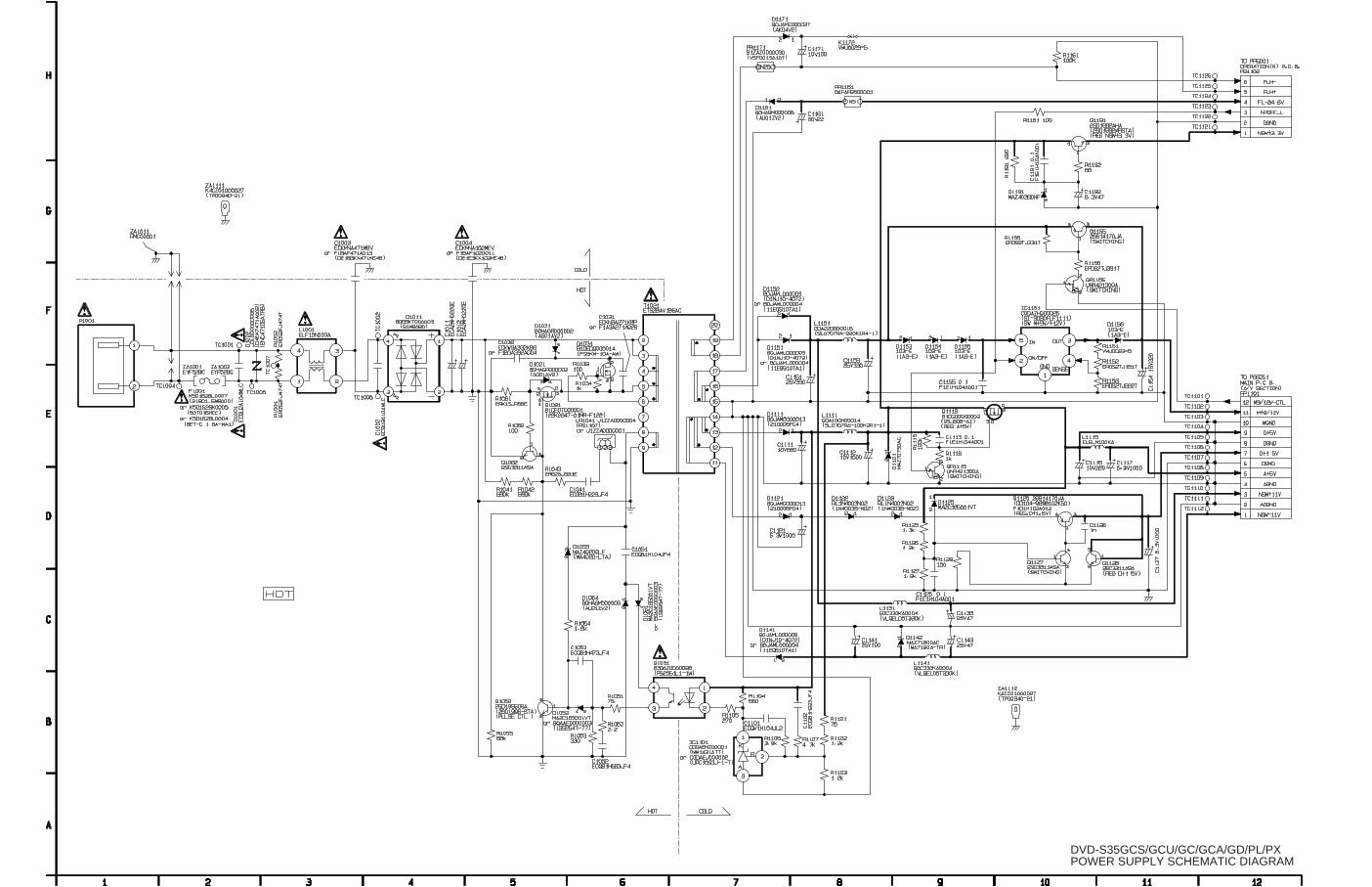
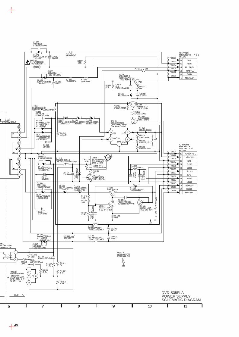
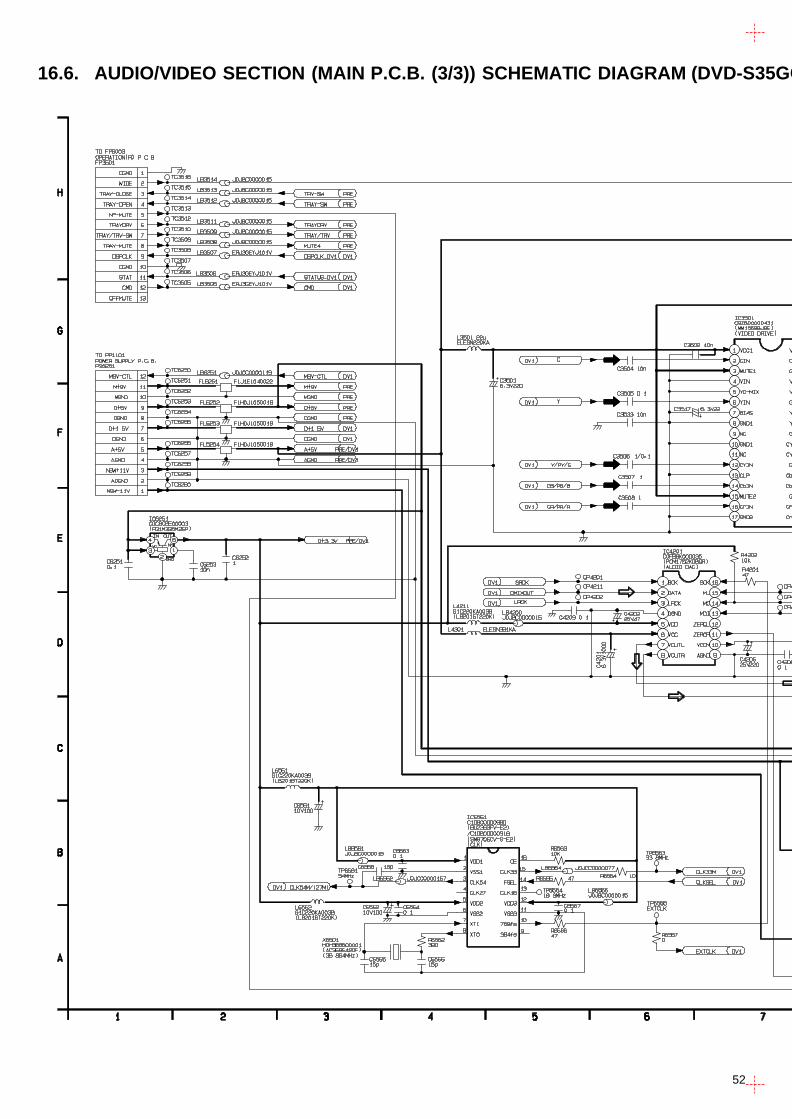
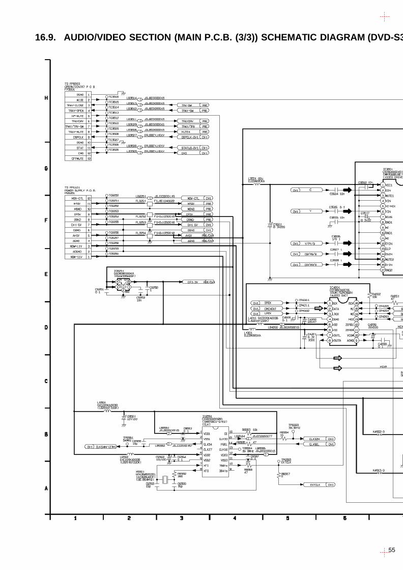
16.1 POWER SUPPLY SCHEMATIC DIAGRAM (DVD-S35GCS/GCU/GC/GCA/GD/PL/PX)
16.2 POWER SUPPLY SCHEMATIC DIAGRAM (DVD-S35EE/GN)
16.3 POWER SUPPLY SCHEMATIC DIAGRAM (DVD-S35PLA)
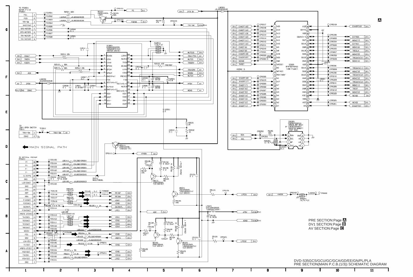
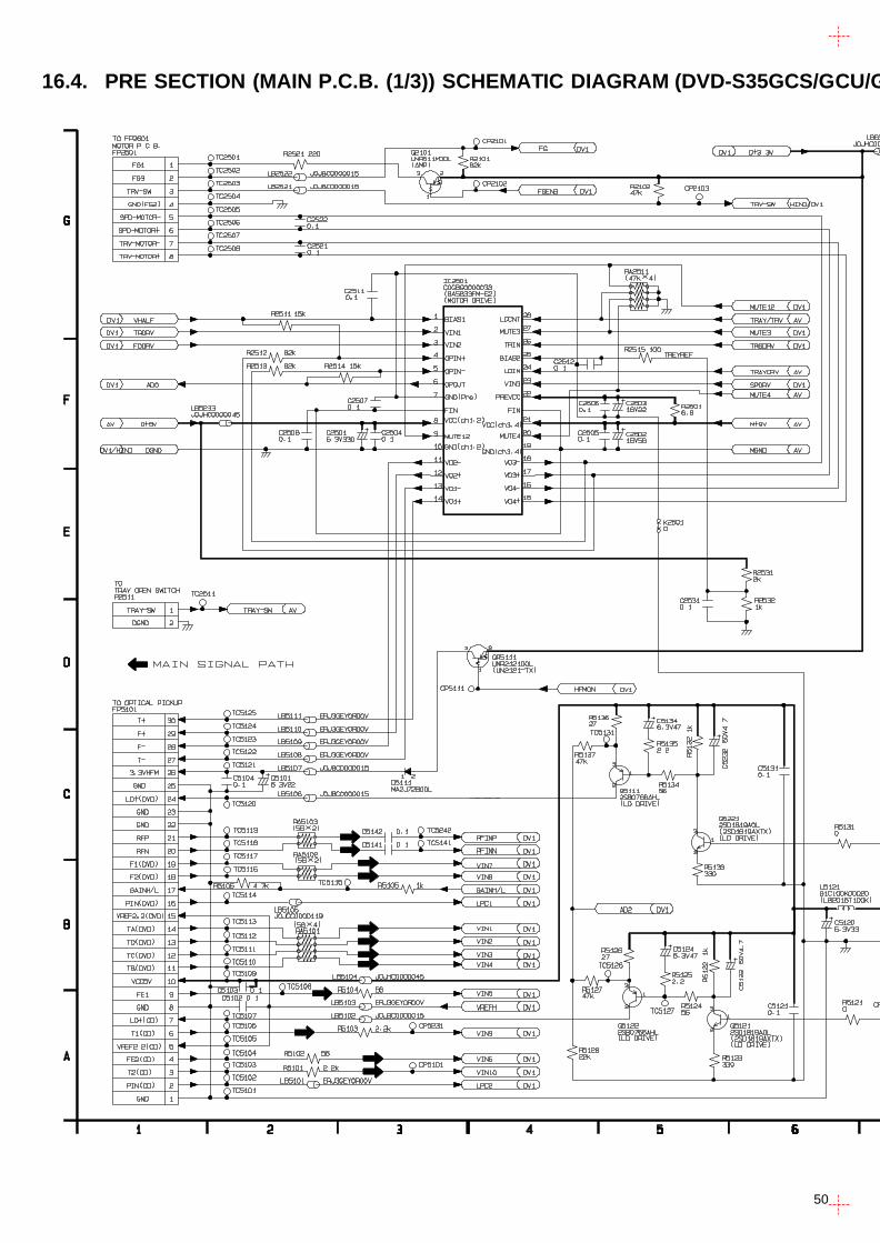
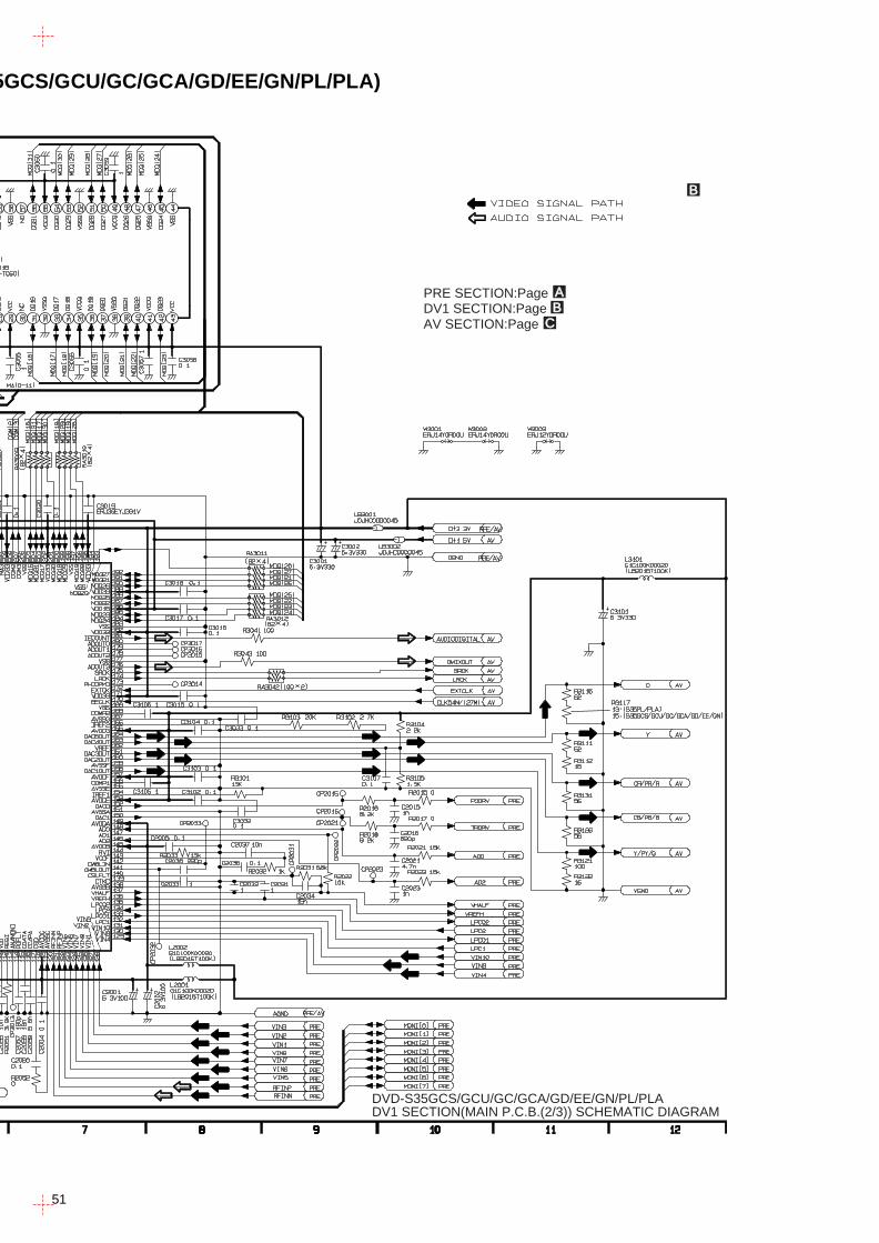
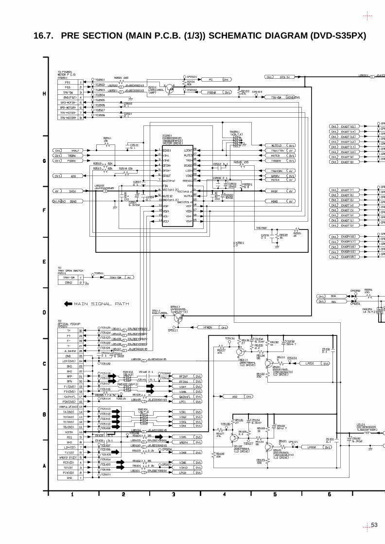
16.4 PRE SECTION (MAIN P.C.B. (1/3)) SCHEMATIC DIAGRAM (DVD-S35GCS/GCU/GC/GCA/GD/EE/GN/PL/PLA)
* IC6351 is not supplied in the form of an individual part.When replacing, be sure to replace the main p.c.b.and not IC6351 singly.
file:///C|/Documents and Settings/eDOK/Рабочий стол/DVD-S35xx/s1706000000.html
17.6 MAIN P.C.B. ADDRESS INFORMATION
TOP PREVIOUS NEXT
TOP PREVIOUS NEXT
file:///C|/Documents and Settings/eDOK/Рабочий стол/DVD-S35xx/s1706000000.html03.10.2007 22:53:33
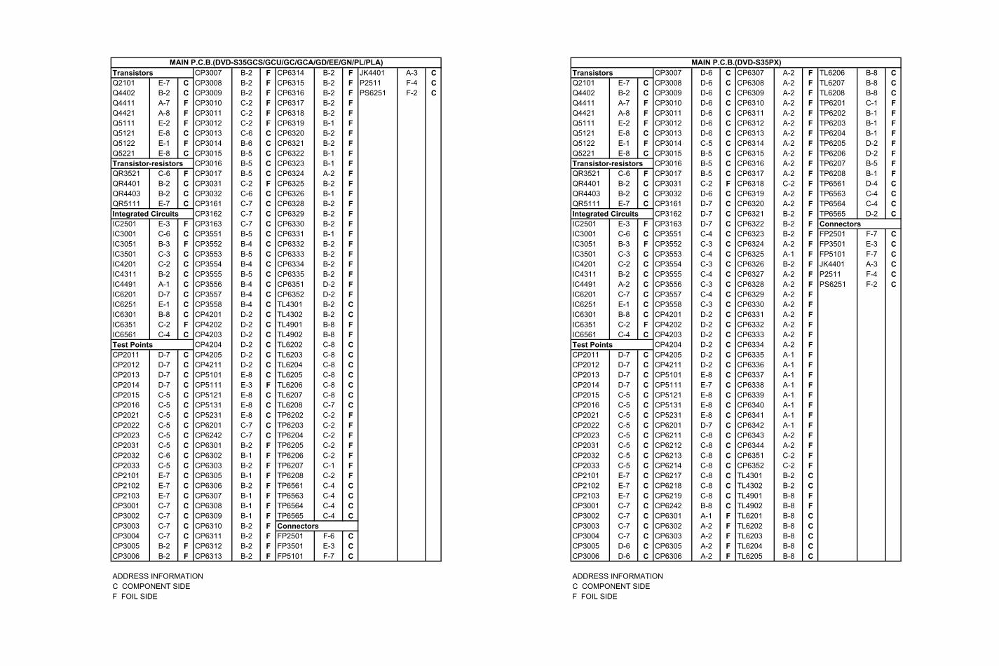
Transistors CP3007 B-2 F CP6314 B-2 F JK4401 A-3 CQ2101 E-7 C CP3008 B-2 F CP6315 B-2 F P2511 F-4 CQ4402 B-2 C CP3009 B-2 F CP6316 B-2 F PS6251 F-2 CQ4411 A-7 F CP3010 C-2 F CP6317 B-2 FQ4421 A-8 F CP3011 C-2 F CP6318 B-2 FQ5111 E-2 F CP3012 C-2 F CP6319 B-1 FQ5121 E-8 C CP3013 C-6 C CP6320 B-2 FQ5122 E-1 F CP3014 B-6 C CP6321 B-2 FQ5221 E-8 C CP3015 B-5 C CP6322 B-1 FTransistor-resistors CP3016 B-5 C CP6323 B-1 FQR3521 C-6 F CP3017 B-5 C CP6324 A-2 FQR4401 B-2 C CP3031 C-2 F CP6325 B-2 FQR4403 B-2 C CP3032 C-6 C CP6326 B-1 FQR5111 E-7 C CP3161 C-7 C CP6328 B-2 FIntegrated Circuits CP3162 C-7 C CP6329 B-2 FIC2501 E-3 F CP3163 C-7 C CP6330 B-2 FIC3001 C-6 C CP3551 B-5 C CP6331 B-1 FIC3051 B-3 F CP3552 B-4 C CP6332 B-2 FIC3501 C-3 C CP3553 B-5 C CP6333 B-2 FIC4201 C-2 C CP3554 B-4 C CP6334 B-2 FIC4311 B-2 C CP3555 B-5 C CP6335 B-2 FIC4491 A-1 C CP3556 B-4 C CP6351 D-2 FIC6201 D-7 C CP3557 B-4 C CP6352 D-2 FIC6251 E-1 C CP3558 B-4 C TL4301 B-2 CIC6301 B-8 C CP4201 D-2 C TL4302 B-2 CIC6351 C-2 F CP4202 D-2 C TL4901 B-8 FIC6561 C-4 C CP4203 D-2 C TL4902 B-8 FTest Points CP4204 D-2 C TL6202 C-8 CCP2011 D-7 C CP4205 D-2 C TL6203 C-8 CCP2012 D-7 C CP4211 D-2 C TL6204 C-8 CCP2013 D-7 C CP5101 E-8 C TL6205 C-8 CCP2014 D-7 C CP5111 E-3 F TL6206 C-8 CCP2015 C-5 C CP5121 E-8 C TL6207 C-8 CCP2016 C-5 C CP5131 E-8 C TL6208 C-7 CCP2021 C-5 C CP5231 E-8 C TP6202 C-2 FCP2022 C-5 C CP6201 C-7 C TP6203 C-2 FCP2023 C-5 C CP6242 C-7 C TP6204 C-2 FCP2031 C-5 C CP6301 B-2 F TP6205 C-2 FCP2032 C-6 C CP6302 B-1 F TP6206 C-2 FCP2033 C-5 C CP6303 B-2 F TP6207 C-1 FCP2101 E-7 C CP6305 B-1 F TP6208 C-2 FCP2102 E-7 C CP6306 B-2 F TP6561 C-4 CCP2103 E-7 C CP6307 B-1 F TP6563 C-4 CCP3001 C-7 C CP6308 B-1 F TP6564 C-4 CCP3002 C-7 C CP6309 B-1 F TP6565 C-4 CCP3003 C-7 C CP6310 B-2 F ConnectorsCP3004 C-7 C CP6311 B-2 F FP2501 F-6 CCP3005 B-2 F CP6312 B-2 F FP3501 E-3 CCP3006 B-2 F CP6313 B-2 F FP5101 F-7 C
ADDRESS INFORMATIONC COMPONENT SIDEF FOIL SIDE
MAIN P.C.B.(DVD-S35GCS/GCU/GC/GCA/GD/EE/GN/PL/PLA)Transistors CP3007 D-6 C CP6307 A-2 F TL6206 B-8 CQ2101 E-7 C CP3008 D-6 C CP6308 A-2 F TL6207 B-8 CQ4402 B-2 C CP3009 D-6 C CP6309 A-2 F TL6208 B-8 CQ4411 A-7 F CP3010 D-6 C CP6310 A-2 F TP6201 C-1 FQ4421 A-8 F CP3011 D-6 C CP6311 A-2 F TP6202 B-1 FQ5111 E-2 F CP3012 D-6 C CP6312 A-2 F TP6203 B-1 FQ5121 E-8 C CP3013 D-6 C CP6313 A-2 F TP6204 B-1 FQ5122 E-1 F CP3014 C-5 C CP6314 A-2 F TP6205 D-2 FQ5221 E-8 C CP3015 B-5 C CP6315 A-2 F TP6206 D-2 FTransistor-resistors CP3016 B-5 C CP6316 A-2 F TP6207 B-5 FQR3521 C-6 F CP3017 B-5 C CP6317 A-2 F TP6208 B-1 FQR4401 B-2 C CP3031 C-2 F CP6318 C-2 F TP6561 D-4 CQR4403 B-2 C CP3032 D-6 C CP6319 A-2 F TP6563 C-4 CQR5111 E-7 C CP3161 D-7 C CP6320 A-2 F TP6564 C-4 CIntegrated Circuits CP3162 D-7 C CP6321 B-2 F TP6565 D-2 CIC2501 E-3 F CP3163 D-7 C CP6322 B-2 F ConnectorsIC3001 C-6 C CP3551 C-4 C CP6323 B-2 F FP2501 F-7 CIC3051 B-3 F CP3552 C-3 C CP6324 A-2 F FP3501 E-3 CIC3501 C-3 C CP3553 C-4 C CP6325 A-1 F FP5101 F-7 CIC4201 C-2 C CP3554 C-3 C CP6326 B-2 F JK4401 A-3 CIC4311 B-2 C CP3555 C-4 C CP6327 A-2 F P2511 F-4 CIC4491 A-2 C CP3556 C-3 C CP6328 A-2 F PS6251 F-2 CIC6201 C-7 C CP3557 C-4 C CP6329 A-2 FIC6251 E-1 C CP3558 C-3 C CP6330 A-2 FIC6301 B-8 C CP4201 D-2 C CP6331 A-2 FIC6351 C-2 F CP4202 D-2 C CP6332 A-2 FIC6561 C-4 C CP4203 D-2 C CP6333 A-2 FTest Points CP4204 D-2 C CP6334 A-2 FCP2011 D-7 C CP4205 D-2 C CP6335 A-1 FCP2012 D-7 C CP4211 D-2 C CP6336 A-1 FCP2013 D-7 C CP5101 E-8 C CP6337 A-1 FCP2014 D-7 C CP5111 E-7 C CP6338 A-1 FCP2015 C-5 C CP5121 E-8 C CP6339 A-1 FCP2016 C-5 C CP5131 E-8 C CP6340 A-1 FCP2021 C-5 C CP5231 E-8 C CP6341 A-1 FCP2022 C-5 C CP6201 D-7 C CP6342 A-1 FCP2023 C-5 C CP6211 C-8 C CP6343 A-2 FCP2031 C-5 C CP6212 C-8 C CP6344 A-2 FCP2032 C-5 C CP6213 C-8 C CP6351 C-2 FCP2033 C-5 C CP6214 C-8 C CP6352 C-2 FCP2101 E-7 C CP6217 C-8 C TL4301 B-2 CCP2102 E-7 C CP6218 C-8 C TL4302 B-2 CCP2103 E-7 C CP6219 C-8 C TL4901 B-8 FCP3001 C-7 C CP6242 B-8 C TL4902 B-8 FCP3002 C-7 C CP6301 A-1 F TL6201 B-8 CCP3003 C-7 C CP6302 A-2 F TL6202 B-8 CCP3004 C-7 C CP6303 A-2 F TL6203 B-8 CCP3005 D-6 C CP6305 A-2 F TL6204 B-8 CCP3006 D-6 C CP6306 A-2 F TL6205 B-8 C
ADDRESS INFORMATIONC COMPONENT SIDEF FOIL SIDE
MAIN P.C.B.(DVD-S35PX)
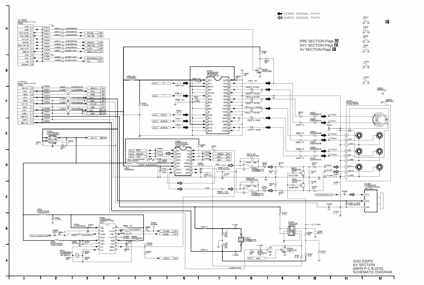
file:///C|/Documents and Settings/eDOK/Рабочий стол/DVD-S35xx/s1707000000.html
17.7 MAIN P.C.B. (1/2) (COMPONENT SIDE) (DVD-S35PX)
TOP PREVIOUS NEXT
TOP PREVIOUS NEXT
file:///C|/Documents and Settings/eDOK/Рабочий стол/DVD-S35xx/s1707000000.html03.10.2007 22:53:39
file:///C|/Documents and Settings/eDOK/Рабочий стол/DVD-S35xx/s1801000000.html03.10.2007 22:54:20
file:///C|/Documents and Settings/eDOK/Рабочий стол/DVD-S35xx/ob_cas_v.gif
file:///C|/Documents and Settings/eDOK/Рабочий стол/DVD-S35xx/ob_cas_v.gif (1 of 2)03.10.2007 22:54:24
file:///C|/Documents and Settings/eDOK/Рабочий стол/DVD-S35xx/ob_cas_v.gif
file:///C|/Documents and Settings/eDOK/Рабочий стол/DVD-S35xx/ob_cas_v.gif (2 of 2)03.10.2007 22:54:24
/DVD-S35xx/s1802000000.htmlстол Рабочийfile:///C|/Documents and Settings/eDOK/
18.2 Mechanism Section Exploded View
TOP PREVIOUS NEXT
TOP PREVIOUS NEXT
/DVD-S35xx/s1802000000.html03.10.2007 22:54:27стол Рабочийfile:///C|/Documents and Settings/eDOK/
file:///C|/Documents and Settings/eDOK/Рабочий стол/DVD-S35xx/ob_mec_v.gif
file:///C|/Documents and Settings/eDOK/Рабочий стол/DVD-S35xx/ob_mec_v.gif (1 of 2)03.10.2007 22:54:30
file:///C|/Documents and Settings/eDOK/Рабочий стол/DVD-S35xx/ob_mec_v.gif
file:///C|/Documents and Settings/eDOK/Рабочий стол/DVD-S35xx/ob_mec_v.gif (2 of 2)03.10.2007 22:54:30
file:///C|/Documents and Settings/eDOK/Рабочий стол/DVD-S35xx/s1803000000.html
18.3 Packing& Accessories Section Exploded View
TOP PREVIOUS NEXT
TOP PREVIOUS NEXT
file:///C|/Documents and Settings/eDOK/Рабочий стол/DVD-S35xx/s1803000000.html03.10.2007 22:54:34
/DVD-S35xx/ob_pac_v.gifстол Рабочийfile:///C|/Documents and Settings/eDOK/
/DVD-S35xx/ob_pac_v.gif (1 of 2)03.10.2007 22:54:37стол Рабочийfile:///C|/Documents and Settings/eDOK/
/DVD-S35xx/ob_pac_v.gifстол Рабочийfile:///C|/Documents and Settings/eDOK/
/DVD-S35xx/ob_pac_v.gif (2 of 2)03.10.2007 22:54:37стол Рабочийfile:///C|/Documents and Settings/eDOK/
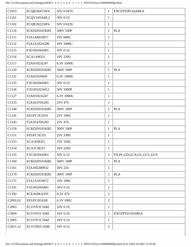
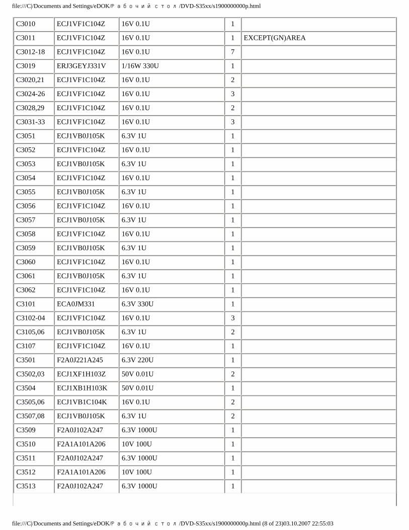
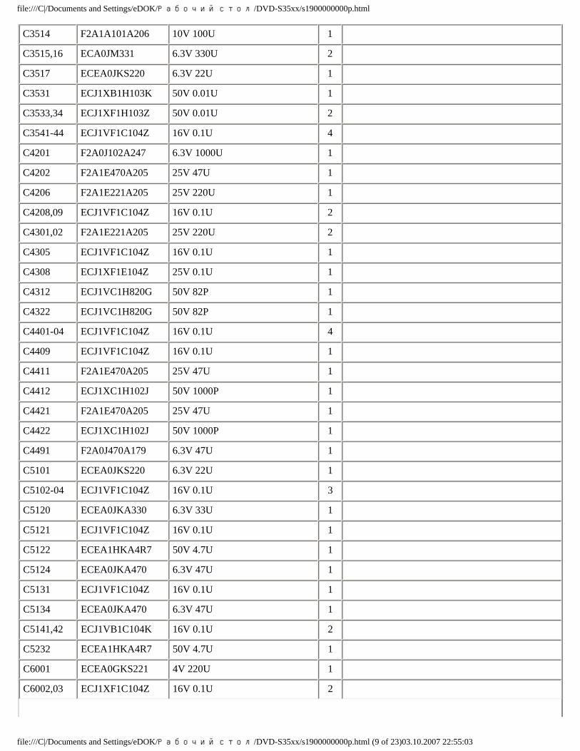
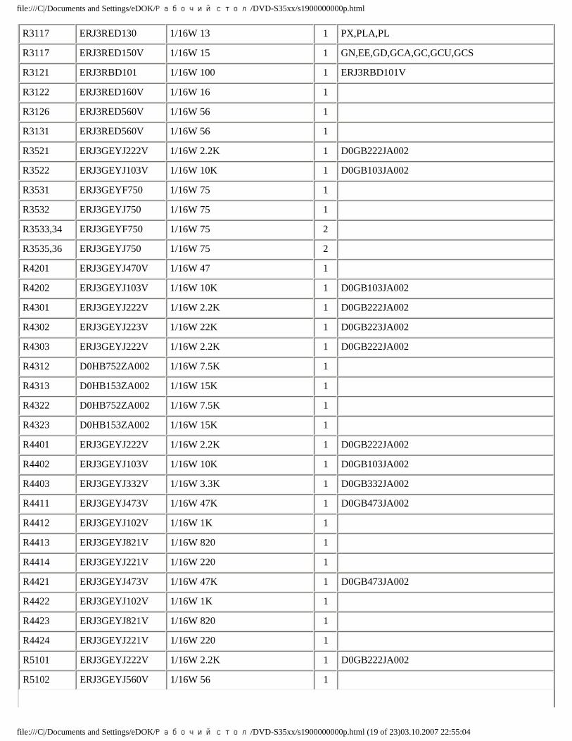
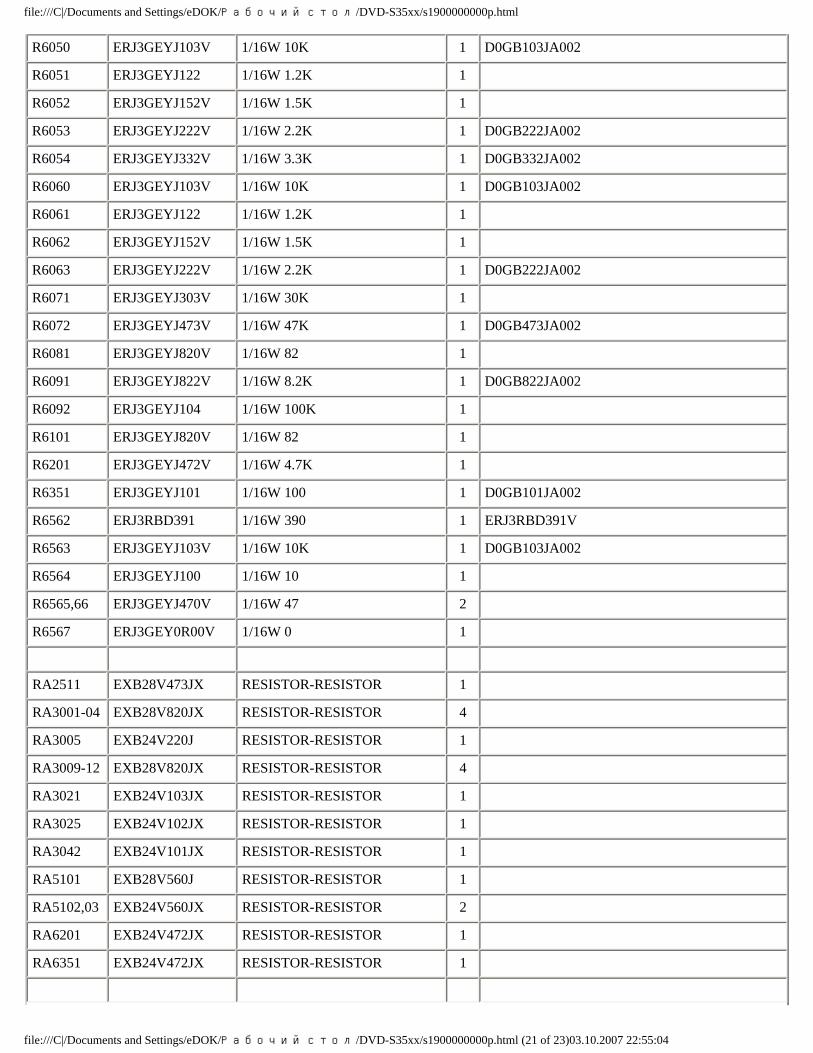
file:///C|/Documents and Settings/eDOK/Рабочий стол/DVD-S35xx/s1900000000p.html
19 REPLACEMENT PARTS LIST
TOP PREVIOUS NEXT
Notes:
*Important safety notice:
Components identified by mark have special characteristics important for safety.
Furthermore, special parts which have purposes of fire-retardant (resistors), high-quality sound (capacitors), low-noise (resistors), etc. are used.
When replacing any of components, be sure to use only manufacture’s specified parts shown in the parts list.
*Warning: This product uses a laser diode. Refer to caution statements.
*Capacity values are in microfarads (μF) unless specified otherwise, P=Pico-farads (pF), F=Farads (F).
*Resistance values are in ohms, unless specified otherwise, 1K=1,000 (OHM), 1M=1,000k (OHM).
*The marking (RTL) indicates the retention time is limited for this item. After the discontinuation of this assembly in production, it will no longer be available.
*“<IA> - <IF>”, marks in Remarks indicate languages of instruction manuals. [<IA>: English, <IB>: English, <IC>: Spanish, Portuguese, <ID>:Chinese, <IE>:Korean, <IF>: Arabic.]
*All parts are supplied by S.P.C..
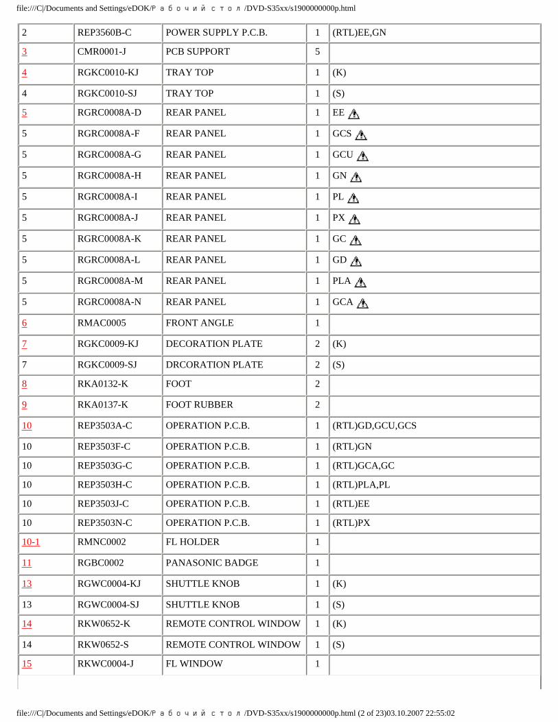
Ref. No. Part No. Part Name & Description Pcs Remarks
1 REP3579E-C MAIN P.C.B. 1 PX
1 REP3580D-C MAIN P.C.B. 1 PLA,PL
1 REP3580F-C MAIN P.C.B. 1 GN,EE,GD,GCA,GC,GCU,GCS
2 REP3504C-1C POWER SUPPLY P.C.B. 1 (RTL)PLA
2 REP3560A-C POWER SUPPLY P.C.B. 1 (RTL)PX,PL,GD,GCA,GC,GCU,GCS
file:///C|/Documents and Settings/eDOK/Рабочий стол/DVD-S35xx/s1900000000p.html (1 of 23)03.10.2007 22:55:02
file:///C|/Documents and Settings/eDOK/Рабочий стол/DVD-S35xx/s1900000000p.html
2 REP3560B-C POWER SUPPLY P.C.B. 1 (RTL)EE,GN
3 CMR0001-J PCB SUPPORT 5
4 RGKC0010-KJ TRAY TOP 1 (K)
4 RGKC0010-SJ TRAY TOP 1 (S)
5 RGRC0008A-D REAR PANEL 1 EE
5 RGRC0008A-F REAR PANEL 1 GCS
5 RGRC0008A-G REAR PANEL 1 GCU
5 RGRC0008A-H REAR PANEL 1 GN
5 RGRC0008A-I REAR PANEL 1 PL
5 RGRC0008A-J REAR PANEL 1 PX
5 RGRC0008A-K REAR PANEL 1 GC
5 RGRC0008A-L REAR PANEL 1 GD
5 RGRC0008A-M REAR PANEL 1 PLA
5 RGRC0008A-N REAR PANEL 1 GCA
6 RMAC0005 FRONT ANGLE 1
7 RGKC0009-KJ DECORATION PLATE 2 (K)
7 RGKC0009-SJ DRCORATION PLATE 2 (S)
8 RKA0132-K FOOT 2
9 RKA0137-K FOOT RUBBER 2
10 REP3503A-C OPERATION P.C.B. 1 (RTL)GD,GCU,GCS
10 REP3503F-C OPERATION P.C.B. 1 (RTL)GN
10 REP3503G-C OPERATION P.C.B. 1 (RTL)GCA,GC
10 REP3503H-C OPERATION P.C.B. 1 (RTL)PLA,PL
10 REP3503J-C OPERATION P.C.B. 1 (RTL)EE
10 REP3503N-C OPERATION P.C.B. 1 (RTL)PX
10-1 RMNC0002 FL HOLDER 1
11 RGBC0002 PANASONIC BADGE 1
13 RGWC0004-KJ SHUTTLE KNOB 1 (K)
13 RGWC0004-SJ SHUTTLE KNOB 1 (S)
14 RKW0652-K REMOTE CONTROL WINDOW 1 (K)
14 RKW0652-S REMOTE CONTROL WINDOW 1 (S)
15 RKWC0004-J FL WINDOW 1
file:///C|/Documents and Settings/eDOK/Рабочий стол/DVD-S35xx/s1900000000p.html (2 of 23)03.10.2007 22:55:02
file:///C|/Documents and Settings/eDOK/Рабочий стол/DVD-S35xx/s1900000000p.html
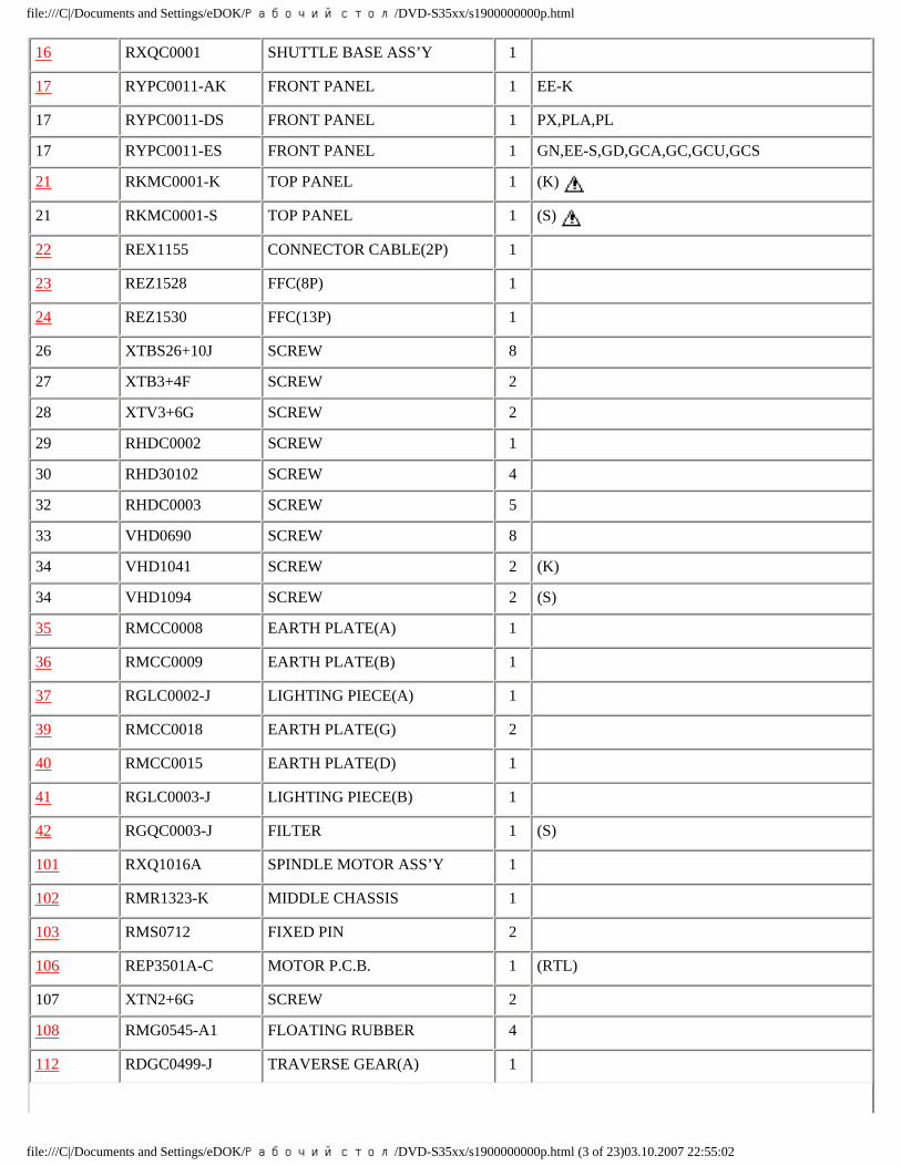
16 RXQC0001 SHUTTLE BASE ASS’Y 1
17 RYPC0011-AK FRONT PANEL 1 EE-K
17 RYPC0011-DS FRONT PANEL 1 PX,PLA,PL
17 RYPC0011-ES FRONT PANEL 1 GN,EE-S,GD,GCA,GC,GCU,GCS
21 RKMC0001-K TOP PANEL 1 (K)
21 RKMC0001-S TOP PANEL 1 (S)
22 REX1155 CONNECTOR CABLE(2P) 1
23 REZ1528 FFC(8P) 1
24 REZ1530 FFC(13P) 1
26 XTBS26+10J SCREW 8
27 XTB3+4F SCREW 2
28 XTV3+6G SCREW 2
29 RHDC0002 SCREW 1
30 RHD30102 SCREW 4
32 RHDC0003 SCREW 5
33 VHD0690 SCREW 8
34 VHD1041 SCREW 2 (K)
34 VHD1094 SCREW 2 (S)
35 RMCC0008 EARTH PLATE(A) 1
36 RMCC0009 EARTH PLATE(B) 1
37 RGLC0002-J LIGHTING PIECE(A) 1
39 RMCC0018 EARTH PLATE(G) 2
40 RMCC0015 EARTH PLATE(D) 1
41 RGLC0003-J LIGHTING PIECE(B) 1
42 RGQC0003-J FILTER 1 (S)
101 RXQ1016A SPINDLE MOTOR ASS’Y 1
102 RMR1323-K MIDDLE CHASSIS 1
103 RMS0712 FIXED PIN 2
106 REP3501A-C MOTOR P.C.B. 1 (RTL)
107 XTN2+6G SCREW 2
108 RMG0545-A1 FLOATING RUBBER 4
112 RDGC0499-J TRAVERSE GEAR(A) 1
file:///C|/Documents and Settings/eDOK/Рабочий стол/DVD-S35xx/s1900000000p.html (3 of 23)03.10.2007 22:55:02
file:///C|/Documents and Settings/eDOK/Рабочий стол/DVD-S35xx/s1900000000p.html
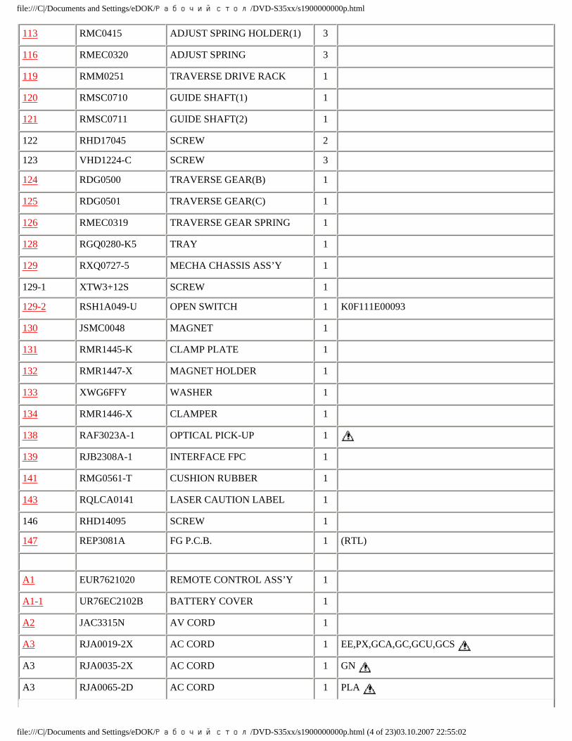
113 RMC0415 ADJUST SPRING HOLDER(1) 3
116 RMEC0320 ADJUST SPRING 3
119 RMM0251 TRAVERSE DRIVE RACK 1
120 RMSC0710 GUIDE SHAFT(1) 1
121 RMSC0711 GUIDE SHAFT(2) 1
122 RHD17045 SCREW 2
123 VHD1224-C SCREW 3
124 RDG0500 TRAVERSE GEAR(B) 1
125 RDG0501 TRAVERSE GEAR(C) 1
126 RMEC0319 TRAVERSE GEAR SPRING 1
128 RGQ0280-K5 TRAY 1
129 RXQ0727-5 MECHA CHASSIS ASS’Y 1
129-1 XTW3+12S SCREW 1
129-2 RSH1A049-U OPEN SWITCH 1 K0F111E00093
130 JSMC0048 MAGNET 1
131 RMR1445-K CLAMP PLATE 1
132 RMR1447-X MAGNET HOLDER 1
133 XWG6FFY WASHER 1
134 RMR1446-X CLAMPER 1
138 RAF3023A-1 OPTICAL PICK-UP 1
139 RJB2308A-1 INTERFACE FPC 1
141 RMG0561-T CUSHION RUBBER 1
143 RQLCA0141 LASER CAUTION LABEL 1
146 RHD14095 SCREW 1
147 REP3081A FG P.C.B. 1 (RTL)
A1 EUR7621020 REMOTE CONTROL ASS’Y 1
A1-1 UR76EC2102B BATTERY COVER 1
A2 JAC3315N AV CORD 1
A3 RJA0019-2X AC CORD 1 EE,PX,GCA,GC,GCU,GCS
A3 RJA0035-2X AC CORD 1 GN
A3 RJA0065-2D AC CORD 1 PLA
file:///C|/Documents and Settings/eDOK/Рабочий стол/DVD-S35xx/s1900000000p.html (4 of 23)03.10.2007 22:55:02
file:///C|/Documents and Settings/eDOK/Рабочий стол/DVD-S35xx/s1900000000p.html
This schematic diagram may be modified at any time with the development of new technology.
Important safety notice:
Components identified by mark have special characteristics important for safety.
Furthermore, special parts which have purpose of fire-retardant (resistors), high-quality sound (capacitors), low-noise(resistors), etc. are used. When replacing any of components, be sure to use only manufacture´s specified parts shown intheparts list.
Important safety notice:
There are special components used in this equipment which are important for safety.
These parts are marked by in the schematic diagrams. It is essential that these critical parts should be replaced withmanufacturer’s specified parts to prevent shock, fire, or other hazards. Do not modify the original design without permission ofmanufacturer.
Caution!
IC and LSI are sensitive to static electricity.
Secondary trouble can be prevented by taking care during repair.
Cover the parts boxes made of plastics with aluminum foil.
Ground the soldering iron.
Put a conductive mat on the work table.
Do not touch the legs of IC or LSI with the fingers directly.
15.2. SCHEMATIC DIAGRAM NOTES
46
16 SCHEMATIC DIAGRAM
16.1. POWER SUPPLY SCHEMATIC DIAGRAM (DVD-S35GCS/GCU/GC/GCA/GD/PL/PX)