•VLSI Design I; A. Milenkovic •1 CPE/EE 427, CPE 527 VLSI Design I L21: Sequential Circuits Department of Electrical and Computer Engineering University of Alabama in Huntsville Aleksandar Milenkovic ( www.ece.uah.edu/~milenka ) www.ece.uah.edu/~milenka/cpe527-05F 11/7/2005 VLSI Design I; A. Milenkovic 2 Review: The Regenerative Property If the gain in the transient region is larger than 1, only A and B are stable operation points. C is a metastable operation point. A V i2 V o2 V i1 = V o2 V i 2 = V o 1 B C V o1 V i1 cascaded inverters
Transcript
•VLSI Design I; A. Milenkovic •1
CPE/EE 427, CPE 527 VLSI Design I
L21: Sequential Circuits
Department of Electrical and Computer Engineering University of Alabama in Huntsville
Aleksandar Milenkovic ( www.ece.uah.edu/~milenka )www.ece.uah.edu/~milenka/cpe527-05F
11/7/2005 VLSI Design I; A. Milenkovic 2
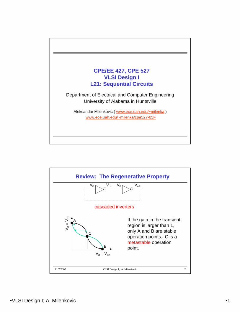
Review: The Regenerative Property
If the gain in the transient region is larger than 1, only A and B are stable operation points. C is a metastable operation point.
A
Vi2 Vo2
Vi1 = Vo2
V i2 =
V o1
B
C
Vo1Vi1
cascaded inverters
•VLSI Design I; A. Milenkovic •2
11/7/2005 VLSI Design I; A. Milenkovic 3
Bistable Circuits
• The cross-coupling of two inverters results in a bistablecircuit (a circuit with two stable states)
• Have to be able to change the stored value by making A (or B) temporarily unstable by increasing the loop gain to a value larger than 1– done by applying a trigger pulse at Vi1 or Vi2
– the width of the trigger pulse need be only a little larger than the total propagation delay around the loop circuit (twice the delay of an inverter)
• Two approaches used– cutting the feedback loop (mux based latch)– overpowering the feedback loop (as used in SRAMs)
Vi1
Vi2
11/7/2005 VLSI Design I; A. Milenkovic 4
Review: SR Latch
disallowed0011
reset1010
set0101
memory!QQ00
!QQRSS
RQ
!Q
•VLSI Design I; A. Milenkovic •3
11/7/2005 VLSI Design I; A. Milenkovic 5
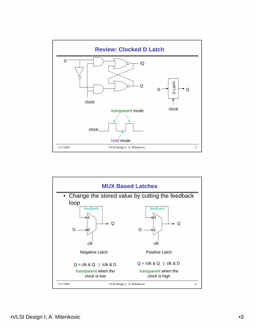
Review: Clocked D Latch
clock
D L
atch
QD
D
Q
!Q
clock
clock
transparent mode
hold mode
11/7/2005 VLSI Design I; A. Milenkovic 6
MUX Based Latches
QD
clk
0
1
Positive Latch
QD
clk
1
0
Negative Latch
Q = !clk & Q | clk & DQ = clk & Q | !clk & D
feedback
transparent when the clock is low
transparent when the clock is high
feedback
• Change the stored value by cutting the feedback loop
•VLSI Design I; A. Milenkovic •4
11/7/2005 VLSI Design I; A. Milenkovic 7
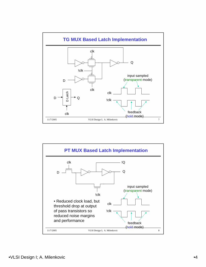
TG MUX Based Latch Implementation
Q
D
clk
clk
!clk
!clk
clk
input sampled(transparent mode)
feedback(hold mode)
clk
D L
atch
QD
11/7/2005 VLSI Design I; A. Milenkovic 8
PT MUX Based Latch Implementation
QD
clk !Q
!clk
!clk
clk
input sampled(transparent mode)
feedback(hold mode)
• Reduced clock load, but threshold drop at output of pass transistors so reduced noise margins and performance
•VLSI Design I; A. Milenkovic •5
11/7/2005 VLSI Design I; A. Milenkovic 9
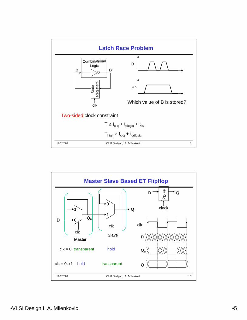
Latch Race Problem
CombinationalLogic
clk
Sta
teR
egis
ters
clk
B B’
Two-sided clock constraint
T ≥ tc-q + tplogic + tsu
Thigh < tc-q + tcdlogic
B
Which value of B is stored?
11/7/2005 VLSI Design I; A. Milenkovic 10
Master Slave Based ET Flipflop
QMD 0
1 Q1
0
SlaveMaster
QMD
clk
0
1 Q
clk
1
0
SlaveMaster
clk
QM
Q
D
clock
D F
F
QD
clk = 0 transparent hold
clk = 0→1 hold transparent
•VLSI Design I; A. Milenkovic •6
11/7/2005 VLSI Design I; A. Milenkovic 11
MS ET Implementation
Q
D
clk
QM
I1
I2 I3
I4
I5 I6T2
T1T3
T4
Master Slave
!clk
clk
11/7/2005 VLSI Design I; A. Milenkovic 12
MS ET Implementation
Q
D
clk
QM
I1
I2 I3
I4
I5 I6T2
T1T3
T4
Master Slave
!clk
clk
master transparentslave hold
master holdslave transparent
•VLSI Design I; A. Milenkovic •7
11/7/2005 VLSI Design I; A. Milenkovic 13
MS ET Timing Properties
• Assume propagation delays are tpd_inv and tpd_tx, that the contamination delay is 0, and that the inverter delay to derive !clk is 0
• Set-up time - time before rising edge of clk that D must be valid
• Propagation delay - time for QM to reach Q
• Hold time - time D must be stable after rising edge of clk -
11/7/2005 VLSI Design I; A. Milenkovic 14
MS ET Timing Properties
• Assume propagation delays are tpd_inv and tpd_tx, that the contamination delay is 0, and that the inverter delay to derive !clk is 0
• Set-up time - time before rising edge of clk that D must be valid
• Propagation delay - time for QM to reach Q
• Hold time - time D must be stable after rising edge of clk
3 * tpd_inv + tpd_tx
tpd_inv + tpd_tx
zero
•VLSI Design I; A. Milenkovic •8
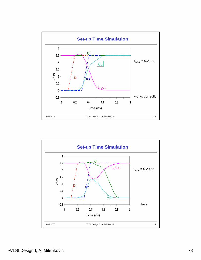
11/7/2005 VLSI Design I; A. Milenkovic 15
Set-up Time Simulation
-0.5
0
0.5
1
1.5
2
2.5
3
0 0.2 0.4 0.6 0.8 1
Vol
ts
Time (ns)
D clk
Q
QM
I2 out
tsetup = 0.21 ns
works correctly
11/7/2005 VLSI Design I; A. Milenkovic 16
Set-up Time Simulation
-0.5
0
0.5
1
1.5
2
2.5
3
0 0.2 0.4 0.6 0.8 1
Vol
ts
Time (ns)
D clk
Q
QM
I2 out tsetup = 0.20 ns
fails
•VLSI Design I; A. Milenkovic •9
11/7/2005 VLSI Design I; A. Milenkovic 17
Propagation Delay Simulation
-0.5
0
0.5
1
1.5
2
2.5
3
0 0.5 1 1.5 2 2.5
Vol
ts
Time (ns)
tc-q(LH) = 160 psec
tc-q(HL) = 180 psectc-q(LH) tc-q(HL)
11/7/2005 VLSI Design I; A. Milenkovic 18
Reduced Load MS ET FF
!clkclk
QD
!clk clk
I1
I2 I4
I3QM T2T1
reverse conduction
• Clock load per register is important since it directly impacts the power dissipation of the clock network.
• Can reduce the clock load (at the cost of robustness) by making the circuit ratioed
– to switch the state of the master, T1 must be sized to overpower I2– to avoid reverse conduction, I4 must be weaker than I1
•VLSI Design I; A. Milenkovic •10
11/7/2005 VLSI Design I; A. Milenkovic 19
Non-Ideal Clocks
!clk
clk
Ideal clocks
!clk
clk
Non-ideal clocksclock skew
1-1 overlap
0-0 overlap
11/7/2005 VLSI Design I; A. Milenkovic 20
Example of Clock Skew Problems
D
clk X
!clk
!Q
!clk Q
clk
B
AP1
P2
P3
P4
I1 I2 I3 I4
Race condition – direct path from D to Q during the short time when both clk and !clk are high (1-1 overlap)
Undefined state – both B and D are driving A when clkand !clk are both highDynamic storage – when clk and !clk are both low (0-0 overlap)
•VLSI Design I; A. Milenkovic •11
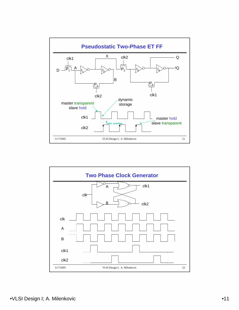
11/7/2005 VLSI Design I; A. Milenkovic 21
Pseudostatic Two-Phase ET FF
D
clk1 X
clk2
!Q
clk2 Q
clk1
B
AP1
P2
P3
P4
I1 I2 I3 I4
clk2
clk1
master transparentslave hold
master holdslave transparent
dynamicstorage
tnon_overlap
11/7/2005 VLSI Design I; A. Milenkovic 22
Two Phase Clock Generator
clk
clk1
clk2
A
clk
A
B
B
clk1
clk2
•VLSI Design I; A. Milenkovic •12
11/7/2005 VLSI Design I; A. Milenkovic 23
Power PC Flipflop
D Q
clk
!clk
!clk
clk
01
10 1
!clk
clk
11/7/2005 VLSI Design I; A. Milenkovic 24
Power PC Flipflop
D Q
clk
!clk
!clk
clk
01
10 1
!clk
clk
master transparentslave hold
master holdslave transparent
→0→1 →0 →1
•VLSI Design I; A. Milenkovic •13
11/7/2005 VLSI Design I; A. Milenkovic 25
Ratioed CMOS Clocked SR Latch
1
10
0
onoff
on
off
off
onM1
S R
clkclk
!QQ
M2
M3
M4
M5
M6
M7
M8
11/7/2005 VLSI Design I; A. Milenkovic 26
Ratioed CMOS Clocked SR Latch
1
10
0
onoff
off->onoff->on
→ 0
1 ←
on
off
off
on
→ on
→ on
→ off
→ offM1
S R
clkclk
!QQ
M2
M3
M4
M5
M6
M7
M8 0 → 10 → 1
•VLSI Design I; A. Milenkovic •14
11/7/2005 VLSI Design I; A. Milenkovic 27
Sizing Issues
0
0.5
1
1.5
2
2 2.5 3 3.5 4W/L5and6
!Q (V
olts
)
W/L2and4 = 1.5µm/0.25 µm
W/L1and3 = 0.5µm/0.25 µm
so W/L5and6 > 3
11/7/2005 VLSI Design I; A. Milenkovic 28
Transient Response
0
1
2
3
0.9 1 1.1 1.2 1.3 1.4 1.5
Q &
!Q (V
olts
)
SET
!QQ
Time (ns)
tc-!Q tc-Q
•VLSI Design I; A. Milenkovic •15
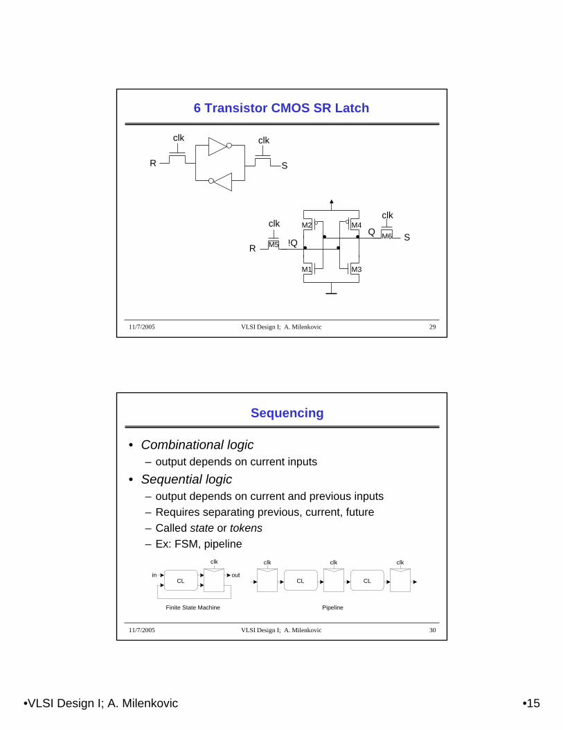
11/7/2005 VLSI Design I; A. Milenkovic 29
6 Transistor CMOS SR Latch
clkclk
SR
M1
SR
clk
!QQ
M2
M3
M4
M5M6
clk
11/7/2005 VLSI Design I; A. Milenkovic 30
Sequencing
• Combinational logic– output depends on current inputs
• Sequential logic– output depends on current and previous inputs– Requires separating previous, current, future– Called state or tokens– Ex: FSM, pipeline
CL
clk
in out
clk clk clk
CL CL
PipelineFinite State Machine
•VLSI Design I; A. Milenkovic •16
11/7/2005 VLSI Design I; A. Milenkovic 31
Sequencing Cont.
• If tokens moved through pipeline at constant speed, no sequencing elements would be necessary
• Ex: fiber-optic cable– Light pulses (tokens) are sent down cable– Next pulse sent before first reaches end of cable– No need for hardware to separate pulses– But dispersion sets min time between pulses
• This is called wave pipelining in circuits• In most circuits, dispersion is high
– Delay fast tokens so they don’t catch slow ones.
11/7/2005 VLSI Design I; A. Milenkovic 32
Sequencing Overhead
• Use flip-flops to delay fast tokens so they move through exactly one stage each cycle.
• Inevitably adds some delay to the slow tokens• Makes circuit slower than just the logic delay
– Called sequencing overhead• Some people call this clocking overhead
– But it applies to asynchronous circuits too– Inevitable side effect of maintaining sequence
•VLSI Design I; A. Milenkovic •17
11/7/2005 VLSI Design I; A. Milenkovic 33
Sequential Logic
CombinationalLogic
clock
Outputs
Sta
teR
egis
ters
NextState
CurrentState
Inputs
11/7/2005 VLSI Design I; A. Milenkovic 34
Timing Metrics
clock
In
Out
datastable
outputstable
outputstable
time
time
time
clock
D QIn Out
tsu thold
tc-q
•VLSI Design I; A. Milenkovic •18
11/7/2005 VLSI Design I; A. Milenkovic 35
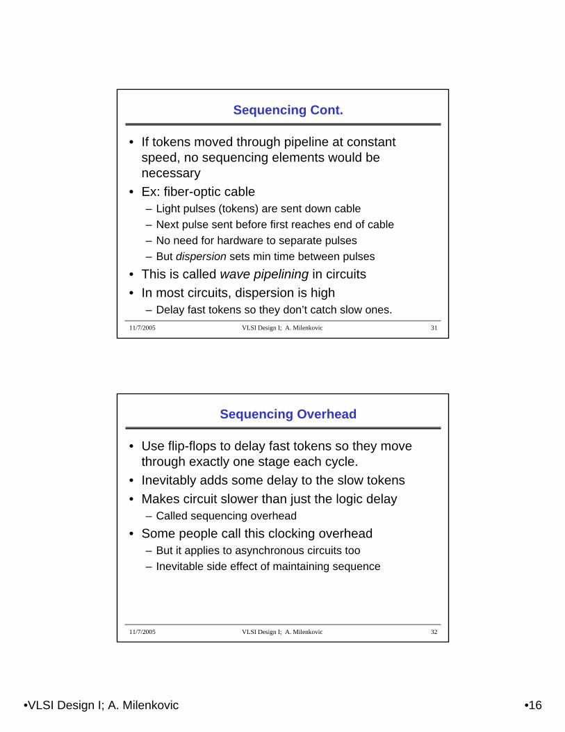
System Timing Constraints
CombinationalLogic
clock
Outputs
Sta
teR
egis
ters
NextState
CurrentState
Inputs
T ≥ tc-q + tplogic + tsutcdreg + tcdlogic ≥ thold
T (clock period)
11/7/2005 VLSI Design I; A. Milenkovic 36
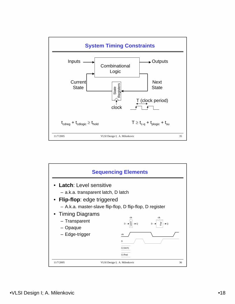
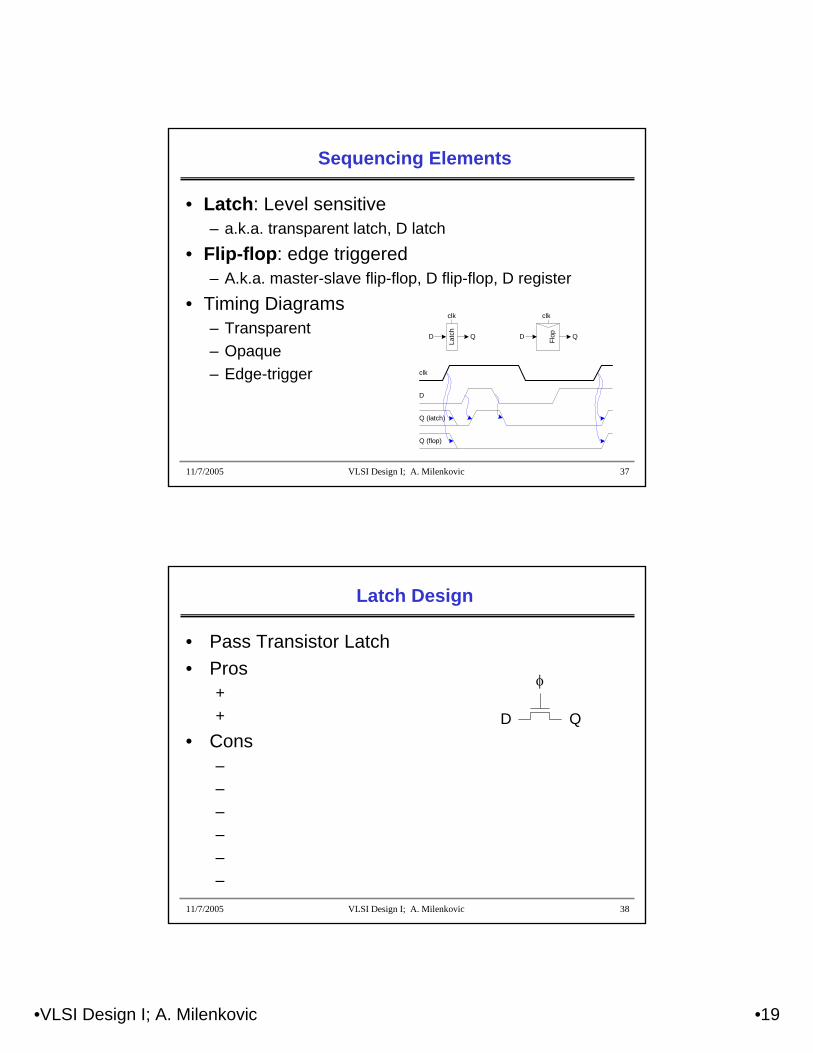
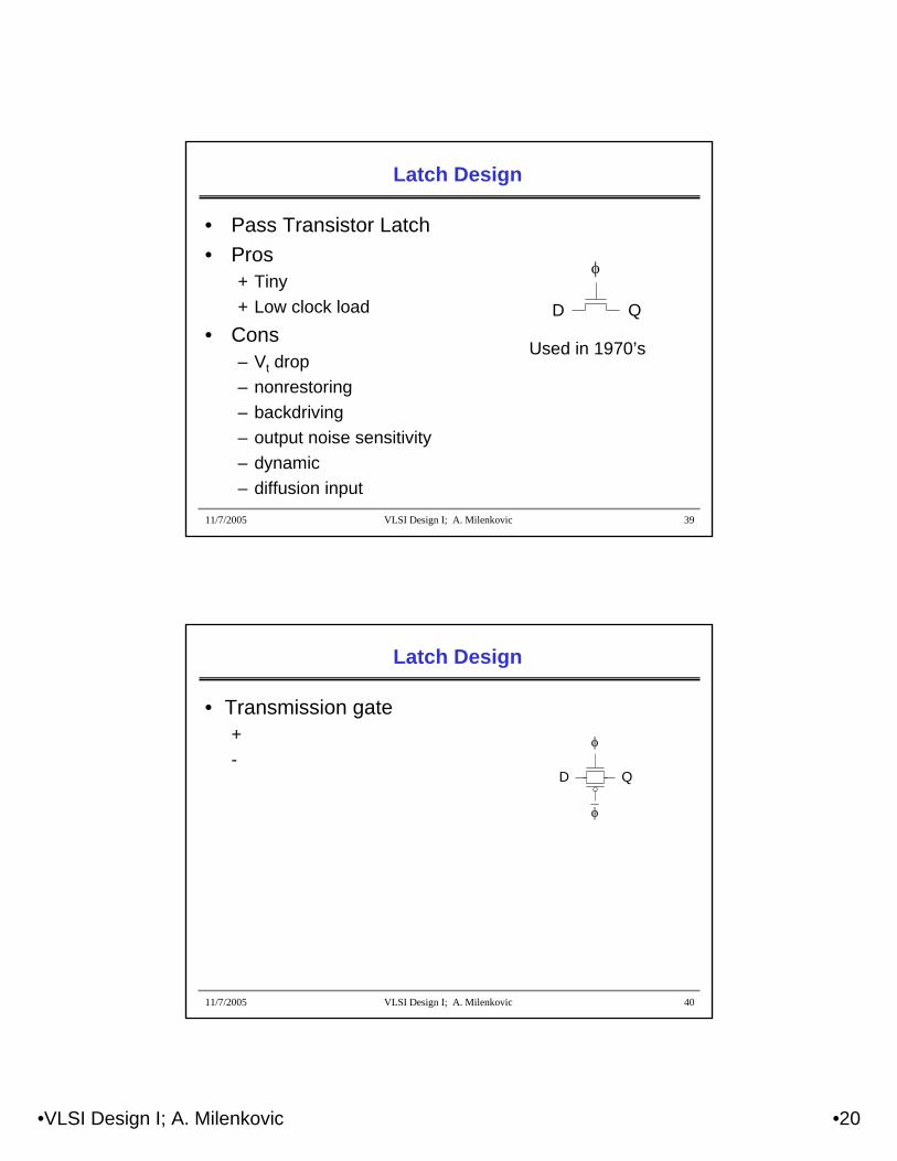
Sequencing Elements
• Latch: Level sensitive– a.k.a. transparent latch, D latch
• Flip-flop: edge triggered– A.k.a. master-slave flip-flop, D flip-flop, D register
• Flip-flop is built as pair of back-to-back latches
D Q
φ
φ
φ
φ
X
D
φ
φ
φ
φ
X
Q
Qφ
φ
φ
φ
•VLSI Design I; A. Milenkovic •27
11/7/2005 VLSI Design I; A. Milenkovic 53
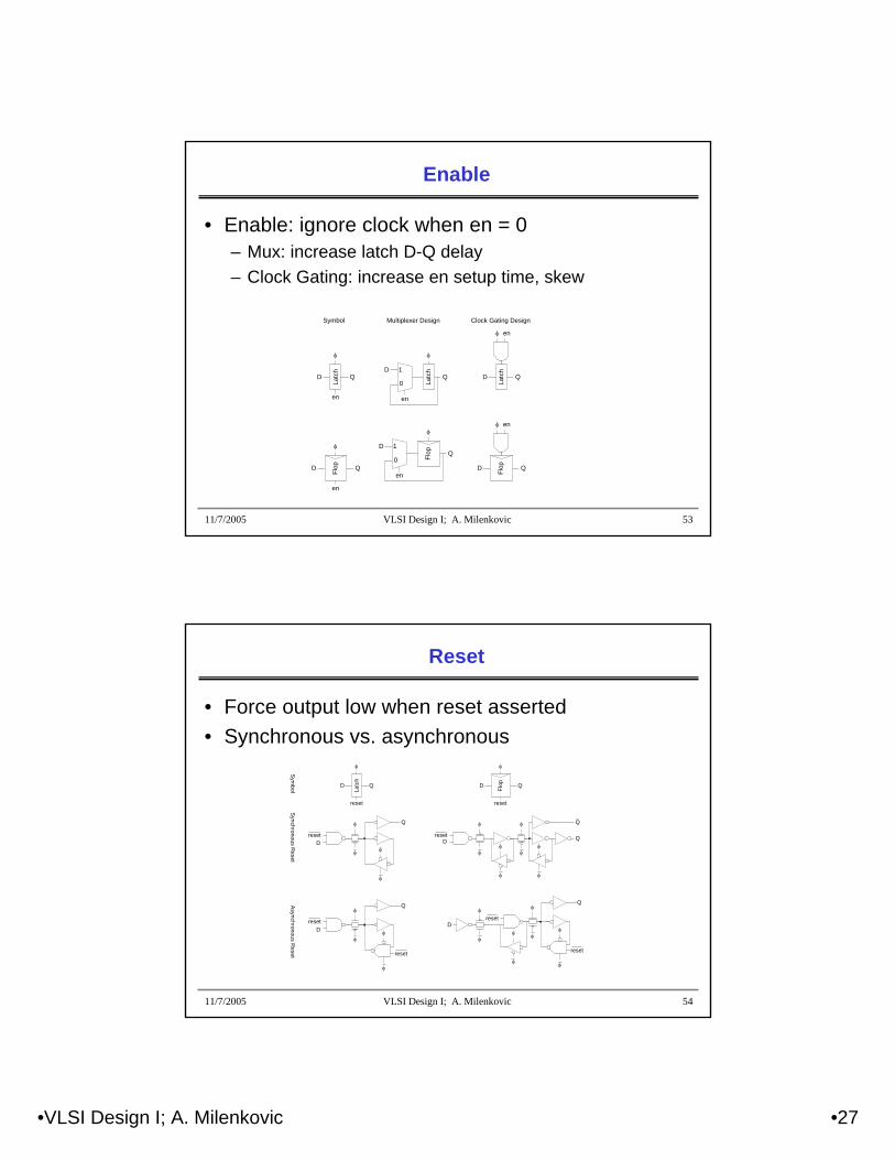
Enable
• Enable: ignore clock when en = 0– Mux: increase latch D-Q delay– Clock Gating: increase en setup time, skew
D Q
Latc
h
D Q
en
en
φ
φ
Latc
hDQ
φ
0
1
en
Latc
h
D Q
φ en
DQ
φ
0
1
enD Q
φ en
Flop
Flop
Flop
Symbol Multiplexer Design Clock Gating Design
11/7/2005 VLSI Design I; A. Milenkovic 54
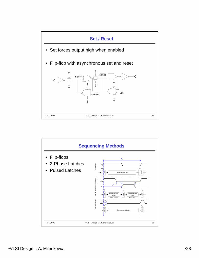
Reset
• Force output low when reset asserted• Synchronous vs. asynchronous
D
φ
φ
φ
φ
Q
Qφ
φ
φ
φ
reset
D
φ
φφ
φ
φ
φ
Qφ
φ
Dreset
φ
φ
Qφ
φ
Dreset
reset
φ
φ
reset
Synchronous R
esetA
synchronous Reset
Sym
bol FlopD Q
Latc
h
D Q
reset reset
φ φ
φ
φ
Q
reset
•VLSI Design I; A. Milenkovic •28
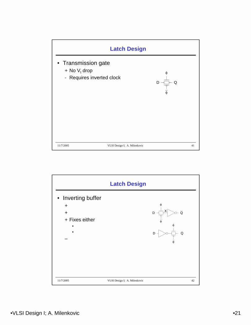
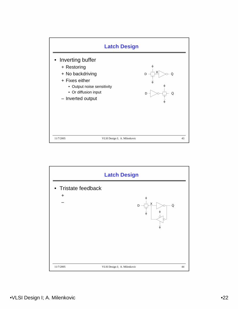
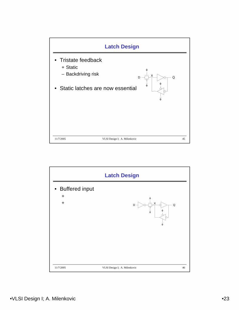
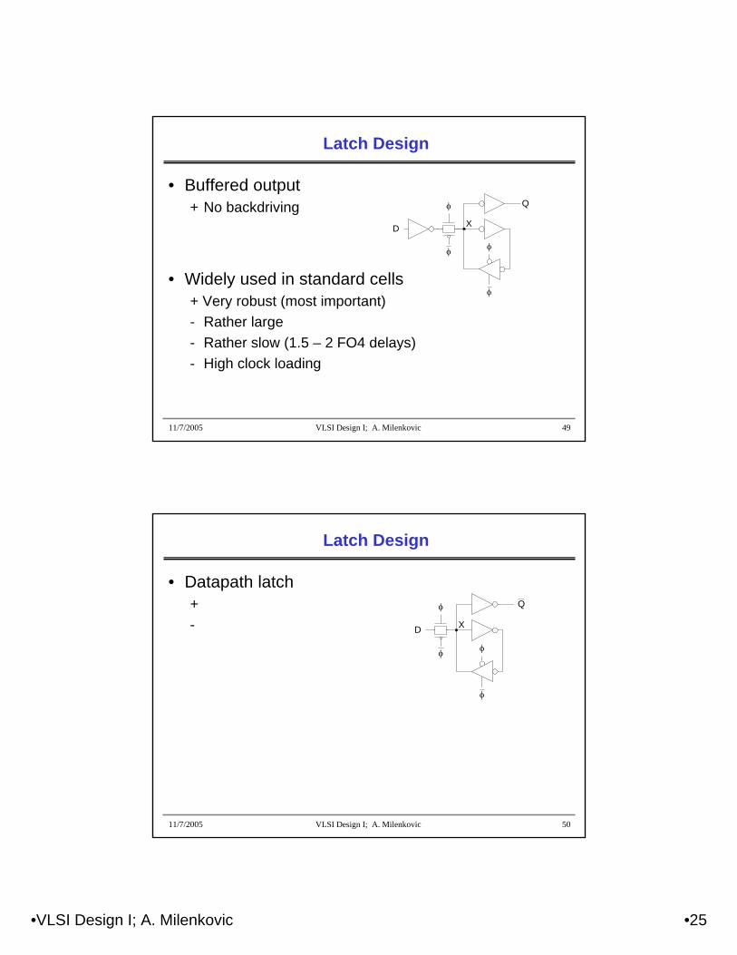
11/7/2005 VLSI Design I; A. Milenkovic 55
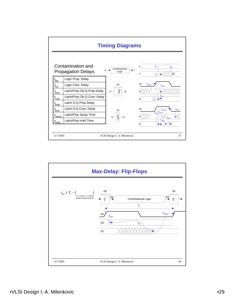
Set / Reset
• Set forces output high when enabled
• Flip-flop with asynchronous set and reset
D
φ
φ
φ
φφ
φ
Q
φ
φ
reset
set reset
set
11/7/2005 VLSI Design I; A. Milenkovic 56
Sequencing Methods
• Flip-flops• 2-Phase Latches• Pulsed Latches
Flip-FlopsFl
opLa
tch
Flop
clk
φ1
φ2
φp
clk clk
Latc
h
Latc
h
φp φp
φ1 φ1φ2
2-Phase Transparent Latches
Pulsed Latches
Combinational Logic
CombinationalLogic
CombinationalLogic
Combinational Logic
Latc
h
Latc
h
Tc
Tc/2
tnonoverlap tnonoverlap
tpw
Half-Cycle 1 Half-Cycle 1
•VLSI Design I; A. Milenkovic •29
11/7/2005 VLSI Design I; A. Milenkovic 57
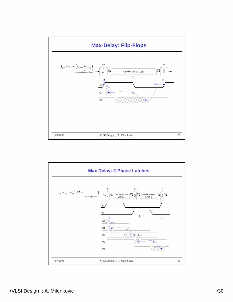
Timing Diagrams
Flop
A
Y
tpdCombinational
LogicA Y
D Q
clk clk
D
Q
Latc
hD Q
clk clk
D
Q
tcd
tsetup thold
tccq
tpcq
tccq
tsetup tholdtpcq
tpdqtcdqLatch/Flop Hold Timethold
Latch/Flop Setup Timetsetup
Latch D-Q Cont. Delaytpcq
Latch D-Q Prop Delaytpdq
Latch/Flop Clk-Q Cont. Delaytccq
Latch/Flop Clk-Q Prop Delaytpcq
Logic Cont. Delaytcd
Logic Prop. Delaytpd
Contamination and Propagation Delays
11/7/2005 VLSI Design I; A. Milenkovic 58
Max-Delay: Flip-Flops
F1 F2
clk
clk clk
Combinational Logic
Tc
Q1 D2
Q1
D2
tpd
tsetuptpcq
( )sequencing overhead
pd ct T≤ −1442443
•VLSI Design I; A. Milenkovic •30
11/7/2005 VLSI Design I; A. Milenkovic 59
Max-Delay: Flip-Flops
F1 F2
clk
clk clk
Combinational Logic
Tc
Q1 D2
Q1
D2
tpd
tsetuptpcq
( )setup
sequencing overhead
pd c pcqt T t t≤ − +14243
11/7/2005 VLSI Design I; A. Milenkovic 60
Max Delay: 2-Phase Latches
Tc
Q1
L1
φ1
φ2
L2 L3
φ1 φ1φ2
CombinationalLogic 1
CombinationalLogic 2
Q2 Q3D1 D2 D3
Q1
D2
Q2
D3
D1
tpd1
tpdq1
tpd2
tpdq2
( )1 2
sequencing overhead
pd pd pd ct t t T= + ≤ −1442443
•VLSI Design I; A. Milenkovic •31
11/7/2005 VLSI Design I; A. Milenkovic 61
Max Delay: 2-Phase Latches
Tc
Q1
L1
φ1
φ2
L2 L3
φ1 φ1φ2
CombinationalLogic 1
CombinationalLogic 2
Q2 Q3D1 D2 D3
Q1
D2
Q2
D3
D1
tpd1
tpdq1
tpd2
tpdq2
( )1 2
sequencing overhead
2pd pd pd c pdqt t t T t= + ≤ −123
11/7/2005 VLSI Design I; A. Milenkovic 62
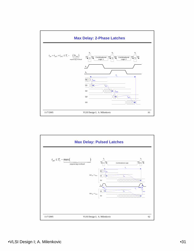
Max Delay: Pulsed Latches
Tc
Q1 Q2D1 D2
Q1
D2
D1
φp
φp φp
Combinational LogicL1 L2
tpw
(a) tpw > tsetup
Q1
D2
(b) tpw < tsetup
Tc
tpd
tpdq
tpcq
tpd tsetup
( )sequencing overhead
max pd ct T≤ −14444244443
•VLSI Design I; A. Milenkovic •32
11/7/2005 VLSI Design I; A. Milenkovic 63
Max Delay: Pulsed Latches
Tc
Q1 Q2D1 D2
Q1
D2
D1
φp
φp φp
Combinational LogicL1 L2
tpw
(a) tpw > tsetup
Q1
D2
(b) tpw < tsetup
Tc
tpd
tpdq
tpcq
tpd tsetup
( )setup
sequencing overhead
max ,pd c pdq pcq pwt T t t t t≤ − + −14444244443
11/7/2005 VLSI Design I; A. Milenkovic 64
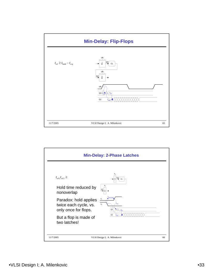
Min-Delay: Flip-Flops
cdt ≥ CL
clk
Q1
D2
F1
clk
Q1
F2
clk
D2
tcd
thold
tccq
•VLSI Design I; A. Milenkovic •33
11/7/2005 VLSI Design I; A. Milenkovic 65
Min-Delay: Flip-Flops
holdcd ccqt t t≥ − CL
clk
Q1
D2F1
clk
Q1
F2
clk
D2
tcd
thold
tccq
11/7/2005 VLSI Design I; A. Milenkovic 66
Min-Delay: 2-Phase Latches
1, 2 cd cdt t ≥CL
Q1
D2
D2
Q1
φ1
L1
φ2
L2
φ1
φ2
tnonoverlap
tcd
thold
tccq
Hold time reduced by nonoverlap
Paradox: hold applies twice each cycle, vs. only once for flops.
But a flop is made of two latches!
•VLSI Design I; A. Milenkovic •34
11/7/2005 VLSI Design I; A. Milenkovic 67
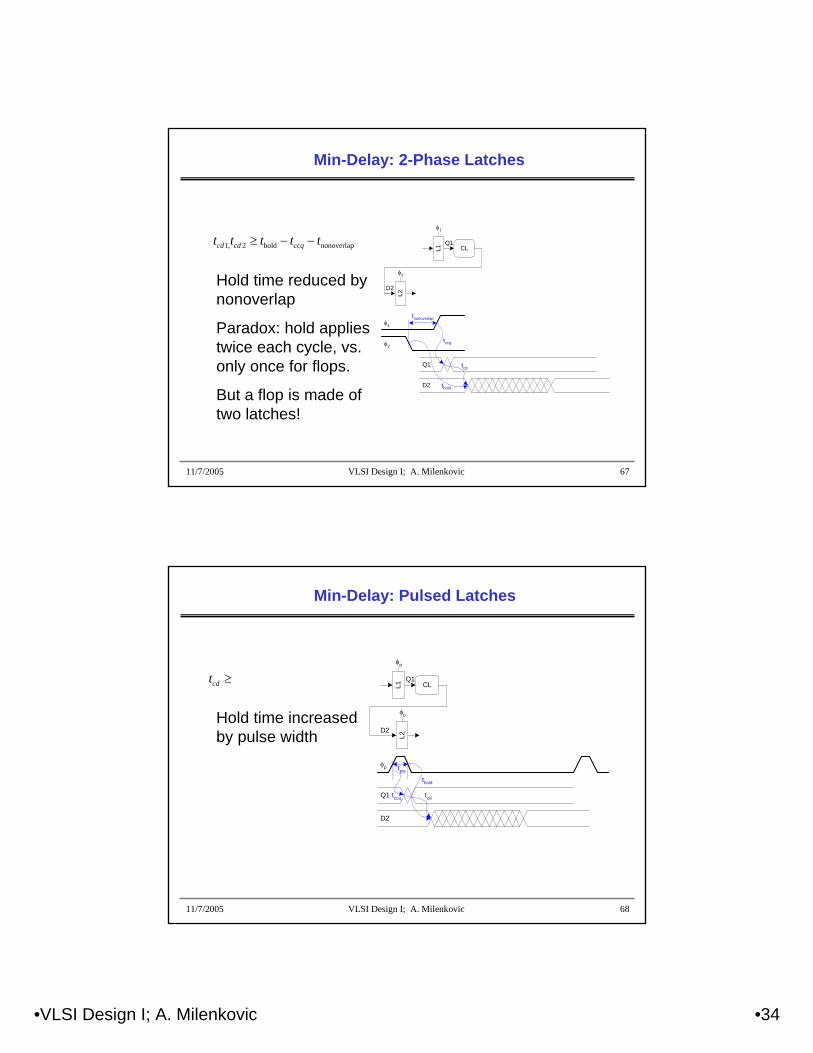
Min-Delay: 2-Phase Latches
1, 2 hold nonoverlapcd cd ccqt t t t t≥ − −CL
Q1
D2
D2
Q1
φ1
L1
φ2
L2
φ1
φ2
tnonoverlap
tcd
thold
tccq
Hold time reduced by nonoverlap
Paradox: hold applies twice each cycle, vs. only once for flops.
But a flop is made of two latches!
11/7/2005 VLSI Design I; A. Milenkovic 68
Min-Delay: Pulsed Latches
cdt ≥CL
Q1
D2
Q1
D2
φp tpw
φp
L1
φp
L2
tcd
thold
tccq
Hold time increased by pulse width
•VLSI Design I; A. Milenkovic •35
11/7/2005 VLSI Design I; A. Milenkovic 69
Min-Delay: Pulsed Latches
holdcd ccq pwt t t t≥ − +CL
Q1
D2
Q1
D2
φp tpw
φp
L1
φp
L2
tcd
thold
tccq
Hold time increased by pulse width
11/7/2005 VLSI Design I; A. Milenkovic 70
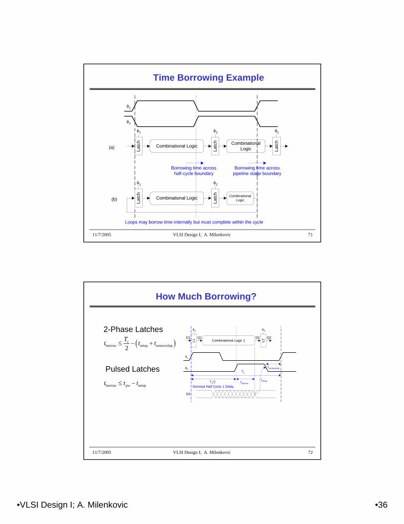
Time Borrowing
• In a flop-based system:– Data launches on one rising edge– Must setup before next rising edge– If it arrives late, system fails– If it arrives early, time is wasted– Flops have hard edges
• In a latch-based system– Data can pass through latch while transparent– Long cycle of logic can borrow time into next– As long as each loop completes in one cycle
•VLSI Design I; A. Milenkovic •36
11/7/2005 VLSI Design I; A. Milenkovic 71
Time Borrowing Example
Latc
h
Latc
h
Latc
h
Combinational Logic CombinationalLogic
Borrowing time acrosshalf-cycle boundary
Borrowing time acrosspipeline stage boundary
(a)
(b) Latc
h
Latc
h
Combinational Logic CombinationalLogic
Loops may borrow time internally but must complete within the cycle
φ1
φ2
φ1 φ1
φ1
φ2
φ2
11/7/2005 VLSI Design I; A. Milenkovic 72
How Much Borrowing?
Q1
L1
φ1
φ2
L2
φ1 φ2
Combinational Logic 1Q2D1 D2
D2
Tc
Tc/2 Nominal Half-Cycle 1 Delay
tborrow
tnonoverlap
tsetup
( )borrow setup nonoverlap2cTt t t≤ − +
2-Phase Latches
borrow setuppwt t t≤ −
Pulsed Latches
•VLSI Design I; A. Milenkovic •37
11/7/2005 VLSI Design I; A. Milenkovic 73
Clock Skew
• We have assumed zero clock skew• Clocks really have uncertainty in arrival time
– Decreases maximum propagation delay– Increases minimum contamination delay– Decreases time borrowing
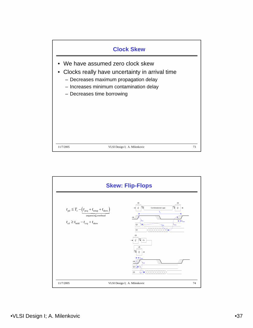
11/7/2005 VLSI Design I; A. Milenkovic 74
Skew: Flip-Flops
F1 F2
clk
clk clk
Combinational Logic
Tc
Q1 D2
Q1
D2
tskew
CL
Q1
D2
F1
clk
Q1
F2
clk
D2
clk
tskew
tsetup
tpcq
tpdq
tcd
thold
tccq
( )setup skew
sequencing overhead
hold skew
pd c pcq
cd ccq
t T t t t
t t t t
≤ − + +
≥ − +
144424443
•VLSI Design I; A. Milenkovic •38
11/7/2005 VLSI Design I; A. Milenkovic 75
Skew: Latches
Q1
L1
φ1
φ2
L2 L3
φ1 φ1φ2
CombinationalLogic 1
CombinationalLogic 2
Q2 Q3D1 D2 D3
( )
( )
sequencing overhead
1 2 hold nonoverlap skew
borrow setup nonoverlap skew
2
,
2
pd c pdq
cd cd ccq
c
t T t
t t t t t t
Tt t t t
≤ −
≥ − − +
≤ − + +
123
2-Phase Latches
( )
( )
setup skew
sequencing overhead
hold skew
borrow setup skew
max ,pd c pdq pcq pw
cd pw ccq
pw
t T t t t t t
t t t t t
t t t t
≤ − + − +
≥ + − +
≤ − +
1444442444443
Pulsed Latches
11/7/2005 VLSI Design I; A. Milenkovic 76
Two-Phase Clocking
• If setup times are violated, reduce clock speed• If hold times are violated, chip fails at any speed• In this class, working chips are most important
– No tools to analyze clock skew• An easy way to guarantee hold times is to use 2-
phase latches with big nonoverlap times• Call these clocks φ1, φ2 (ph1, ph2)
•VLSI Design I; A. Milenkovic •39
11/7/2005 VLSI Design I; A. Milenkovic 77
Safe Flip-Flop
• In class, use flip-flop with nonoverlapping clocks– Very slow – nonoverlap adds to setup time– But no hold times
• In industry, use a better timing analyzer– Add buffers to slow signals if hold time is at risk
D
φ2
X
Q
Q
φ1
φ2
φ1
φ1φ1
φ2
φ2
11/7/2005 VLSI Design I; A. Milenkovic 78
Summary
• Flip-Flops:– Very easy to use, supported by all tools
• 2-Phase Transparent Latches:– Lots of skew tolerance and time borrowing
• Pulsed Latches:– Fast, some skew tol & borrow, hold time risk