CS 150 - Fall 2005 – Lec #14: Control Implementation - 1 Controller Implementation-- Part I • Alternative controller FSM implementation approaches based on: – Classical Moore and Mealy machines – Time state: Divide and Counter – Jump counters – Microprogramming (ROM) based approaches » branch sequencers » horizontal microcode » vertical microcode
Transcript
CS 150 - Fall 2005 – Lec #14: Control Implementation - 1
Controller Implementation--Part I
• Alternative controller FSM implementation approaches based on:– Classical Moore and Mealy machines– Time state: Divide and Counter– Jump counters– Microprogramming (ROM) based approaches
CS 150 - Fall 2005 – Lec #14: Control Implementation - 2
IN
Q0
Q1
CLK
100
Cascading Edge-triggered Flip-Flops
• Shift register– New value goes into first stage– While previous value of first stage goes into second stage– Consider setup/hold/propagation delays (prop must be > hold)
CLK
INQ0 Q1
D Q D Q OUT
CS 150 - Fall 2005 – Lec #14: Control Implementation - 3
IN
Q0
Q1
CLK
100
Cascading Edge-triggered Flip-Flops
• Shift register– New value goes into first stage– While previous value of first stage goes into second stage– Consider setup/hold/propagation delays (prop must be > hold)
CLK
INQ0 Q1
D Q D Q OUT
DelayClk1
Clk1
CS 150 - Fall 2005 – Lec #14: Control Implementation - 4
original state: IN = 0, Q0 = 1, Q1 = 1due to skew, next state becomes: Q0 = 0, Q1 = 0, and not Q0 = 0, Q1 = 1
CLK1 is a delayedversion of CLK
In
Q0
Q1
CLK
CLK1
100
Clock Skew
• The problem– Correct behavior assumes next state of all storage elements
determined by all storage elements at the same time– Difficult in high-performance systems because time for clock to
arrive at flip-flop is comparable to delays through logic (and will soon become greater than logic delay)
– Effect of skew on cascaded flip-flops:
CS 150 - Fall 2005 – Lec #14: Control Implementation - 5
Why Gating of Clocks is Bad!
Reg
Clk
LD
Reg
ClkLD
GOOD BAD
Do NOT Mess With Clock Signals!
gatedClK
CS 150 - Fall 2005 – Lec #14: Control Implementation - 6
Why Gating of Clocks is Bad!
Do NOT Mess With Clock Signals!
Clk
LD
gatedClk
LD generated by FSMshortly after rising edge of CLK
Runt pulse plays HAVOC with register internals!
Clk
LDn
gatedClk
NASTY HACK: delay LD throughnegative edge triggered FF toensure that it won’t change duringnext positive edge event
Clk skew PLUS LD delayed by half clock cycle …What is the effect on your register transfers?
CS 150 - Fall 2005 – Lec #14: Control Implementation - 7
Why Gating of Clocks is Bad!
Clk
Reset
Reg
Cou
nte
r
BAD
Do NOT Mess With Clock Signals!
slowClK
CS 150 - Fall 2005 – Lec #14: Control Implementation - 8
Why Gating of Clocks is Bad!
Clk
Reset
Reg
Cou
nte
r
Better!
Do NOT Mess With Clock Signals!
LD
CS 150 - Fall 2005 – Lec #14: Control Implementation - 9
Alternative Ways to Implement Processor FSMs• "Random Logic" based on Moore and Mealy Design
– Classical Finite State Machine Design
• Divide and Conquer Approach: Time-State Method– Partition FSM into multiple communicating FSMs
• Microprogramming: ROM-based methods– Direct encoding of next states and outputs
CS 150 - Fall 2005 – Lec #14: Control Implementation - 10
Random Logic
• Perhaps poor choice of terms for "classical" FSMs
• Contrast with structured logic: PLA, FPGA, ROM-based (latter used in microprogrammed controllers)
• Could just as easily construct Moore and Mealy machines with these components
CS 150 - Fall 2005 – Lec #14: Control Implementation - 11
Moore MachineState Diagram
Note capture of MBRin these states
0 PC
Reset
Wait/
Wait/
Wait/
Wait/
Wait/
Wait/
=11=10
=0=1
BR0
BR1
IF3
OD
=00 =01
AD0ST0
ST1 AD1
Wait/Wait/
AD2
Wait/Wait/
LD0
LD1
LD2
Wait/
Wait/
PC MAR, PC + 1 PC
MAR Mem, 1 Read/Write,
1 Request, Mem MBR
MBR IR
IR MAR IR MAR
IR PC
MAR Mem,
1 Read/Write,
1 Request,
Mem MBR
MAR Mem,
0 Read/Write,
1 Request,
MBR Mem
MAR Mem,
1 Read/Write,
1 Request,
Mem MBR
MBR AC MBR + AC AC
IF2
IF1
IF0
RES
IR MAR,
AC MBR
CS 150 - Fall 2005 – Lec #14: Control Implementation - 12
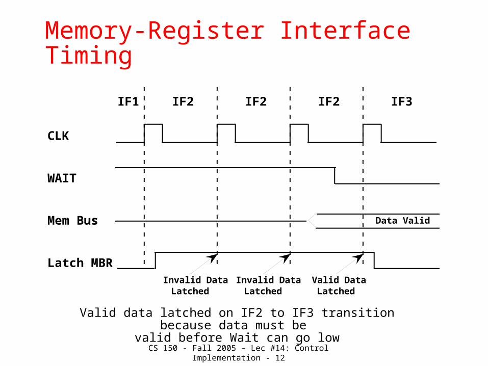
Memory-Register Interface Timing
Valid data latched on IF2 to IF3 transitionbecause data must be
valid before Wait can go low
CLK WAIT Mem Bus Latch MBR
IF1 IF2 IF2 IF2 IF3
Invalid Data Latched
Invalid Data Latched
Valid Data Latched
Data Valid
CS 150 - Fall 2005 – Lec #14: Control Implementation - 13
Moore Machine Diagram
16 states, 4 bit state register
Next State Logic: 9 Inputs, 4 Outputs
Output Logic: 4 Inputs, 18 Outputs
These can be implemented via ROM or PAL/PLA
Next State: 512 x 4 bit ROMOutput: 16 x 18 bit ROM
Next State Logic
Clock State
Reset Wait IR<15> IR<14> AC<15>
Output Logic
Read/Write Request 0 → PC
+ 1 PC
→ PC
PC→ ABUS
IR→ ABUS
ABUS
→ MAR
ABUS
→ PC
MAR
→ Memory Address Bus
Memory Data Bus
→ MBR
MBR
→ Memory Data Bus
MBR
→ MBUS
MBUS
→ IR
MBUS
→ ALU B
MBUS
→ AC
RBUS
→ AC
RBUS
→ MBR
ALU ADD
CS 150 - Fall 2005 – Lec #14: Control Implementation - 14
Moore Machine State Table
Reset WaitIR<15>IR<14>AC<15>Current StateNext State Register Transfer Ops
1 X X X X X RES (0000)
0 X X X X RES (0000) IF0 (0001) 0 PC
0 X X X X IF0 (0001) IF1 (0001) PC MAR, PC + 1 PC
0 0 X X X IF1 (0010) IF1 (0010)
0 1 X X X IF1 (0010) IF2 (0011)
0 1 X X X IF2 (0011) IF2 (0011) MAR Mem, Read,
0 0 X X X IF2 (0011) IF3 (0100) Request, Mem MBR
0 0 X X X IF3 (0100) IF3 (0100) MBR IR
0 1 X X X IF3 (0100) OD (0101)
0 X 0 0 X OD (0101) LD0 (0110)
0 X 0 1 X OD (0101) ST0 (1001)
0 X 1 0 X OD (0101) AD0 (1011)
0 X 1 1 X OD (0101) BR0 (1110)
CS 150 - Fall 2005 – Lec #14: Control Implementation - 15
Reset WaitIR<15>IR<14>AC<15> Current State Next State Register Transfer Ops
0 X X X X LD0 (0110) LD1 (0111) IR MAR
0 1 X X X LD1 (0111) LD1 (0111) MAR Mem, Read,
0 0 X X X LD1 (0111) LD2 (1000) Request, Mem MBR
0 X X X X LD2 (1000) IF0 (0001) MBR AC
0 X X X X ST0 (1001) ST1 (1010) IR MAR, AC MBR
0 1 X X X ST1 (1010) ST1 (1010) MAR Mem, Write,
0 0 X X X ST1 (1010) IF0 (0001) Request, MBR Mem
0 X X X X AD0 (1011) AD1 (1100) IR MAR
0 1 X X X AD1 (1100) AD1 (1100) MAR Mem, Read,
0 0 X X X AD1 (1100) AD2 (1101) Request, Mem MBR
0 X X X X AD2 (1101) IF0 (0001) MBR + AC AC
0 X X X 0 BR0 (1110) IF0 (0001)
0 X X X 1 BR0 (1110) BR1 (1111)
0 X X X X BR1 (1111) IF0 (0001) IR PC
Moore Machine State Table
CS 150 - Fall 2005 – Lec #14: Control Implementation - 16
Moore Machine State Transition Table
• Observations:– Extensive use of Don't Cares– Inputs used only in a small number of state
e.g., AC<15> examined only in BR0 state IR<15:14> examined only in OD state
• Some outputs always asserted in a group• ROM-based implementations cannot take
advantage of don't cares• However, ROM-based implementation can skip
state assignment step
CS 150 - Fall 2005 – Lec #14: Control Implementation - 19
SynchronizerCircuitry atInputs and
Outputs
SynchronizerCircuitry atInputs and
OutputsOutput Logic
Output Logic
Output Logic
D
D
D
D
STATE STATE STATE
Q Q
Q
A A
A' A'
Q
ƒ
ƒ' ƒ
ƒ
ƒ'
A
Synchronous Mealy Machines• Standard Mealy Machine has asynchronous outputs• Change in response to input changes, independent of clock• Revise Mealy Machine design so outputs change only on clock
edges• One approach: non-overlapping clocks
CS 150 - Fall 2005 – Lec #14: Control Implementation - 20
Synchronous Mealy Machines
Case I: Synchronizers at Inputs and Outputs
A asserted in Cycle 0, ƒ becomes asserted after 2 cycle delay!
This is clearly overkill!
cycle 0 cycle 1 cycle 2
CLK
A
A'
ƒ
ƒ'
S0
S1
S2
A/ƒ
CS 150 - Fall 2005 – Lec #14: Control Implementation - 21
Synchronous Mealy Machine
Case II: Synchronizers on Inputs
A asserted in Cycle 0, ƒ follows in next cycle
Same as using delayed signal (A') in Cycle 1!
cycle 0 cycle 1 cycle 2
CLK
A
A'
ƒ
S0
S1
A/ƒ
S0
S1
A'/ƒ
CS 150 - Fall 2005 – Lec #14: Control Implementation - 22
Synchronous Mealy Machines
Case III: Synchronized Outputs
A asserted during Cycle 0, ƒ' asserted in next cycle
Effect of ƒ delayed one cycle
cycle 0 cycle 1 cycle 2
CLK
A
ƒ
ƒ'
S0
S1
A/ƒ
CS 150 - Fall 2005 – Lec #14: Control Implementation - 23
– Latter two already come from registers, and are sync'd to clock
– Possible to load IR with new instruction in one state & perform multiway branch on opcode in next state
– Best solution for Reset and Wait: synchronized inputs» Place D flipflops between these external signals and the» control inputs to the processor FSM» Sync'd versions of Reset and Wait delayed by one clock
cycle
CS 150 - Fall 2005 – Lec #14: Control Implementation - 24
CS 150 - Fall 2005 – Lec #14: Control Implementation - 34
Jump Counter
CLR, CNT, LDimplemented via Mux Logic
Active Lo outputs:hi input inverted at
the output
Note that CNT isactive hi on counter
so invert MUX inputs!
CLR = CLRm + Reset
CLR = CLRm + Reset/CLR
+
+ +
163
154
150150150
/CLRm/Reset /CLR
CNT
Jump State
IR<15>
IR14
IR15
IR<14>
3 2 1 0
P T
CLKD C B A
RCO
QD QC QB QA
LOAD
CLR
/LDReset
Wait
/Reset
/Wait
1 0
1 0
G2 G1
D C B A
Wait/Wait
EOUT EOUT EOUT
/Wait
CNT
10
/CLRm /LD
151413121110
9876543210
\S13\S12\S11\S10\S9\S8\S7\S6\S5\S4\S3\S2\S1\S0
E15E14E13E12E11E10E9E8E7E6E5E4E3E2E1E0
G
S3 S2 S1 S0
E15E14E13E12E11E10E9E8E7E6E5E4E3E2E1E0
G
S3 S2 S1 S0
E15E14E13E12E11E10E9E8E7E6E5E4E3E2E1E0
G
S3 S2 S1 S0
CS 150 - Fall 2005 – Lec #14: Control Implementation - 35
Jump CountersMicrooperation implementation 0 PC = Reset PC + 1 PC = S0 PC MAR = S0 MAR Memory Address Bus = Wait•(S1 + S2 + S5 + S6 + S8 + S9 + S11 + S12) Memory Data Bus MBR = Wait•(S2 + S6 + S11) MBR Memory Data Bus = Wait•(S8 + S9) MBR IR = Wait•S3 MBR AC = Wait•S7 AC MBR = IR15•IR14•S4 AC + MBR AC = Wait•S12 IR<13:0> MAR = (IR15•IR14 + IR15•IR14 + IR15•IR14)•S4 IR<13:0> PC = AC15•S13 1 Read/Write = Wait•(S1 + S2 + S5 + S6 + S11 + S12) 0 Read/Write = Wait•(S8 + S9) 1 Request = Wait•(S1 + S2 + S5 + S6 + S8 + S9 + S11 + S12)
Jump Counters: CNT, CLR, LD function of current state + WaitWhy not store these as outputs of the Jump State ROM?Make Wait and Current State part of ROM address32 x as many words, 7 bits wide
CS 150 - Fall 2005 – Lec #14: Control Implementation - 36
Controller Implementation Summary(Part I!)• Control Unit Organization
– Register transfer operation– Classical Moore and Mealy machines– Time State Approach– Jump Counter– Next Time:
» Branch Sequencers» Horizontal and Vertical Microprogramming