28
CSE 140 Lecture 8 Sequential Networks Professor CK Cheng CSE Dept. UC San Diego 1
| Date post: | 19-Dec-2015 |
| Category: |
Documents |
| View: | 218 times |
| Download: | 3 times |

CSE 140 Lecture 8Sequential Networks
Professor CK Cheng
CSE Dept.
UC San Diego
1

Part II. Sequential Networks (Ch. 3)
Memory / Time steps
Clock
Memory: Flip flopsSpecification: Finite State MachinesImplementation: Excitation Tables
xi yi
si
yi=fi(St,X)si
t+1=gi(St,X)
2

Memory Devices
• Memory Storage
• Latches
• Flip-Flops– SR, D, T, JK– State Tables– Characteristic Expressions
3

Memory Storage: Capacitive Loads
• Fundamental building block of other state elements• Two outputs: Q, Q• No inputs
QQQ
Q
I1
I2
I2 I1
4

Capacitive Loads
Q
Q
I1
I2
0
1
1
0
• Consider the two possible cases:– Q = 0: then Q’ = 1 and Q = 0 (consistent)
– Q = 1: then Q’ = 0 and Q = 1 (consistent)
– Bistable circuit stores 1 bit of state in the state variable, Q (or Q’ )
• But there are no inputs to control the state
Q
Q
I1
I2
1
0
0
1
5

SR (Set/Reset) Latch
R
S
Q
Q
N1
N2
• SR Latch
• Consider the four possible cases:– S = 1, R = 0
– S = 0, R = 1
– S = 0, R = 0
– S = 1, R = 1
6

SR Latch Analysis– S = 1, R = 0: then Q = 1 and Q = 0
– S = 0, R = 1: then Q = 0 and Q = 1
R
S
Q
Q
N1
N2
0
1
R
S
Q
Q
N1
N2
1
0
7

SR Latch Analysis– S = 1, R = 0: then Q = 1 and Q = 0
– S = 0, R = 1: then Q = 0 and Q = 1
R
S
Q
Q
N1
N2
0
1
1
01
0
R
S
Q
Q
N1
N2
1
0
0
10
1
8

SR Latch Analysis– S = 0, R = 0: then Q = Qprev
– S = 1, R = 1: then Q = 0 and Q = 0
R
S
Q
Q
N1
N2
1
1
R
S
Q
Q
N1
N2
0
0
R
S
Q
Q
N1
N2
0
0
0
Qprev = 0 Qprev = 1
9

S
R
y
QQ = (R+y)’
y = (S+Q)’
10

Flip-flop Components
S
R
SR F-F (Set-Reset)
Inputs: S, R State: (Q, y)
y
Q
11

Id Q y S R Q* y Q** y** Q*** y***
0 0 0 0 0 1 1 0 0 1 1
1 0 0 0 1 0 1 0 1 0 12 0 0 1 0 1 0 1 0 1 03 0 0 1 1 0 0 0 0 0 04 0 1 0 0 0 1 0 1 0 15 0 1 0 1 0 1 0 1 0 16 0 1 1 0 0 0 1 0 1 07 0 1 1 1 0 0 0 0 0 08 1 0 0 0 1 0 1 0 1 09 1 0 0 1 0 0 0 1 0 110 1 0 1 0 1 0 1 0 1 011 1 0 1 1 0 0 0 0 0 012 1 1 0 0 0 0 1 1 0 013 1 1 0 1 0 0 0 1 0 114 1 1 1 0 0 0 1 0 1 015 1 1 1 1 0 0 0 0 0 0
Q y
State
TransitionSR
1010
00
11
00
10SR
1110
01 11
0111
01
10 0010
0001
0011
State Diagram
01
12

CASES:SR=01, (Q,y) = (0,1)SR=10, (Q,y) = (1,0)SR=11, (Q,y) = (0,0)SR = 00 => if (Q,y) = (0,0) or (1,1), the output keeps changingSolutions: 1) SR = (0,0), or
2) SR = (1,1).
0 0 0 1 -1 1 0 1 -
PSinputs
00 01 10 11
State table
Q(t+1)
SR
Characteristic ExpressionQ(t+1) = S(t)+R’(t)Q(t)
NS (next state)
Q(t)
13

SR Latch Analysis– S = 0, R = 0: then Q = Qprev and Q = Qprev
(memory!)
– S = 1, R = 1: then Q = 0 and Q = 0 (invalid state: Q ≠ NOT Q)
R
S
Q
Q
N1
N2
1
1
0
00
0
R
S
Q
Q
N1
N2
0
0
1
01
0
R
S
Q
Q
N1
N2
0
0
0
10
1
Qprev = 0 Qprev = 1
14

SR Latch Symbol• SR stands for Set/Reset Latch
– Stores one bit of state (Q)
• Control what value is being stored with S, R inputs– Set: Make the output 1 (S = 1, R = 0, Q = 1)
– Reset: Make the output 0 (S = 0, R = 1, Q = 0)
• Must do something to avoid
invalid state (when S = R = 1)
S
R Q
Q
SR LatchSymbol
15

D Latch
D LatchSymbol
CLK
D Q
Q
• Two inputs: CLK, D– CLK: controls when the output changes
– D (the data input): controls what the output changes to
• Function– When CLK = 1, D passes through to Q
(the latch is transparent)
– When CLK = 0, Q holds its previous value (the latch is opaque)
• Avoids invalid case when Q ≠ NOT Q
16

D Latch Internal Circuit
S
R Q
Q
Q
QD
CLKD
R
S
CLK
D Q
Q
S R Q QCLK D
0 X1 01 1
D
17
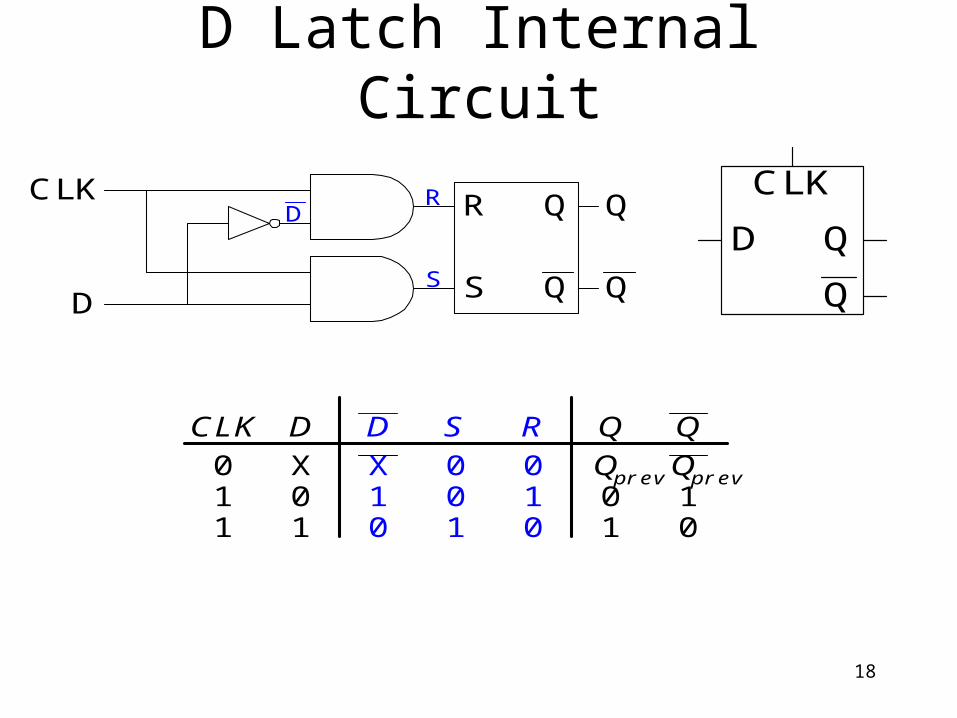
D Latch Internal Circuit
S
R Q
Q
Q
QD
CLKD
R
S
CLK
D Q
Q
S R Q
0 0 Qprev0 1 01 0 1
Q
10
CLK D
0 X1 01 1
D
X10
Qprev
18

D Flip-Flop• Two inputs: CLK, D• Function
– The flip-flop “samples” D on the rising edge of CLK
• When CLK rises from 0 to 1, D passes through to Q
• Otherwise, Q holds its previous value
– Q changes only on the rising edge of CLK
• A flip-flop is called an edge-triggered device because it is activated on the clock edge
D Flip-FlopSymbols
D Q
Q
19

D Flip-Flop Internal Circuit
CLK
D Q
Q
CLK
D Q
Q
Q
Q
DN1
CLK
L1 L2
• Two back-to-back latches (L1 and L2) controlled by complementary clocks
• When CLK = 0– L1 is transparent, L2 is opaque
– D passes through to N1
• When CLK = 1– L2 is transparent, L1 is opaque
– N1 passes through to Q
• Thus, on the edge of the clock (when CLK rises from 0 1)– D passes through to Q
CLK
D Q
Q
CLK
D Q
Q
Q
Q
DN1
CLK
L1 L2
20

D Flip-Flop vs. D LatchCLK
D Q
Q
D Q
Q
CLK
D
Q (latch)
Q (flop)
21

D Flip-Flop vs. D LatchCLK
D Q
Q
D Q
Q
CLK
D
Q (latch)
Q (flop)
22

Latch and Flip-flops (two latches)
Latch can be considered as a door
CLK = 0, door is shut CLK = 1, door is unlocked
A flip-flop is a two door entrance
CLK = 1 CLK = 0 CLK = 1 23

D Flip-Flop (Delay)
D
CLK
Q
Q’
Id D Q(t) Q(t+1)
0 0 0 0
1 0 1 0
2 1 0 1
3 1 1 1
Characteristic ExpressionQ(t+1) = D(t)
0 0 11 0 1
PS D 0 1
State table
NS= Q(t+1)24

JK F-F
J
CLK
Q
Q’ 0 0 0 1 ?1 1 0 1 ?
PSJK
00 01 10 11
State table
Q(t+1)
K
25

JK F-F
J
CLK
Q
Q’
Characteristic ExpressionQ(t+1) = Q(t)K’(t)+Q’(t)J(t)
0 0 0 1 11 1 0 1 0
PSJK
00 01 10 11
State table
Q(t+1)
K
26

T
CLK
Q
Q’
Characteristic Expression Q(t+1) = Q’(t)T(t) + Q(t)T’(t)
0 0 11 1 0
PS T 0 1
State table
Q(t+1)
T Flip-Flop (Toggle)
27

Using a JK F-F to implement a D and T F-F
J
K
Q
Q’
DCLK
D flip flop
J
K
Q
Q’
TCLK
T flip flop28


