Processor vs DRAM speed disparity continues to grow
0.01
0.1
1
10
100
1000
VAX/1980 PPro/1996 2010+
Core
Memory
Clo
cks
pe
r in
stru
ctio
n
Clo
cks
pe
r D
RA
M a
cces
s
Good memory hierarchy (cache) design is increasingly important to overall performance
CSE431 Chapter 5A.5 Irwin, PSU, 2008
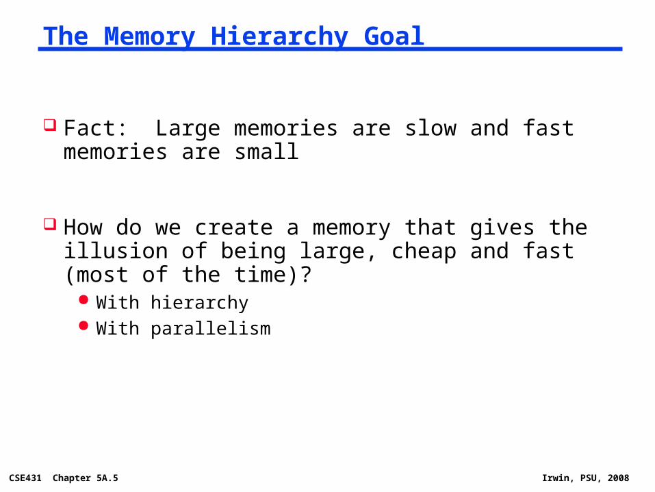
The Memory Hierarchy Goal
Fact: Large memories are slow and fast memories are small
How do we create a memory that gives the illusion of being large, cheap and fast (most of the time)?
With hierarchy With parallelism
CSE431 Chapter 5A.6 Irwin, PSU, 2008
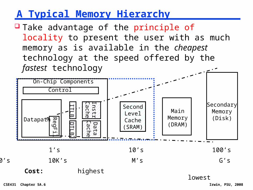
SecondLevelCache
(SRAM)
A Typical Memory Hierarchy
Control
Datapath
SecondaryMemory(Disk)
On-Chip Components
RegF
ile
MainMemory(DRAM)
Data
Cache
InstrC
ache
ITLB
DT
LB
Speed (%cycles): ½’s 1’s 10’s 100’s 10,000’s
Size (bytes): 100’s 10K’s M’s G’s T’s
Cost: highest lowest
Take advantage of the principle of locality to present the user with as much memory as is available in the cheapest technology at the speed offered by the fastest technology
CSE431 Chapter 5A.7 Irwin, PSU, 2008
Memory Hierarchy Technologies Caches use SRAM for speed and technology
compatibility Fast (typical access times of 0.5 to 2.5 nsec) Low density (6 transistor cells), higher power, expensive ($2000
to $5000 per GB in 2008) Static: content will last “forever” (as long as power is left on)
Main memory uses DRAM for size (density) Slower (typical access times of 50 to 70 nsec) High density (1 transistor cells), lower power, cheaper ($20 to $75
per GB in 2008) Dynamic: needs to be “refreshed” regularly (~ every 8 ms)
- consumes1% to 2% of the active cycles of the DRAM
Addresses divided into 2 halves (row and column)- RAS or Row Access Strobe triggering the row decoder- CAS or Column Access Strobe triggering the column selector
CSE431 Chapter 5A.8 Irwin, PSU, 2008
The Memory Hierarchy: Why Does it Work?
Temporal Locality (locality in time) If a memory location is referenced then it will tend to be
referenced again soon
Keep most recently accessed data items closer to the processor
Spatial Locality (locality in space) If a memory location is referenced, the locations with nearby
addresses will tend to be referenced soon
Move blocks consisting of contiguous words closer to the processor
CSE431 Chapter 5A.9 Irwin, PSU, 2008
The Memory Hierarchy: Terminology Block (or line): the minimum unit of information that is
present (or not) in a cache Hit Rate: the fraction of memory accesses found in a level
of the memory hierarchy Hit Time: Time to access that level which consists of
Time to access the block + Time to determine hit/miss
Miss Rate: the fraction of memory accesses not found in a level of the memory hierarchy 1 - (Hit Rate)
Miss Penalty: Time to replace a block in that level with the corresponding block from a lower level which consists of
Time to access the block in the lower level + Time to transmit that block to the level that experienced the miss + Time to insert the block in that level + Time to pass the block to the requestor
Hit Time << Miss Penalty
CSE431 Chapter 5A.10 Irwin, PSU, 2008
Characteristics of the Memory Hierarchy
Increasing distance from the processor in access time
L1$
L2$
Main Memory
Secondary Memory
Processor
(Relative) size of the memory at each level
Inclusive– what is in L1$ is a subset of what is in L2$ is a subset of what is in MM that is a subset of is in SM
4-8 bytes (word)
1 to 4 blocks
1,024+ bytes (disk sector = page)
8-32 bytes (block)
CSE431 Chapter 5A.11 Irwin, PSU, 2008
How is the Hierarchy Managed?
registers memory by compiler (programmer?)
cache main memory by the cache controller hardware
main memory disks by the operating system (virtual memory) virtual to physical address mapping assisted by the hardware
(TLB) by the programmer (files)
CSE431 Chapter 5A.12 Irwin, PSU, 2008
Two questions to answer (in hardware): Q1: How do we know if a data item is in the cache? Q2: If it is, how do we find it?
Direct mapped Each memory block is mapped to exactly one block in the
cache- lots of lower level blocks must share blocks in the cache
Address mapping (to answer Q2):
(block address) modulo (# of blocks in the cache)
Have a tag associated with each cache block that contains the address information (the upper portion of the address) required to identify the block (to answer Q1)
Cache Basics
CSE431 Chapter 5A.14 Irwin, PSU, 2008
Caching: A Simple First Example
00
011011
Cache
Main Memory
Q2: How do we find it?
Use next 2 low order memory address bits – the index – to determine which cache block (i.e., modulo the number of blocks in the cache)
Tag Data
Q1: Is it there?
Compare the cache tag to the high order 2 memory address bits to tell if the memory block is in the cache
One word blocksTwo low order bits define the byte in the word (32b words)
(block address) modulo (# of blocks in the cache)
Index
CSE431 Chapter 5A.16 Irwin, PSU, 2008
Direct Mapped Cache
0 1 2 3
4 3 4 15
Consider the main memory word reference string 0 1 2 3 4 3 4 15
00 Mem(0) 00 Mem(0)00 Mem(1)
00 Mem(0) 00 Mem(0)00 Mem(1)00 Mem(2)
miss miss miss miss
miss misshit hit
00 Mem(0)00 Mem(1)00 Mem(2)00 Mem(3)
01 Mem(4)00 Mem(1)00 Mem(2)00 Mem(3)
01 Mem(4)00 Mem(1)00 Mem(2)00 Mem(3)
01 Mem(4)00 Mem(1)00 Mem(2)00 Mem(3)
01 4
11 15
00 Mem(1)00 Mem(2)
00 Mem(3)
Start with an empty cache - all blocks initially marked as not valid
8 requests, 6 misses
CSE431 Chapter 5A.17 Irwin, PSU, 2008
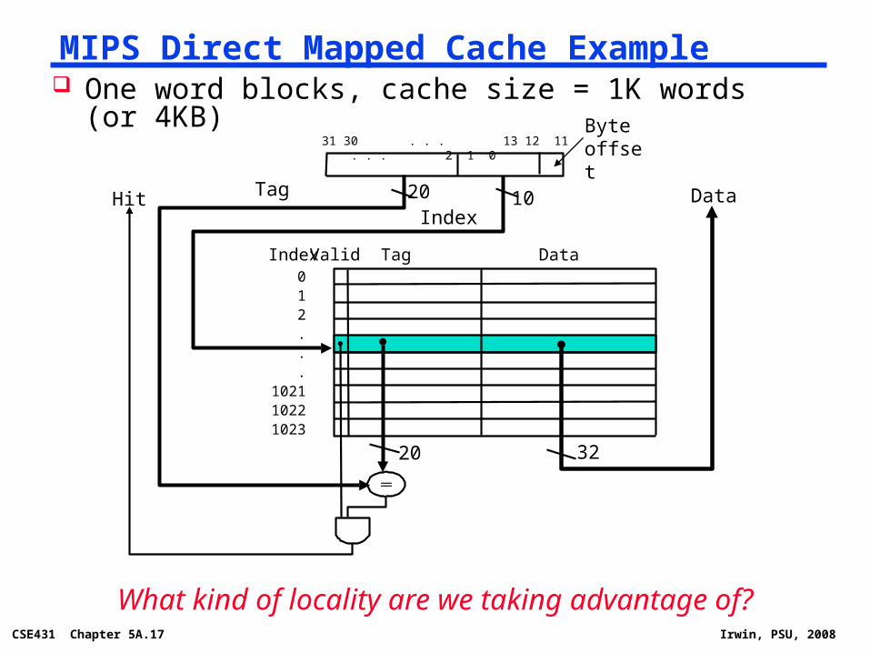
One word blocks, cache size = 1K words (or 4KB)MIPS Direct Mapped Cache Example
20Tag 10Index
Data Index TagValid012...
102110221023
31 30 . . . 13 12 11 . . . 2 1 0Byte offset
What kind of locality are we taking advantage of?
20
Data
32
Hit
CSE431 Chapter 5A.18 Irwin, PSU, 2008
Multiword Block Direct Mapped Cache
8Index
DataIndex TagValid012...
253254255
31 30 . . . 13 12 11 . . . 4 3 2 1 0Byte offset
20
20Tag
Hit Data
32
Block offset
Four words/block, cache size = 1K words
What kind of locality are we taking advantage of?
CSE431 Chapter 5A.20 Irwin, PSU, 2008
Taking Advantage of Spatial Locality
0
Let cache block hold more than one word 0 1 2 3 4 3 4 15
1 2
3 4 3
4 15
00 Mem(1) Mem(0)
miss
00 Mem(1) Mem(0)
hit
00 Mem(3) Mem(2)00 Mem(1) Mem(0)
miss
hit
00 Mem(3) Mem(2)00 Mem(1) Mem(0)
miss
00 Mem(3) Mem(2)00 Mem(1) Mem(0)
01 5 4hit
00 Mem(3) Mem(2)01 Mem(5) Mem(4)
hit
00 Mem(3) Mem(2)01 Mem(5) Mem(4)
00 Mem(3) Mem(2)01 Mem(5) Mem(4)
miss
11 15 14
Start with an empty cache - all blocks initially marked as not valid
8 requests, 4 misses
CSE431 Chapter 5A.21 Irwin, PSU, 2008
Miss Rate vs Block Size vs Cache Size
16 32 64 128 2560
5
10
8 KB
16 KB
64 KB
256 KB
Block size (bytes)
Mis
s ra
te (
%)
Miss rate goes up if the block size becomes a significant fraction of the cache size because the number of blocks that can be held in the same size cache is smaller (increasing capacity misses)
CSE431 Chapter 5A.22 Irwin, PSU, 2008
Cache Field Sizes
The number of bits in a cache includes both the storage for data and for the tags
32-bit byte address For a direct mapped cache with 2n blocks, n bits are used for the
index For a block size of 2m words (2m+2 bytes), m bits are used to
address the word within the block and 2 bits are used to address the byte within the word
What is the size of the tag field? The total number of bits in a direct-mapped cache is then
2n x (block size + tag field size + valid field size)
How many total bits are required for a direct mapped cache with 16KB of data and 4-word blocks assuming a 32-bit address?
CSE431 Chapter 5A.23 Irwin, PSU, 2008
Read hits (I$ and D$) this is what we want!
Write hits (D$ only) require the cache and memory to be consistent
- always write the data into both the cache block and the next level in the memory hierarchy (write-through)
- writes run at the speed of the next level in the memory hierarchy – so slow! – or can use a write buffer and stall only if the write buffer is full
allow cache and memory to be inconsistent- write the data only into the cache block (write-back the cache block to
the next level in the memory hierarchy when that cache block is “evicted”)
- need a dirty bit for each data cache block to tell if it needs to be written back to memory when it is evicted – can use a write buffer to help “buffer” write-backs of dirty blocks
Handling Cache Hits
CSE431 Chapter 5A.24 Irwin, PSU, 2008
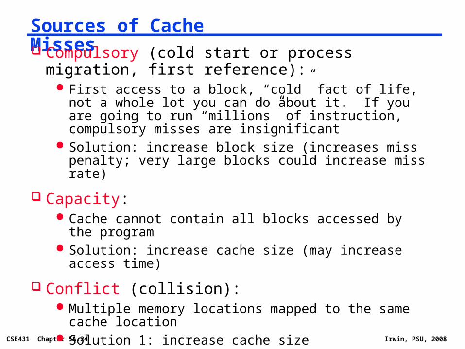
Sources of Cache Misses Compulsory (cold start or process migration, first
reference): First access to a block, “cold” fact of life, not a whole lot you
can do about it. If you are going to run “millions” of instruction, compulsory misses are insignificant
Solution: increase block size (increases miss penalty; very large blocks could increase miss rate)
Capacity: Cache cannot contain all blocks accessed by the program Solution: increase cache size (may increase access time)
Conflict (collision): Multiple memory locations mapped to the same cache location Solution 1: increase cache size Solution 2: increase associativity (stay tuned) (may increase
access time)
CSE431 Chapter 5A.25 Irwin, PSU, 2008
Handling Cache Misses (Single Word Blocks) Read misses (I$ and D$)
stall the pipeline, fetch the block from the next level in the memory hierarchy, install it in the cache and send the requested word to the processor, then let the pipeline resume
Write misses (D$ only)1. stall the pipeline, fetch the block from next level in the memory
hierarchy, install it in the cache (which may involve having to evict a dirty block if using a write-back cache), write the word from the processor to the cache, then let the pipeline resume
or
2. Write allocate – just write the word into the cache updating both the tag and data, no need to check for cache hit, no need to stall
or
3. No-write allocate – skip the cache write (but must invalidate that cache block since it will now hold stale data) and just write the word to the write buffer (and eventually to the next memory level), no need to stall if the write buffer isn’t full
CSE431 Chapter 5A.26 Irwin, PSU, 2008
Multiword Block Considerations
Read misses (I$ and D$) Processed the same as for single word blocks – a miss returns
the entire block from memory Miss penalty grows as block size grows
- Early restart – processor resumes execution as soon as the requested word of the block is returned
- Requested word first – requested word is transferred from the memory to the cache (and processor) first
Nonblocking cache – allows the processor to continue to access the cache while the cache is handling an earlier miss
Write misses (D$) If using write allocate must first fetch the block from memory and
then write the word to the block (or could end up with a “garbled” block in the cache (e.g., for 4 word blocks, a new tag, one word of data from the new block, and three words of data from the old block)
CSE431 Chapter 5A.27 Irwin, PSU, 2008
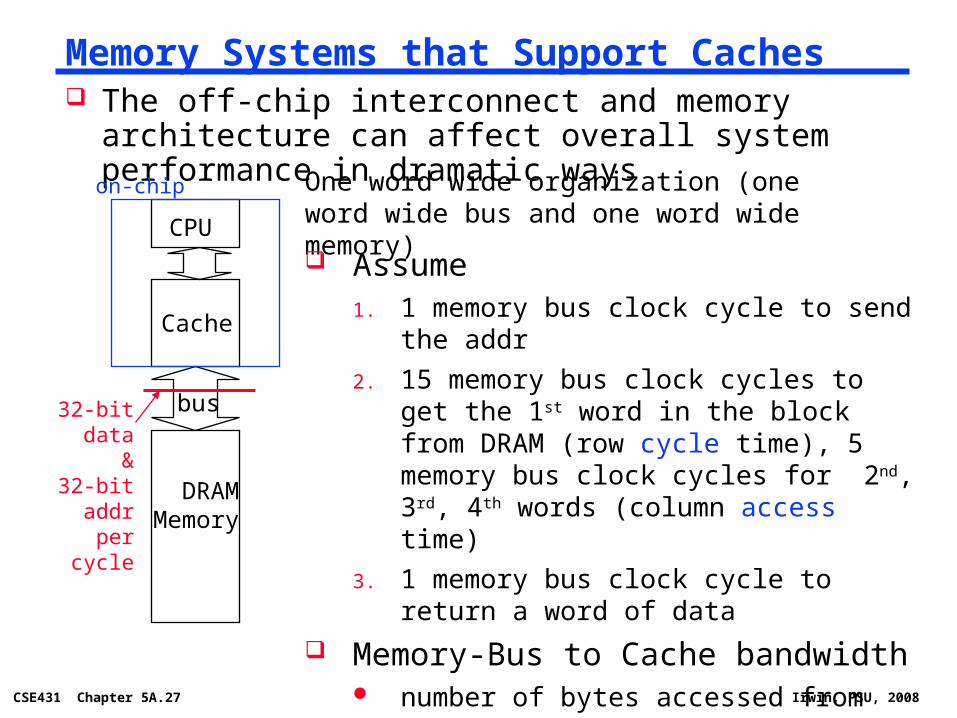
The off-chip interconnect and memory architecture can affect overall system performance in dramatic ways
Memory Systems that Support Caches
CPU
Cache
DRAMMemory
bus
One word wide organization (one word wide bus and one word wide memory)
Assume1. 1 memory bus clock cycle to send the addr
2. 15 memory bus clock cycles to get the 1st word in the block from DRAM (row cycle time), 5 memory bus clock cycles for 2nd, 3rd, 4th words (column access time)
3. 1 memory bus clock cycle to return a word of data
Memory-Bus to Cache bandwidth number of bytes accessed from memory
and transferred to cache/CPU per memory bus clock cycle
32-bit data&
32-bit addrper cycle
on-chip
CSE431 Chapter 5A.28 Irwin, PSU, 2008
Review: (DDR) SDRAM Operation
N r
ows
N cols
DRAM
ColumnAddress
M-bit Output
M bit planes N x M SRAM
RowAddress
After a row is read into the SRAM register
Input CAS as the starting “burst” address along with a burst length
Transfers a burst of data (ideally a cache block) from a series of sequential addr’s within that row- The memory bus clock controls
transfer of successive words in the burst
+1
Row Address
CAS
RAS
Col Address
1st M-bit Access 2nd M-bit 3rd M-bit 4th M-bit
Cycle Time
Row Add
CSE431 Chapter 5A.31 Irwin, PSU, 2008
One Word Wide Bus, One Word Blocks
CPU
Cache
DRAMMemory
bus
on-chip
If the block size is one word, then for a memory access due to a cache miss, the pipeline will have to stall for the number of cycles required to return one data word from memory
memory bus clock cycle to send address
memory bus clock cycles to read DRAM
memory bus clock cycle to return data
total clock cycles miss penalty
Number of bytes transferred per clock cycle (bandwidth) for a single miss is
bytes per memory bus clock cycle
1
15
1
17
4/17 = 0.235
CSE431 Chapter 5A.33 Irwin, PSU, 2008
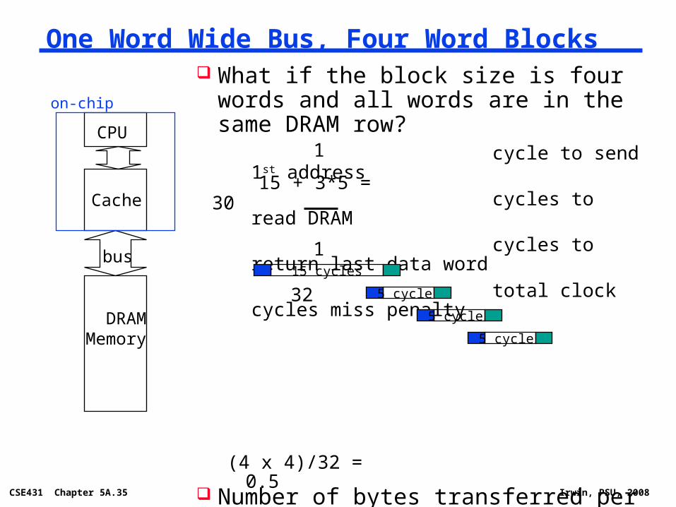
One Word Wide Bus, Four Word Blocks
CPU
Cache
DRAMMemory
bus
on-chip
What if the block size is four words and each word is in a different DRAM row?
cycle to send 1st address
cycles to read DRAM
cycles to return last data word
total clock cycles miss penalty
Number of bytes transferred per clock cycle (bandwidth) for a single miss is
bytes per clock
15 cycles
15 cycles
15 cycles
15 cycles
1
4 x 15 = 60
1
62
(4 x 4)/62 = 0.258
CSE431 Chapter 5A.35 Irwin, PSU, 2008
One Word Wide Bus, Four Word Blocks
CPU
Cache
DRAMMemory
bus
on-chip
What if the block size is four words and all words are in the same DRAM row?
cycle to send 1st address
cycles to read DRAM
cycles to return last data word
total clock cycles miss penalty
Number of bytes transferred per clock cycle (bandwidth) for a single miss is
bytes per clock
15 cycles
5 cycles
5 cycles
5 cycles
1
15 + 3*5 = 30
1
32
(4 x 4)/32 = 0.5
CSE431 Chapter 5A.37 Irwin, PSU, 2008
Interleaved Memory, One Word Wide Bus
For a block size of four words cycle to send 1st address
cycles to read DRAM banks
cycles to return last data word
total clock cycles miss penalty
CPU
Cache
bus
on-chip
Number of bytes transferred per clock cycle (bandwidth) for a single miss is
bytes per clock
15 cycles
15 cycles
15 cycles
15 cycles
(4 x 4)/20 = 0.8
1
15
4*1 = 4
20
DRAMMemorybank 1
DRAMMemorybank 0
DRAMMemorybank 2
DRAMMemorybank 3
CSE431 Chapter 5A.38 Irwin, PSU, 2008
DRAM Memory System Summary
Its important to match the cache characteristics caches access one block at a time (usually more than one
word)
with the DRAM characteristics use DRAMs that support fast multiple word accesses,
preferably ones that match the block size of the cache
with the memory-bus characteristics make sure the memory-bus can support the DRAM access
rates and patterns with the goal of increasing the Memory-Bus to Cache
bandwidth
CSE431 Chapter 5A.39 Irwin, PSU, 2008
Measuring Cache Performance Assuming cache hit costs are included as part of the
normal CPU execution cycle, thenCPU time = IC × CPI × CC
= IC × (CPIideal + Memory-stall cycles) × CC
CPIstall
Memory-stall cycles come from cache misses (a sum of read-stalls and write-stalls)
Read-stall cycles = reads/program × read miss rate × read miss penalty
Write-stall cycles = (writes/program × write miss rate × write miss penalty)
+ write buffer stalls
For write-through caches, we can simplify this toMemory-stall cycles = accesses/program × miss rate × miss penalty
CSE431 Chapter 5A.40 Irwin, PSU, 2008
Impacts of Cache Performance Relative cache penalty increases as processor
performance improves (faster clock rate and/or lower CPI) The memory speed is unlikely to improve as fast as processor
cycle time. When calculating CPIstall, the cache miss penalty is measured in processor clock cycles needed to handle a miss
The lower the CPIideal, the more pronounced the impact of stalls
A processor with a CPIideal of 2, a 100 cycle miss penalty, 36% load/store instr’s, and 2% I$ and 4% D$ miss rates
What if the CPIideal is reduced to 1? 0.5? 0.25? What if the D$ miss rate went up 1%? 2%? What if the processor clock rate is doubled (doubling the
miss penalty)?
CSE431 Chapter 5A.41 Irwin, PSU, 2008
Average Memory Access Time (AMAT)
A larger cache will have a longer access time. An increase in hit time will likely add another stage to the pipeline. At some point the increase in hit time for a larger cache will overcome the improvement in hit rate leading to a decrease in performance.
Average Memory Access Time (AMAT) is the average to access memory considering both hits and misses
AMAT = Time for a hit + Miss rate x Miss penalty
What is the AMAT for a processor with a 20 psec clock, a miss penalty of 50 clock cycles, a miss rate of 0.02 misses per instruction and a cache access time of 1 clock cycle?
CSE431 Chapter 5A.42 Irwin, PSU, 2008
Reducing Cache Miss Rates #1
1. Allow more flexible block placement
In a direct mapped cache a memory block maps to exactly one cache block
At the other extreme, could allow a memory block to be mapped to any cache block – fully associative cache
A compromise is to divide the cache into sets each of which consists of n “ways” (n-way set associative). A memory block maps to a unique set (specified by the index field) and can be placed in any way of that set (so there are n choices)
(block address) modulo (# sets in the cache)
CSE431 Chapter 5A.44 Irwin, PSU, 2008
Another Reference String Mapping
0 4 0 4
0 4 0 4
Consider the main memory word reference string 0 4 0 4 0 4 0 4
miss miss miss miss
miss miss miss miss
00 Mem(0) 00 Mem(0)01 4
01 Mem(4)000
00 Mem(0)01
4
00 Mem(0)01 4
00 Mem(0)01
401 Mem(4)
00001 Mem(4)
000
Start with an empty cache - all blocks initially marked as not valid
Ping pong effect due to conflict misses - two memory locations that map into the same cache block
8 requests, 8 misses
CSE431 Chapter 5A.45 Irwin, PSU, 2008
Set Associative Cache Example
0
Cache
Main Memory
Q2: How do we find it?
Use next 1 low order memory address bit to determine which cache set (i.e., modulo the number of sets in the cache)
Tag Data
Q1: Is it there?
Compare all the cache tags in the set to the high order 3 memory address bits to tell if the memory block is in the cache
One word blocksTwo low order bits define the byte in the word (32b words)
CSE431 Chapter 5A.47 Irwin, PSU, 2008
Another Reference String Mapping
0 4 0 4
Consider the main memory word reference string 0 4 0 4 0 4 0 4
miss miss hit hit
000 Mem(0) 000 Mem(0)
Start with an empty cache - all blocks initially marked as not valid
010 Mem(4) 010 Mem(4)
000 Mem(0) 000 Mem(0)
010 Mem(4)
Solves the ping pong effect in a direct mapped cache due to conflict misses since now two memory locations that map into the same cache set can co-exist!
8 requests, 2 misses
CSE431 Chapter 5A.48 Irwin, PSU, 2008
Four-Way Set Associative Cache 28 = 256 sets each with four ways (each with one block)
31 30 . . . 13 12 11 . . . 2 1 0 Byte offset
DataTagV012...
253 254 255
DataTagV012...
253 254 255
DataTagV012...
253 254 255
Index DataTagV012...
253 254 255
8Index
22Tag
Hit Data
32
4x1 select
Way 0 Way 1 Way 2 Way 3
CSE431 Chapter 5A.50 Irwin, PSU, 2008
Range of Set Associative Caches For a fixed size cache, each increase by a factor of two
in associativity doubles the number of blocks per set (i.e., the number or ways) and halves the number of sets – decreases the size of the index by 1 bit and increases the size of the tag by 1 bit
Block offset Byte offsetIndexTag
Decreasing associativity
Fully associative(only one set)Tag is all the bits exceptblock and byte offset
Direct mapped(only one way)Smaller tags, only a single comparator
Increasing associativity
Selects the setUsed for tag compare Selects the word in the block
CSE431 Chapter 5A.51 Irwin, PSU, 2008
Costs of Set Associative Caches When a miss occurs, which way’s block do we pick for
replacement? Least Recently Used (LRU): the block replaced is the one that
has been unused for the longest time- Must have hardware to keep track of when each way’s block was
used relative to the other blocks in the set- For 2-way set associative, takes one bit per set → set the bit when a
block is referenced (and reset the other way’s bit)
N-way set associative cache costs N comparators (delay and area) MUX delay (set selection) before data is available Data available after set selection (and Hit/Miss decision). In a
direct mapped cache, the cache block is available before the Hit/Miss decision
- So its not possible to just assume a hit and continue and recover later if it was a miss
CSE431 Chapter 5A.52 Irwin, PSU, 2008
Benefits of Set Associative Caches The choice of direct mapped or set associative depends
on the cost of a miss versus the cost of implementation
0
2
4
6
8
10
12
1-way 2-way 4-way 8-way
Associativity
Mis
s R
ate
4KB8KB16KB32KB64KB128KB256KB512KB
Data from Hennessy & Patterson, Computer Architecture, 2003
Largest gains are in going from direct mapped to 2-way (20%+ reduction in miss rate)
CSE431 Chapter 5A.53 Irwin, PSU, 2008
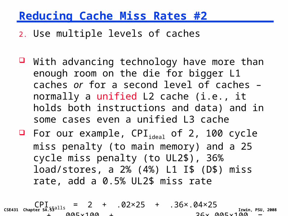
Reducing Cache Miss Rates #2
2. Use multiple levels of caches
With advancing technology have more than enough room on the die for bigger L1 caches or for a second level of caches – normally a unified L2 cache (i.e., it holds both instructions and data) and in some cases even a unified L3 cache
For our example, CPIideal of 2, 100 cycle miss penalty (to main memory) and a 25 cycle miss penalty (to UL2$), 36% load/stores, a 2% (4%) L1 I$ (D$) miss rate, add a 0.5% UL2$ miss rate
Multilevel Cache Design Considerations Design considerations for L1 and L2 caches are very
different Primary cache should focus on minimizing hit time in support of
a shorter clock cycle- Smaller with smaller block sizes
Secondary cache(s) should focus on reducing miss rate to reduce the penalty of long main memory access times
- Larger with larger block sizes- Higher levels of associativity
The miss penalty of the L1 cache is significantly reduced by the presence of an L2 cache – so it can be smaller (i.e., faster) but have a higher miss rate
For the L2 cache, hit time is less important than miss rate The L2$ hit time determines L1$’s miss penalty L2$ local miss rate >> than the global miss rate
CSE431 Chapter 5A.56 Irwin, PSU, 2008
Two Machines’ Cache Parameters
Intel Nehalem AMD Barcelona
L1 cache organization & size
Split I$ and D$; 32KB for each per core; 64B blocks
Split I$ and D$; 64KB for each per core; 64B blocks
L1 associativity 4-way (I), 8-way (D) set assoc.; ~LRU replacement
Cache Coherence in Multicores In future multicore processors its likely that the cores will
share a common physical address space, causing a cache coherence problem
Core 1 Core 2
L1 I$ L1 D$
Unified (shared) L2
L1 I$ L1 D$
X = 0
X = 0 X = 0
Read X Read X
Write 1 to X
X = 1
X = 1
CSE431 Chapter 5A.62 Irwin, PSU, 2008
A Coherent Memory System
Any read of a data item should return the most recently written value of the data item
Coherence – defines what values can be returned by a read- Writes to the same location are serialized (two writes to the same
location must be seen in the same order by all cores)
Consistency – determines when a written value will be returned by a read
To enforce coherence, caches must provide Replication of shared data items in multiple cores’ caches
Replication reduces both latency and contention for a read shared data item
Migration of shared data items to a core’s local cache Migration reduced the latency of the access the data and the
bandwidth demand on the shared memory (L2 in our example)
CSE431 Chapter 5A.63 Irwin, PSU, 2008
Cache Coherence Protocols Need a hardware protocol to ensure cache coherence
the most popular of which is snooping The cache controllers monitor (snoop) on the broadcast medium
(e.g., bus) with duplicate address tag hardware (so they don’t interfere with core’s access to the cache) to determine if their cache has a copy of a block that is requested
Write invalidate protocol – writes require exclusive access and invalidate all other copies
Exclusive access ensure that no other readable or writable copies of an item exists
If two processors attempt to write the same data at the same time, one of them wins the race causing the other core’s copy to be invalidated. For the other core to complete, it must obtain a new copy of the data which must now contain the updated value – thus enforcing write serialization
CSE431 Chapter 5A.66 Irwin, PSU, 2008
Example of Snooping Invalidation
When the second miss by Core 2 occurs, Core 1 responds with the value canceling the response from the L2 cache (and also updating the L2 copy)
Core 1 Core 2
L1 I$ L1 D$
Unified (shared) L2
L1 I$ L1 D$
X = 0
X = 0 X = 0
Read X Read X
Write 1 to X
X = 1
Read X
X = I
X = IX = 1
X = 1
CSE431 Chapter 5A.68 Irwin, PSU, 2008
A Write-Invalidate CC Protocol
Shared(clean)
Invalid
Modified(dirty)
write-back caching protocol in black
read (miss)
write (h
it or m
iss)
read (hit or miss)
read (hit) or write (hit)
writ
e (m
iss)
send in
validate
receives invalidate(write by another core
to this block)w
rite-
back
due
to
read
(m
iss)
by
anot
her
core
to
this
blo
ck
send
inva
lidat
e
signals from the core in redsignals from the bus in blue
CSE431 Chapter 5A.71 Irwin, PSU, 2008
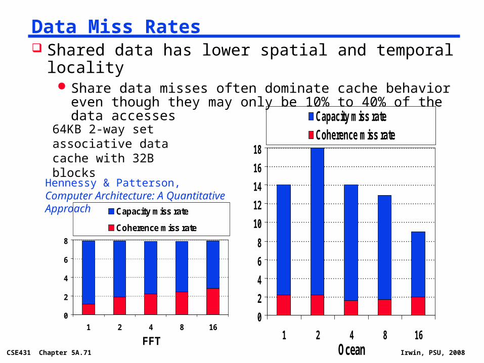
Data Miss Rates Shared data has lower spatial and temporal locality
Share data misses often dominate cache behavior even though they may only be 10% to 40% of the data accesses
FFT
0
2
4
6
8
1 2 4 8 16
Capacity miss rate
Coherence miss rate
Ocean
0
2
4
6
8
10
12
14
16
18
1 2 4 8 16
Capacity miss rateCoherence miss rate64KB 2-way set associative
data cache with 32B blocks
Hennessy & Patterson, Computer Architecture: A Quantitative Approach
CSE431 Chapter 5A.72 Irwin, PSU, 2008
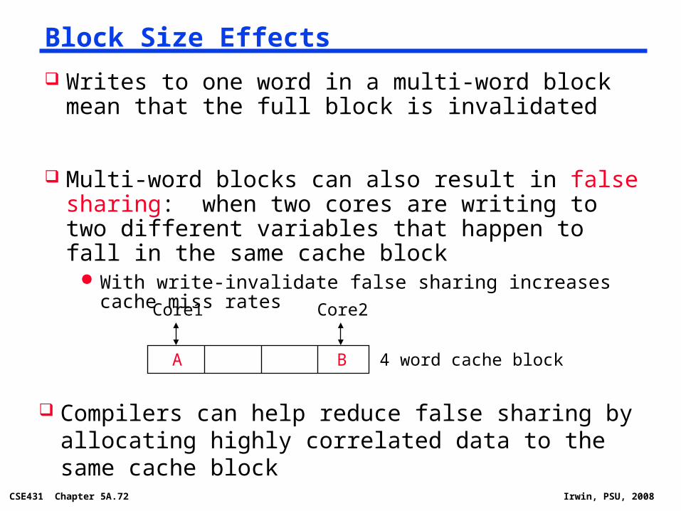
Block Size Effects
Writes to one word in a multi-word block mean that the full block is invalidated
Multi-word blocks can also result in false sharing: when two cores are writing to two different variables that happen to fall in the same cache block
With write-invalidate false sharing increases cache miss rates
Compilers can help reduce false sharing by allocating highly correlated data to the same cache block
A B
Core1 Core2
4 word cache block
CSE431 Chapter 5A.73 Irwin, PSU, 2008
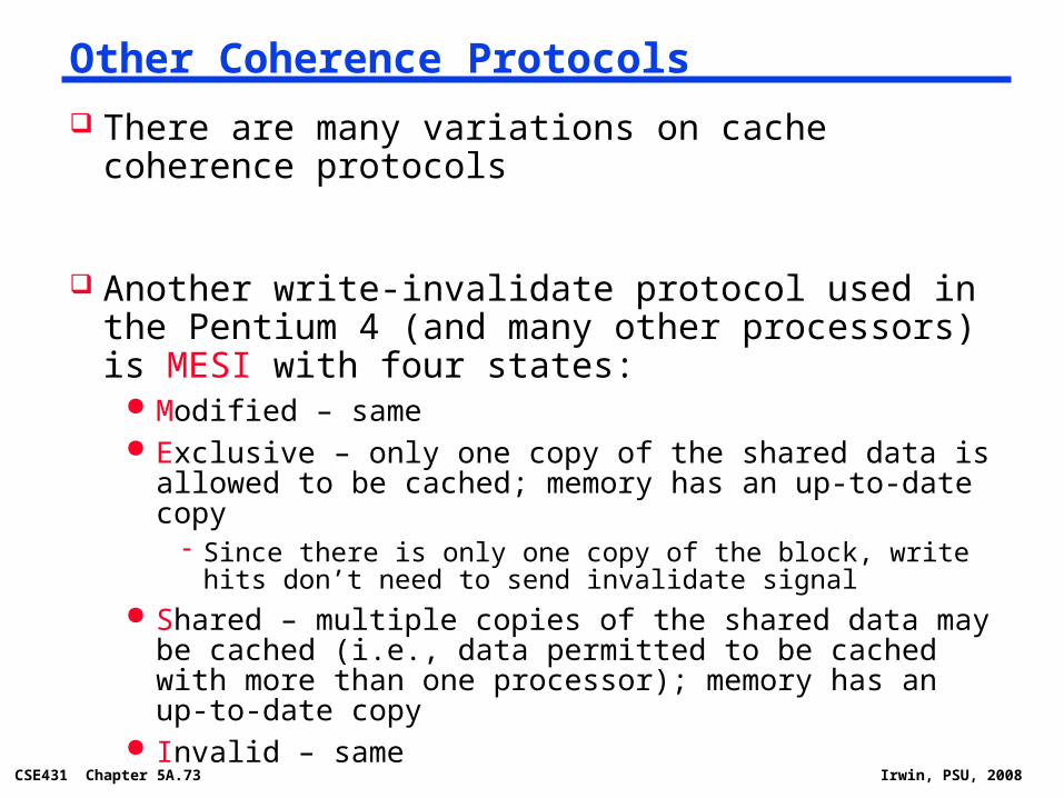
Other Coherence Protocols
There are many variations on cache coherence protocols
Another write-invalidate protocol used in the Pentium 4 (and many other processors) is MESI with four states:
Modified – same Exclusive – only one copy of the shared data is allowed to be
cached; memory has an up-to-date copy- Since there is only one copy of the block, write hits don’t need to
send invalidate signal Shared – multiple copies of the shared data may be cached (i.e.,
data permitted to be cached with more than one processor); memory has an up-to-date copy
Invalid – same
CSE431 Chapter 5A.75 Irwin, PSU, 2008
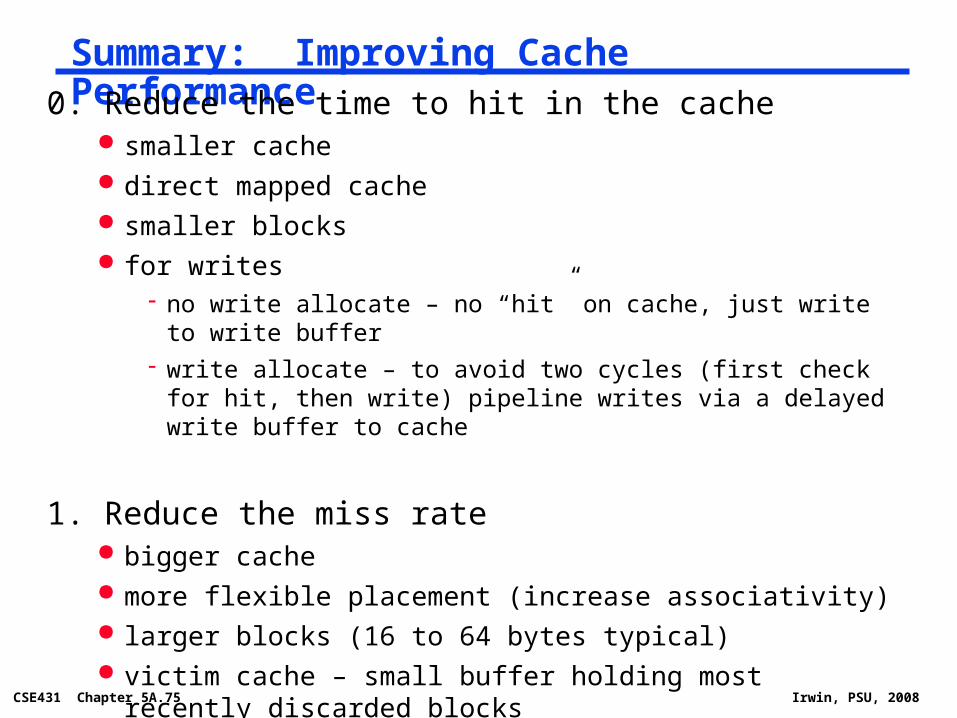
Summary: Improving Cache Performance0. Reduce the time to hit in the cache
smaller cache direct mapped cache smaller blocks for writes
- no write allocate – no “hit” on cache, just write to write buffer- write allocate – to avoid two cycles (first check for hit, then write)
pipeline writes via a delayed write buffer to cache
1. Reduce the miss rate bigger cache more flexible placement (increase associativity) larger blocks (16 to 64 bytes typical) victim cache – small buffer holding most recently discarded
blocks
CSE431 Chapter 5A.76 Irwin, PSU, 2008
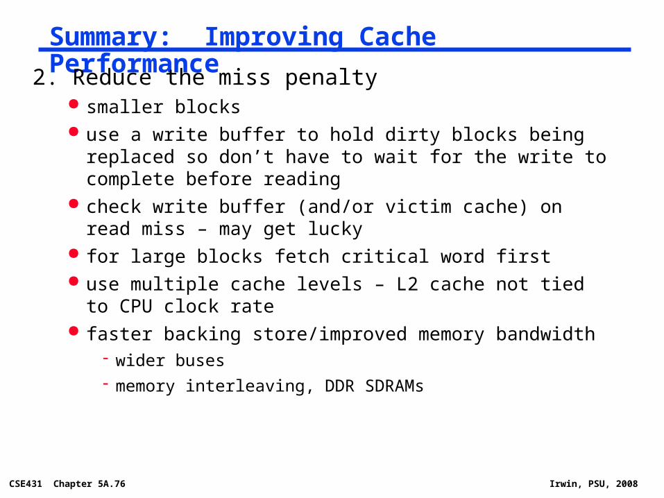
Summary: Improving Cache Performance
2. Reduce the miss penalty smaller blocks use a write buffer to hold dirty blocks being replaced so don’t
have to wait for the write to complete before reading check write buffer (and/or victim cache) on read miss – may get
lucky for large blocks fetch critical word first use multiple cache levels – L2 cache not tied to CPU clock rate faster backing store/improved memory bandwidth
- wider buses- memory interleaving, DDR SDRAMs
CSE431 Chapter 5A.77 Irwin, PSU, 2008
Summary: The Cache Design Space Several interacting dimensions
Reminders Quiz #4 will open next week and close October 23rd
HW4 due October 30th
HW5 out October 31th (spooky !)
Second evening midterm exam scheduled- Wednesday, November 18, 20:15 to 22:15, Location 262 Willard- Please let me know ASAP (via email) if you have a conflict