tiT^r The 8080 is a complete 8-bit parallel, central processor unit (CPU) for use in genera! purpose digital computer sys- tems. It is fabricated on a single LSI chip (see Figure 2-1). using Intel's n-channe) silicon gate MOS process. The 8080 transfers data and interna) state information via an 8-bit, bidirectional 3-state Data Bus (DQ-D7). Memory and peri- pheral device addresses are transmitted over a separate 16- bit 3-state Address Bus (A0-A15). Six timing and control outputs (SYNC, DBIN, WA)T,WR, HLDA and INTE) eman- ate from the 8080, while four control inputs (READY, HOLD, INT and RESET), four power inputs (+12v, +5v, -5v, and GND) and two clock inputs (01 and ^2) are ac- cepted by the 8080. MIT HEADY HLDA f "ruMm tMaEBPWtW, .duamamyta. w - An A,; A,3 A„ A„ ... J . . ^ . y s P r "t- '.' S L. < < .. ' . =- . - . A M ', ^ . ... r y W i . ti . . BiUtatC^mNA^ - ^ . .. GND O- D , O- D , O- ^ Dp O O, O O. 0 -5V O- RESET O HOLD O- INT O- INTE O- DBIN o - WR O- SYNC O- +5V O - 9 10 11 12 13 14 15 16 17 18 19 20 !NTEtT 8080 -O A^ -O A^ -O A^ - O A , 5 <-0 Ag -O Ag -O A? -O A. A5 -O A„ -O +HV -O A2 -O Ai -O A„ <-0 WAIT -O READY -O #1 Figure 2 1. 8080 Photomicrograph With Pin Designations 2-1
Transcript
t i T ^ r
The 8080 is a complete 8-bit parallel, central processor
unit (CPU) for use in genera! purpose digital computer sys-
tems. It is fabricated on a single LSI chip (see Figure 2-1).
using Intel's n-channe) silicon gate MOS process. The 8080
transfers data and interna) state information via an 8-bit,
bidirectional 3-state Data Bus (DQ-D7). Memory and peri-
pheral device addresses are transmitted over a separate 16-
bit 3-state Address Bus (A0-A15). Six timing and control
outputs (SYNC, DBIN, WA)T,WR, HLDA and INTE) eman-
ate from the 8080, while four control inputs (READY ,
HOLD, INT and RESET), four power inputs (+12v, +5v,
-5v, and GND) and two clock inputs (01 and ^2) are ac-
cepted by the 8080.
MIT HEADY HLDA f
"ruMm
tMaEBPWtW, .duamamyta.
w -
An A,; A,3 A„ A„
... J
. . ^ . y s P r "t-
'.' S L. < < ..
' . =- .
- . A M ', ^ .
... r y W i
. ti
.
. BiUtatC mNA - . ..
GND O-
D , O-
D , O-^
Dp O O, O
O. 0 - 5 V O-
RESET O
HOLD O-
INT O-
INTE O -
DBIN o -
WR O-
SYNC O -
+5V O -
9
10
11
12
13
14
15
16
17
18
19
20
! N T E t T
8080
-O A^
-O A^
-O A^
- O A , 5
<-0 Ag
-O Ag
- O A?
-O A. A5
- O A„
- O + H V
-O A2
-O Ai
-O A„
<-0 WAIT
- O R E A D Y
-O #1
Figure 2 1. 8080 Photomicrograph With Pin Designations
2-1
ARCHtTECTURE OF THE 8080 CPU
The 8080 CPU consists of the following functional
units:
* Register array and address logic
* Arithmetic and logic unit (ALU)
* Instruction register and control section
* Bi-directional, 3-state data bus buffer
Figure 2-2 illustrates the functional blocks within
the 8080 CPU.
Registers:
The register section consists of a static RAM array
organized into six 16-bit registers:
* Program counter (PC)
* Stack pointer (SP)
* Six 8-bit general purpose registers arranged in pairs,
referred to as B,C; D,E; and H,L
* A temporary register pair called W,Z
The program counter maintains the memory address
of the current program instruction and is incremented auto-
matically during every instruction fetch. The stack pointer
maintains the address of the next available stack location in
memory. The stack pointer can be initialized to use any
portion of read-write memory as a stack. The stack pointer
is decremented when data is "pushed" onto the stack and
incremented when data is " popped" off the stack (i.e., the
stack grows "downward" ) .
The six general purpose registers can be used either as
single registers (8-bit) or as register pairs (16-bit). The
temporary register pair, W,Z, is not program addressable
and is only used for the internal execution of instructions.
Eight-bit data bytes can be transferred between the
internal bus and the register array via the register-select
multiplexer. Sixteen-bit transfers can proceed between the
register array and the address latch or the incrementer/
decrementer circuit. The address latch receives data from
any of the three register pairs and drives the 16 address
output buffers (A0-A15), as well as the incrementer/
decrementer circuit. The incrementer/decrementer circuit
receives data from the address latch and sends it to
the register array. The 16-bit data can be incremented or
decremented or simply transferred between registers.
Di D„ BI-DIRECTIONAL
DATA BUS
DATA BUS INTERRUPT HOLD WAIT
WRITE CONTROL CONTROL CONTROL CONTROL SYNC CLOCKS
INTE INT HOLDHOLDWAIT SYNC < 2 RESET
ACK READY ADDRESS BUS
Figure 2 2. 8080 CPU Functional Block Diagram
2 2
Arithmetic and Logic Unit (ALU):
The ALU contains the following registers:
* An 8-bit accumulator
* An 8-bit temporary accumulator (ACT)
* A 5-bit flag register: zero, carry, sign, parity and
auxiliary carry
* An 8-bit temporary register (TMP)
Arithmetic, logical and rotate operations are per-
formed in the ALU. The ALU is fed by the temporary
register (TMP) and the temporary accumulator (ACT) and
carry flip-flop. The result of the operation can be trans-
ferred to the internal bus or to the accumulator; the ALU
also feeds the flag register.
The temporary register (TMP) receives information
from the internal bus and can send all or portions of it to
the ALU, the flag register and the internal bus.
The accumulator (ACC) can be loaded from the ALU
and the internal bus and can transfer data to the temporary
accumulator (ACT) and the internal bus. The contents of
the accumulator (ACC) and the auxiliary carry flip-flop can
be tested for decimal correction during the execution of the
DAA instruction (see Chapter 4).
tnstruction Register and Contro!:
During an instruction fetch, the first byte of an in-
struction (containing the OP code) is transferred from the
internal bus to the 8-bit instruction register.
The contents of the instruction register are, in turn,
available to the instruction decoder. The output of the
decoder, combined with various timing signals, provides
the control signals for the register array, ALU and data
buffer blocks. In addition, the outputs from the instruction
decoder and external control signals feed the timing and
state control section which generates the state and cycle
timing signals.
Data Bus Buffer:
This 8-bit bidirectional 3-state buffer is used to
isolate the CPU's internal bus from the external data bus.
(Do through Dy). In the output mode, the internal bus
content is loaded into an 8-bit latch that, in turn, drives the
data bus output buffers. The output buffers are switched
off during input or non-transfer operations.
During the input mode, data from the external data bus
is transferred to the internal bus. The internal bus is pre-
charged at the beginning of each internal state, except for
the transfer state (T3—described later in this chapter).
THE PROCESSOR CYCLE
An instruction cycte is defined as the time required
to fetch and execute an instruction. During the fetch, a
selected instruction (one, two or three bytes) is extracted
from memory and deposited in the CPU's instruction regis-
ter. During the execution phase, the instruction is decoded
and translated into specific processing activities.
Every instruction cycle consists of one, two, three,
four or five machine cycles. A machine cycte is required
each time the CPU accesses memory or an I/O port. The
fetch portion of an instruction cycle requires one machine
cycle for each byte to be fetched. The duration of the execu-
tion portion of the instruction cycle depends on the kind
of instruction that has been fetched. Some instructions do
not require any machine cycles other than those necessary
to fetch the instruction; other instructions, however, re-
quire additional machine cycles to write or read data to/
from memory or I/O devices. The D A D instruction is an
exception in that it requires two additional machine cycles
to complete an internal register-pair add (see Chapter 4).
Each machine cycle consists of three, four or five
states. A state is the smallest unit of processing activity and
is defined as the interval between two successive positive-
going transitions of the 01 driven clock pulse. The 8080
isdriven by a two-phase clock oscillator. All processing activ-
ities are referred to the period of this clock. The two non-
overlapping clock pulses, labeled 01 and 02. are furnished
by external circuitry. It is the 01 clock pulse which divides
each machine cycle into states. Timing logic within the
8080 uses the clock inputs to produce a SYNC pulse,
which identifies the beginning of every machine cycle. The
SYNC pulse is triggered by the low-to-high transition of 02,
as shown in Figure 2-3.
^ —
FIRST STATE OF
' EVERY MACHINE
CYCLE
/ \ ^ —
/ \ / \
SYNC SYNC / \
' SYNC DOES NOT OCCUR IN THE SECOND AND THIRD MACHINE
CYCLES OF A DAD INSTRUCTION SINCE THESE MACHINE CYCLES
ARE USED FOR AN INTERNAL REGISTER-PAIR ADD.
Figure 2 3 . 0 1 , 0 2 And SYNC Timing
There are three exceptions to the defined duration of
a state. They are the WAIT state, the hold (HLDA) state
and the halt (HLTA) state, described later in this chapter.
Because the WAIT, the HLDA , and the HLTA states depend
upon external events, they are by their nature of indeter-
minate length. Even these exceptional states, however, must
2-3
be synchronized with the pulses of the driving clock. Thus,
the duration of all states are integral multiples of the clock
period.
To summarize then, each ctock period marks a state;
three to five states constitute a machine cycle; and one to
five machine cycles comprise an instruction cycte. A full
instruction cycle requires anywhere from four to eight-
teen states for its completion, depending on the kind of in-
struction involved.
Machine Cycte tdentification:
With the exception of the D A D instruction, there is
just one consideration that determines how many machine
cycles are required in any given instruction cycle: the num-
ber of times that the processor must reference a memory
address or an addressable peripheral device, in order to
fetch and execute the instruction. Like many processors,
the 8080 is so constructed that it can transmit only one
address per machine cycle. Thus, if the fetch and execution
of an instruction requires two memory references, then the
instruction cycle associated with that instruction consists of
two machine cycles. If five such references are called for,
then the instruction cycle contains five machine cycles.
Every instruction cycle has at least one reference to
memory, during which the instruction is fetched. An in-
struction cycle must always have a fetch, even if the execu-
tion of the instruction requires no further references to
memory. The first machine cycle in every instruction cycle
is therefore a FETCH. Beyond that, there are no fast rules.
It depends on the kind of instruction that is fetched.
Consider some examples. The add-register (ADD r)
instruction is an instruction that requires only a single
machine cycle (FETCH) for its completion. In this one-byte
instruction, the contents of one of the CPU's six general
purpose registers is added to the existing contents of the
accumulator. Since all the information necessary to execute
the command is contained in the eight bits of the instruction
code, only one memory reference is necessary. Three states
are used to extract the instruction from memory, and one
additional state is used to accomplish the desired addit ion.
The entire instruction cycle thus requires only one machine
cycle that consists of four states, or four periods of the ex-
terna) clock.
Suppose now, however, that we wish to add the con-
tents of a specific memory location to the existing contents
of the accumulator (ADD M). Although this is quite similar
in principle to the example just cited, several additional
steps will be used. An extra machine cycle will be used, in
order to address the desired memory location.
The actual sequence is as follows. First the processor
extracts from memory the one-byte instruction word ad-
dressed by its program counter. This takes three states.
The eight-bit instruction word obtained during the FETCH
machine cycle is deposited in the CPU's instruction register
and used to direct activities during the remainder of the
instruction cycle. Next, the processor sends out,as an address,
the contents of its H and L registers. The eight-bit data
word returned during this M E M O R Y R E A D machine cycle
is placed in a temporary register inside the 8080 CPU. By
now three more clock periods (states) have elapsed. In the
seventh and final state, the contents of the temporary regis-
ter are added to those of the accumulator. Two machine
cycles, consisting of seven states in all, complete the
" A D D M " instruction cycle.
A t the opposite extreme is the save H and L registers
(SHLD) instruction, which requires five machine cycles.
During an " S H L D " instruction cycte, the contents of the
processor's H and L registers are deposited in two sequen-
tially adjacent memory locations; the destination is indi-
cated by two address bytes which are stored in the two
memory locations immediately following the operation code
byte. The following sequence of events occurs:
(1) A FETCH machine cycle, consisting of four
states. During the first three states of this
machine cycle, the processor fetches the instruc-
tion indicated by its program counter. The pro-
gram counter is then incremented. The fourth
state is used for internal instruction decoding.
(2) A M E M O R Y R E A D machine cycle, consisting
of three states. During this machine cycle, the
byte indicated by the program counter is read
from memory and placed in the processor's
Z register. The program counter is incremented
again.
(3) Another M E M O R Y R E A D machine cycle, con-
sisting of three states, in which the byte indica-
ted by the processor's program counter is read
from memory and placed in the W register. The
program counter is incremented, in anticipation
of the next instruction fetch.
(4) A M E M O R Y WRtTE machine cycle, of three
states, in which the contents of the L register
are transferred to the memory location pointed
to by the present contents of the W and Z regis-
ters. The state following the transfer is used to
increment the W,Z register pair so that it indi-
cates the next memory location to receive data.
(5) A M E M O R Y WRtTE machine cycle, of three
states, in which the contents of the H register
are transferred to the new memory location
pointed to by the W,Z register pair.
In summary, the " S H L D " instruction cycle contains
five machine cycles and takes 16 states to execute.
Most instructions fall somewhere between the ex-
tremes typified by the " A D D r " and the " S H L D " instruc-
tions. The input (INP) and the ou tpu t (OUT) instructions,
for example, require three machine cycles: a FETCH, to
obtain the instruction; a M E M O R Y R E A D , to obtain the
address of the object peripherat; and an tNPUT or an OUT-
PUT machine cycle, to complete the transfer.
2-4
White no one instruction cycle will consist o f more
then five machine cycles, the fo l lowing ten different types
of machine cycles may occur wi th in an instruction cycle:
(1) FETCH (M1)
(2) M E M O R Y R E A D
(3) M E M O R Y W R I T E
(4) STACK R E A D
(5) STACK W R I T E
(6) tNPUT
(7) O U T P U T
(8) I N T E R R U P T
(9) H A L T
(10) H A L T . I N T E R R U P T
The machine cycles that actual ly do occur in a par-
ticular instruction cycle depend upon the k ind of instruc-
t ion , wi th the overriding st ipulat ion that the first machine
cycle in any instruction cycle is always a FETCH.
The processor identifies the machine cycle in prog-
ress by transmitt ing an eight-bit status word during the first
state of every machine cycle. Updated status in format ion is
presented on the 8080's data lines (D0-D7), dur ing the
S Y N C interval. This data should be saved in latches, and
used to develop control signals for external circuitry. Table
2-1 shows how the positive-true status in format ion is dis-
tr ibuted on the processor's data bus.
Status signals are provided principally for the control
of external circuitry. S impl ic i ty of interface, rather than
machine cycle identif icat ion, dictates the logical def in i t ion
of individual status bits. Y o u will therefore observe that
certain processor machine cycles are uniquely identif ied by
a single status bit , but that others are not . The M^ status
bit (Dg) , for example, unambiguous ly identifies a FETCH
machine cycle. A STACK R E A D , on the other hand, is
indicated by the coincidence o f STACK and MEtVtR sig-
nals. Machine cycle identif icat ion data is also valuable in
the test and de-bugging phases of system development .
Table 2-1 lists the status bit ou tpu ts for each type of
machine cycle.
State Transition Sequence:
Every machine cycle wi th in an instruction cycle con-
sists of three to five active states (referred to as T^ , T2, T3,
T4, T5 or T w ) . The actual number of states depends upon
the instruction being executed, and on the particular ma-
chine cycle w i th in the greater instruction cycle. The state
transition diagram in Figure 2-4 shows how the 8080 pro-
ceeds f rom state to state in the course of a mach ine cycle.
The diagram also shows how the R E A D Y , H O L D , and
I N T E R R U P T lines are sampled dur ing the mach ine cycle,
and how the condi t ions on these lines may mod i fy the
basic transit ion sequence, tn the present discussion, we are
concerned on ly wi th the basic sequence and with the
R E A D Y func t ion . The H O L D and I N T E R R U P T funct ions
will be discussed later.
The 8080 CPU does not directly indicate its internal
state by transmitt ing a "state con t r o l " ou tpu t dur ing
each state; instead, the 8080 supplies direct control ou tpu t
( INTE, H L D A , D B I N , W R and WA IT ) for use by external
circuitry.
Recall that the 8080 passes through at least three
states in every machine cycle, wi th each state def ined by
successive low-to-high transit ions of the 01 clock. Figure
2-5 shows the t iming relationships in a typical FETCH
machine cycle. Events that occur in each state are referenced
to transit ions of the 0 i and 02 clock pulses.
The S Y N C signal identifies the first state (T-]) in
every machine cycle. As shown in Figure 2-5, the S Y N C
signal is related to the leading edge of the 02 clock. There is
a delay ( t p c ) between the low-to-high transit ion of 02 and
the positive-going edge of the S Y N C pulse. There also is a
corresponding delay (also t p ^ ) between the next 02 Pulse
and the falling edge o f the S Y N C signal. Status in format ion
is displayed on DQ-D7 during the same 02 to 02 interval.
Switching of the status signals is likewise control led by 02-
The rising edge of 02 during T i also loads the pro-
cessor's address lines (AQ-A15). These lines become stable
wi th in a brief delay ( t p ^ ) of the 02 clocking pulse, and
they remain stable unti l the first 02 pulse after state T3.
This gives the processor ample t ime to read the data re-
turned f rom memory .
Once the processor has sent an address to memory ,
there is an oppor tun i ty for the memory to request a WA IT .
This it does by pull ing the processor's R E A D Y line low,
prior to the " R e a d y set-up" interval ( tRg) wh ich occurs
dur ing the 02 pulse w i th in state T2 or Tw- As long as the
R E A D Y line remains low, the processor wil l idle, giving the
memory t ime to respond to the addressed data request.
Refer to Figure 2-5.
The processor responds to a wai t request by entering
an alternative state (Tw) at the end of T2, rather than pro-
ceeding directly to the T 3 state. Entry into the T w state is
indicated by a W A I T signal f rom the processor, acknowledg-
ing the memory 's request. A low-to-high transit ion on the
W A I T line is triggered by the rising edge of the 0-] clock and
occurs w i th in a brief delay ( t p c ) of the actual entry into
the T w state.
A wai t period may be of indefinite durat ion . The pro-
cessor remains in the wait ing cond i t ion unti l its R E A D Y line
again goes high. A R E A D Y indicat ion mus t precede the fall-
ing edge of the 02 clock by a specified interval ( tRg ) , in
order to guarantee an exit f r om the T ^ state. The cycle
may then proceed, beginning wi th the rising edge of the
next 01 clock. A W A I T interval wil l therefore consist of an
integral number of T^v states and wil l always be a mul t ip le
of the clock period.
2-5
tnstructions for the 8080 require from one to five machine
cycles for complete execution. The 8080 sends out 8 bit of
status information on the data bus at the beginning of each
machine cycle (during SYNC time). The following table defines
the status information.
Symbols
INTA*
WO
STACK
HLTA
OUT
M,
INP*
MEMR '
STATUS INFORMATION DEFtNtTtON
Data Bus
Bit Definition
D 0
D3
D4
Acknowledge signal for INTERRUPT re-
quest. Signal should be used to gate a re
start instruction onto the data bus when
DBtN is active.
Indicates that the operation in the current
machine cycle will be a WRITE memory
orOUTPUT function (WO = 0).0therwise,
a READ memory or INPUT operation will
be executed.
Indicates that the address bus holds the
pushdown stack address from the Stack
Pointer.
Acknowledge signal for HALT instruction.
Indicates that the address bus contains the
address of an output device and the data
bus will contain the output data when
WR is active.
Provides a signal to indicate that the CPU
is in the fetch cycle for the first byte of
an instruction.
Indicates that the address bus contains the
address of an input device and the input
data should be placed on the data bus
when DBIN is active.
Designates that the data bus will be used
for memory read data.
STATUS W O R D CHART TYPE OF MACHtNE CYCLE
( D @ ( 3 ) ( D @ @ ( 7 ) (§) @ 0
Do I N T A 0 0 0 0 0 0 0 1 0 1
D1 WO i 1 0 1 0 1 0 1 1 1
D 2 S T A C K 0 0 0 1 1 0 0 0 0 0
D3 H L T A 0 0 0 0 0 0 0 0 1 1
D4 O U T 0 0 0 0 0 0 1 0 0 0
D 5 M i 1 0 0 0 0 0 0 1 0 1
D e INP 0 0 0 0 0 1 0 0 0 0
D ? M E M R 1 1 0 1 0 0 0 0 1 0
STATUS W O R D
Tabte 2-1. 8080 Status Bit Def in i t ions
2-6
H O L D - INT
H O L D
S E T I N T E R N A L
H O L D F /F
!3)
R E S E T I N T E R N A L
H O L D F/F
" ' i N T E F/F IS RESET IF I N T E R N A L INT F/F IS SET.
' ^ ' I N T E R N A L INT F/F IS RESET IF INTE F/F IS RESET.
O ' SEE PAGE 2 13.
Figure 2 4. CPU State Transition Diagram
2 7
The events that take place during the T3 state are
determined by the kind of machine cycte in progress. In a
FETCH machine cycle, the processor interprets the data on
its data bus as an instruction. During a M E M O R Y READ or
a STACK R E A D , data on this bus is interpreted as a data
word. The processor outputs data on this bus during a
M E M O R Y WRtTE machine cycle. During I/O operations,
the processor may either transmit or receive data, de-
pending on whether an OUTPUT or an tNPUT operation
is invotved.
Figure 2-6 illustrates the t iming that is characteristic
of a data input operation. As shown, the low-to-high transi-
tion of 02 during T2 clears status information from the pro-
cessor's data lines, preparing these lines for the receipt of
incoming data. The data presented to the processor must
have stabilized prior to both the "0-]—data set-up" interval
(*DS1 L th3t precedes the falling edge of the 0-) pulse defin-
ing state T 3 , and the "02—data set-up" interval ( tQg2),
that precedes the rising edge of 02 in state T 3 . This same
data must remain stable during the "data ho ld " interval
(tDH) thst occurs foltowing the rising edge of the 02 putse.
Data placed on these lines by memory or by other external
devices will be sampled during T3 .
During the input of data to the processor, the 8080
generates a DBIN signal which should be used externally to
enable the transfer. Machine cycles in which DBIN is avail-
able include: FETCH, M E M O R Y R E A D , STACK R E A D ,
and INTERRUPT. DBIN is initiated by the rising edge of 02
during state T2 and terminated by the corresponding edge of
02 during T3. Any Tw phases intervening between T2 and
T3 will therefore extend DBIN by one or more clock
periods.
Figure 2-7 shows the t iming of a machine cycle in
which the processor outputs data. Ou tpu t data may be des-
tined either for memory or for peripherals. The rising edge
of 02 within state T2 clears status information from the
CPU's data lines, and loads in the data which is to be output
to external devices. This substitution takes place within the
NOTE : (N) Refer to Status Word Chart on Page 2-6.
Figure 2-5. Basic 8080 tnstruction Cycte
2-8
NOTE : (N) Refer to Status Word Chart on Page 2-6.
Figure 2-6. input instruction Cycte
NOTE : @ Refer to Status Word Chart on Page 2-6.
Figure 2-7. Ou tpu t tnstruction Cycte
2-9
"data output delay" interval (tDD) following the 02 clock's
leading edge. Data on the bus remains stable throughout
the remainder of the machine cycle, until replaced by up-
dated status information in the subsequent T-] state. Observe
that a R E A D Y signal is necessary for completion of an
OUTPUT machine cycle. Unless such an indication is pres-
ent, the processor enters the Tw state, following the T2
state. Data on the output lines remains stable in the
interim, and the processing cycle will not proceed until
the R E A D Y line again goes high.
The 8080 CPU generates a WR output for the syn-
chronization of external transfers, during those machine
cycles in which the processor outputs data. These include
M E M O R Y WRITE , STACK WRITE , and OUTPUT. The
negative-going leading edge of WR is referenced to the rising
edge of the first 0-] clock pulse following T2, and occurs
within a brief delay ( tpc ) of that event. WR remains low
until re-triggered by the leading edge of 0^ during the
state following T 3 . Note that any T ^ states intervening
between T2 and T 3 of the output machine cycle will neces-
sarily extend WR , in much the same way that DB!N is af-
fected during data input operations.
All processor machine cycles consist of at least three
states: T i , T2, and T3 as just described. If the processor has
to wait for a response from the peripheral or memory with
which it is communicating, then the machine cycle may
also contain one or more Tw states. During the three basic
states, data is transferred to or from the processor.
After the T3 state, however, it becomes difficult to
generalize. T4 and T5 states are available, if the execution
of a particular instruction requires them. But not all machine
cycles make use of these states. It depends upon the kind of
instruction being executed, and on the particular machine
cycle within the instruction cycle. The processor will termi-
nate any machine cycle as soon as its processing activities
are completed, rather than proceeding through the T4 and
T5 states every time. Thus the 8080 may exit a machine
cycle following the T3, the T4, or the T5 state and pro-
ceed directly to the T-] state of the next machine cycle.
STATE ASSOC iATED ACT!V !T !ES
T1 A memory address or I/O device number is
placed on the Address Bus (A15.0); status
information is placed on Data Bus (D7.0).
T2 The CPU samples the R E A D Y and HOLD in-
puts and checks for halt instruction.
TW
(optional)
Processor enters wait state if R E A D Y is low
or if HALT instruction has been executed.
T3 An instruction byte (FETCH machine cycle),
data byte (MEMORY READ , STACK READ)
or interrupt instruction ( INTERRUPT machine
cycle) is input to the CPU from the Data Bus;
or a data byte (MEMORY WRITE, STACK
WRITE or OUTPUT machine cycle) is output
onto the data bus.
T4
T5
(optional)
States T4 and T5 are available if the execu-
tion of a particular instruction requires them;
if not, the CPU may skip one or both of
them. T4 and T5 are only used for internal
processor operations.
Tabie 2-2. State Definitions
2-10
tNTERRUPT SEQUENCES
The 8080 has the built-in capacity to handle external
interrupt requests. A peripheral device can initiate an inter-
rupt simply by driving the processor's interrupt (INT) line
high.
The interrupt (INT) input is asynchronous, and a
request may therefore originate at any time during any
instruction cycle. Internal logic re-clocks the external re-
quest, so that a proper correspondence with the driving
clock is established. As Figure 2-8 shows, an interrupt
request (INT) arriving during the time that the interrupt
enable line (INTE) is high, acts in coincidence with the 02
clock to set the internal interrupt latch. This event takes
place during the last state of the instruction cycle in which
the request occurs, thus ensuring that any instruction in
progress is completed before the interrupt can be processed.
The INTERRUPT machine cycle which follows the
arrival of an enabled interrupt request resembles an ordinary
FETCH machine cycle in most respects. The IV) 1 status bit
is transmitted as usual during the SYNC interval. It is
accompanied, however, by an INTA status bit (Do) which
acknowledges the external request. The contents of the
program counter are latched onto the CPU's address lines
during T^, but the counter itself is not incremented during
the INTERRUPT machine cycle, as it otherwise would be.
In this way, the pre-interrupt status of the program counter
is preserved, so that data in the counter may be restored by
the interrupted program after the interrupt request has been
processed.
The interrupt cycle is otherwise indistinguishable from
an ordinary FETCH machine cycle. The processor itself
takes no further special action. It is the responsibility of the
peripheral logic to see that an eight-bit interrupt instruction
is " j ammed " onto the processor's data bus during state T3.
In a typical system, this means that the data-in bus from
memory must be temporarily disconnected from the pro-
cessor's main data bus, so that the interrupting device can
command the main bus wi thout interference.
The 8080's instruction set provides a special one-byte
call which facilitates the processing of interrupts (the ordi-
nary program Cat! takes three bytes). This is the RESTART
instruction (RST). A variable three-bit field embedded in
the eight-bit field of the RST enables the interrupting device
to direct a Call to one of eight fixed memory locations. The
decimal addresses of these dedicated locations are: 0, 8, 16,
24, 32, 40, 48, and 56. Any of these addresses may be used
to store the first instruction(s) of a routine designed to
service the requirements of an interrupting device. Since
the (RST) is a call, completion of the instruction also
stores the old program counter contents on the STACK.
Figure 2-8. interrupt Timing
2-11
12
M n
13 <14 ) (T5)*
J i ^ a
^15 0
D7.0
H O L D
REQUEST (it
H O L D F/F
INTERNAL .
^ n n T L
! ! !
- K - -
SIS SEE ATTACHED ELECTR ICAL CHARACTER IST ICS .
\ n
n n
A N D T5 O P E R A T I O N CAN BE
DONE I N T E R N A L L Y .
Figure 2-9. H O L D Operation (Read Mode)
o?o
J —
H O L D
REQUEST
H O L D
R E A D Y -
PL
J L
J
f Y
J — ^
f L
J — J — V
I FLOATING
. f l
J — L
H O L D F/F
INTERNAL .
WRITE DATA
Figure 2-10. H O L D Operation (Write Mode)
2-12
HOLD SEQUENCES
The 8080A CPU contains provisions for Direct Mem-
ory Access (DMA) operations. By applying a H O L D to the
appropriate control pin on the processor, an external device
can cause the CPU to suspend its normal operations and re-
tinquish control of the address and data busses. The proces-
sor responds to a request of this kind by ftoating its address
to other devices sharing the busses. A t the same t ime, the
processor acknowledges the H O L D by placing a high on its
HLDA outpin pin. During an acknowledged HOLD , the
address and data busses are under control of the peripheral
which originated the request, enabling it to conduct mem-
ory transfers wi thout processor intervention.
Like the interrupt, the H O L D input is synchronized
internally. A H O L D signal must be stable prior to the "Ho ld
set-up" interval (tHs). that precedes the rising edge of 02-
Figures 2-9 and 2-10 illustrate the timing involved in
HOLD operations. Note the delay between the asynchronous
HOLD REQUEST and the re-clocked HOLD . As shown in
the diagram, a coincidence of the R E A D Y , the H O L D , and
the 02 clocks sets the internal hold latch. Setting the latch
enables the subsequent rising edge of the 0-] clock pulse to
trigger the H L D A output .
Acknowledgement of the H O L D REQUEST precedes
slightly the actual floating of the processor's address and
data lines. The processor acknowledges a HOLD at the begin-
ning of T3, if a read or an input machine cycle is in progress
(see Figure 2-9). Otherwise, acknowledgement is deferred
until the beginning of the state following T3 (see Figure
2-10). In both cases, however, the H L D A goes high within
a specified delay ( t p ^ ) of the rising edge of the selected 01
clock pulse. Address and data lines are floated within a
brief delay after the rising edge of the next 02 clock pulse.
This relationship is also shown in the diagrams.
To all outward appearances, the processor has suspend-
ed its operations once the address and data busses are floated.
Internally, however, certain functions may continue. If a
H O L D REQUEST is acknowledged at T3, and if the pro-
cessor is in the middle of a machine cycle which requires
four or more states to complete, the CPU proceeds through
T4 and T5 before coming to a rest. Not until the end of the
machine cycle is reached will processing activities cease.
Internal processing is thus permitted to overlap the external
DMA transfer, improving both the efficiency and the speed
of the entire system.
The processor exits the holding state through a
sequence similar to that by which it entered. A HOLD
REQUEST is terminated asynchronously when the external
device has completed its data transfer. The H L D A output
returns to a low level following the leading edge of the next
01 clock pulse. Normal processing resumes with the ma-
chine cycle following the last cycle that was executed.
HALT SEQUENCES
When a halt instruction (HLT) is executed, the CPU
enters the halt state (T^)-]) aftsr state T2 of the next ma-
chine cycle, as shown in Figure 2-11. There are only three
ways in which the 8080 can exit the halt state:
* A high on the RESET line will always reset the
8080 to state T^ ; RESET also clears the program
counter.
* A H O L D input will cause the 8080 to enter the
hold state, as previously described. When the
HOLD line goes low, the 8080 re-enters the halt
state on the rising edge of the next 01 clock
pulse.
* An interrupt (i.e., INT goes high while INTE is
enabled) will cause the 8080 to exit the Halt state
and enter state T-] on the rising edge of the next
01 clock pulse. NOTE: The interrupt enable (INTE)
flag must be set when the halt state is entered;
otherwise, the 8080 will only be able to exit via a
RESET signal.
Figure 2-12 illustrates halt sequencing in f low chart
form.
START-UP OF THE 8080 CPU
When power is applied initially to the 8080, the pro-
cessor begins operating immediately. The contents of its
program counter, stack pointer, and the other working regis-
ters are naturally subject to random factors and cannot be
specified. For this reason, it will be necessary to begin the
power-up sequence with RESET.
An external RESET signal of three clock period dura-
tion (min imum) restores the processor's internal program
counter to zero. Program execution thus begins with mem-
ory location zero, following a RESET. Systems which re-
quire the processor to wait for an explicit start-up signal
will store a halt instruction (El, HLT) in the first two loca-
tions. A manual or an automat ic INTERRUPT will be used
for starting. In other systems, the processor may begin ex-
ecuting its stored program immediately. Note, however, that
the RESET has no effect on status flags, or on any of the
processor's working registers (accumulator, registers, or
stack pointer). The contents of these registers remain inde-
terminate, until initialized explicitly by the program.
2-13
STATUS
INFORMAT ION
Figure 2-11. HALT Timing
Figure 2 12. HALT Sequence Ftow Chart.
2-14
Figure 2-13. Reset.
Figure 2-14. Retation between H O L D and <NT in the HALT State.
2-15
MNEMONIC OP CODE M l i l l M2
Oy D 6 D 5 D 4 D 3 D 2 D 1 Do T1 T 2 M T3 T4 T5 T1 T2t21 T3
MOV r1,r2 0 1 0 D D S S S PC OUT
STATUS
PC -= PC +1 INST-*TMP/IR (SSSWTMP ITMP)-DDD
MOV r. M 0 1 0 D D 1 1 0 Xt3! HL OUT STATUStSI
DATA —
MOV M. r 0 1 1 1 0 S S S ISSSI-TMP HL OUT STATUS!?!
ITMP) — *-DATA BUS
SPHL 1 1 1 1 1 0 0 1 (HL) SP
MVI r, data 0 0 D D D 1 1 0 X PC OUT STATUStS!
B2 - t - D D D D
MVI M.data 0 0 1 1 0 1 1 0 X B2 — t-TMP
LX I r p . d a t a 0 0 R P 0 0 0 1 X PC = PC+1 B2 —
LDA addr 0 0 1 1 1 0 1 0 X PC - PC + 1 82 —
ST A addr 0 0 1 1 0 0 1 0 X PC - PC + 1 B2 —
LHLDaddr 0 0 1 0 1 0 1 0 X P C = P C + 1 B2 — - z
SHLD addr 0 0 1 0 0 0 1 0 X PC OUT STATUStol
P C = P C + 1 B2 — -z
LDAX r p M 0 0 R P 1 0 1 0 X STATUSte!
D A T A — — A
ST AX r p M 0 0 R P 0 0 ) 0 X r p O U T STATUS!?)
!A) *-DATA BUS
XCHG 1 1 1 0 1 0 1 1 t H L ) ^ ( D E )
A D D r 1 0 0 0 0 s s s tSSSI^TMP t A W A C T
[91 (ACT)-KTMPWA
ADD M 1 0 0 0 0 1 1 0 (AWACT H L O U T STATUStB)
D A T A - --TMP
A D I d a , a 1 1 0 0 0 1 1 0 (AWACT PC OUT STATUStS]
PC = PC + 1 B2 ---TMP
ADC r 1 0 0 0 1 S S S (SSSWTMP l A I ^ A C T
[91 IACT)+tTMP)+CY-^A
A D C M 1 0 0 0 1 1 1 0 (Ai-^ACT HL OUT
STATUS^]
D A T A - ^-TMP
AC Ida , a 1 1 0 0 1 1 1 0 (AWACT PC OUT STATUS
PC =PC*+1 B 2 - *-TMP
s u a r 1 0 0 1 0 s s s (SSSWTMP (A ) ^ACT
[9] <ACT)-!TMP)-*A
SUB M 1 0 0 1 0 1 1 0 ( A W A C T H L O U T STATUS^ !
DATA— -*-TMP
SUI data 1 1 0 1 0 1 1 0 (A)-^ACT PC OUT STATUStel
PC = PC + 1 B 5 - #-TMP
SBB r 1 0 0 1 1 s s s (SSSWTMP
iAi-^ACT ta (ACT)-(TMP)-CY-A
SBB M 1 0 0 1 1 1 1 0 (A )^ACT H L O U T STATUS^)
D A T A - --TMP
SBIdata 1 1 0 1 1 1 1 0 (A ) ^ACT PC OUT STATUStS
P C " PC + 1 B2— --TMP
INR r 0 0 D D D 1 0 0 ( D D D W T M P ITMPi + 1 ^ A L U
A L U - D D D
INR M 0 0 1 1 0 1 0 0 X H L O U T STATUStS]
DATA (TMP)+1 -
*-TMP
--ALU
DCR r 0 0 D D D 1 0 1 t D D D W T M P (TMP)+1^ALU
ALU <DDD
DCR M 0 0 1 1 0 1 0 1 X HL OUT STATUS'S
DATA — (TMP)-I -
^ - T M P
ALU
INX rp 0 0 R P 0 0 1 1 (RP) + 1 , R P
DCX rp 0 0 R P 1 0 1 1 IRP) - 1 ^ R P
DAD r p M 0 0 R P 1 0 0 1 X (ri)-ACT (L)^TMP,
(ACT)+(TMP!-.ALU
ALU-^L, CY
DAA 0 0 1 0 0 1 1 1 D A A ^ A , FLAGSMO]
A N A r 1 0 1 0 0 S S s (SSS)-f-TMP (AWACT
[9] (ACT)+ITMP)-A
A N A M 1 0 1 0 0 1 1 0 PC OUT
STATUS PC = PC + 1 INST-tTMP/IR (AWACT H L O U T
STATUStS! D A T A - *-TMP
2-16
M 3 M4 M5
T1 T 2 M T3 T1 T2i2 ! T3 T1 T 2 t a T3 T4 T5
H L O U T
STATUS!? !
(TMP) - --DATA BUS
PC O U T
S T A T U S ^ !
P C - P C + 1 B3 — --rh
PC = PC + 1 B3 — W Z O U T
S T A T U S ^ !
D A T A - A
PC - PC + 1 B 3 — --W WZ O U T
STATUSt? l
- DATA BUS
P C ^ P d B 3 - WZ OUT STATUS16!
D A T A - L WZ OUT
STATUStS!
D A T A
PC OUT
S T A T U S i S
P C - P C + 1 B3 — --W W Z OUT
STATUS ! ' !
(L)
.*./ i
k DATA BUS W Z OUT
STATUS!? !
tH) - D A T A BUS
[9] (ACT)+tTMP)^A
[9] (ACT)+(TMP)-^A
[9! (ACT)+(TMP)+CY-^A
[9i (ACT!+(TMP)+CY-/ .
[91 (ACTI- (TMP)^A
[91 )ACT)- (TMP) ^A
[9] )ACT)-(TMP)-CY-A
[9] )ACT i- (TMP )-CY^A
H L O U T
STATUS t?l
A L U - ^ - D A T A BUS
H L O U T
STATUS!? !
A L U — - D A T A BUS
[ r h t ^ACT ( H W T M P
(ACT}+(TMP)+CY^A LU A L U ^ H , CY
19! (ACT)+(TMP)^A
2-17
MNEMONIC OP CODE M l t l ! M2
D? De D5 D4 D 3 D 2 D 1 Do T ! T 2 M T3 T4 T5 T1 T 2 M T3
AN, da,3 1 1 1 0 0 1 1 0 PC OUT STATUS
P C - P C + 1 INST^TMP/IR (A ) ^ACT PC OUT STATUSlBl
P - P C . 1 S 3 - ^ .TMP
X R A r 1 0 1 0 1 s s s (A)-ACT (SSSWTMP
[9] tACT)+(TPMWA
X R A M 1 0 1 0 1 1 1 0 (A ) ^ACT HL OUT STATUStS
DATA - - T M P
X R I d a t a 1 1 1 0 1 1 1 0 t A W A C T PC OUT STATUStS!
P C - P C + 1 — TMP
O R A r 1 0 1 1 0 S S s ( A W A C T
tSSSWTMP [9] )ACT)+(TMPHA
O R A M 1 0 1 1 0 1 1 0 tA t ^ACT H L O U T STATUStS!
DATA - —TMP
OR I data 1 1 1 1 0 1 1 0 (AWACT PC OUT ^ P C - P C + 1 —TMP
CMP r 1 0 1 1 1 S s s (AWACT
tSSSI^TMP [9] lACT)-(TMP). FLAGS
CMP M 1 0 1 1 1 1 1 0 (A ) ^ACT HL OUT STATUStS]
DATA — —TMP
CPI data 1 1 1 1 1 1 1 0 )A)-*ACT PC OUT STATUStS!
P C - P C + 1 B 2 - —TMP
RLC 0 0 0 0 0 1 1 1 t A W A L U ROTATE
[9] A L U ^ A . CY
R R C 0 0 0 0 1 1 1 1 t A W A L U ROTATE
[9] A L U ^ A , CY
R A L 0 0 0 1 0 1 1 1 fAi. C Y ^ A L U ROTATE
[9] A L U ^ A . CY
R A R 0 0 0 1 1 1 1 1 (A), C Y ^ A L U ROTATE
[91 A L U - A . CY
CMA 0 0 1 0 1 1 1 1 (A ) ^A
CMC 0 0 1 1 1 1 1 1 C Y ^ C Y
STC 0 0 1 1 0 1 1 1 W C Y
JMPaddr 1 1 0 0 0 0 1 1 PC OUT STATUStS.'
PC^ P C I — Z
J cond addr [I?! 1 1 C C C 0 1 0 JUDGE CONDIT ION PC OUT STATUS^]
P C - P C + 1 — z
CALL addr 1 1 0 0 1 1 0 1 S P - S P - 1 PC OUT STATUStS!
P C - P C + 1 B2 - — z
C cond addrti?] 1 1 C C C 1 0 0 JUDGE CONDITION IF T R U E . S P - S P - 1
PC OUT STATUStS]
P C - P C + 1 B2 — — z
RET 1 1 0 0 1 0 0 1 *
SP OUT S T A T U S ! ^ !
S P - S P + 1 DATA — — z
R cond addrti 7] 1 1 C C C 0 0 0 INST-TMP/IR JUOGE CONDIT IONt lH SP OUT S T A T U S ^ ]
S P - S P + 1 DATA — — z
RST n 1 1 M N N 1 1 1
INST^TMP/IR SP - SP - 1 SP OUT
STATUSES] S P - S P - 1 (PCH) — — DATA BUS
PCHL 1 1 1 0 1 0 0 1 INST-^TMP/IR tHL) - P C
PUSH rp 1 1 R P 0 1 0 1 S P - S P - 1 SP OUT STATUSES]
S P - S P - 1 Irh)— — D A T A BUS
PUSH PSW 1 1 1 1 0 1 0 1 S P - S P - 1 SP OUT STATUSES]
S P - S P - 1 (A) — — D A T A BUS
POP rp 1 1 R P 0 0 0 1 A SP OUT STATUSES]
S P - S P + 1 DATA — - r 1
POP PSW 1 1 1 1 0 0 0 1 * SP OUT S T A T U S ^ ]
S P - S P + 1 DATA — — FLAGS
XTHL 1 1 1 0 0 0 1 1 X SP OUT STATUSHS!
S P - S P + 1 D A T A - — Z
IN port 1 1 0 1 1 0 1 1 X PC OUT STATUStS!
P C - P C + 1 B2 — — Z . W
O U T p o r , 1 1 0 1 0 0 1 1 X FC OUT STATUSt6!
P C - P C + 1 B 2 - — z , w
El 1 1 1 1 1 0 1 1 SET INTE F/F
Dl 1 1 1 1 0 0 1 1 RESET INTE F/F
HLT 0 1 1 1 0 1 1 0
i
X PC OUT STATUS
H A L T M O D E ^ t
NOP 0 0 0 0 0 0 0 0 PC OUT
STATUS
P C - P C + 1 INST-+TMP/IR X
! /
2-18
M 3 M 4 M5
T1 T 2 t a T3 T1 T 2 t a T3 T1 T 2 t a T3 T4 T5
[9] (ACT)+tTMPWA
[9] (ACT)+(TMP)-^A
[9] (ACT)+(TMP)-A
[9 (ACT)+(TMP)-A
[9! (ACT)+(TMP)-A
19) (ACT)-(TMP); F L A G S
[9] (ACT)-(TMP); F L A G S
PC OUT
S T A T U S ^ !
P C - P C + 1 B3 - W WZ OUT
S T A T U S ! " !
IWZ i + 1 ^ PC
PC O U T
S T A T U S ^ !
P C - P C + 1 B3 — W WZ O U T S T A T U S t " . ' 2 !
(WZ) + 1 ^ PC
PC O U T
S T A T U S ^ ]
P C - P C + 1 B3 — w S P O U T
S T A T U S t S )
IPCH) — D A T A BUS S P O U T
STATUSES]
(PCLi < - D A T A BUS W Z O U T
S T A T U S ^ ]
(WZ) + 1 PC
PC O U T
STATUStS! P C - P C + 1 B3 SP OUT
STATUSES] (PCH)
S P - S P - 1
— DATA BUS SP OUT
STATUSES]
tPCL)--< - D A T A BUS W Z O U T
S T A T U S ! " . ! ? ]
(WZ) + 1 ^ PC
S P O U T
STATUSES] S P - S P + 1 D A T A W Z OUT
S T A T U S U H
(WZ) + 1 ^ PC
SP OUT STATUSES]
S P - S P + 1 D A T A - i - W W Z O U T
S T A T U S ^ . H !
(WZ) + 1 - PC
S P O U T STATUSES)
(TMP - OONNNOOOi
(PCL)
— z
- L A T A BUS
W Z O U T
S T A T U S ^ !
IWZ) + 1 PC
S P O U T
STATUSES ! (r ! )-- — D A T A BUS
SP OUT STATUSES]
F L A G S l - D A T A B U S
S P O U T
S T A T U S ^ )
S P - S P + 1 D A T A —rh
S P O U T STATUSES]
S P - S P + 1 D A T A — A
S P O U T
STATUSES]
D A T A - W S P O U T
STATUSES !
(H) - D A T A BUS S P O U T
STATUSES]
(L) - D A T A BUS (WZ) - — HL
W Z O U T
STATUSES]
D A T A — A
W Z O U T
STATUSES]
(A) - — DSTA BUS
2-19
NOTES:
1. The first memory cycle (IV) 1) !s atways an instruction
fetch; the first (or only) byte, containing the op code, is
fetched during this cycle.
2. If the R E A D Y input f rom memory is not high during
T2 of each memory cycle, the processor will enter a wait
state (TW) until R E A D Y is sampled as high.
3. States T4 and T5 are present, as required, for opera-
tions which are completely interna) to the CPU. The con-
tents of the internal bus during T4 and T5 are available at
the data bus; this is designed for testing purposes only. An
" X " denotes that the state is present, but is only used for
such internal operations as instruction decoding.
4. Only register pairs rp = B (registers B and C) or r p= D
(registers D and E) may be specified.
5. These states are skipped.
6. Memory read sub-cycles; an instruction or data word
will be read.
7. Memory write sub-cycle.
8. The R E A D Y signal is not required during the second
and third sub-cycles (M2and M3). The H O L D signal is
accepted during M2 and M3. The SYNC signal is not gene-
rated during M2 and M3. During the execution of DAD ,
M2 and M3 are required for an internal register-pair add;
memory is not referenced.
9. The results of these arithmetic, logical or rotate in-
structions are not moved into the accumulator (A) until
state T2 of the next instruction cycle. That is, A is loaded
while the next instruction is being fetched; this overlapping
of operations allows for faster processing.
10. If the value of the least significant 4-bits of the accumu-
lator is greater than 9 of if the auxiliary carry bit is set, 6
is added to the accumulator. If the value of the most signifi-
cant 4-bits of the accumulator is now greater than 9, or if
the carry bit is set, 6 is added to the most significant
4-bits of the accumulator.
11. This represents the first sub-cycte (the instruction
fetch) of the next instruction cycle.
12. t^ the condit ion was met, the contents of the register
pair WZ are output on the address lines (Ao-15) instead of
the contents of the program counter (PC).
13. If the condit ion was not met, sub-cycles M4 and M5
are skipped; the processor instead proceeds immediately to
the instruction fetch (M1) of the next instruction cycle.
14. if the condit ion was not met, sub-cycles M2 and M3
are skipped; the processor instead proceeds immediately to
the instruction fetch (M1 )o f the next instruction cycle.
15. Stack read sub-cycle.
16. Stack write sub-cycle.
CONDIT ION CCC
NZ — not zero (Z = 0) 000
Z - zero (Z = 1) 001
NC - no carry (CY = 0) 010
C - carry ( C Y = 1) 011
PO - parity odd (P = 0) 100
PE — parity even (P = 1) 101
P - plus (S = 0) 110
M — minus (S = 1) 111
18. I/O sub-cycle: the I/O port's 8-bit select code is dupli-
cated on address lines 0-7 (A0.7) and 8-15 (Ag.15).
19. Outpu t sub-cycle.
20. The processor will remain idle in the halt state until
an interrupt, a reset or a hold is accepted. When a hold re-
quest is accepted, the CPU enters the hold mode; after the
hold mode is terminated, the processor returns to the halt
state. After a reset is accepted, the processor begins execu-
tion at memory location zero. After an interrupt is accepted,
the processor executes the instruction forced onto the data
bus (usually a restart instruction).
SSS or D D D Value rp Value
A 111 B 00
B 000 D 01
C 001 H 10
D 010 SP 11
E 011
H 100
L 101
2-20
This chapter witl illustrate, in detail, how to interface
the 8080 CPU with Memory and I/O. It will also show the
benefits and tradeoffs encountered when using a variety of
system architectures to achieve higher throughput, de-
creased component count or minimization of memory size.
8080 Microcomputer system design lends itself to a
simple, modular approach. Such an approach will yield the
designer a reliable, high performance system that contains a
min imum component count and is easy to manufacture and
maintain.
The overall system can be thought of as a simple
block diagram. The three (3) blocks in the diagram repre-
sent the functions common to any computer system.
CPU Modu le* Contains the Central Processing Unit , system
timing and interface circuitry to Memory
and I/O devices.
Memory Contains Read Only Memory (ROM) and
Read/Write Memory (RAM) for program and
data storage.
! / 0 Contains circuitry that allows the computer
system to communicate with devices or
structures existing outside of the CPU or
Memory array.
for example: Keyboards, Floppy Disks,
Paper Tape, etc.
There are three busses that interconnect these blocks:
Data Bust A bi-directional path on which data can flow
between the CPU and Memory or I/O.
Address Bus A uni directional group of lines that identify
a particular Memory location or I/O device.
* "Modu l e " refers to a functional block, it does not ref-
erence a printed circuit board manufactured by INTEL.
f ' B u s " refers to a set of signals grouped together because
of the similarity of their functions.
Controt Bus A uni directional set of signals that indicate
the type of activity in current process.
Type of activities: 1. Memory Read
2. Memory Write
3. I/O Read
4. I/O Write
5. Interrupt Acknowledge
Figure 3-1. Typical Computer System Btock Diagram
Basic System Operation
1. The CPU Module issues an activity command on the
Controt Bus.
2. The CPU Module issues a binary code on the Address
Bus to identify which particular Memory location or
I/O device will be involved in the current process
activity.
3. The CPU Module receives or transmits data with the
selected Memory location or I/O device.
4. The CPU Module returns to (T) and issues the next
activity command.
It is easy to see at this point that the CPU module is
the central element in any computer system.
3-1
The following pages will cover the detailed design of
the CPU Module with the 8080. The three Busses (Data,
Address and Control) will be developed and the intercon-
nection to Memory and I/O will be shown.
Design philosophies and system architectures pre-
sented in this manual are consistent with product develop-
ment programs underway at INTEL for the MCS-80. Thus,
the designer who uses this manual as a guide for his total
system engineering is assured that all new developments in
components and software for MCS-80 from iNTEL will be
compatible with his design approach.
CPU Modute Design
The CPU Module contains three major areas:
1. The 8080 Central Processing Unit
2. A Clock Generator and High Level Driver
3. A bi-directional Data Bus Driver and System Control
Logic
The following will discuss the design of the three
major areas contained in the CPU Module. This design is
presented as an alternative to the Intel^ 8224 Clock Gener-
ator and Intel 8228 System Controller. By studying the
alternative approach, the designer can more clearly see the
considerations involved in the specification and engineering
of the 8224 and 8228. Standard TTL components and Intel
general purpose peripheral devices are used to implement
the design and to achieve operational characteristics that
are as close as possible to those of the 8224 and 8228.
Many auxiliary t iming functions and features of the 8224
and 8228 are too complex to practically implement in
standard components, so only the basic functions of the
8224 and 8228 are generated. Since significant benefits in
system timing and component count reduction can be
realized by using the 8224 and 8228, this is the preferred
method of implementation.
1. 8080 CPU
The operation of the 8080 CPU was covered in pre-
vious chapters of this manual, so tittle reference will
be made to it in the design of the Module.
2. Ctock Generator and High Levet Driver
The 8080 is a dynamic device, meaning that its inter-
nal storage elements and logic circuitry require a
timing reference (Clock), supplied by external cir-
cuitry, to refresh and provide t iming control signals.
The 8080 requires two (2) such Clocks. Their wave-
forms must be non-overlapping, and comply with the
timing and levels specified in the 8080 A.C. and D.C.
Characteristics, page 5-15.
Ctock Generator Design
The Clock Generator consists of a crystal controlled.
+ 5 V
^ 2)
SYSTEM DMA REQ .
a
RESET
A12
Figure 3-2. 8080 CPU interface
2-2
OSCILLATOR
Figure 3 3. 8080 Ciock Generator
20 MHZ oscillator, a four bit counter, and gating
circuits.
The oscillator provides a 20 MHZ signal to the input
of a four (4) bit, presettable, synchronous, binary
counter. By presetting the counter as shown in figure
3-3 and clocking it with the 20 MHZ signal, a simple
decoding of the counters outputs using standard TTL
gates, provides proper timing for the two (2) 8080
clock inputs.
Note that the timing must actually be measured at
the output of the High Level Driver to take into ac-
count the added delays and waveform distortions
within such a device.
High Leve! Driver Design
The voltage level of the clocks for the 8080 is not
TTL compatible like the other signals that input to
the 8080. The voltage swing is from .6 volts ( V , ^ )
to 11 volts ( V ^ c ) with risetimes and falitimes under
50 ns. The Capacitive Drive is 20 pf (max.). Thus, a
High Level Driver is required to interface the outputs
of the Clock Generator (TTL) to the 8080.
The two (2) outputs of the Clock Generator are ca-
pacitivity coupled to a dual- High Level clock driver.
The driver must be capable of complying with the
8080 clock input specifications, page 5-15. A driver
of this type usually has little problem suppiying the
positive transition when biased from the 8080 V p o
supply (12V) but to achieve the low voltage specifi-
cation (V i L c ) . 8 volts Max. the driver is biased to the
8080 VgB supply (-5V). This allows the driver to
swing from G N D to V p o with the aid of a simple
resistor divider.
A low resistance series network is added between the
driver and the 8080 to eliminate any overshoot of the
pulsed waveforms. Now a circuit is apparent that can
easily comply with the 8080 specifications. In fact
rise and falitimes of this design are typically less than
10ns.
4 7 ! !
-AMr—*
47 n
- W W *
) 8 080 P IN 22)
<2
[8080 P IN 15)
Figure 3-4. High Levei Driver
2-3
Auxii iary Timing Signats and Functions
The Clock Generator can also be used to provide
other signals that the designer can use to simplify
large system timing or the interface to dynamic
memories.
Functions such as power-on reset, synchronization of
externa] requests (HOLD , R E A D Y , etc.) and single
step, could easily be added to the Clock Generator to
further enhance its capabilities.
For instance, the 20 MHZ signal from the oscillator
can be buffered so that it could provide the basis for
communicat ion baud rate generation.
The Clock Generator diagram also shows how to gen-
erate an advanced timing signal (01A) that is handy
to use in clocking " D " type flipflops to synchronize
external requests. It can also be used to generate a
strobe (STSTB) that is the latching signal for the sta-
tus information which is available on the Data Bus at
the beginning of each machine cycle. A simple gating
of the SYNC signal from the 8080 and the advanced
(01 A) will do the job. See Figure 3-3.
Bi-Directionai Bus Driver and System Controi Logic
The system Memory and I/O devices communicate
with the CPU over the bi-directional Data Bus. The
system Control Bus is used to gate data on and off
the Data Bus within the proper timing sequences as
dictated by the operation of the 8080 CPU. The data
lines of the 8080 CPU, Memory and I/O devices are
3-state in nature, that is, their output drivers have
the ability to be forced into a high-impedance mode
and are, effectively, removed from the circuit. This 3 -
state bus technique allows the designer to construct a
system around a single, eight (8) bit parallel, bi-direc-
tional Data Bus and simply gate the information on
or off this bus by selecting or deselecting (3-stating)
Memory and I/O devices with signals from the Con-
trol Bus.
Bi-Directionai Data Bus Driver Design
The 8080 Data Bus (D7-D0) has two (2) major areas
of concern for the designer:
1. Input Voltage level ( V ^ ) 3.3 volts m in imum.
2. Ou tpu t Drive Capability (lot.) 1-7 rnA maximum.
DB0
DB1
DB2
DB3
DB4
DB5
DB6
DB7
] MEM R
Figure 3-5. 8080 System Controi
2-4
The input level specification implies that any semi-
conductor memory or I/O device connected to the
8080 Data Bus must be able to provide a min imum of
3.3 volts in its high state. Most semiconductor mem-
ories and standard TTL I/O devices have an output
capability of between 2.0 and 2.8 volts, obviously a
direct connection onto the 8080 Data Bus would re-
quire pullup resistors, whose value should not affect
the bus speed or stress the drive capability of the
memory or I/O components.
The 8080A output drive capability ( l o U l-9mA max.
is sufficient for small systems where Memory size and
I/O requirements are minimal and the entire system is
contained on a single printed circuit board. Most sys-
tems however, take advantage of the high-perfor-
mance computing power of the 8080 CPU and thus a
more typical system would require some form of buf-
fering on the 8080 Data Bus to support a larger array
of Memory and I/O devices which are likely to be on
separate boards.
A device specifically designed to do this buffering
function is the INTEt f 8216, a (4) four bit bi-direc-
tional bus driver whose input voltage level is compat-
ible with standard TTL devices and semiconductor
memory components, and has output drive capability
of 50 mA. At the 8080 side, the 8216 has a "h igh "
output of 3.65 volts that not only meets the 8080
input spec but provides the designer with a worse case
350 mV noise margin.
A pair of 8216's are connected directly to the 8080
Data Bus (D7-D0) as shown in figure 3-5. Note that
the DBIN signal from the 8080 is connected to the
direction control input (DIEN) so the correct flow of
data on the bus is maintained. The chip select (CS) of
the 8216 is connected to BUS ENABLE (BUSEN) to
allow for DMA activities by deselecting the Data Bus
Buffer and forcing the outputs of the 8216's into
their high impedance (3-state) mode. This allows
other devices to gain access to the data bus (DMA).
System Control Logic Design
The Control Bus maintains discipline of the bi-direc-
tional Data Bus, that is, it determines what type of
device will have access to the bus (Memory or I/O)
and generates signals to assure that these devices
transfer Data with the 8080 CPU within the proper
timing "windows" as dictated by the CPU operational
characteristics.
As described previously, the 8080 issues Status infor-
mation at the beginning of each Machine Cycle on its
Data Bus to indicate what operation will take place
during that cycle. A simple (8) bit latch, like an
INTEL? 8212, connected directly to the 8080 Data
Bus (D7-D0) as shown in figure 3-5 wit! store the
Status information. The signal that loads the data
into the Status Latch comes from the Clock Gener-
ator, it is Status Strobe (STSTB) and occurs at the
start of each Machine Cycle.
Note that the Status Latch is connected onto the
8080 Data Bus (D7-D0) before the Bus Buffer. This is
to maintain the integrity of the Data Bus and simplify
Control Bus timing in DMA dependent environments.
As shown in the diagram, a simple gating of the out-
puts of the Status Latch with the DBIN and WR
signals from the 8080 generate the (4) four Control
signals that make up the basic Control Bus.
These four signals: 1. Memory Read (MEM R)
2. Memory Write (MEM W)
3. I/O Read ( l/0*R)
4. I/O Write ( I /O W)
connect directly to the MCS-80 component " f ami ly "
of ROMs, RAMs and I/O devices.
A fifth signal, Interrupt Acknowledge (INTA) is
added to the Control Bus by gating data off the
Status Latch with the DBIN signal from the 8080
CPU. This signal is used to enable the Interrupt
Instruction Port which holds the RST instruction
onto the Data Bus.
Other signals that are part of the Control Bus such as
WO, Stack and M1 are present to aid in the testing of
the System and also to simplify interfacing the CPU
to dynamic memories or very large systems that re-
quire several levels of bus buffering.
Address Buffer Design
The Address Bus (A15-A0) of the 8080, like the Data
Bus, is sufficient to support a small system that has a
moderate size Memory and I/O structure, confined to
a single card. To expand the size of the system that
the Address Bus can support a simple buffer can be
added, as shown in figure 3-6. The INTE t f 8212 or
8216 is an excellent device for this function. They
provide low input loading (.25 mA) , high output
drive and insert a minimal delay in the System
Timing.
Note that BUS ENABLE (BUSEN) is connected to
the buffers so that they are forced into their high-
impedance (3-state) mode during DMA activities so
that other devices can gain access to the Address Bus.
2-5
!NTERFAC!NG THE 8080 CPU TO MEMORY
AND !/0 DEVtCES
The 8080 interfaces with standard semiconductor
Memory components and ) /0 devices. In the previous text
the proper control signals and buffering were developed
which will produce a simple bus system similar to the basic
system example shown at the beginning of this chapter.
In Figure 3-6 a simple, but exact 8080 typical system
is shown that can be used as a guide for any 8080 system,
regardless of size or complexity. It is a "three bus " archi-
tecture, using the signals developed in the CPU module.
Note that Memory and I/O devices interface in the
same manner and that their isolation is only a funct ion of
the definition of the Read-Write signals on the Control Bus.
This allows the 8080 system to be configured so that Mem-
ory and i/O are treated as a single array (memory mapped
I/O) for small systems that require high thruput and have
less than 32K memory size. This approach will be brought
out later in the chapter.
ROM tNTERFACE
A ROM is a device that stores data in the form of
Program or other information such as "look-up tables" and
is only read from, thus the term Read Only Memory. This
type of memory is generally non-volatile, meaning that
when the power is removed the information is retained.
This feature eliminates the need for extra equipment like
tape readers and disks to load programs initially, an im-
portant aspect in small system design.
Interfacing standard ROMs, such as the devices shown
in the diagram is simple and direct. The output Data lines
are connected to the bi-directional Data Bus, the Address
inputs tie to the Address bus with possible decoding of the
most significant bits as "chip selects" and the MEMR signal
from the Control Bus connected to a "chip select" or data
buffer. Basically, the CPU issues an address during the first
portion of an instruction or data fetch (T1 & T2). This
value on the Address Bus selects a specific location within
the ROM, then depending on the ROM's delay (access time)
the data stored at the addressed location is present at the
Data output lines. At this t ime (T3) the CPU Data Bus is
in the " input Mode" and the control logic issues a Memory
Read command (MEMR) that gates the addressed data on
to the Data Bus.
RAM iNTERFACE
A RAM is a device that stores data. This data can be
program, active "look-up tables," temporary values or ex-
ternal stacks. The difference between RAM and ROM is
that data can be written into such devices and are in
essence, Read/Write storage elements. RAMs do not hold
their data when power is removed so in the case where Pro-
gram or "look-up tables" data is stored a method to load
STSTB CLOCK 8224
G E N E R A T O R
A N D DR IVER
SYNC <1 I
R D Y 8080ACPU
WR D0-D7 DBIN HLDA
n
SYSTEM
CONTROLLER
I 8212 ADDRESS
II BUFFERS/ I I DECODER I
( ^8216 (OPTIONAL) j
8702A 8302
8704 ROMs 8308
8708 8316A
8101 2 8102A-4
8111-2 RAMs 8107B-4
8210
8102 2 5101 8222
DATA BUS (8)
1 1 CONTROL BUS (6)
u ADDRESS BUS (16)
I/O COMMUNICATION
INTERFACE
A
8212 I/O
8255 PER IPHERAL INTERFACE
8214
8 2 1 2 P R I O R I T Y
INTERRUPT
Figure 3-6. Microcomputer System
2-6
R A M memory must be provided, such as: F loppy Disk,
Paper Tape, etc.
The CPU treats R A M in exactly the same manner as
R O M for addressing data to be read. Writ ing data is very
similar; the R A M is issued an address during the first por-
t ion of the Memory Write cycle (T1 & T2) in T3 when the
data that is to be written is ou tpu t by the CPU and is stable
on the bus an M E M W command is generated. The M E M W
signal is connected to the R /W input of the R A M and
strobes the data into the addressed location.
tn Figure 3-7 a typical Memory system is illustrated
t o show how standard semiconductor componen ts interface
t o the 8080 bus. The memory array shown has 8K bytes
(8 bits/byte) of R O M storage, using four !n te )^8216As
and 512 bytes o f R A M storage, using Intel 8111 static
RAMs. The basic interface to the bus structure detailed
here is c o m m o n to almost any size memory . The only ad-
di t ion that might have t o be made for larger systems is
more buffers (8216/8212) and decoders (8205) for gener-
ating "ch ip selects."
The memories chosen for this example have an access
t ime of 850 nS (max) to illustrate tha t slower, economical
devices can be easily interfaced to the 8080 wi th little ef-
fect on performance. When the 8080 is operated f rom a
clock generator wi th a t C Y of 500 nS the required memory
access t ime is Approx . 450-550 nS. See detailed t iming
specification Pg. 5-16. Using memory devices of this speed
such as intel^8308, 8102A , 8107A , etc. the R E A D Y inpu t
to the 8080 CPU can remain " h i g h " because no " w a i t "
states are required. Note that the bus interface to memory
shown in Figure 3-7 remains the same. However, if slower
memories are to be used, such as the devices illustrated
(8316A , 8111) that have access t imes slower than the min-
imum requirement a simple logic control of the R E A D Y
input to the 8080 CPU will insert an extra "wa i t s ta te" tha t
is equal to one or more clock periods as an access t ime
" ad j u s tmen t " delay to compensate. The effect of the extra
" w a i t " state is naturally a slower execut ion t ime for the
instruction. A single " w a i t " changes the basic instruction
cycle to 2.5 microSeconds.
8K + 512 8K 0
MEMORY MAP
ROM
CONTROL BUS (6)
ADDRESS BUS (16)
Figure 3 7. Typica! Memory interface
2-7
)/0 INTERFACE
Genera! Theory
As in any computer based system, the 8080 CPU must
be ab)e to communicate with devices or structures that exist
outside its normal memory array. Devices like keyboards,
paper tape, f loppy disks, printers, displays and other control
structures are used to input information into the 8080 CPU
and display or store the results of the computat ional activity.
Probably the most important and strongest feature of
the 8080 Microcomputer System is the flexibility and power
of its I/O structure and the components that support it. There
are many ways to structure the I/O array so that it wilt " f i t "
the total system environment to maximize efficiency and
minimize component count.
The basic operation of the I/O structure can best be
viewed as an array of single byte memory locations that can
be Read from or Written into. The 8080 CPU has special in-
structions devoted to managing such transfers (IN, OUT).
These instructions generally isolate memory and I/O arrays
so that memory address space is not effected by the I/O
structure and the genera) concept is that of a simple transfer
to or from the Accumulator with an addressed " P O R T " . An-
other method of I/O architecture is to treat the I/O structure
as part of the Memory array. This is generally referred to as
"Memory Mapped I /O " and provides the designer with a
powerful new "instruction set" devoted to I/O manipulat ion.
ISOLATED I/O
MEMORY MAPPED I/O
SYSTEM
CONTROL
)8228)
MEMW
I/O R
- I/OW
TO MEMORY
DEVICES
TO I/O DEVICES
Figure 3-9. ! so)a ted) /0 .
Memory Mapped !/0
By assigning an area of memory address space as I/O a
powerful architecture can be developed that can manipulate
I/O using the same instructions that are used to manipulate
memory locations. Thus, a " n e w " instruction set is created
that is devoted to ) /0 handling.
As shown in Figure 3-10, new control signals are gene-
rated by gating the MEMR and MEMW signals with A15, the
most significant address bit. The new I/O control signals con-
nect in exactly the same manner as Isolated I/O, thus the
system bus characteristics are unchanged.
By assigning A15 as the I/O " f lag" , a simple method of
I/O discipline is maintained:
If A15 is a "zero" then Memory is active.
If A15 is a " o n e " then I/O is active.
Other address bits can also be used for this funct ion. A15 was
chosen because it is the most significant address bit so it is
easier to control with software and because it still allows
memory addressing of 32K.
I/O devices are stitl considered addressed "por ts" but
instead of the Accumulator as the only transfer medium any
of the internal registers can be used. All instructions that
could be used to operate on memory locations can be used
in I/O.
Figure 3-8. Memory/ i /O Mapping.
!so!ated )/0
In Figure 3-9 the system control signals, previously de-
tailed in this chapter, are shown. This type of I/O architecture
separates the memory address space from the I/O address
space and uses a conceptually simple transfer to or from Ac-
cumulator technique. Such an architecture is easy to under-
stand because I/O communicates only with the Accumulator
using the IN or OUT instructions. Also because of the isola-
tion of memory and I/O, the full address space (65K) isun-
effected by I/O addressing.
Examples:
MOVr, M (Input Port to any Register)
MOV M, r (Output any Register to Port)
MVI M (Output immediate data to Port)
LDA ( input to ACC)
STA (Output from ACC to Port)
LHLD (16 Bit Input)
SHLD (16 Bit Output )
A D D M (Add Port to ACC)
A N A M ( " A N D " Port with ACC)
It is easy to see that from the list of possible " n e w "
instructions that this type of I/O architecture could have a
drastic effect on increased system throughput. It is concep-
tually more difficult to understand than Isolated I/O and it
does limit memory address space, but Memory Mapped )/0
can mean a significant increase in overall speed and at the
same t ime reducing required program memory area.
2-8
Figure 3-10. Memory Mapped ) /0 .
!/0 Addressing
With both systems of I/O structure the addressing of
each device can be configured to optimize efficiency and re-
duce component count. One method, the most common , is
to decode the address bus into exclusive "chip selects" that
enable the addressed I/O device, similar to generating chip-
selects in memory arrays.
Another method is called "linear select". In this method,
instead of decoding the Address Bus, a singular bit from the
bus is assigned as the exclusive enable for a specific I/O de-
vice. This method, of course, limits the number of I/O de-
vices that can be addressed but eliminates the need for extra
decoders, an important consideration in small system design.
A simple example illustrates the power of such a flexi-
ble I/O structure. The first example illustrates the format of
the second byte of the IN or OUT instruction using the Iso-
lated I/O technique. The devices used are lntel^8255 Pro-
grammable Peripheral Interface units and are linear selected.
Each device has three ports and from the format it can be
seen that six devices can be addressed wi thout additional de-
coders.
EXAMPLE #1
A7 Ae As A4 A3 A, Ai Ao
L PORT SELECTS
- DEVICE SELECTS
A D D R E S S E S - 6 - 8 2 5 5 s
118 PORTS - 144 BITS)
The second example uses Memory Mapped I/O and
linear select to show how thirteen devices (8255) can be ad-
dressed wi thout the use of extra decoders. The format shown
could be the second and third bytes of the LDA or STA in-
structions or any other instructions used to manipulate I/O
using the Memory Mapped technique.
It is easy to see that such a flexible I/O structure, that
can be " ta i lored" to the overall system environment, provides
the designer with a powerful tool to optimize efficiency and
RZ Return on zero 1 1 0 0 1 0 0 0 5/11 R N Z Return on no zero 1 1 0 0 0 0 c 0 5/11 RP Return on posit ive 1 1 1 1 0 0 0 0 5/11 RM Return on minus 1 I 1 1 1 0 0 0 5/11 RPE Return on par i ty even 1 1 1 1 0 0 0 5/11 RPO Retu rn on par i ty odd 1 1 1 0 0 0 0 5/11 RST Restart 1 1 A A 1 1 1 11 IN I n p u t 1 1 0 1 1 0 1 I 10 O U T O u t p u t 1 1 0 1 0 0 1 1 10 L X I B Load immediate register 0 0 0 0 0 0 1 10
Pair B & C
L X I D Load immedia te register 0 0 0 1 0 0 0 1 10 Pair 0 & E
L X I H Load immediate register 0 0 1 0 0 0 1 10 Pair H & L
L X I SP Load immed ia te stack po in te r 0 0 1 1 1) 0 0 1 10 PUSH B Push register Pair B & C nn 1 1 0 0 1 0 1 11
PUSH D Push register Pair D & E on 1 1 0 1 0 1 0 I 11 stack
PUSH H Push register Pair H & L on 1 1 1 0 1 0 1 11
PUSH PSW Push A and Flags 1 1 1 1 0 1 0 1 11 on stack
POP B Pop register pair B & C o f f 1 1 0 0 0 0 1 10
POP 0 Pop register pair 0 & E o f f 1 1 0 1 0 0 0 1 10
POP H Pop register pair H & L o l f 1 1 1 0 0 0 1 10
POP PSW Pap A and Flags 1 1 1 1 0 0 0 1 10 of f stack
STA Store A d i rect 0 0 I 1 0 0 I 0 13
L D A Load A direct 0 0 1 1 I 0 1 0 13
X C H G Exchange 0 & E, H & L 1 1 1 1 0 1 1 4
Registers
X T H L Exchange top of stack, H & L 1 1 1 0 0 1 1 18 SPHL H & L to stack po in ter 1 1 1 1 1 0 0 1 5
PCHL H & L to program counter 1 1 1 1 0 0 1 5
O A O B A d d B & C to H & L 0 0 1 0 0 1 10 O A D 0 A d d 0 & E to H & L p 0 1 ] 0 0 1 10 D A O H A d d H & L to H & L 0 0 1 1 0 0 1 10 O A O SP A d d stack po in te r to H & L 0 0 I 1 1 0 0 1 10 S T A X B Store A indi rect 0 0 0 0 0 I 0 7
S T A X 0 Store A ind i rec t 0 0 0 1 0 0 1 0 7
L O A X B Load A indi rect 0 0 0 1 0 1 0 7
L O A X 0 Load A indi rect 0 0 0 1 1 0 1 0 7
I N X B Increment B & C registers 0 0 0 0 0 1 1 5
I N X 0 Increment 0 & E registers 0 0 0 1 0 0 1 1 5
I N X H Increment H & L registers 0 0 1 0 0 1 1 5
I N X S P Increment stack po in te r 0 0 1 1 0 0 1 1 5 OCX B Oecrement B & C 0 0 0 1 0 1 1 5 OCX 0 Decrement 0 & E 0 0 0 1 1 0 1 1 5
OCX H Oecrement H S L 0 0 1 1 0 1 1 5
D C X S P Oecrement stack po in te r 0 0 1 1 1 0 1 1 5 CMA C o m p l e m e n t A 0 0 1 1 1 1 1 4 STC Set car ry 0 0 I 1 0 1 1 1 4 CMC C o m p l e m e n t carry 0 0 I 1 I 1 1 1 4 O A A Decimal adjust A 0 0 1 0 1 1 1 4
S H L O Store H & L direct 0 0 1 0 0 1 0 16
L H L O Load H & L direct 0 0 1 1 0 1 0 16 El Enable In te r rup ts 1 1 I 1 1 0 1 1 4
Ol Disable i n te r rup t I 1 1 1 0 0 1 1 4
NOP No-opera t ion 0 0 0 0 0 0 0 0 4
NOTES: 1. DDD or SSS - OOO 8 - 001 C - 010 D - 011 E - 100 H - 101 L - 110 Memory - 111 A.
2. Two possible cycle times, (5/11) indicate instruction cycles dependent on condition flags.
2-15
Siticon Gate MOS 8080A StNGLE CHtP 8-B)T N-CHANNEL MtCROPROCESSOR
a) Maximum output rise time from .8V to 3.3V = 100ns @ C)_ = SPEC. b) Output delay when measured to 3.0V = SPEC +60ns @ C[_ = SPEC. c) If Ci_ # SPEC, add ,6ns/pF if C[_> Cspgc. subtract 3ns/pF (from modified delay) if C[_ < Cgpgc
7. If not HLDA, tWD = tWA = tD3 + tr^2 +10ns. If HLDA, two = t\A =
3. tHF = tD3 + *r< 2 -50ns.
9. t^F = tD3 + t^2
5-17
S!L!CON GATE MOS 8080A
)NSTRUCT!ON SET
The accumulator group instructions include arithmetic and
logical operators with direct, indirect, and immediate ad-
dressing modes.
Move, load, and store instruction groups provide the ability
to move either 8 or 16 bits of data between memory, the
six working registers and the accumulator using direct, in-
direct, and immediate addressing modes.
The ability to branch to different portions of the program
is provided with jump, j ump conditional, and computed
jumps. Also the ability to call to and return from sub-
routines is provided both conditionally and unconditionally.
The RESTART (or single byte call instruction) is useful for
interrupt vector operation.
Doubie precision operators such as stack manipulat ion and
double add instructions extend both the arithmetic and
interrupt handting capability of the 8080A. The ability to
increment and decrement memory, the six general registers
and the accumulator is provided as well as extended incre-
ment and decrement instructions to operate on the register
pairs and stack pointer. Further capability is provided by
the ability to rotate the accumulator left or right through
or around the carry bit.
Input and output may be accomplished using memory ad-
dresses as I/O ports or the directly addressed I/O provided
for in the 8080A instruction set.
The following special instruction group completes the 8080A
instruction set: the NOP instruction, HALT to stop pro-
cessor execution and the D A A instructions provide decimal
arithmetic capability. STC allows the carry flag to be di-
rectly set, and the CMC instruction allows it to be comple-
mented. CMA complements the contents of the accumulator
and XCHG exchanges the contents of two 16-bit register
pairs directly.
Data and instruction Formats
Data in the 8080A is stored in the form of 8-bit binary integers. Ail data transfers to the system data bus will be in the
same format.
D? Dg D5 D4 D3 D2 D1 Do
DATA W O R D
The program instructions may be one, two, or three bytes in length. Multiple byte instructions must be stored
in successive words in program memory. The instruction formats then depend on the particular operation
executed.
One Byte Instructions
D? Dg D5 D4 D3 D2 D1 Do
Two Byte Instructions
D? Dg D5 D4 D3 D2 D1 Do
D? Dg D5 D4 D3 D2 D1 Do
Three Byte Instructions
D? Dg D5 D4 D3 D2 D1 Do
D? Dg D5 D4 D3 Dg D1 Do
D? Dg D5 D4 D3 D2 D1 Do
OP CODE
OP CODE
O P E R A N D
OP CODE
LOW A D D R E S S O R O P E R A N D 1
HIGH A D D R E S S O R O P E R A N D 2
TYPICAL INSTRUCTIONS
Register to register, memory refer-
ence, arithmetic or logical, rotate,
return, push, pop, enable or disable
Interrupt instructions
Immediate mode or I/O instructions
Jump , call or direct load and store
instructions
For the 8080A a logic " 1 " is defined as a high level and a logic " 0 " is defined as a low level.
5-18
S!L!CON GATE MOS 8080A
)NSTRUCT!ON SET
Summary of Processor tnstructions
Instruction Code ! ' ! Clock[2! Mnemonic Description 0? 06 Os 04 03 02 Oi Do Cycles Mnemonic
M 0 V „ . , 2 Move register to register 0 1 D D 0 s s S 5 RZ
M O V M , r Move register to memory 0 1 1 1 0 S s s 7 RNZ M O V r . M Move memory to register 0 1 D D 0 1 1 0 7 RP HLT Ha l t , 0 ) ) ] 0 ] 1 0 7 HM MVI r Move immediate register 0 0 0 0 0 1 1 0 7 RPE MVI M Move immediate memory 0 0 1 1 0 1 1 0 10 RPO 1NR r Increment register 0 0 D 0 D 1 0 0 5 RST OCR r Decrement register 0 0 0 D D 1 0 1 5 IN INR M Increment memory 0 0 1 1 0 1 0 0 10 OUT DCR M Decrement memory 0 0 1 1 0 1 0 1 10 LXI B A D D r Add register to A 1 0 0 0 0 s s s 4
ADC r Add register to A with carry 1 0 0 0 1 s s s 4 LXI 0 S U B r Subtract register f r o m A ! 0 0 ! 0 s s s 4 S B B r ! 0 0 1 1 s s s 4 LXI H
A N A r And register with A 1 0 1 s s s 4 LXI SP X R A r Exclusive Or register with A 1 0 1 0 1 s s s 4 PUSH B O R A r Or register with A 1 0 1 1 0 s s s 4
CMPr Compare register w i t h A 1 0 1 1 ! s s s 4 PUSH 0 A D D M Add memory to A 1 0 0 1 1 0 7
ADC M Add memory to A with carry 1 0 0 0 1 1 1 0 7 PUSH H SUB M Subtract memory f r o m A 1 0 0 1 0 1 I 0 7
S B B M 1 0 0 1 1 1 1 0 7 PUSH PSW
A N A M And memory with A 1 0 1 1 1 0 7 POPB X R A M Exclusive Or memory with A 1 0 ! 0 ! ! ! 0 7
O R A M Or memory with A 1 0 1 1 0 1 1 0 7 P O P D C M P M Compare memory with A 1 0 1 1 1 1 1 0 7
AOI Add immediate to A 1 1 0 1 ! 0 7 P O P H ACI A,M immediate to A with 1 ] 0 0 1 1 1 0 7
POPPSW SUI Subtract immediate (rom A 1 1 0 1 0 1 1 0 7 SBI 1 1 0 1 ! 1 1 0 7 STA
LDA AMI And immediate with A 1 1 1 1 1 0 7 XCHG XR I
A
1 1 1 0 1 1 1 0 7
XTHL OR I Or immediate with A 1 1 1 1 0 1 1 0 7 SPHL CPI Compare immediate w i t h A 1 1 1 1 1 1 1 0 7 PCHL RLC Rotate A left 0 0 0 1 1 1 4 D A D B RRC Ro ta teAr igh t 0 0 0 0 ) 1 1 1 4 D M 0 HAL Ro t a t eA l e f t through carry 0 0 0 1 0 1 1 1 4 DAD H RAR Rotate A right through 0 0 0 1 1 ] 1 ! 4 D A D S P
S T A X B JMP Jump unconditional 1 1 0 0 1 1 10 STAX D JC Jump on carry 1 1 0 1 1 0 1 0 10 L D A X B JNC Jump on no carry 1 ] 0 1 0 0 1 0 10 L O A X O J Z Jump on zero ! ! 0 0 1 0 ] 0 10 I W X B JNZ Jump on no zero 1 1 0 0 1 0 10 INX D JP Jump on positive 1 1 1 1 0 0 1 0 10 INX H JM Jump on minus 1 1 1 1 1 0 1 0 10 I N X S P JPE Jump on parity even 1 1 1 0 1 0 1 0 10 OCX B JPO Jump on parity odd 1 ! 1 0 1 0 10 O C X O CALL Call unconditional 1 ) 0 0 1 ! 0 1 17 D C X H CC Call on carry ! 1 0 1 1 1 0 0 11/17 O C X S P CNC Call on no carry 1 0 1 0 1 0 0 11/17 CMA CZ Call on zero 1 1 0 0 1 1 0 0 11/17 STC CNZ Call on no zero 1 1 0 1 0 0 11/17 CMC CP Calf on positive ! t ) t 0 ! 0 0 11/17 OAA CM Call on minus 1 1 1 1 1 1 0 0 11/17 SHLD CPE Call on parity even 1 1 1 0 1 1 0 0 11/17 LHLO CPO Call on parity odd 1 1 1 1 0 0 11/17 El RET Return 1 1 0 0 1 0 0 1 10 DI RC Return on carry 1 ! 0 1 1 0 0 0 5/11 WOP RNC Return on no carry 1 1 0 1 0 0 0 0 5/11
NOTES: 1. D D D or SSS - 0 0 0 B - 0 0 1 C - 010 D - 0 1 1 E - 100 H - 101 L - 110 Memory - 111 A.
2. Two possible cycle times, (5/11) indicate instruction cycles dependent on condit ion flags.
5 - 9
Schottky Bipotar 8224
CLOCK GENERATOR AND DR!VER
FOR 8080A CPU
" S i ng i e Ch i p C !ock Genera to r /Dr iver
for 8080A CPU
* Power-Up Reset for CPU
* Ready Synchron i z i ng Ftip-Fiop
* Advanced S ta tus S t robe
* OsciHator Ou tpu t for Externa)
Sys tem Timing
* Crysta! Contro i ied for S t ab i e Sys tem
Opera t i on
* R e d u c e s Sys tem P a c k a g e Coun t
The 8224 is a singie chip ctock generator/driver for the 8080A CPU. )t is controtled by a crysta), setected by
the designer, to meet a variety of system speed requirements.
Atso inciuded are circuits to provide power-up reset, advance status strobe and synchronization of ready.
The 8224 provides the designer with a significant reduction of packages used to generate docks and timing for 8080A.
P!N C O N F t G U R A T t O N B L O C K DtAGRAtVt
[ l ? > XTAL1
X T A L 2 —
O S C I L L A T O R
RESET I 1 16 ^ V c c E3> TANK
RES IN I 2 15 1 X T A L 1
R D Y I N 3 14 I X T A L 2
R E A D Y ^ 4 13 I TANK
S Y N C
8224 lose S Y N C 5 12 lose
^ ITTLI I 6 11 Z M i E > S Y N C
STSTBI 7 10 RES IN
G N D l 8 9 Z ^ D D
R D Y I N
CLOCK
GEM.
^ D <3, A
SCHMITT
INPUT
O
C O
D Q
C
-osc [1?>
- ^ ( T T L ) [ T >
STSTB
- R E S E T
- R E A D Y
P!N N A M E S
RES IN RESET INPUT
RESET RESET OUTPUT
R D Y I N R E A D Y INPUT
R E A D Y R E A D Y OUTPUT
S Y N C SYNC INPUT
STSTB STATUS STB
(ACTIVE LOW)
( 8080
^2 i C L O C K S
X T A L 1 j CONNECT IONS
{ FOR C R Y S T A L XTAL 2
j CONNECT IONS
{ FOR C R Y S T A L
TANK USED WITH O V E R T O N E XTAL
OSC O S C I L L A T O R OUTPUT
^2 tTTL) ^2 CLK (TTL LEVEL)
Vcc +5V
VDD +12V
G N D OV
5-1
SCHOTTKY B!POLAR 8224
FUNCT!ONAL DESCRtPTtON
Genera!
The 8224 is a single ch ip Clock Generator/Driver for the
8080A CPU. It contains a crystal-controlled oscillator, a
"d iv ide by n ine" counter, two high-level drivers and several
auxiliary logic funct ions.
Oscittator
The oscillator circuit derives its basic operating frequency
f rom an external, series resonant, fundamenta l mode crystal.
T w o inputs are provided for the crystal connections (XTAL1 ,
XTAL2 ) .
The selection of the external crystal frequency depends
main ly on the speed at which the 8080A is to be run at.
Basically, the oscillator operates at 9 times the desired pro-
cessor speed.
A simple formula to guide the crystal selection is:
1 Crystal Frequency = times 9
tCY
Example 1: ( 5 00n s t c y )
2mHz times 9 = 18mHz*
Example 2: (800ns t o y )
1 .25mHz times 9 = 11 .25mHz
Another input to the oscillator is T A N K . This input allows
the use overtone mode crystals. This type of crysta) gen-
erally has much lower " ga i n " than the fundamenta l type so
an external LC network is necessary to provide the addit ional
" g a i n " for proper oscillator operation. The external LC net-
work is connected to the T A N K input and is A C coupled to
ground. See Figure 4.
The formula for the LC network is:
The waveforms generated by the decode gating fo i low a
simple 2-5-2 digital pattern. See Figure 2. The clocks gen-
erated; phase 1 and phase 2, can best be thought of as con-
sisting of " un i t s " based on the oscillator frequency. Assume
that one " u n i t " equals the period of the oscillator frequency.
By mul t ip ly ing the number of " u n i t s " that are contained in
a pulse wid th or delay, times the period of the oscillator fre-
quency, the approximate t ime in nanoseconds can be derived.
The outputs o f the clock generator are connected t o two
high level drivers for direct interface to the 8080A CPU. A
TTL level phase 2 is also brought ou t 02 (TTL) for external
t iming purposes. It is especially useful in D M A dependant
activities. This signal is used to gate the requesting device on-
to the bus once the 8080A CPU issues the Hold Ack-
nowledgement (HLDA) .
Several other signals are also generated internally so tha t
op t imum t iming of the auxiliary flip-flops and status strobe
(STSTB) is achieved.
2?r V L C
The ou tpu t of the oscillator is buffered and brought out
on C S C (pin 12) so that other system t iming signals can be
derived f rom this stable, crystal-controlled source.
*When using crystals above 10mHz a small amount of frequency
"trimming" may be necessary to produce the exact desired fre-
quency. The addition of a small selected capacitance (3pF - 10pF)
in series with the crystal will accomplish this function.
C!ock Generator
The Clock Generator consists of a synchronous "d iv ide by
n i ne " counter and the associated decode gating to create the
waveforms of the two 8080A clocks and auxiliary t iming
signals.
,-T
osc. FREQ.
1 I 2 I 3 ! "1 T
E X A M P L E : [ 8 0 8 0 500ns)
OSC = 18mH:/55ns
. r
5-2
SCHOTTKY B!POLAR 8224
STSTB (Status Strobe)
At the beginning of each machine cycle the 8080A CPU is-
sues status information on its data bus. This information
tells what type of action will take place during that machine
cycle. By bringing in the SYNC signal from the CPU, and
gating it with an interna) timing signal (<^1A), an active tow
strobe can be derived that occurs at the start of each ma-
chine cycle at the earliest possible moment that status data
is stable on the bus. The STSTB signal connects directly to
the 8228 System Controlter.
The power-on Reset also generates STSTB, but of course,
for a longer period of time. This feature allows the 8228 to
be automatically reset without additional pins devoted for
this function.
The R E A D Y input to the 8080A CPU has certain timing
specifications such as "set-up and ho ld" thus, an external
synchronizing flip-flop is required. The 8224 has this feature
built-in. The RDYtN input presents the asynchronous "wait
request" to the " D " type flip-flop. By clocking the flip-flop
with 02D, a synchronized R E A D Y signal at the correct in-
put level, can be connected directly to the 8080A.
The reason for requiring an external flip-flop to synchro-
nize the "wait request" rather than internally in the 8080
CPU is that due to the relatively long delays of IVtOS logic
such an imptementation woutd " rob " the designer of about
200ns during the t ime his logic is determining if a "wa i t "
is necessary. An external bipolar circuit built into the clock
generator etiminates most of this detay and has no effect on
component count.
Power-On Reset and Ready FNp-Ftops
A common function in 8080A Microcomputer systems is the
generation of an automatic system reset and start-up upon
initial power-on. The 8224 has a built in feature to accomp-
lish this feature.
An external RC network is connected to the RESIN input.
The slow transition of the power supply rise is sensed by an
interna) SchmittTrigger.Thiscircuit converts the stow trans-
ition into a clean, fast edge when its input level reaches a
predetermined vatue. The output of the Schmitt Trigger is
connected to a " D " type flip-flop that is ctocked with <^2D
(an internal timing signal). The flip-flop is synchronously
reset and an active high level that complies with the 8080A
input spec is generated. For manual switch type system Re-
set circuits, an active low switch closing can be connected
to the RESIN input in addition to the power-on RC net-
network.
[lS> XTAL1 —
[)4> XTAL2 —
[l3> TANK
-OSC [l2>
CLOCK R E N :9
SYNC -
RESIN -
[P> ROYtN -
SCHMITT tMPUT
^ -"i s >
, : T T L . ' g >
L — ^ 1 STSTB [7 E>
-HESTT
- READY [7>
2tr JLC* USED ONLY
EOR OVERTONE
CRYSTALS
OSC
<)<2 ITTL)
RDY IN
H Q h ' 1 3 10pF
i ) IONLY NEEDED I i ABOVE 10 MHz)
STSTB (TO 8228 PIN 1)
5-3
SCHOTTKY B!POLAR 8224
D.C. Characteristics
TA = 0 °C to 70°C ; V c c = +5.0V +5%; V o o = + 12V +5%.
Limits
Symbo l Parameter Min . Typ . Max. Units Test Cond i t ions
'F I npu t Current Loading - .25 m A Vp - .45V
!R Input Leakage Current 10 ^ A Vp = 5 .25V
Vc Input Forward C l amp Voltage 1.0 V lc = - 5 m A
V,L Inpu t " L o w " Voltage .8 V Vcc = 5.0V
V)H I npu t " H i g h " Voltage 2.6
2.0
V Reset I npu t
All Other Inputs
VlH-ViL R E D IN Input Hysteresis .25 m V = 5 .0V
VOL O u t p u t " L o w " Voltage .45
.45
V
V
(<?h.<h)- Ready, Reset, STSTB
loL =2 .5mA
All O ther Ou tpu t s
loL = 15mA
VoH O u t p u t " H i g h " Voltage
- < 2
R E A D Y , RESET
AH Other Ou tpu t s
9 .4
3 .6
2.4
V
V
V
loH = -100nA
loH = - 1 0 0 ^ A
loH = - 1 m A
' s c ^ ' O u t p u t Shor t Circuit Current
(AH Low Voltage Ou tpu t s On ly )
-10 -60 m A V o = ov Vcc = 5 .0V
<cc Power Supp ly Current 115 m A
b D Power Supp ly Current 12 m A
Note: 1. Caution, and output drivers do not have short circuit protection
CRYSTAL REQUtREMENTS
Tolerance: . 0 0 5 % a t 0 ° C - 7 0 ° C
Resonance: Series (Fundamenta l ) *
Load Capacitance: 20-35pF
Equivalent Resistance: 75-20 ohms
Power Dissipation (Min) : 4 m W
*With tank circuit use 3rd overtone mode.
5-4
SCHOTTKY B!POLAR 8224
A.C. Characteristics
Vcc = +5-0V + 5%; Von = +12.0V + 5%; T^ = 0°C to 70° C
Symbo! Parameter
Limits
Units
Test
Cond it ions Symbo! Parameter Min. Typ. Max. Units
Test
Cond it ions
01 Pulse Width ^ Y - 2 0 n s 9
ns
C)_ = 20pF to 50pF
02 Pulse Width ^ Y - 3 5 n s 9
ns
C)_ = 20pF to 50pF
tD1 01 to 02 Delay 0 ns
C)_ = 20pF to 50pF tD2 02 to 01 Delay ^ V - 1 4 n s 9
ns
C)_ = 20pF to 50pF
tD3 01 to 02 Delay 2tcy
9 ^ Y + 20ns
9
ns
C)_ = 20pF to 50pF
tR 01 and 02 Rise Time 20
ns
C)_ = 20pF to 50pF
t f 01 and 02 Fall Time 20
ns
C)_ = 20pF to 50pF
02 to 02 (TTL) Delay - 5 +15 ns 02TTL,CL=3O
R i = 3 0 0 H
R 2 = 6 0 0 H
tDSS 02 to STSTB Delay -30ns 9
6tcy
9
tpw STSTB Pulse Width ^ Y - 1 5 n s 9
STSTB,CL=15pF
R i = 2K
R2 = 4K ^DRS
RDYIN Setup Time to
Status Strobe 50ns
9
STSTB,CL=15pF
R i = 2K
R2 = 4K
t D R H RDYIN Hold Time
After STSTB
4tcy
9
STSTB,CL=15pF
R i = 2K
R2 = 4K
tDR R D Y I N o r R E S I N t o
02 Delay ^ Y - 2 5 n s
9
Ready & Reset
CL=10pF
R l = 2 K
R 2 = 4 K
tCLK CLK Period tcy
I T
^max Maximum Oscillating
Frequency 27 MHz
Cin Input Capacitance 8 PF Vcc=+5.0V
V o o = + 1 2 V
VmAS=2.5V
f=1MHz
T f I GMD I C M D
5-5
SCHOTTKY B!POLAR 8224
W A V E F O R M S
VOLTAGE MEASUREMENT POINTS: <%<1, <%<2 Logic "0 " = 1.0V, Logic " 1 " = 8.0V. Alt other signals measured at 1.5V.
EXAMPLE:
A.C. Characteristics (For t c y = 488 .28 ns)
= 0 ° C to 70 °C ; V c c = +5V +5%; V p o = +12V +5%.
Limits
Symbo l Parameter Min . Typ . Max. Units Test Cond i t ions
01 Pulse W id t h 89 ns t c y = 4 8 8 . 2 8 n s
t<%2 02 Pulse W id t h 236 ns
t o i Delay 01 to 02 0 ns
tD2 Delay 02 to 01 9 5 ns _ 01 & 02 Loaded to
Delay 0 i t o 02 Leading Edges 109 129 ns C)_ = 20 t o 50pF
tr O u t p u t Rise T ime 20 ns
tf O u t p u t Fall T ime 20 , ns
tDSS 02 to STSTB Delay 296 326 ns
02 to 02 (TTL) Delay -5 +15 ns
tpw Status S t robe Pulse Wid th 40 ns Ready & Reset Loaded
to 2 m A / 1 0 p F tDRS R D Y i N Se t u pT ime to STSTB -167 ns
Ready & Reset Loaded
to 2 m A / 1 0 p F
tDRH R D Y I N Hold T ime after STSTB 217 ns AH measurements
tDR R E A D Y or R E S E T
t o 02 Delay
192 ns referenced to 1.5V
unless specified
otherwise.
^MAX Oscil lator Frequency 18 .432 MHz
5-6
in t^J* Schottky Bipotar 8228
SYSTEM CONTROLLER AND BUS DR!VER
FOR 8080A CPU
Single Chip System Controi for MCs;-80 Systems Buiit-in Bi-Directionai Bus Driver for Data Bus isoiation Aitows the use of Muitipie Byte instructions (e.g. CALL) for interrupt Acknowiedge
User Seiected Singie Levei interrupt
Vector (RST 7)
28 Pin Duai in-Line Package
Reduces System Package Count
The 8228 is a singte chip system controtter and bus driver for MCS-80. It generates ail signais required to
directly interface MCS-80 family RAM, ROM, and I/O components.
A bi-directional bus driver is included to provide high system TTL fan-out. It also provides isolation of the
8080 data bus from memory and I/O. This allows for the opt imizat ion of control signals, enabling the sys-
tems deisgner to use stower memory and t/O. The isoiation of the bus driver also provides for enhanced
system noise immun i ty .
A user selected single level interrupt vector (RST 7) is provided to simplify real t ime, interrupt driven, smalt
system requirements. The 8228 also generates the correct control signals to allow the use of mult iple byte
instructions (e.g., CALL ) in response to an tNTERRUPT A C K N O W L E D G E by t h e 8 0 8 0 A . This feature
permits large, interrupt driven systems to have an unlimited number of interrupt levels.
The 8228 is designed to support a wide variety of system bus structures and also reduce system package
count for cost effective, reliable, design of the MCS-80 systems.
PtN C O N F t G U R A T t O N 8228 BLOCK D t A G R A M
STSTB 1 28 D ^ c c
H L D A 2 27 ^ l /OW
W R 3 26 MEMW
DBIN 4 25 ^ i /OR
DB4 ^ 5 24 2 ] M E M R
D4 6 23 INTA
DB7 ^
D I E
7
8
22
8228 21
BUSEN
^ D 6
DB3 9 20 DB6
10 19 D5
DB2 ^ 11 18 ^ DB5
D2 12 17 3D1
DBpE 13 16 ^ D B I
GND 14 15 HD0
CPU
DATA
BUS
MEM R
MEM W
I/O R
l /Ol^V
BUSEN
INTA
PtN NAMES
D7 DO DATA BUS 18080 SIDE) INTA INTERRUPT ACKNOWLEDGE
DB7 DBO DATA BUS [SYSTEM SIDE) HLDA H L D A I F R O M 8080)
l /OR I/O R E A D WR WR (FROM 8080)
l/OW I/O WRITE BUSEN BUS ENABLE INPUT
MEMR M E M O R Y READ STSTB STATUS STROBE (FROM 8224)
MEMW M E M O R Y WRITE rvcc +5V
DBIN DBIN [FROM 8080) GND 0 VOLTS
2-7
SCHOTTKY B!POLAR 8224
FUNCT!ONAL DESCR!PHON
Genera!
The 8228 is a single chip System Controlter and Data Bus
driver for the 8080 Microcomputer System. It generates all
control signals required to directly interface MCS-80^ family
RAM , ROM, and I/O components.
Schottky Bipolar technology is used to maintain low delay
times and provide high output drive capability to support
small to medium systems.
Bi-Directiona) Bus Driver
An eight bit, bi-directional bus driver is provided to buffer
the 8080 data bus from Memory and I/O devices. The 8080A
data bus has an input requirement of 3.3 volts (min) and
can drive (sink) a max imum current of 1 .9mA. The 8228
data bus driver assures that these input requirements will
be not only met but exceeded for enhanced noise immuni ty .
Also, on the system side of the driver adequate drive cur-
rent is available (10mA Typ.) so that a large number of
Memory and I/O devices can be directly connected to the
bus.
The Bi-Directional Bus Driver is controlled by signals from
the Gating Array so that proper bus f low is maintained and
its outputs can be forced into their high impedance state
(3-state) for DMA activities.
Status Latch
At the beginning of each mach inecyc le the8080CPU issues
"status" information on its data bus that indicates the type
of activity that will occur during the cycle. The 8228 stores
this information in the Status Latch when the STSTB input
goes " l ow" . The output of the Status Latch is connected to
the Gating Array and is part of the Control Signal generation.
Gating Array
The Gating Array generates controt signals (MEM R, MEM W,
I/O R, I/O W and INTA) by gating the outputs of the Status
Latch with signals from the 8080 CPU (DBIN, W R , and
HLDA) .
The " read" control signals (MEM R, I/O R and INTA) are
derived from the logical combinat ion of the appropriate
Status Bit (or bits) and the DBIN input from the 8080 CPU.
The "wr i te" control signals (MEM W, I/O W) are derived
from the logical combinat ion of the appropriate Status Bit
(or bits) and the WR input from the 8080 CPU.
All Control Signals are "active l ow" and directly interface
to MCS-80 family RAM, ROM and I/O components.
The INTA control signal is normally used to gate the "inter-
rupt instruction por t " onto the bus. It also provides a
special feature in the 8228. If only one basic vector is need-
ed in the interrupt structure, such as in small systems, the
8228 can automatically insert a RST 7 instruction onto the
bus at the proper time. To use this opt ion, simply connect
the INTA output of the 8228 (pin 23) to the +12 volt
supply through a series resistor (1K ohms). The voltage is
sensed internally by the 8228 and logic is "set-up" so that
when the DBIN input is active a RST 7 instruction is gated
on to the bus when an interrupt is acknowledged. This
feature provides a single interrupt vector with no additional
components, such as an interrupt instruction port.
When using C A L L as an interrupt instruction the 8228
will generate an )NTA putse for each of the three bytes.
The BUSEN (Bus Enable) input to the Gating Array is an
asynchronous input that forces the data bus ou tpu t buffers
and control signal buffers into their high-impedance state
if it is a "one " . If BUSEN is a " ze ro " normal operation of
the data buffer and controt signals take place.
8228 BLOCK D I A G R A M
CPU
DATA
BUS
5-8
SCHOTTKY B!POLAR 8224
8080A
CPU
8228 BI-DIRECTIONAL
BUS DRIVER
13
16** 11*"
9^* 5
18
20
-DB„
-DB -DB -DBg -DB„
-DB^ -DBg -DB-
- D A T A BUS
(FROM 8224) STATUS STROBE -
INTA
- MEM R
MEM W
I/O R
iTow
CONTROL BUS
)NTA
(NONE)
!NTA
) /OW
! /0 R
MEMW
MEIV! R
MEMW
MEM R
MEM R
CONTROL
StGNALS
5-9
SCHOTTKY B!POLAR 8224
W A V E F O R M S
STATUS STROBE
8080 DATA BUS
DBIN
INTA. IOR , M E M R
H L D A
D U R I N G H L D A
SYSTEM BUS D U R I N G R E A D
8080 BUS D U R I N G R E A D
WR
IOW O R MEM W
8080 BUS D U R I N G WRITE
SYSTEM BUS D U R I N G WRITE
SYSTEM BUS ENABLE
SYSTEM BUS OUTPUTS
VOLTAGE MEASUREMENT POINTS: DQ-D7 (when outputs) Logic "0 " = 0.8V, Logic " 1 " = 3.0V. All other signals measured
at 1.5V.
A.C. Characteristics T^ = 0°C to 70'C; Vcc = 5V +5%.
Limits
Symbo l Parameter Min . Max. Uni ts Cond it ion
tpw Wid th of Status Strobe 22 ns
tss Setup T ime, Status Inputs Dg-Dy 8 ns
^SH Hold T ime, Status Inputs Dg-Dy 5 ns
tDC Delay from STSTB to any Contro l Signal 20 60 ns CL = 100pF
tRR Delay from DB IN to Contro l Ou t pu t s 30 ns CL = 1 0 0 p F
tRE Delay f rom D B I N to Enable/Disable 8080 Bus 4 5 ns CL = 25pF
tRO Delay f rom System Bus to 8080 Bus during Read 30 ns CL = 25pF
tWR Delay from WR to Control Ou t pu t s 5 45 ns CL = 100pF
tWE Delay to Enable System Bus DB0-DB7 after STSTB 30 ns CL = 100pF
tWD Delay from 8080 Bus Do-D? to System Bus
DBQ-DBy during Write 5 40
ns CL = 100pF
tE Delay f rom System Bus Enable to System Bus DBQ-DB7 30 ns CL = 100pF
^HD H L D A to Read Status Ou tpu t s 25 ns
^DS Setup Time, System Bus Inputs to H L D A 10 ns
tDH Hold Time, System Bus Inputs to H L D A 20 ns C L - 1 0 0 p F
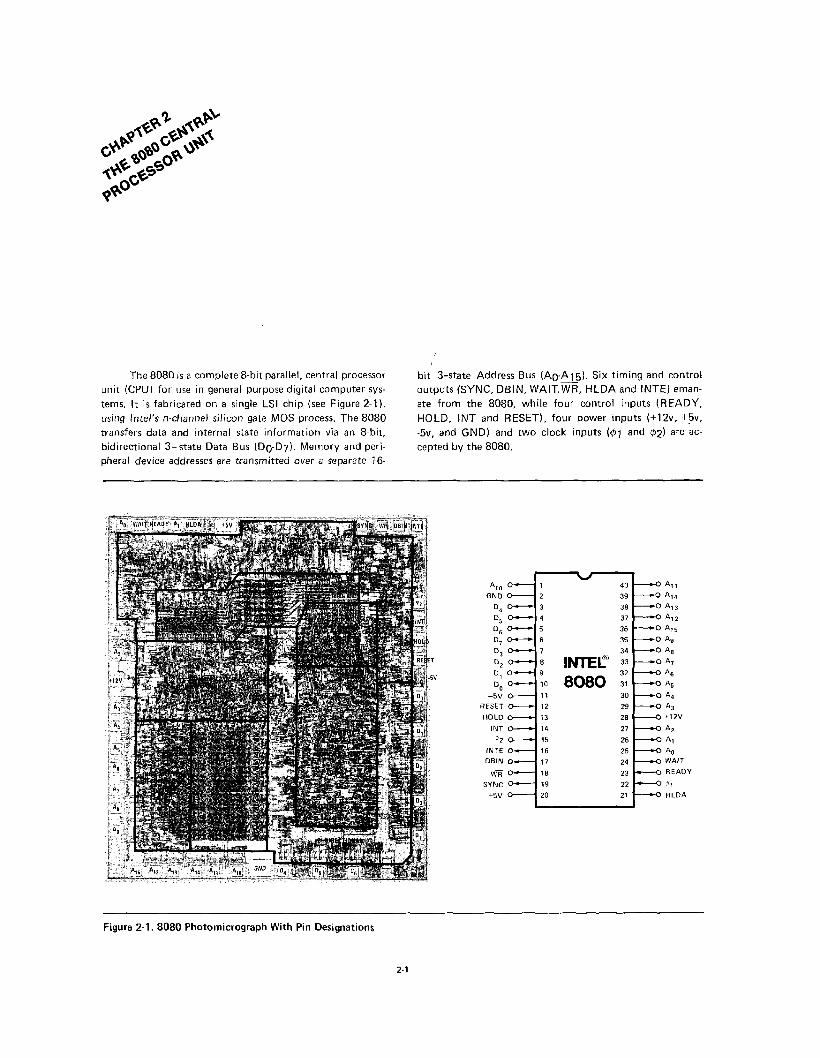
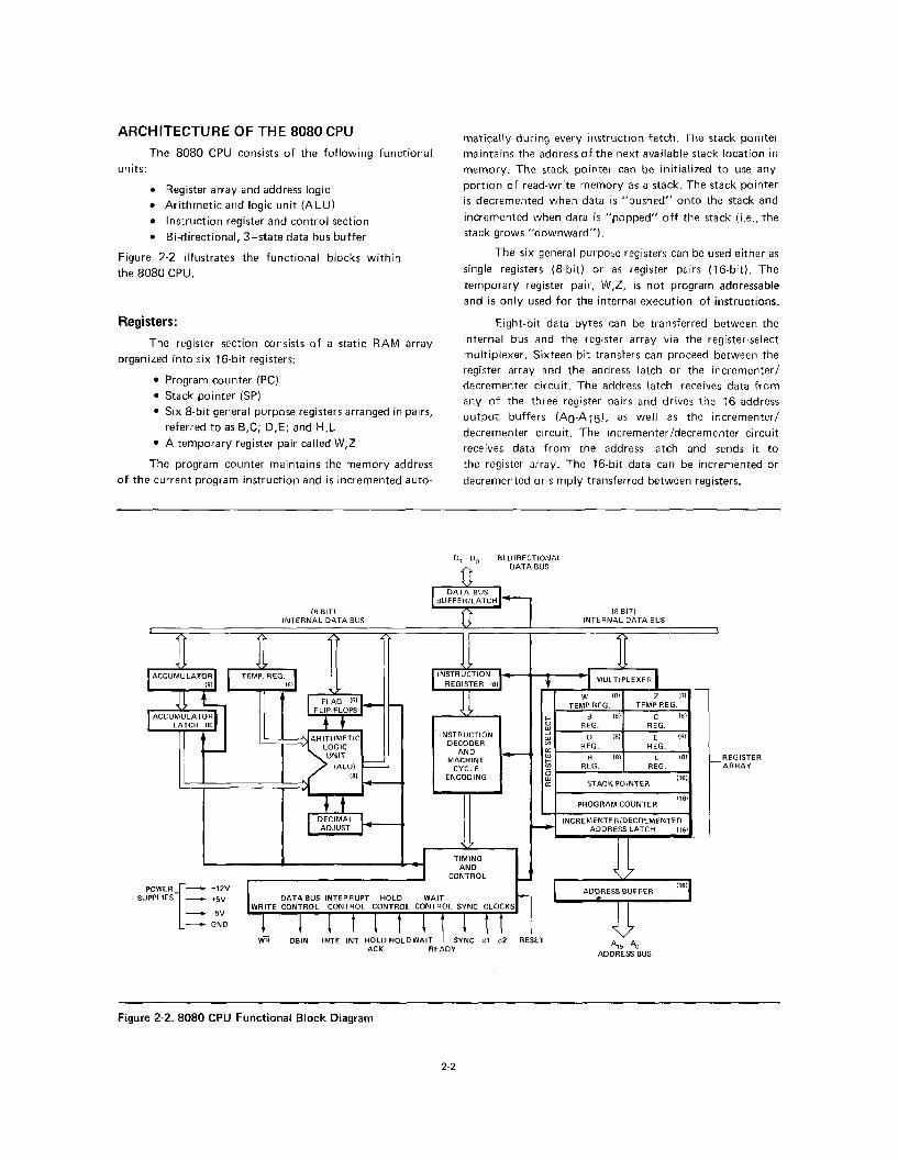
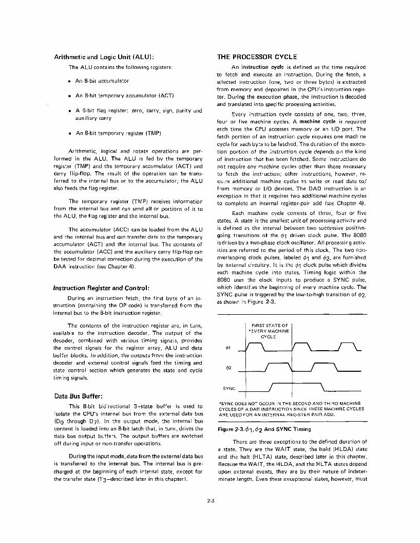
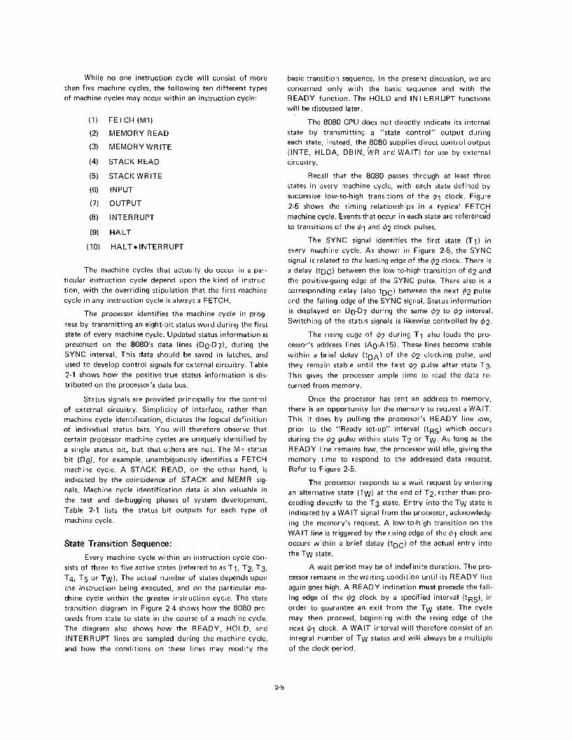
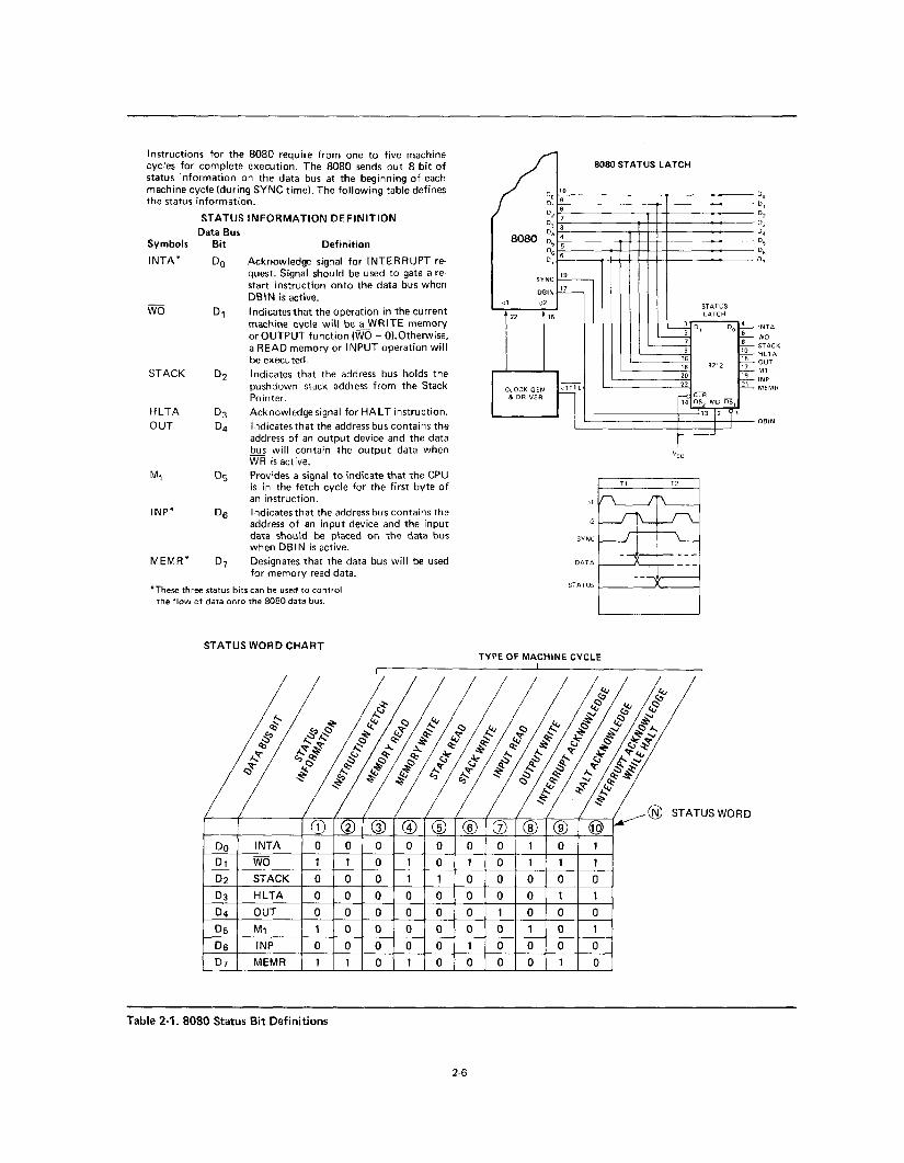
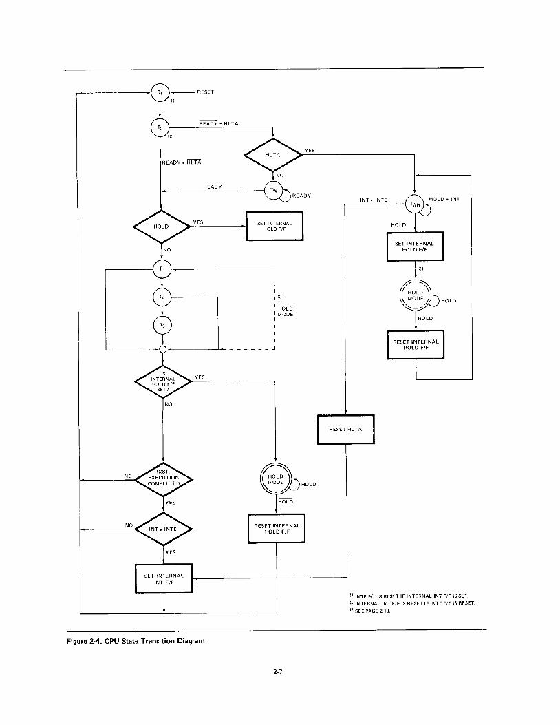
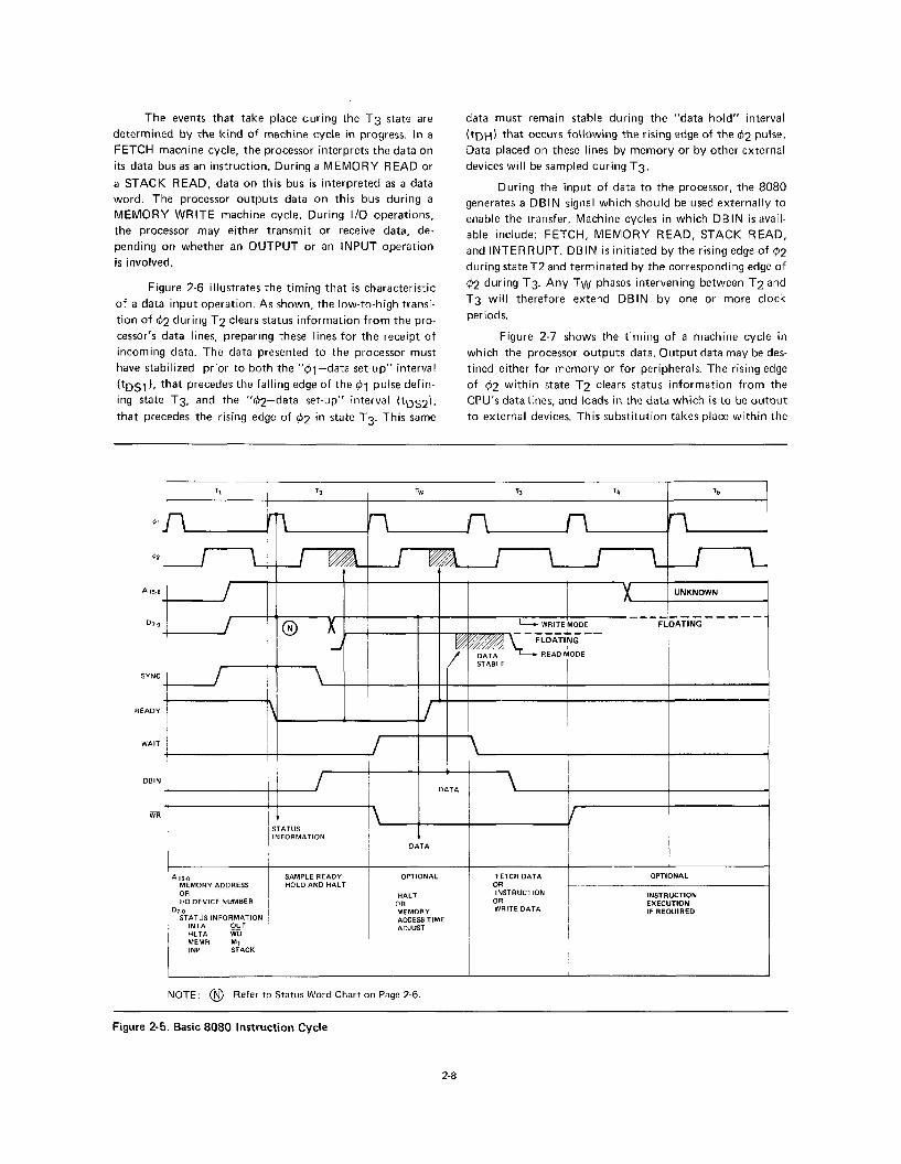
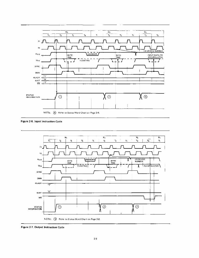
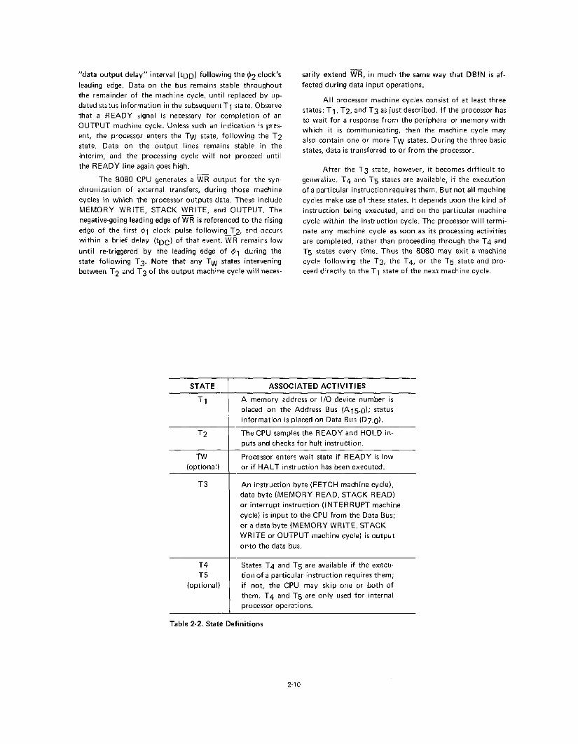
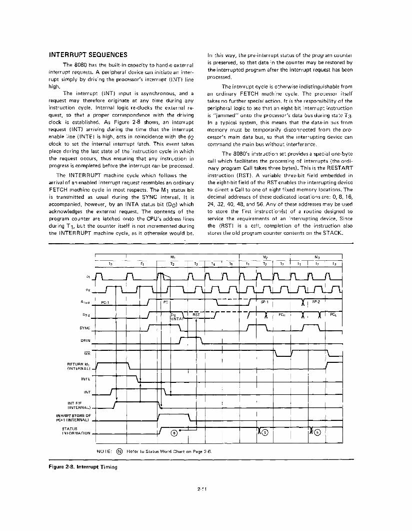
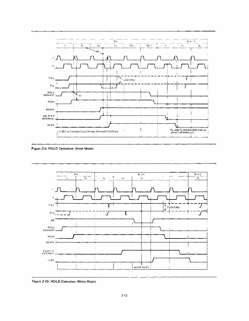
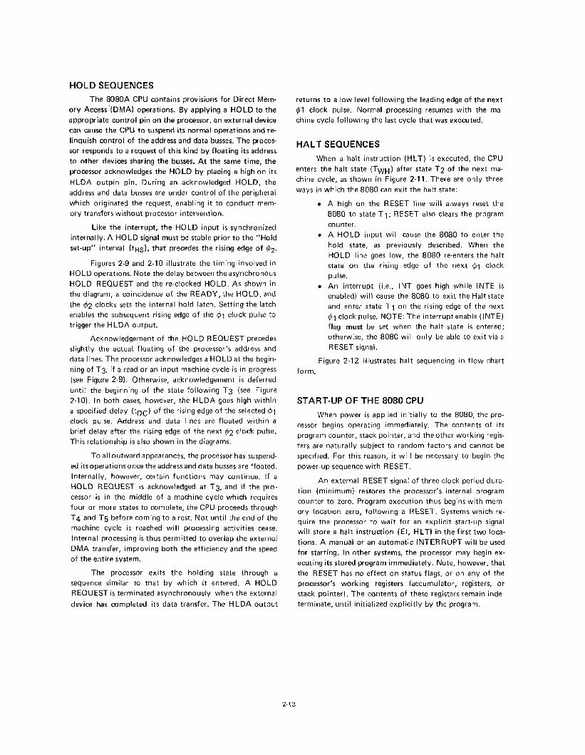
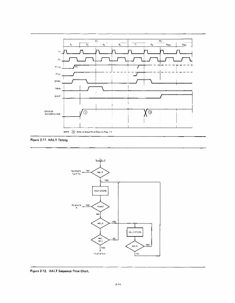
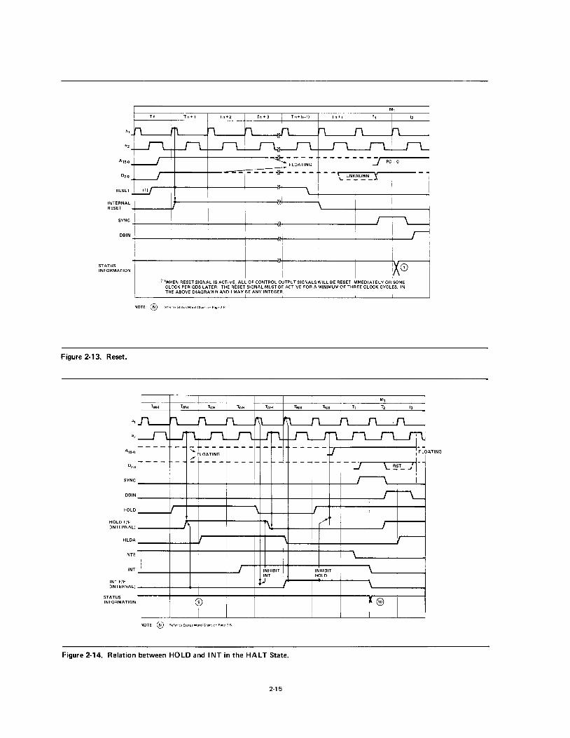
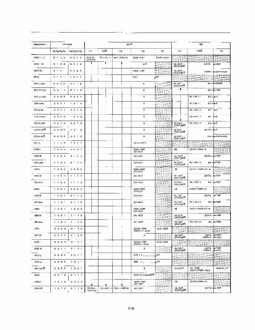
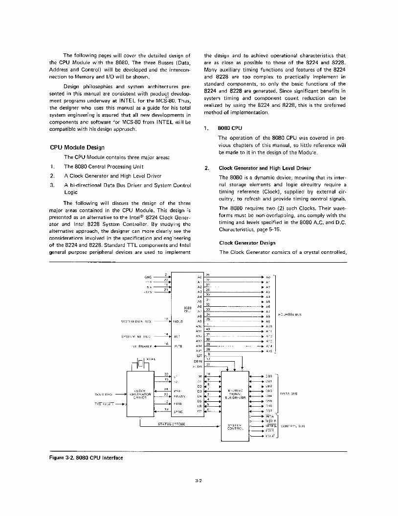
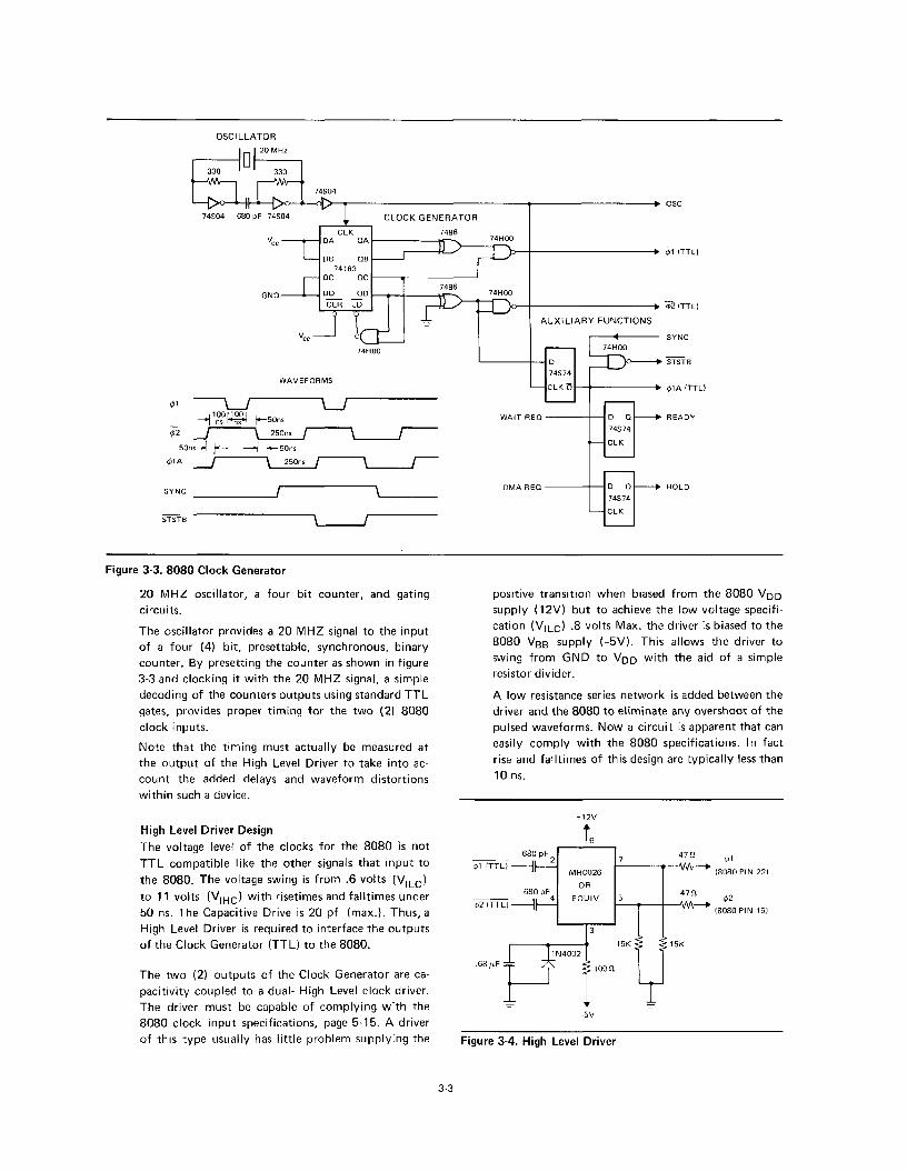
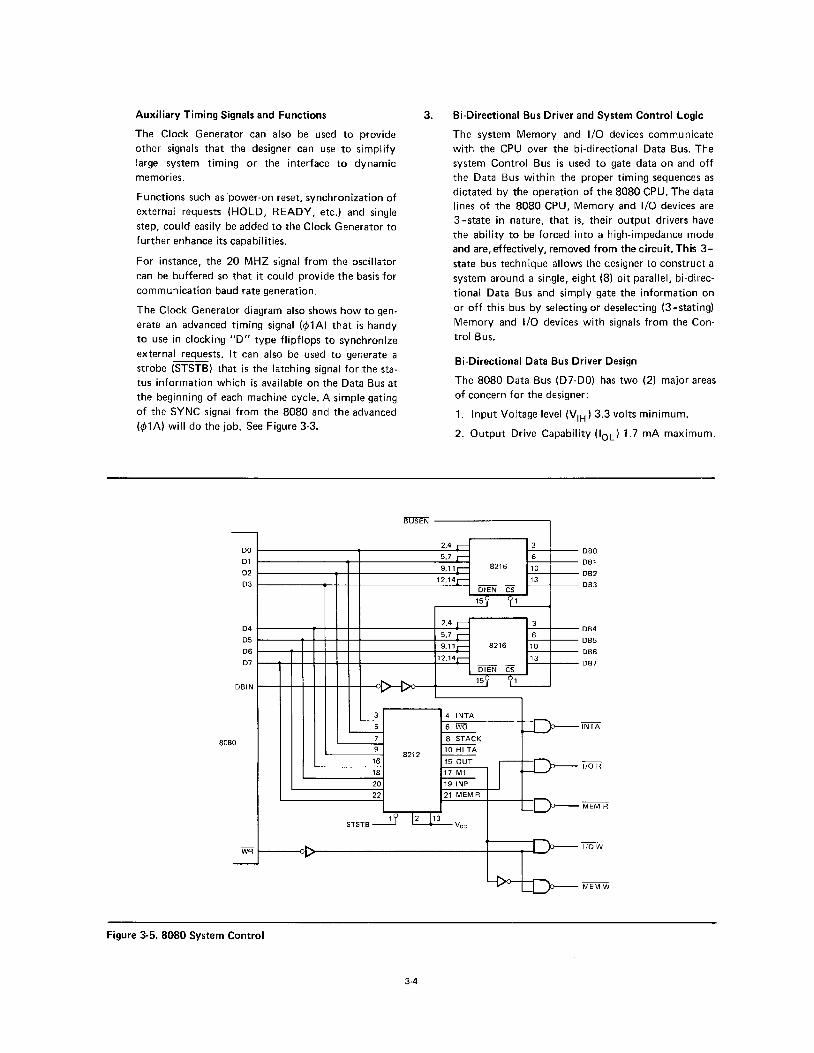
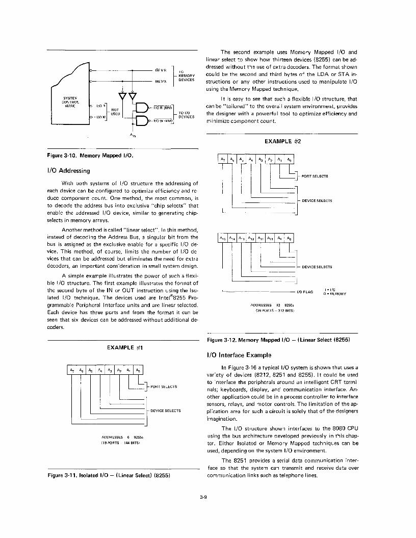
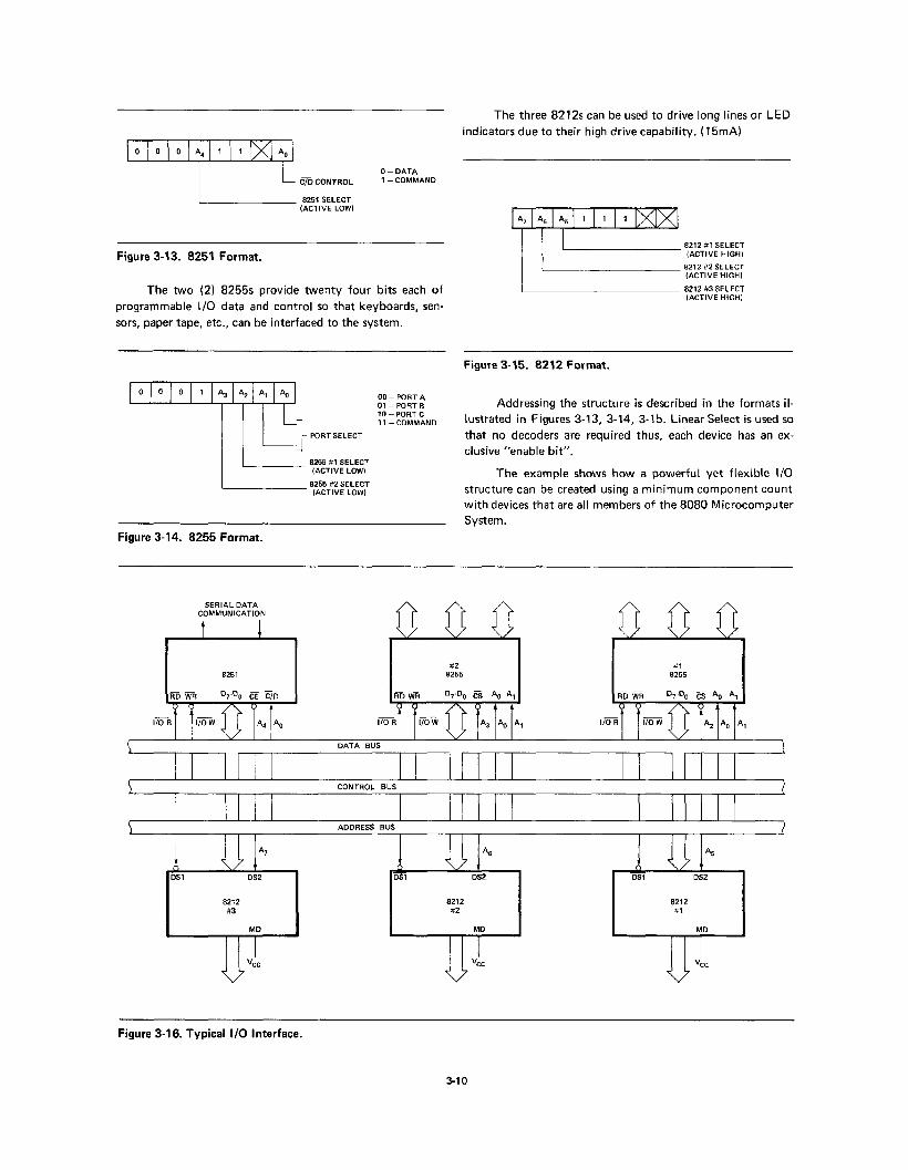
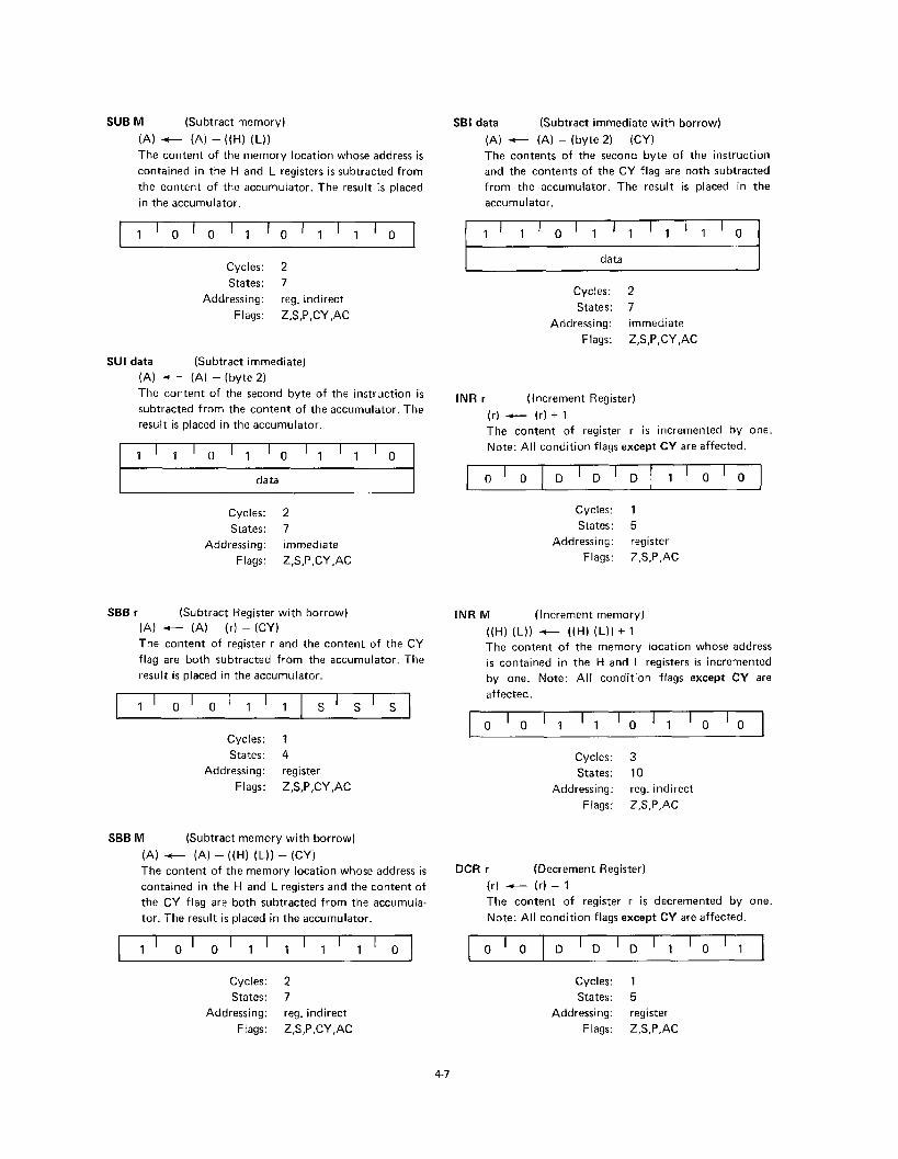
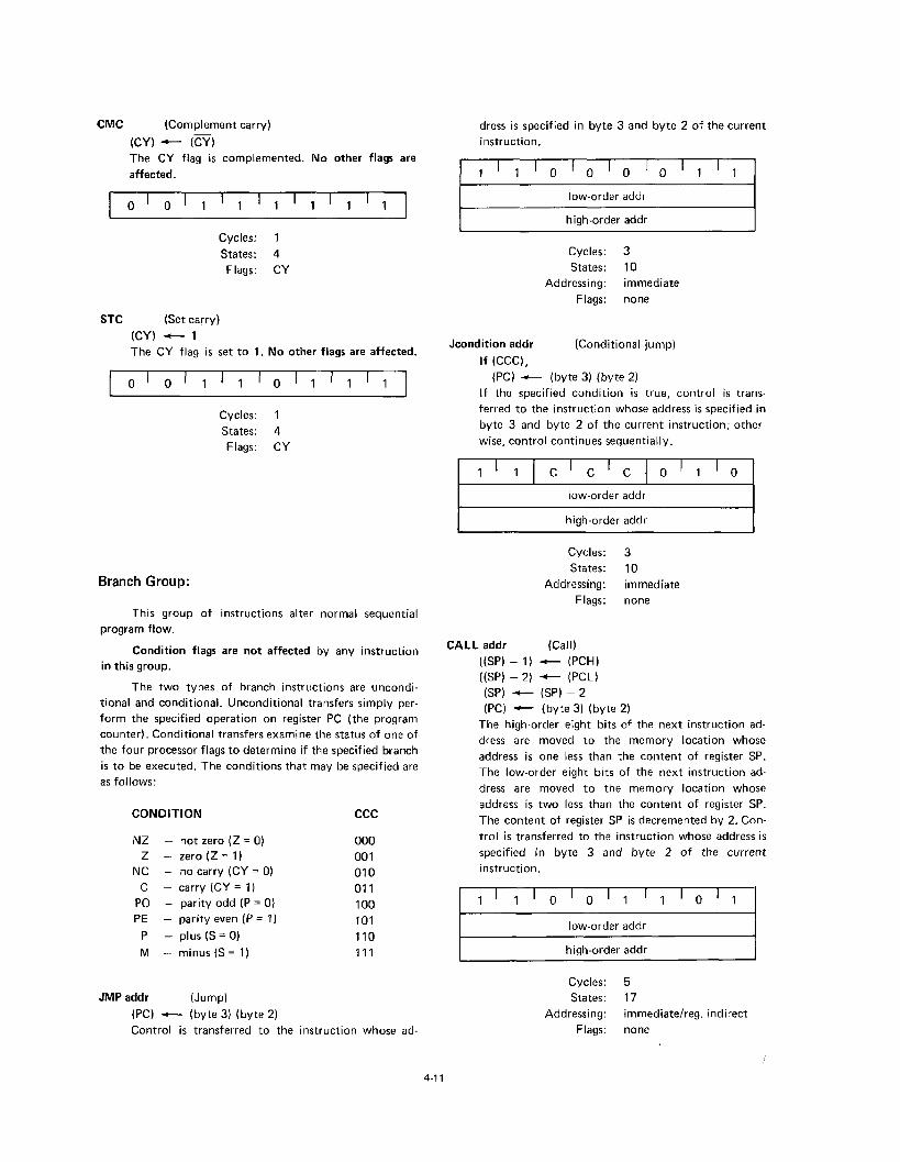
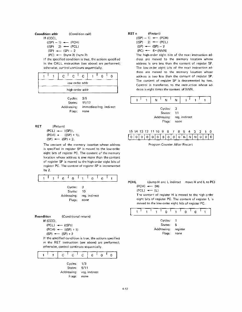
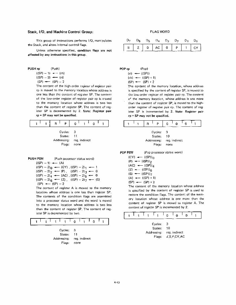

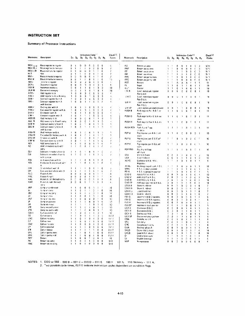
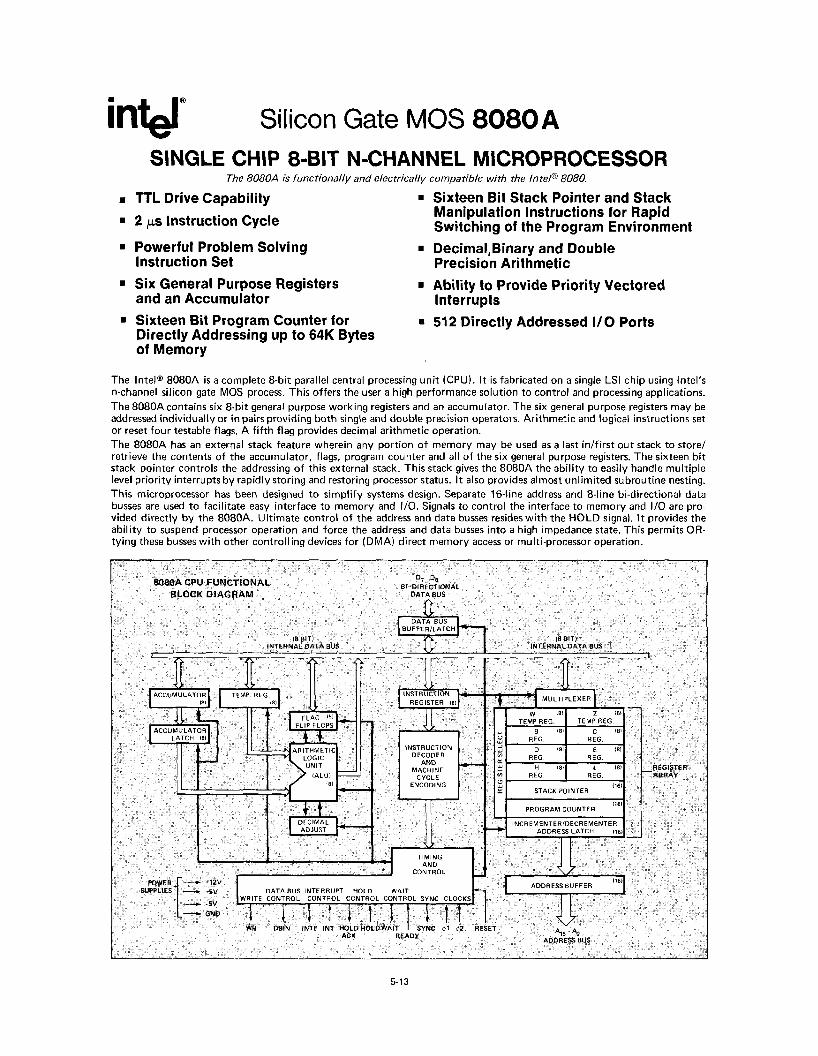
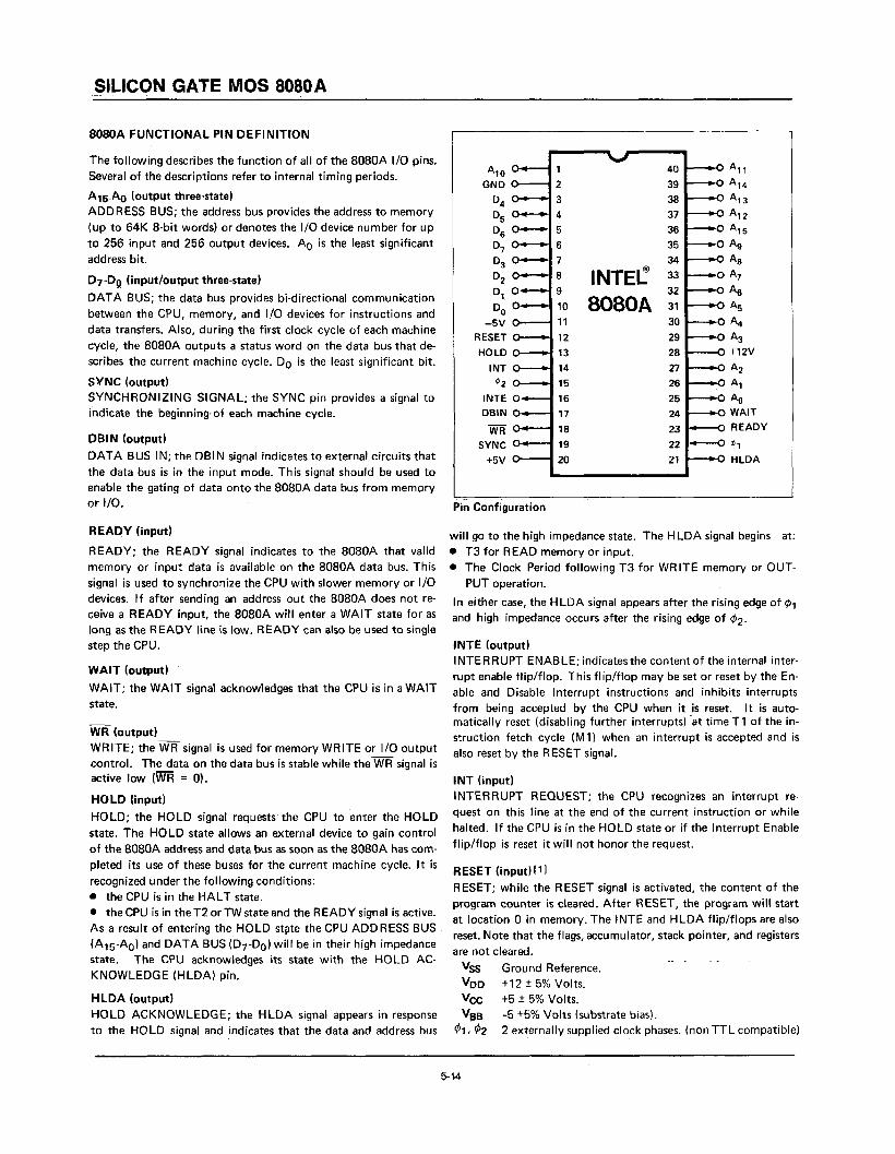
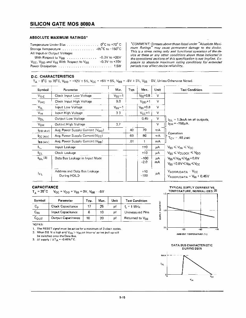
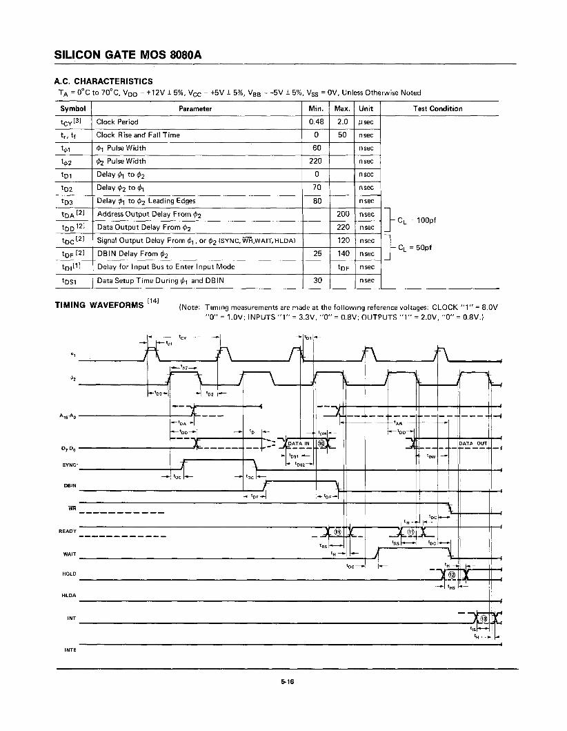
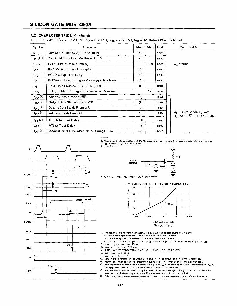
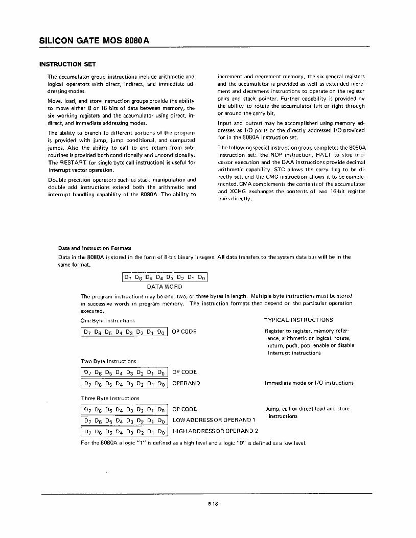
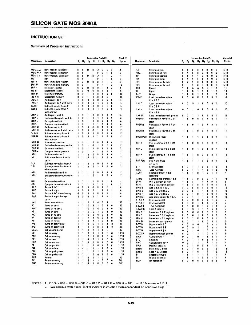
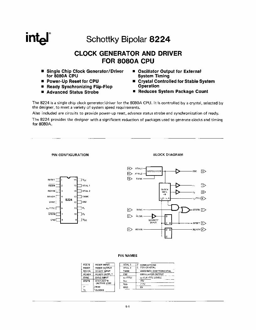
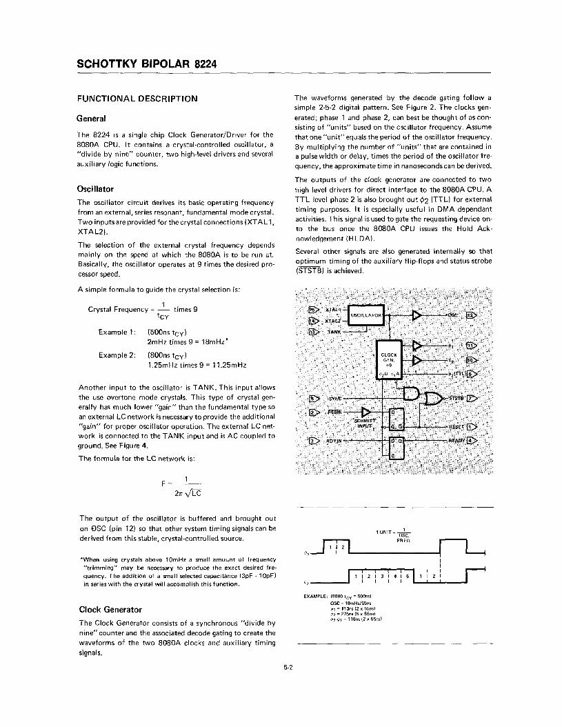
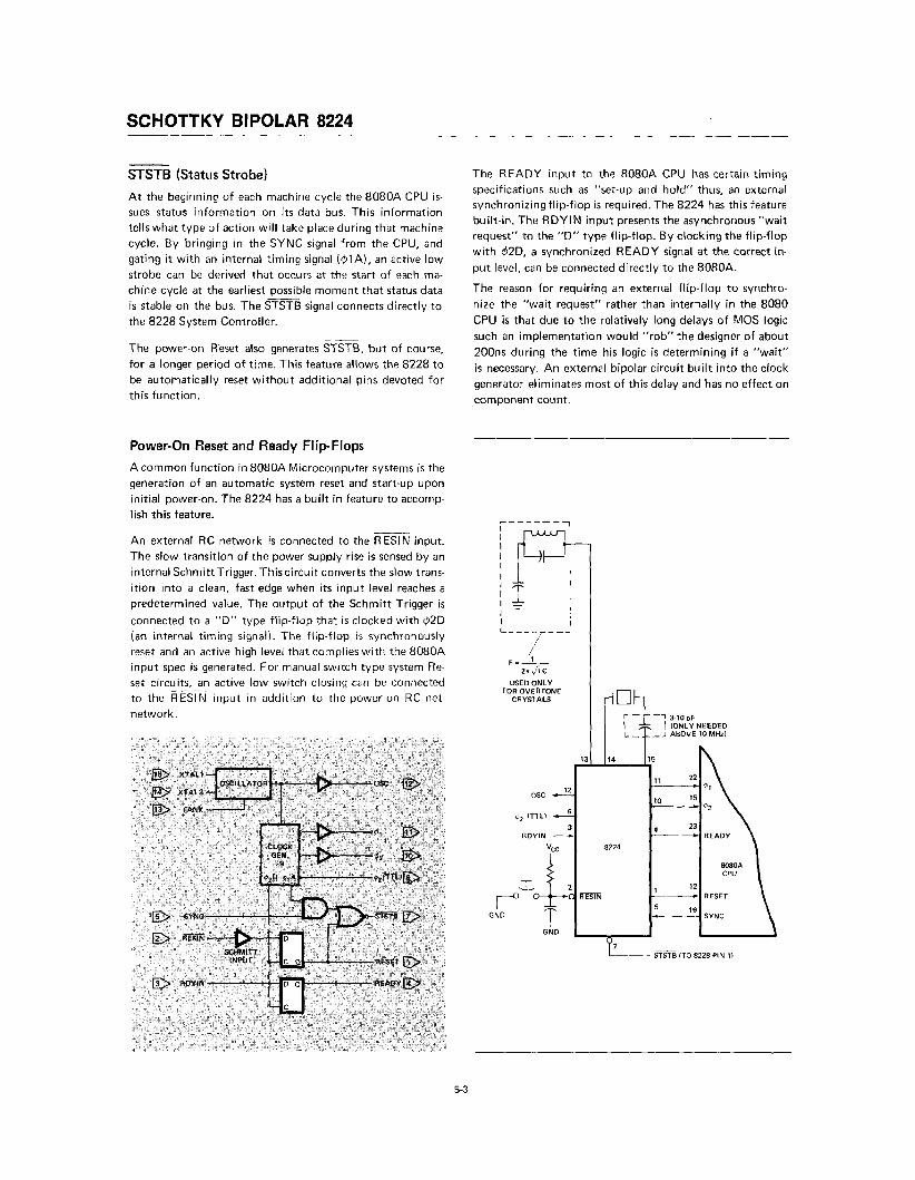
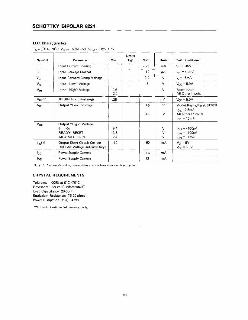
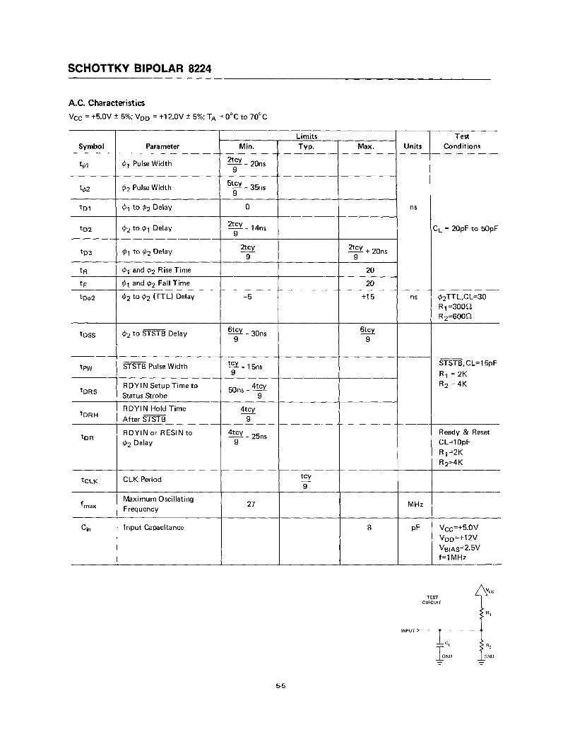
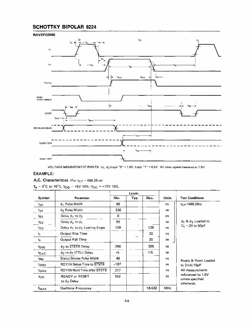
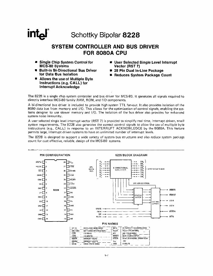
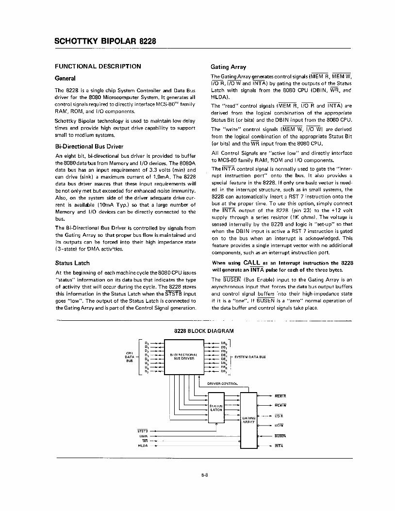
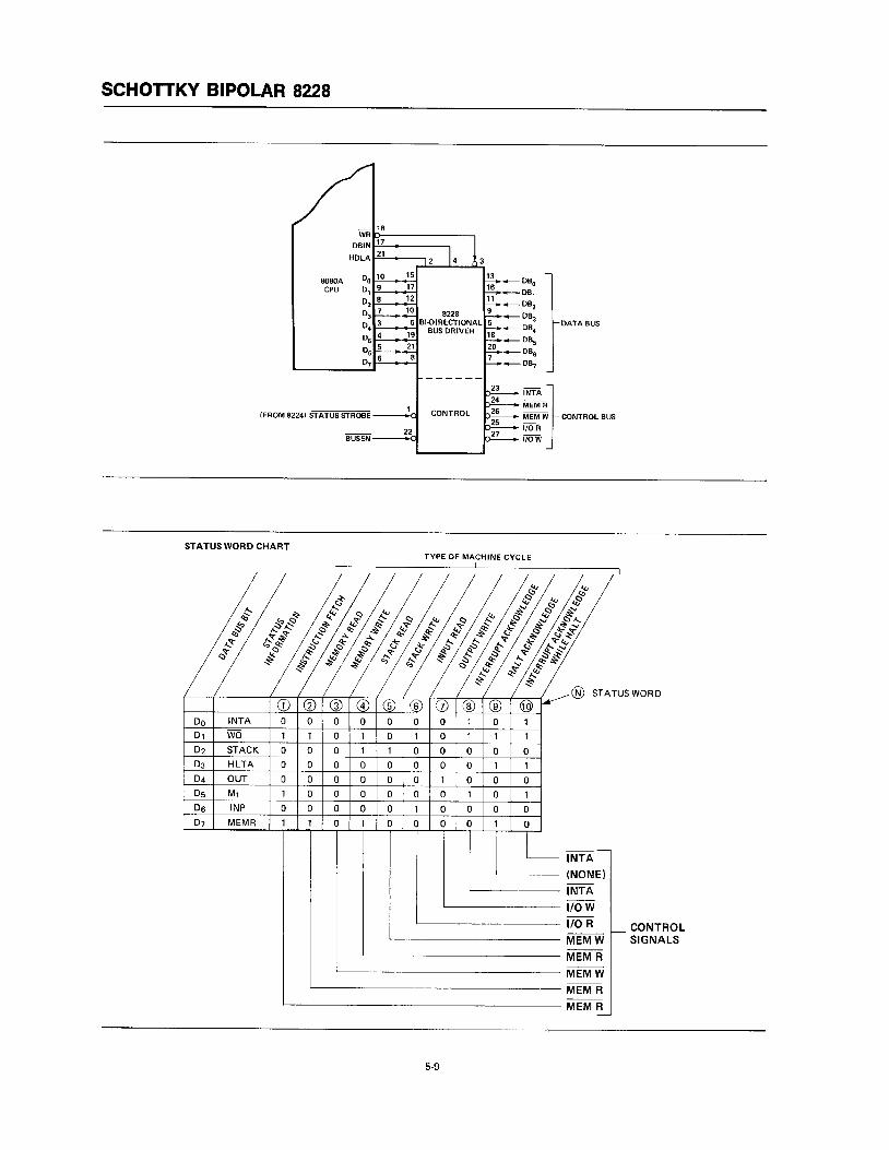
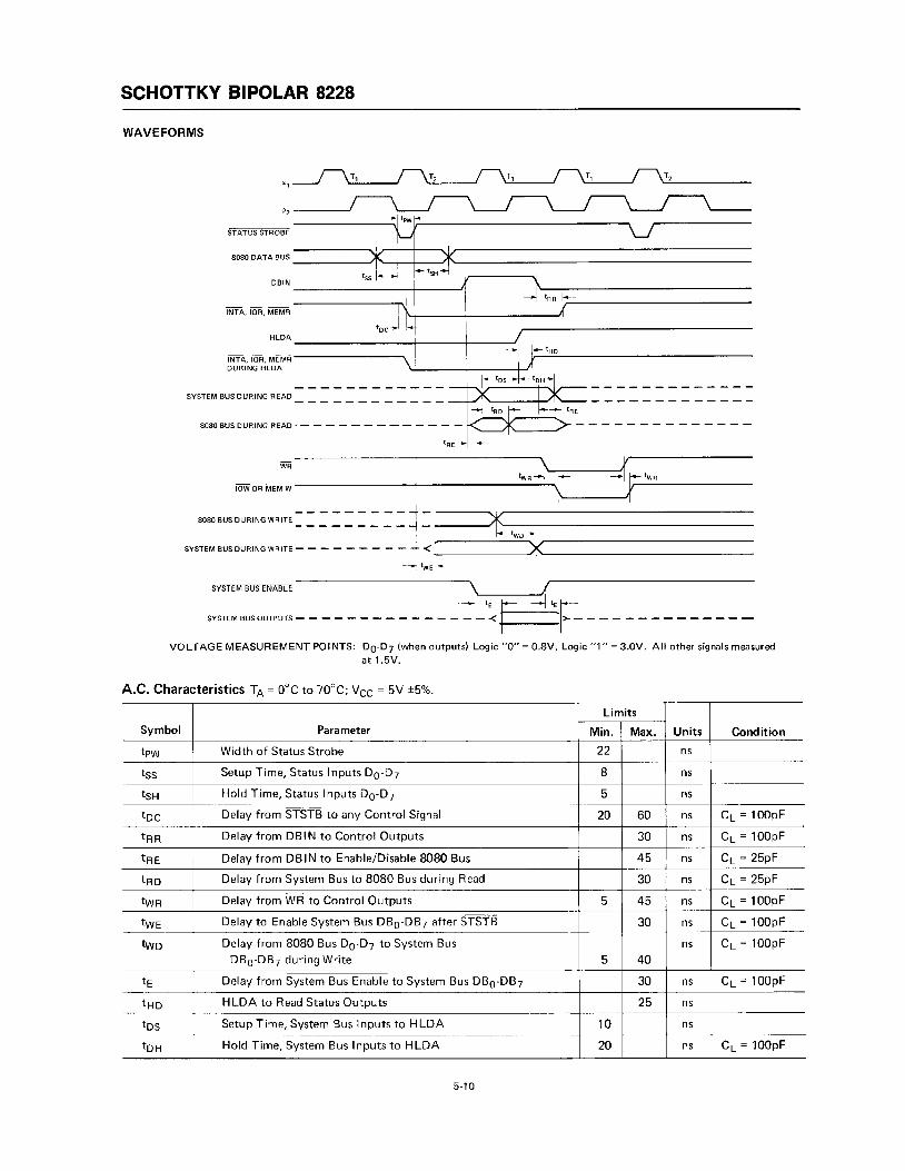
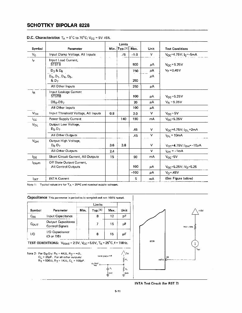
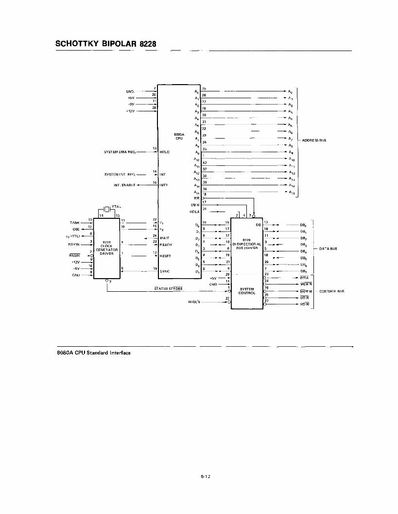


![INDEX [shodh.inflibnet.ac.in:8080]](https://static.documents.pub/doc/80x56/617729fad5903d63bd1810b7/index-shodh-.jpg)


![Index [182.160.97.198:8080]](https://static.documents.pub/doc/80x56/618107c6ef86d83c916e82c4/index-182160971988080.jpg)