This document contains information which is proprietary to CogniVue and may be used for non-commercial purposes within your organization in support of CogniVue’s products. No other use or transmission of all or any part of this document is permitted without written permission from CogniVue, and must include all copyright and other proprietary notices. Use or transmission of all or any part of this document in violation of any applicable Canadian or other legislation is hereby expressly prohibited.
User obtains no rights in the information or in any product, process, technology or trademark which it includes or describes, and is expressly prohibited from modifying the information or creating derivative works without the express written consent of CogniVue.
Disclaimer
CogniVue assumes no responsibility for the accuracy or completeness of the information presented which is subject to change without notice. In no event will CogniVue be liable for any direct, indirect, special, incidental or consequential damages, including lost profits, lost business or lost data, resulting from the use of or reliance upon the information, whether or not CogniVue has been advised of the possibility of such damages.
Mention of non-CogniVue products or services is for information purposes only and constitutes neither an endorsement nor a recommendation.
CV220X DataSheet
DS-10163-00-01
DS-10163-00-01 CogniVue Confidential and Proprietary
2/69
Revision History
Version Details of Change Author Date
01 Initial release Tina Jeffrey Dec 14, 2009
DS-10163-00-01 CogniVue Confidential and Proprietary
3/69
Table of Contents
1 Introduction.................................................................................................................................................. 8 1.1 CV220X Features .................................................................................................................................. 10
1.1.1 CV220X General Features............................................................................................................ 10 1.1.2 Video Processing .......................................................................................................................... 10 1.1.3 Digital Still Image Processing........................................................................................................ 11 1.1.4 Audio Processing .......................................................................................................................... 12 1.1.5 Graphics ........................................................................................................................................ 13 1.1.6 Image Sensor Interface................................................................................................................. 13 1.1.7 Display Controller .......................................................................................................................... 13 1.1.8 USB 2.0 HIGH SPEED Controller ................................................................................................. 13 1.1.9 Entropy Codec............................................................................................................................... 13 1.1.10 Integrated Memory ........................................................................................................................ 14 1.1.11 Audio Interface .............................................................................................................................. 14 1.1.12 Media Storage Interface................................................................................................................ 14 1.1.13 Serial Interfaces ............................................................................................................................ 14 1.1.14 MPEG-2 Transport Stream Interface ............................................................................................ 14 1.1.15 Smart Card Interface ..................................................................................................................... 14 1.1.16 Other Interfaces............................................................................................................................. 14
DS-10163-00-01 CogniVue Confidential and Proprietary
4/69
3.1.5 Display Interface Port and TV Output ........................................................................................... 27 3.1.6 MPEG2 Transport Interface (MP2TS)........................................................................................... 30 3.1.7 USB 2.0 HIGH SPEED.................................................................................................................. 31 3.1.8 Smart Card Interface ..................................................................................................................... 33 3.1.9 Serial Interfaces ............................................................................................................................ 34
5 Electrical Specifications............................................................................................................................. 60 5.1 Absolute Maximum Rating ..................................................................................................................... 60 5.2 Recommended Operating Ranges ........................................................................................................ 60 5.3 DC Characteristics ................................................................................................................................. 61 5.4 AC Specifications................................................................................................................................... 62
6 Ordering Information ................................................................................................................................. 69
DS-10163-00-01 CogniVue Confidential and Proprietary
DS-10163-00-01 CogniVue Confidential and Proprietary
8/69
1 Introduction The CV220X is a family of highly-programmable Image Cognition Processors (ICP) designed to enable programmable imaging and video applications for automotive smart cameras, internet protocol (IP) video surveillance cameras and converged consumer devices such as personal media players (PMP). CogniVue ICPs belonging to the CV220X family are programmable system-on-chip (SoC) devices powered by the APEX™ technology and include:
• CV2201 – Equipped with 128Mbit of stacked Mobile DDR SDRAM in package;
• CV2202 – Capable of interfacing to external DDR SDRAM up to 1Gbit in size;
• CV2203 – System in Package (SiP) with 1Gbit MLC NAND Flash and 128Mbit Mobile DDR SDRAM stacked in package; this device has variants qualified for industrial and automotive standards; automotive qualified parts conform to AEC-Q100;
These ICPs offer high performance programmable platform solutions while providing developers with a low power, extremely flexible device for full-featured imaging and video applications including mobile TV for converged applications such as personal media players (PMPs) and imaging and video analytics for use in smart cameras for ensuring driver safety and enhancing security. These target applications may benefit from the following feature set:
• All video codec standards support D1 resolution at 30fps (see Section 1.1.2 for details)
• Video/audio player with dual MPEG2 Transport Stream interfaces supporting DVB-H/T and ATSC-M/H channels for picture-in-picture
• Digital still image capture supporting sensors up to 12 Mpixels
• TV output (NTSC/PAL) via cable or Bluetooth with TV encoder DAC on chip
• Support for all new algorithms (proprietary or standard) with software changes only
• Picture viewer with image editing options
• Video editing, VOD, Video-Telephony (VT), Multimedia Messaging Service (MMS)
• WM-DRM, OMA-DRM, DivX-DRM ready
• Support for compute-intensive multi-tasking operations such as handling video ring tone while watching DVB-H/T PIP
• Video editing
• Transcoding
• Integrated security and cryptographic support features for digital rights, content protection and subscription services
• Multiple power domains allow for low power operation
DS-10163-00-01 CogniVue Confidential and Proprietary
9/69
• USB 2.0 High Speed interface including PHY on chip
• SD/SDHC, MMC Plus and NAND flash interface
• Small form factor for stacked or external memory
Figure 1 shows a typical configuration of the CV220X ICP.
DAC/ADC
S/T-DMB/DVB-H Baseband
1 77
77 7
7 0
88 Joh
n D
oe
Stacked or ExternalNAND Flash
SD/SDHC and
MMC Plus
CMOS/CCD YUV 8-bit
Quad Buffer LCDs8/16/18-bit
or VGA RGB LCD
AnalogNTSC/PAL
USB Device
(e.g. PC)
Keypad
Figure 1: CV220X Based Personal Media Player/Recorder
DS-10163-00-01 CogniVue Confidential and Proprietary
10/69
1.1 CV220X Features
1.1.1 CV220X General Features
• Dual ARM926EJ-S™ RISC processor each with 16 kB I-cache and 16 kB D-cache
• High performance APEX™ DSP Sub-System technology based on patented SIMD parallel processing architecture
• Integrated Jazelle Java hardware accelerator
• Integrated USB 2.0 High Speed Controller
• Sensor Interface supports 10-bit YUV datapath providing up to 12 Mpixel resolution
• Integrated image enhancement functions in Sensor Interface
• Dual MP2TS interfaces for use with mobile TV applications
• Multiple power domains and voltage islands to support low power modes
• DMA Controller for memory-to-memory, memory-to-peripheral, peripheral-to-memory, and peripheral-to-peripheral data transfer
• Digital output supporting up to 24 bits with external video DAC
• Integrated 10-bit DAC for analog composite video output to TV
• Dual LCD module
• Data security and pay-per-view features:
• Hardware acceleration for OMA-2 cryptographic operations
• Secure boot mode
• Smart Card Interface
• SD/SDHC Interface
• MMC Plus Interface
• NAND Flash Interface
1.1.2 Video Processing
• Fully-programmable Array Processor for running video processing algorithms
• Video codecs support diverse resolutions at 30fps with 4 Mbps maximum bitrate
• Supports wide cam (768 x 432) encoding at 30fps
DS-10163-00-01 CogniVue Confidential and Proprietary
11/69
• Supports slow motion (eg. 1/5th at 30fps)
• Supported video decoding standards:
• MPEG-4 Simple Profile and Advanced Simple Profile supports D1 at 30fps
• H.263 Baseline, Profile 3 supports D1 at 30fps
• DivX (v5.0/6.0) with DRM supports D1 at 30fps
• XviD supports D1 at 30fps
• MPEG2 support D1 at 30fps
• WMV (VC-1) with DRM supports D1 at 30fps
• H.264 supports D1 at 30fps
• RV supports D1 at 30fps
• RMVB supports D1 at 30fps
• VP6 supports D1 at 30fps
• Supported video encoding standards:
• MPEG-4 Simple Profile supports D1 at 30fps or QVGA at 120fps
• H.263 Baseline Profile supports D1 at 30fps
• DiVX/XViD avi support D1 at 30fps
• All new codec standards may be supported with SW change only
• Supports video streaming and progressive download
• Supports full motion estimation and variable pixel search region
• Supports constant and variable bit rate (CBR and VBR)
• Real-time viewfinder on LCD and TV with scaling, rotation, mirroring and flipping transformations
• Supports special effects: black and white, sepia, negative, cool, hot, sketch, emboss and others
1.1.3 Digital Still Image Processing
• Captures still images up to 12 Mpixels using image sensor with ISP
• Supports image processing and editing
• Compression and decompression in accordance with ISO/IEC 10918 JPEG standard
DS-10163-00-01 CogniVue Confidential and Proprietary
12/69
• Supports JPEG capture on-the-fly
• Support for common decompression standards: TIFF, GIF, PNG and WBMP
• Supports Exchangeable Image File (EXIF) format
• Programmable quantization and Huffman tables and high, medium and low compression quality settings
• Real-time viewfinder on LCD and TV with scaling, rotation, mirroring and flipping transformations
• Supports special effects: B&W, sepia, negative, cool, hot, sketch, emboss and others
• Image scaling and window of interest
• Supports continuous digital zoom (including true upscaling) up to 2X
• Supports decorative frame overlay and photo captioning
• Thumbnail browser and file management
1.1.4 Audio Processing
• Audio encoding compliant with the following standards: AAC, MP3, AMR-NB, G.723.1, WAV
• Audio decoding compliant with the following standards: AAC, AAC+, EAAC+, MP3, BSAC, WMA, WMA10 Pro, RA, AMR-NB, AMR-WB, G.723.1, WAV, OGG
• Supports MTP and music player DB
• All other codec standards may be supported with SW change only
• MIDI synthesis of up to 128 voices at 48 kHz for Melody Ring Tones supporting wide range of MIDI files including:
• .mid MIDI file format
• .rtx extended ringtone format
• .sms SMS ringtone
• .xmf extensible music format (MIDI + digitally recorded music)
• .mxmf mobile version of .xmf
• .mmf SMAF ringtone format
• .rmf rich music format
• .imy iMelody ringtone format
DS-10163-00-01 CogniVue Confidential and Proprietary
13/69
• Directly connects to I2S or AC97 compliant audio device
• Supports up to four CPU-like devices (for example dual 8/9/16/18-bit LCD modules and two other devices with CPU-like interfaces) concurrently with TV Out, or support RGB-24 master timing interface up to XGA resolution
• ITU-R 601/656 compatible digital video output
• On-chip composite video encoder compatible with PAL/NTSC/NTSC-Japan video modulation standards
• Integrated high quality 10-bit video DAC for direct connection to TV
• Embedded Bit Packing and Unpacking Blocks for automated file/video stream generation
• Direct connection with Array Processor for efficient data transfer
DS-10163-00-01 CogniVue Confidential and Proprietary
14/69
1.1.10 Integrated Memory
• CV2201 has 128 Mbit DDR SDRAM integrated in package
• CV2202 has no internal memory but is capable of interfacing to external SDRAM up to 1Gbit in size
• CV2203 has 128 Mbit DDR SDRAM and 1Gbit NAND flash integrated in package
1.1.11 Audio Interface
• I2S and AC97 compliant Audio Interface
1.1.12 Media Storage Interface
• Supports SD/SDHC removable memory cards
• Supports MMC Plus memory card
• Supports 8-bit NAND flash devices
• Supports FAT-16 and FAT-32 file system with long name support and international characters
1.1.13 Serial Interfaces
• Two UART interfaces and two SPIs
1.1.14 MPEG-2 Transport Stream Interface
• Dual interfaces to DMB baseband to receive MPEG2 transport streams
1.1.15 Smart Card Interface
• Complies with integrated circuit card specifications: ISO/IEC 7816-3 amendment I (2002-06-01); ISO/IEC 7816-10; EMV Book 1 Version 4.1 (2004-05-01)
1.1.16 Other Interfaces
• General purpose I/O (GPIO) – selectable as alternative functions for various interface pins
• Two PWM (Pulse width modulated) outputs with programmable frequency and duty cycle
• JTAG test and debugging interface for ARMs
DS-10163-00-01 CogniVue Confidential and Proprietary
15/69
1.2 Reference Input Clock
• Programmable internal clock frequencies
• Input clocks:
• 10-30 MHz
• 5 on-chip PLLs generate clocks for system, array processor, display interface, other interfaces and memory
• Clocks supplied by either a crystal or oscillator
1.3 Boot-Up Options
• Code resident in NAND flash accessible via SPI or NAND interface
1.4 Package
• CV2201 is available in a 9 x 9mm BGA package, with 236 balls
• CV2202 is available in a 10 x 10mm BGA package with 296 balls
• CV2203 is available in a 10 x 10 mm BGA package, with 196 balls
1.5 Power Supply
• 1.0 V core and 1.8/2.8 V I/O power
• 1.8V memory power supply
• 3.0 V PLL power supply
• 3.3 V supplies for USB and internal DAC
• Multiple power domain within the core for power management
1.6 Ambient Operating Temperature
• CV2201 and CV2202 operate between -40°C to +85°C
• CV2203 industrial qualified parts operate between -40°C to +85°C; CV2203 automotive qualified parts operate between -40°C to +125°C
DS-10163-00-01 CogniVue Confidential and Proprietary
16/69
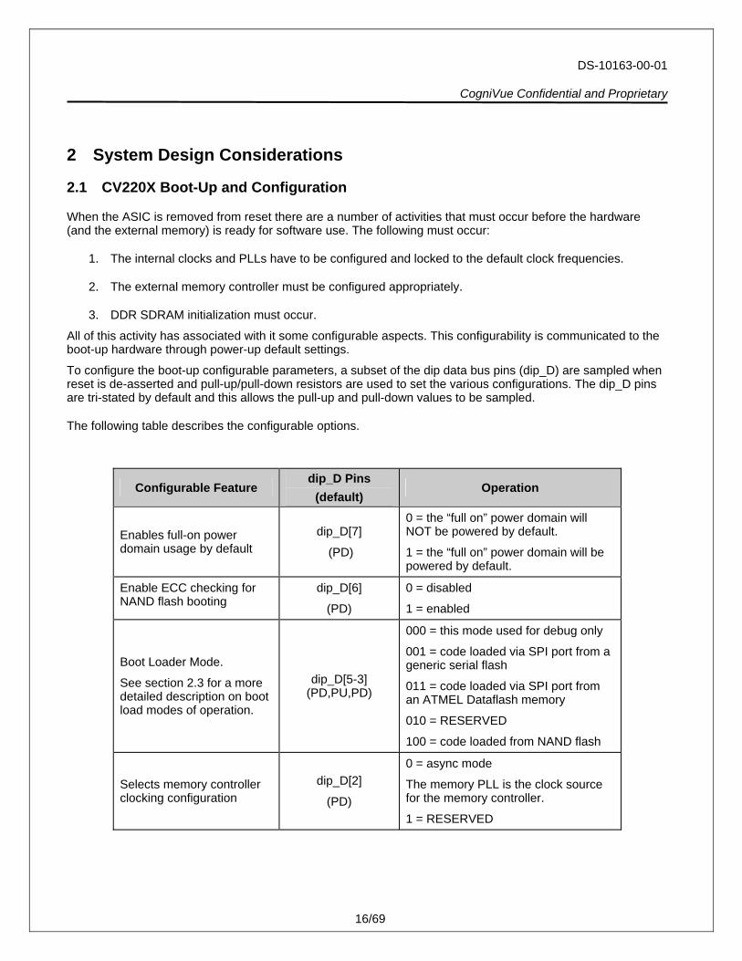
2 System Design Considerations
2.1 CV220X Boot-Up and Configuration
When the ASIC is removed from reset there are a number of activities that must occur before the hardware (and the external memory) is ready for software use. The following must occur:
1. The internal clocks and PLLs have to be configured and locked to the default clock frequencies.
2. The external memory controller must be configured appropriately.
3. DDR SDRAM initialization must occur.
All of this activity has associated with it some configurable aspects. This configurability is communicated to the boot-up hardware through power-up default settings.
To configure the boot-up configurable parameters, a subset of the dip data bus pins (dip_D) are sampled when reset is de-asserted and pull-up/pull-down resistors are used to set the various configurations. The dip_D pins are tri-stated by default and this allows the pull-up and pull-down values to be sampled.
The following table describes the configurable options.
Configurable Feature dip_D Pins
(default) Operation
Enables full-on power domain usage by default
dip_D[7]
(PD)
0 = the “full on” power domain will NOT be powered by default.
1 = the “full on” power domain will be powered by default.
Enable ECC checking for NAND flash booting
dip_D[6]
(PD)
0 = disabled
1 = enabled
Boot Loader Mode.
See section 2.3 for a more detailed description on boot load modes of operation.
dip_D[5-3] (PD,PU,PD)
000 = this mode used for debug only
001 = code loaded via SPI port from a generic serial flash
011 = code loaded via SPI port from an ATMEL Dataflash memory
010 = RESERVED
100 = code loaded from NAND flash
Selects memory controller clocking configuration
dip_D[2]
(PD)
0 = async mode
The memory PLL is the clock source for the memory controller.
1 = RESERVED
DS-10163-00-01 CogniVue Confidential and Proprietary
17/69
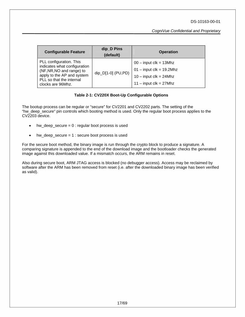
Configurable Feature dip_D Pins
(default) Operation
PLL configuration. This indicates what configuration (NF,NR,NO and range) to apply to the AP and system PLL so that the internal clocks are 96Mhz.
dip_D[1-0] (PU,PD)
00 – input clk = 13Mhz
01 – input clk = 19.2Mhz
10 – input clk = 24Mhz
11 – input clk = 27Mhz
Table 2-1: CV220X Boot-Up Configurable Options
The bootup process can be regular or “secure” for CV2201 and CV2202 parts. The setting of the “hw_deep_secure” pin controls which booting method is used. Only the regular boot process applies to the CV2203 device.
• hw_deep_secure = 0 : regular boot process is used
• hw_deep_secure = 1 : secure boot process is used
For the secure boot method, the binary image is run through the crypto block to produce a signature. A comparing signature is appended to the end of the download image and the bootloader checks the generated image against this downloaded value. If a mismatch occurs, the ARM remains in reset.
Also during secure boot, ARM JTAG access is blocked (no debugger access). Access may be reclaimed by software after the ARM has been removed from reset (i.e. after the downloaded binary image has been verified as valid).
DS-10163-00-01 CogniVue Confidential and Proprietary
18/69
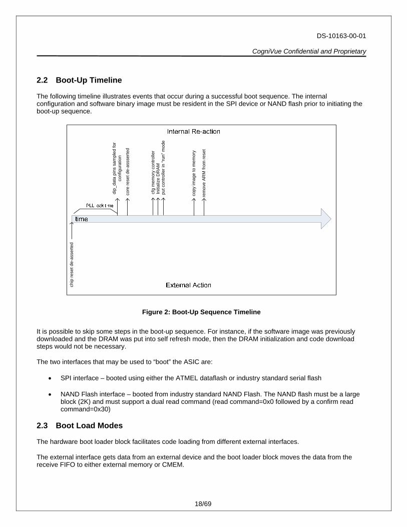
2.2 Boot-Up Timeline
The following timeline illustrates events that occur during a successful boot sequence. The internal configuration and software binary image must be resident in the SPI device or NAND flash prior to initiating the boot-up sequence.
chip
rese
t de-
asse
rted
dip_
data
pin
s sa
mpl
ed fo
r co
nfig
urat
ion
core
rese
t de-
asss
erte
d
cfg
mem
ory
cont
rolle
rIn
itial
ize
DR
AM
put c
ontro
ller i
n “r
un” m
ode
copy
imag
e to
mem
ory
rem
ove
ARM
from
rese
t
Figure 2: Boot-Up Sequence Timeline
It is possible to skip some steps in the boot-up sequence. For instance, if the software image was previously downloaded and the DRAM was put into self refresh mode, then the DRAM initialization and code download steps would not be necessary.
The two interfaces that may be used to “boot” the ASIC are:
• SPI interface – booted using either the ATMEL dataflash or industry standard serial flash
• NAND Flash interface – booted from industry standard NAND Flash. The NAND flash must be a large block (2K) and must support a dual read command (read command=0x0 followed by a confirm read command=0x30)
2.3 Boot Load Modes
The hardware boot loader block facilitates code loading from different external interfaces.
The external interface gets data from an external device and the boot loader block moves the data from the receive FIFO to either external memory or CMEM.
DS-10163-00-01 CogniVue Confidential and Proprietary
19/69
While the Boot Loader is operating, the ARM is held in reset so that it does not start executing code until the complete program store is in place. When the byte counter expires, indicating all code has been copied, the boot loader indicates to the reset block that the ARM can be removed from reset.
Possible boot loader configurations, as specified by the downloaded configuration information, are identified in the table below.
dip_data[5:3] Description
000 This setting will not invoke the boot loader and the ARM will be removed from reset immediately. This is a debug mode of operation. Code must be written to memory through some other means (ie. JTAG Port).
011 Code is resident in a serial NAND flash connected to the SPI port. The serial Flash Memory is an ATMEL DataFlash memory that supports the “continuous array read” command (0xe8).
001 Code is resident in a serial NAND flash connected to the SPI port. The serial Flash Memory is an industry standard memory that supports the “read data bytes” command (0x03).
010 THIS SETTING IS RESERVED AND SHOULD NOT BE USED.;
100
Code is resident in NAND flash. The NAND flash block read sequence is:
a. After reset is de-asserted, the bootloader will issue a “reset” command (“FF”) followed by a 25 usec delay.
b. The boot loader then issues the page read command (“00”) and 5 bytes of address (all “0”). This is followed by a read confirm command (“30”).
c. Before proceeding further, a 50usec delay occurs.
d. A 2Kbyte page is then read. If ECC is enabled four 512byte page reads are issued.
Table 2-2: Configuring Boot Load Using dip_data[5:3] Pins
If booting from NAND Flash, there is an optional ECC checking mode that may be enabled via a software register. If ECC checking is enabled, the boot_loader checks for errors after a block is read from the device. Upon error detection, the boot loader keeps the ARM in reset.
2.4 Low Power Configurations
Some system operating modes require limited CV220X functionality in which case the ICP may operate in a low power mode. The CV220X is comprised of multiple voltage islands that enable various low power configuration scenarios. The voltage islands are intended to be activated in a cumulative manner based on the particular functionality required. The power configurations are listed below. The list is organized with the least functionality and power first, followed by increasing functionality and power.
1. Low Power Audio/Video – This mode adds to the low power passthrough mode appropriate circuitry for low power MP3 decoding as well as some display functionality.
2. Full-on Power – This mode activates the rest of the CV220X functionality.
DS-10163-00-01 CogniVue Confidential and Proprietary
20/69
The low power mode is achieved by disconnecting the core power. This mode removes any power drain associated with core leakage.
In addition to the modes listed above, the CV220X is designed in such a way that each block may individually have its clock gated under software control. This provides a mechanism to lower power consumption for an application that does not require functionality from all blocks. Also many of the blocks have a hardware controlled mechanism that allows each block to gate its own clock when it is idle and remove the clock gating when activity resumes. This mechanism may be disabled by software if desired.
2.5 Reset
The internal reset architecture is controlled by an external reset pin and also by software initiated reset requests.
The external reset pin, when asserted, keeps the entire chip in a reset state. After the power supply voltages have stabilized, the external reset must remain asserted for 1 μsec. After the external reset is removed, the timing generation block is removed from reset and starts a timer to time the PLL lock interval. The timing generation block keeps the rest of the chip in reset until this interval has expired and the clocks are stable. Figure 3 illustrates the time line of events that occur within the chip when the external reset is de-asserted.
power supply
external reset
pll lockedinternal reset
1 usec
0.5 msec
Figure 3: Power-Up Reset Timing Waveform
Figure 4 shows the internal reset architecture.
DS-10163-00-01 CogniVue Confidential and Proprietary
21/69
TimingGeneration
SystemRegisters
Watchdog
BootLoader
ResetBlock
external reset
bootloading enabled
ARM register write
delayed reset
arm held in reset
software block reset
watchdog expired
bloc
k re
sets
Figure 4: Reset Architecture
DS-10163-00-01 CogniVue Confidential and Proprietary
DS-10163-00-01 CogniVue Confidential and Proprietary
23/69
3.1 Peripherals
The following subsections provide physical information for each of the peripherals. Figures show the connectivity between the CV220X Image Cognition Processor and peripherals. Tables list the CV220X pin information corresponding to each peripheral interface.
3.1.1 Sensor Interface
The Sensor Interface receives data from one of two sources – the external sensor or from memory. Supported formats of input data from the sensor are:
• YUV422 stream
• encoded JPEG
Supported formats of input data from memory are:
• YUV422 Stream
• YUV420 Planar
Note that the Sensor Interface block may be programmed to accept YUV422 data in UYVY, YUYV, VYUY and YVYU formats. Input image sizes up to 12 Mpixels are supported at clock frequencies up to 160MHz.
Output image formats supported by the Sensor Interface block are:
• YUV422 Stream
• YUV 420 Planar
• RGB 565
• Encoded JPEG
The Sensor Interface also provides the following functionality:
• scale down:
• average mode scaling by: 1, 1/2, 1/4 and 1/8
• decimation mode scaling by : horizontal and vertical decimation
• adaptive luminance using histogram table build or gamma correction
• image effects:
• edge enhancement
• image smoothing using a LPF with 9 taps for luminance and 5 taps for chrominance coefficients
DS-10163-00-01 CogniVue Confidential and Proprietary
24/69
• grey scale
• sepia
• negative
• emboss
• sketch
• WOI (window of interest) used for cropping the input image
Table 3-1 lists the CV220X external pinout of the Sensor Interface.
Signal Alternate Function
Pin Direction Pin Description
sensor_D[9:0] - Input Sensor data sensor_pclk - Input Sensor pixel clock sensor_rclk - Input Sensor horizontal sync signal sensor_fclk - Input Sensor vertical sync signal sensor_clkout gpio[1] Bi-dir. Sensor source clock or alternate function sensor_fodd gpio[52] Bi-dir. Field (odd, even) or alternate function sensor_gpio gpio[53] Bi-dir. Sensor GPIO or alternate function
Table 3-1: Sensor Interface External Pinout
3.1.2 KeyPad Scan Interface
The CV220X has an optional keyscan capability. The keyscan processor has four output scan ports and four input scan ports to allow recognition of up to 16 keys.
The Keyscan Interface provides the following features:
• Programmable key scan and sense polarity
• Programmable scan time
• Programmable scan matrix
• Auto clearing of the sense value after it has been read
• Supports typing mode and gaming mode
Figure 6 shows the keyscan system implementation.
DS-10163-00-01 CogniVue Confidential and Proprietary
25/69
Keyscan_out1
Internal configurable
pull-up
Keyscan_out2
Keyscan_out3
Keyscan_in3
Keyscan_in2
Keyscan_in1
Keyscan_in4
Keyscan_out4
Figure 6: Keyscan System Implementation
Table 3-2 lists the CV220X pin information for the Keyscan Interface. To enable the keyscan interface, the Alternate Function register must be programmed accordingly.
Signal Keyscan Function Pin Direction Pin Description
reserved_14 gpio[45] or keyscan_out3 Bi-dir. GPIO or alternate function reserved_13 gpio[44] or keyscan_out2 Bi-dir. GPIO or alternate function reserved_12 gpio[43] or keyscan_out1 Bi-dir. GPIO or alternate function reserved_11 gpio[42] or keyscan_out0 Bi-dir. GPIO or alternate function reserved_10 gpio[41] or keyscan_in3 Bi-dir. GPIO or alternate function reserved_9 gpio[40] or keyscan_in2 Bi-dir. GPIO or alternate function reserved_8 gpio[39] or keyscan_in1 Bi-dir. GPIO or alternate function reserved_7 gpio[38] or keyscan_in0 Bi-dir. GPIO or alternate function
Table 3-2: Keyscan Interface
DS-10163-00-01 CogniVue Confidential and Proprietary
26/69
3.1.3 System Memory
System memory is either integrated on board, or available externally. System memory configurations for the devices belonging to the CV220X family of ICPs are shown in the table below.
Product Memory CV2201 128Mbit Stacked Mobile DDR SDRAM
CV2202 Interface to external DDR SDRAM up to 1Gbit in size; compatible with DRAM with 13 address bits;
CV2203 128Mbit stacked Mobile DDR SDRAM;
Table 3-3: CV220X System Memory Configufigurations
3.1.4 NAND Flash Interface
The CV2201 and CV2202 products have a NAND flash interface for connectivity to an external NAND flash device. The CV2203 device has a 1Gbit NAND flash stacked on chip and therefore no external interface connectivity is provided with the exception of a write protect pin. The following list details specific NAND flash features:
• 8-bit datapath
• Software configurable external control signal timing
• Incoming and outgoing datapath implemented using FIFOs
• Software controlled command and page address
• Read/Write datapath that bypasses the FIFO and allows direct access
• Configurable page size
• NAND flash read and write algorithms are software driven
• Optional hardware ECC support; a simple ECC (1bit correct, 2 bit detect) as well as a Reed Solomon ECC algorithm (4 bit correct)
• Supports up to 4 external chip selects
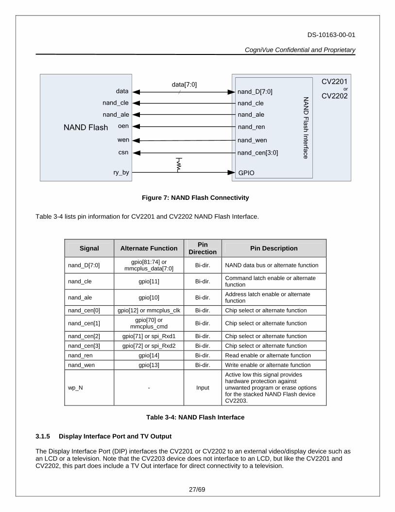
Figure 7 shows the connection between the CV2201 or CV2202 and a typical external NAND flash device. It should be noted that the ‘ry_by’ signal is not a dedicated pin on the CV2201 or CV2202. Instead this connection, required for command status, is made to a GPIO. Alternatively, a software managed polling routing may be used to determine when various commands are completed.
DS-10163-00-01 CogniVue Confidential and Proprietary
27/69
NAND Flash
CV2201or
CV2202nand_D[7:0]
nand_cle
nand_cen[3:0]
nand_ren
nand_wen
NA
ND
Flash Interface
data
csn
wen
oen
data[7:0]
nand_ale
nand_cle
nand_ale
ry_by GPIO
Figure 7: NAND Flash Connectivity
Table 3-4 lists pin information for CV2201 and CV2202 NAND Flash Interface.
Signal Alternate Function Pin Direction Pin Description
nand_D[7:0] gpio[81:74] or mmcplus_data[7:0] Bi-dir. NAND data bus or alternate function
nand_cle gpio[11] Bi-dir. Command latch enable or alternate function
nand_ale gpio[10] Bi-dir. Address latch enable or alternate function
nand_cen[0] gpio[12] or mmcplus_clk Bi-dir. Chip select or alternate function
nand_cen[1] gpio[70] or mmcplus_cmd Bi-dir. Chip select or alternate function
nand_cen[2] gpio[71] or spi_Rxd1 Bi-dir. Chip select or alternate function nand_cen[3] gpio[72] or spi_Rxd2 Bi-dir. Chip select or alternate function nand_ren gpio[14] Bi-dir. Read enable or alternate function nand_wen gpio[13] Bi-dir. Write enable or alternate function
wp_N - Input
Active low this signal provides hardware protection against unwanted program or erase options for the stacked NAND Flash device CV2203.
Table 3-4: NAND Flash Interface
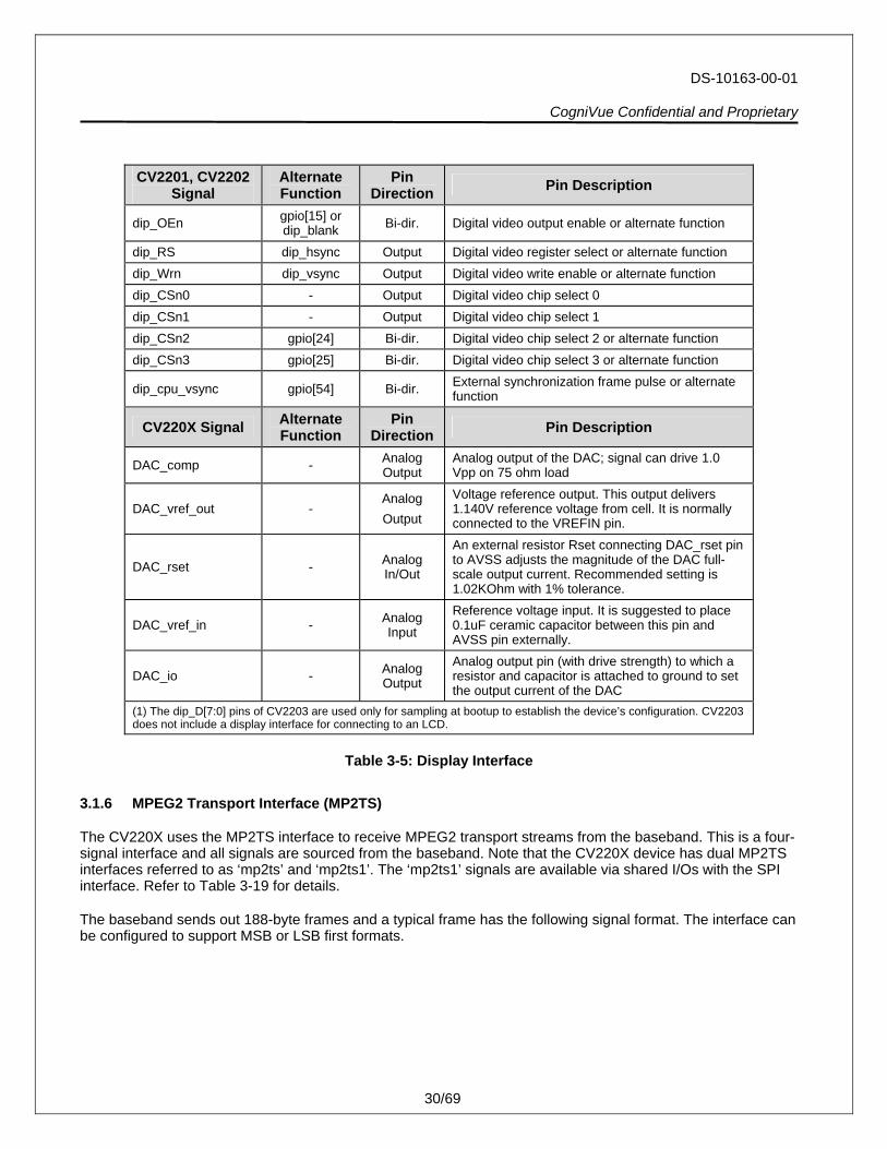
3.1.5 Display Interface Port and TV Output
The Display Interface Port (DIP) interfaces the CV2201 or CV2202 to an external video/display device such as an LCD or a television. Note that the CV2203 device does not interface to an LCD, but like the CV2201 and CV2202, this part does include a TV Out interface for direct connectivity to a television.
DS-10163-00-01 CogniVue Confidential and Proprietary
28/69
The external display controller in the CV2201 and CV2202 devices may be an RGB LCD and four CPU-like interface devices (MIPI/non-MIPI compliant).
The DIP has the following features:
• Picture-in-picture achieved through DMA descriptor fetching of appropriate image data
• Color format resizing (RGB24 -> RGB666/RGB565; RGB666->RGB24/RGB565; RGB565->RGB24/RGB666, YUV422->YUV444)
• Display Bus Interface (DBI): Drives an LCD, LCD Controller or CPU-type interface. Four chip selects are available to support up to four devices including any combination of LCD Controllers and/or other devices with CPU-type interfaces.
• Timing Interface: Drives an external video device (RBG LCD) with hsync/vsync/blank signals; when this mode is enabled, no CPU-LCD devices may be used. This interface supports up to XGA resolution.
• TV Interface: This analog interface derives timing information from an internal NTSC/PAL video encoder to drive video data at correct intervals. Maximum resolution supported is 640x480 (VGA).
Figure 8 shows a configuration with dual LCDs and a TV connection to the DIP. In this case, the internal CV220X video encoder and DAC are used to derive the analog TV signal.
LCD
data
cs
oe
we
rs
TV
LCD
CV220Xdip_Ddata
dip_CSn0csdip_CSn1
dip_OEn
dip_RS
oe
we dip_Wrn
DAC_io
rs
video_in
Second LCD
dip_CSn2dip_CSn3
DAC_AVDD
DAC_AVSS
DAC_vref_in
DAC_rset
DAC_vref_outDAC_comp
10uF
0.01uF
0.1uF
75 Ohm
1.02KOhm(+/- 1%)
3.3V
Figure 8: CPU-Type LCD and TV Connected to DIP (Using Internal DAC)
DS-10163-00-01 CogniVue Confidential and Proprietary
29/69
The figure below illustrates timing for DBI connectivity to a CPU-type interface.
Figure 9: DBI to CPU-type Display Waveform Diagram
Table 3-5 lists the CV2201 and CV2202 pin information for the DIP. The DAC signals correspond to the TV Output feature available for all CV220X products.
CV2201, CV2202 Signal
Alternate Function
Pin Direction Pin Description
dip_D[23] gpio[51] or uart1_txd Bi-dir. Digital video data or alternate function
dip_D[22] gpio[50] or uart1_rxd Bi-dir. Digital video data or alternate function
dip_D[21] gpio[49] Bi-dir. Digital video data or alternate function dip_D[20] gpio[48] Bi-dir. Digital video data or alternate function dip_D[19] gpio[47] Bi-dir. Digital video data or alternate function dip_D[18] gpio[46] Bi-dir. Digital video data or alternate function
dip_D[17] gpio[3] or scl_sec Bi-dir. Digital video data or alternate function
dip_D[16] gpio[4] or sda_sec Bi-dir. Digital video data or alternate function
dip_D[15:0] (1) - Bi-dir. Digital video data bus dip_pclk gpio[5] Bi-dir. Digital video pixel clock or alternate function
DS-10163-00-01 CogniVue Confidential and Proprietary
30/69
CV2201, CV2202 Signal
Alternate Function
Pin Direction Pin Description
dip_OEn gpio[15] or dip_blank Bi-dir. Digital video output enable or alternate function
dip_RS dip_hsync Output Digital video register select or alternate function dip_Wrn dip_vsync Output Digital video write enable or alternate function dip_CSn0 - Output Digital video chip select 0 dip_CSn1 - Output Digital video chip select 1 dip_CSn2 gpio[24] Bi-dir. Digital video chip select 2 or alternate function dip_CSn3 gpio[25] Bi-dir. Digital video chip select 3 or alternate function
dip_cpu_vsync gpio[54] Bi-dir. External synchronization frame pulse or alternate function
CV220X Signal Alternate Function
Pin Direction Pin Description
DAC_comp - Analog Output
Analog output of the DAC; signal can drive 1.0 Vpp on 75 ohm load
DAC_vref_out - Analog Output
Voltage reference output. This output delivers 1.140V reference voltage from cell. It is normally connected to the VREFIN pin.
DAC_rset - Analog In/Out
An external resistor Rset connecting DAC_rset pin to AVSS adjusts the magnitude of the DAC full-scale output current. Recommended setting is 1.02KOhm with 1% tolerance.
DAC_vref_in - Analog Input
Reference voltage input. It is suggested to place 0.1uF ceramic capacitor between this pin and AVSS pin externally.
DAC_io - Analog Output
Analog output pin (with drive strength) to which a resistor and capacitor is attached to ground to set the output current of the DAC
(1) The dip_D[7:0] pins of CV2203 are used only for sampling at bootup to establish the device’s configuration. CV2203 does not include a display interface for connecting to an LCD.
Table 3-5: Display Interface
3.1.6 MPEG2 Transport Interface (MP2TS)
The CV220X uses the MP2TS interface to receive MPEG2 transport streams from the baseband. This is a four-signal interface and all signals are sourced from the baseband. Note that the CV220X device has dual MP2TS interfaces referred to as ‘mp2ts’ and ‘mp2ts1’. The ‘mp2ts1’ signals are available via shared I/Os with the SPI interface. Refer to Table 3-19 for details.
The baseband sends out 188-byte frames and a typical frame has the following signal format. The interface can be configured to support MSB or LSB first formats.
DS-10163-00-01 CogniVue Confidential and Proprietary
31/69
Figure 10: MP2TS Interface Signal Formats
Table 3-6 lists the CV220X pin information for the MP2TS Interface.
Signal Alternate Function
Pin Direction Pin Description
mp2ts_clk - Input Clock source for synchronous interface
mp2ts_valid - Input Signal indicating the serial data is valid
mp2ts_sync - Input Frame pulse indicating start of frame
mp2ts_data - Input Serial data
Table 3-6: MP2TS Interface
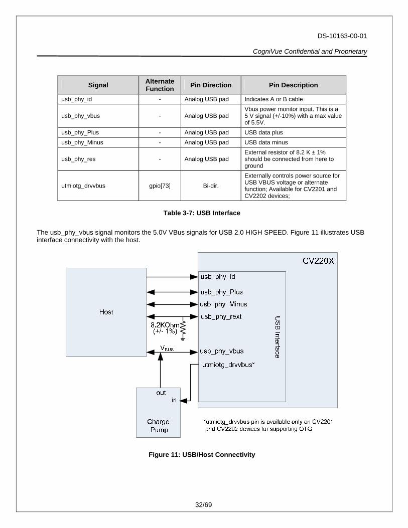
3.1.7 USB 2.0 HIGH SPEED
The USB Interface has the following features:
• USB 2.0 HIGH SPEED compliant
• CV2201 and CV2202 devices support USB OTG
• USB 2.0 PHY is integrated on chip
• Supports high-speed (480 MHz), full speed (12 MHz), and low speed (1.5 MHz) operation
• Supports seven physical endpoints - one control and six endpoints configurable as IN or OUT. The IN/OUT endpoints are software configurable as bulk, isochronous, interrupt or control
Table 3-7 lists the CV220X pin information for the USB Interface.
DS-10163-00-01 CogniVue Confidential and Proprietary
32/69
Signal Alternate Function Pin Direction Pin Description
usb_phy_id - Analog USB pad Indicates A or B cable
usb_phy_vbus - Analog USB pad Vbus power monitor input. This is a 5 V signal (+/-10%) with a max value of 5.5V.
usb_phy_Plus - Analog USB pad USB data plus usb_phy_Minus - Analog USB pad USB data minus
usb_phy_res - Analog USB pad External resistor of 8.2 K ± 1% should be connected from here to ground
utmiotg_drvvbus gpio[73] Bi-dir.
Externally controls power source for USB VBUS voltage or alternate function; Available for CV2201 and CV2202 devices;
Table 3-7: USB Interface
The usb_phy_vbus signal monitors the 5.0V VBus signals for USB 2.0 HIGH SPEED. Figure 11 illustrates USB interface connectivity with the host.
Figure 11: USB/Host Connectivity
DS-10163-00-01 CogniVue Confidential and Proprietary
33/69
3.1.8 Smart Card Interface
The Smart Card Interface complies with the following integrated circuit card standards:
• ISO/IEC 7816-3 amendment I (2002-06-01)
• ISO/IEC 7816-10
• EMV Book 1 Version 4.1 (2004-05-01)
The CV220X Smart Card feature supports:
• Programmable clock frequency, baud rate, activation time, de-activation time and others
• Hardware initiated de-activation sequence upon detection of card removal
• Charge pump control interface for smart card power supply control
Figure 12 shows the connection between the CV220X and a typical smart card device.
Figure 12: Smart Card Connectivity
Table 3-8 lists the CV220X pin information for the Smart Card Interface.
Signal Alternate Function
Pin Direction Pin Description
sc_io gpio[58] Bi-dir. Serial data I/O sc_card_detect gpio[59] Bi-dir. Card detection
sc_card_voltage gpio[61] or spi_rx3 Bi-dir. Output to external PS to indicate required
voltage or alternate function
DS-10163-00-01 CogniVue Confidential and Proprietary
34/69
Signal Alternate Function
Pin Direction Pin Description
sc_fcb gpio[57] or pwm1_out Bi-dir. Used in synchronous mode or alternate
function sc_clk gpio[55] Bi-dir. Clock or alternate function sc_power_on gpio[60] Bi-dir. Controls external PS or alternate function sc_rst gpio[56] Bi-dir. Reset or alternate function
Table 3-8: Smart Card Interface
3.1.9 Serial Interfaces
The CV220X has the following serial interfaces:
• UART
• SPI
3.1.9.1 UART
The CV220X has two UARTs, referred to as UART and UART1, used for incoming or outgoing data paths. Note that uart1_Rx and uart1_Tx signals of UART1 are available via shared I/Os and this UART does not support CTS/RTS modem signals.
The UARTs have the following features:
• Asynchronous interface
• Programmable baud rate
• Parity and framing error detection with indication via interrupts
• Echo, local loopback and remote loopback diagnostic modes
• Single start bit, 8-bit character length, programmable stop bits (1 or 2), programmable parity (even, odd or none)
• Independent receive and transmit FIFOs
• The primary UART supports CTS/RTS modem signals for hardware flow control.
Table 3-9 lists the CV220X pin information for the UART Interface.
DS-10163-00-01 CogniVue Confidential and Proprietary
35/69
Signal Alternate Function
Pin Direction Pin Description
uart_Rx gpio[23] Bi-dir. UART serial receive data or alternate function
uart_Tx gpio[22] Bi-dir. UART serial transmit data or alternate function
uart_cts gpio[82] or spi_CS1 Bi-dir. Clear to send modem signal or alternate function
uart_rts gpio[83] or spi_CS2 Bi-dir. Request to send modem signal or alternate function
Table 3-9: UART Interface
UART1 signals are accessible only as alternate functions. These signals are listed in Table 3-19: GPIOs and Alternate Functions Shared with External Pins.
3.1.9.2 SPI
The Serial Peripheral Interface (SPI) provides an alternate data path to and from the CV220X. The CV220X device has two SPI blocks on board referred to herein as SPI and SPI1. The SPI blocks in the CV2201 and CV2202 devices each have four chip selects (spi_CS, spi_CS1, spi_CS2, spi_CS3), four serial receive data signals (spi_Rx, spi_Rx1, spi_Rx2, spi_Rx3) and a serial transmit data signal (spi_Tx). (Note that three of the chip selects and three receive signals of SPI are accessible via shared I/Os). CV2203-A SPI has two chip selects (spi_CS, spi_CS3), two serial receive data signals (spi_Rx and spi_Rx3) and a serial transmit data signal (spi_Tx). (The spi_CS3 and spi_Rx3 are accessible as alternate functions for this device.) For more details, refer to Table 3-19.) SPI1 has a dedicated clock, a chip select, and transmit and receive I/Os as shown below in Table 3-10.
This interface is compatible with the Motorola SPI specification and provides the following features:
• Four wire synchronous full duplex interface using a clock, chip select, serialized receive data and serialized transmit data
• Configurable as master or slave. The master sources the clock and chip select and the slave sinks these pins.
• 128-byte transmit FIFO and 128-byte receive FIFO
• Programmable clock rate (master mode only)
• Programmable frame size
• Supports “continuous” mode of operation
• Programmable clock phase (SPH) and polarity (SPO)
Table 3-10 lists the CV220X pin information for the SPI.
DS-10163-00-01 CogniVue Confidential and Proprietary
36/69
Signal Alternate Function
Pin Type Pin Description
spi_Clk gpio[29] Bi-dir. SPI serial clock or alternate function spi_CS gpio[28] Bi-dir. SPI slave select or alternate function
spi_Tx gpio[26] Bi-dir. SPI serial transmit data or alternate function
spi_Rx gpio[27] Bi-dir. SPI serial receive data or alternate function
spi1_Clk mp2ts1_clk Bi-dir. SPI1 serial clock or alternate function spi1_CS mp2ts1_sync Bi-dir. SPI1 slave select or alternate function
spi1_Tx mp2ts1_valid Bi-dir. SPI1 serial transmit data or alternate function
spi1_Rx mp2ts1_data Bi-dir. SPI1 serial receive data or alternate function
Table 3-10: SPI Signals
3.1.10 GPS Inteface
The SPI block has an embedded alternate GPS function that stores data from a GPS source into the receive fifo. When this mode is enabled the SPI function can no longer use the receive FIFO (the transmit FIFO is still available for SPI transmit functions). The GPS interface is a very simple serial interface as shown below.
gps_clk
gps_s
gps_m0
gps_m1 (optional)
gps_m2 (optional)
Figure 13: GPS Interface
GPS interface signals are shared IOs of the mp2ts inteface and the uart interface. GPS interface signals are listed in the table below.
Signal Alternate Function
Pin Direction Pin Description
mp2ts_clk gps_clk Bi-dir. mp2ts clock or alternate function
mp2ts_valid gps_m0 Bi-dir. mp2ts valid serial data or alternate function
DS-10163-00-01 CogniVue Confidential and Proprietary
37/69
Signal Alternate Function
Pin Direction Pin Description
mp2ts_sync gps_m1 Bi-dir. mp2ts frame pulse or alternate function
mp2ts_data gps_s Bi-dir. mp2ts serial data or alternate function
uart_rts gps_m2 Bi-dir. request to send modem signal or alternate function
Table 3-11: GPS Interface
3.1.11 Audio Interface
The Audio Interface provides a direct connection to either voice quality or high-quality audio ADC/DAC. The Audio Interface has the following features:
• Supports I2S or AC97 interface protocol
• Supports full duplex data path
• Separate receive and transmit FIFOs
• Software configurable hardware interface to support a variety of I2S and AC97 applications
Figure 14 shows the CV2201/CV2202 audio interface connections to an audio DAC. The CV2203 device does not include an audio interface.
AudioDAC
CV2201/CV2202audio_clkr
audio_clkx
audio_dr
Audio Interface
clkr
dr
clkx
dx
audio_dx
audio_fsr
audio_fsx
fsr
fsx
mclkclk
Figure 14: Audio Interface
Table 3-12 lists the CV2201 and CV2202 pin information for the Audio Interface.
DS-10163-00-01 CogniVue Confidential and Proprietary
38/69
Signal Alternate Function
Pin Direction Pin Description
audio_clkr gpio[16] Bi-dir. Audio receive bit clock or alternate function audio_clkx gpio[19] Bi-dir. Audio transmit bit clock or alternate function audio_dr gpio[17] Bi-dir. Audio receive data or alternate function audio_dx gpio[20] Bi-dir. Audio transmit data or alternate function
audio_fsr gpio[18] or pwm2_out Bi-dir. Audio receive frame clock or alternate function
audio_fsx gpio[21] Bi-dir. Audio transmit frame clock or alternate function mclk - Bi-dir. Audio clock source from external audio DAC.
Table 3-12: Audio Interface
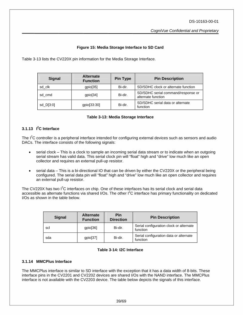
3.1.12 Media Storage (SD/SDHC)
The Media Storage Interface is compatible with the SD and SDHC memory card specifications. SDHC cards are supported but only at SD card interface rates. MMC is a subset of the SD specification and by default is also supported. The Media Storage Interface has the following features:
• Software programmable external clock
• Support of a 48-bit command through a software accessible command buffer
• Support of both a 48 or 136-bit response through a response buffer
• Support of CRC generation and checking
• Software configurable data width of 1 (MMC mode) or 4 bits (SD mode)
• Incoming and outgoing datapath (implemented using FIFOs) driven by a DMA engine
The interface does not manage the media card power supply. Figure 15 shows the connectivity between the CV220X and an SD memory card.
DS-10163-00-01 CogniVue Confidential and Proprietary
39/69
Figure 15: Media Storage Interface to SD Card
Table 3-13 lists the CV220X pin information for the Media Storage Interface.
Signal Alternate Function Pin Type Pin Description
sd_clk gpio[35] Bi-dir. SD/SDHC clock or alternate function
sd_cmd gpio[34] Bi-dir. SD/SDHC serial command/response or alternate function
sd_D[3:0] gpio[33:30] Bi-dir. SD/SDHC serial data or alternate function
Table 3-13: Media Storage Interface
3.1.13 I2C Interface
The I2C controller is a peripheral interface intended for configuring external devices such as sensors and audio DACs. The interface consists of the following signals:
• serial clock – This is a clock to sample an incoming serial data stream or to indicate when an outgoing serial stream has valid data. This serial clock pin will “float” high and “drive” low much like an open collector and requires an external pull-up resistor.
• serial data – This is a bi-directional IO that can be driven by either the CV220X or the peripheral being configured. The serial data pin will “float” high and “drive” low much like an open collector and requires an external pull-up resistor.
The CV220X has two I2C interfaces on chip. One of these interfaces has its serial clock and serial data accessible as alternate functions via shared I/Os. The other I2C interface has primary functionality on dedicated I/Os as shown in the table below.
Signal Alternate Function
Pin Direction Pin Description
scl gpio[36] Bi-dir. Serial configuration clock or alternate function
sda gpio[37] Bi-dir. Serial configuration data or alternate function
Table 3-14: I2C Interface
3.1.14 MMCPlus Interface
The MMCPlus interface is similar to SD interface with the exception that it has a data width of 8-bits. These interface pins in the CV2201 and CV2202 devices are shared I/Os with the NAND interface. The MMCPlus interface is not available with the CV2203 device. The table below depicts the signals of this interface.
DS-10163-00-01 CogniVue Confidential and Proprietary
40/69
Signal Alternate Function
Pin Direction Pin Description
nand_cen[0] gpio[12] or mmcplus_clk Bi-dir. NAND chip select0 or alternate
function
nand_cen[1] gpio[70] or mmcplus_cmd Bi-dir. NAND chip select1 or alternate
function
nand_D[0] gpio[74] or mmcplus_data[0] Bi-dir. NAND data bus signal or alternate
function
nand_D[1] gpio[75] or mmcplus_data[1] Bi-dir. NAND data bus signal or
alternate function
nand_D[2] gpio[76] or mmcplus_data[2] Bi-dir. NAND data bus signal or
alternate function
nand_D[3] gpio[77] or mmcplus_data[3] Bi-dir. NAND data bus signal or
alternate function
nand_D[4] gpio[78] or mmcplus_data[4] Bi-dir. NAND data bus signal or
alternate function
nand_D[5] gpio[79] or mmcplus_data[5] Bi-dir. NAND data bus signal or
alternate function
nand_D[6] gpio[80] or mmcplus_data[6] Bi-dir. NAND data bus signal or
alternate function
nand_D[7] gpio[81] or mmcplus_data[7] Bi-dir. NAND data bus signal or
alternate function
Table 3-15: MMCPlus Interface Pinout for CV2201, CV2202
3.1.15 External Memory Interface
The CV2202 device has a memory controller capable of interfacing with an external Mobile DDR SDRAM up to 1Gbit in size. Figure 16 illustrates the CV2202 connectivity to an external Mobile DDR SDRAM.
DS-10163-00-01 CogniVue Confidential and Proprietary
41/69
Mobile DDR SDRAM
CV2202
DQ[31:0]
A[12:0]
WEnRASnCASn
CKE
CSn
DM[3:0]
BA[1:0]
DMCLKDMCLKnclk_n
clk
clk_ena
cs_n
we_n
cas_nras_n
addr[12:0]bank_addr[1:0]
data_mask[3:0]
data_q[31:0]
data_strobe[3:0] DQS[3:0]
Figure 16: CV2202 Interface to External Memory
The table below provides CV2202 pin information for the memory interface.
Signal Alternate Function
Pin Direction Pin Description
DMCLK - Output Clock signal to external memory.
DMCLKn - Output DMCLK and DMCLKn are differential clocks to the external memory.
A[12:0] - Output Address bus
CKE - Output Clock enable signal for external memory
WEn - Output Write enable signal for external memory (active low)
CASn - Output Column access strobe (active low)
RASn - Output Row access strobe (active low)
CSn - Output Chip select (active low)
BA[1:0] - Output Bank address bus
DQ[31:0] - Bi-dir. Data bus
DS-10163-00-01 CogniVue Confidential and Proprietary
42/69
Signal Alternate Function
Pin Direction Pin Description
DM[3:0] - Output
Data mask for write data; DM[3] is mask bit for DQ[31:24] DM[2] is mask bit for DQ[23:16] DM[1] is mask bit for DQ[15:8] DM[0] is mask bit for DQ[7:0];
DQS[3:0] - Bi-dir.
Data strobe; DQS[3] is strobe bit for DQ[31:24] DQS[2] is strobe bit for DQ[23:16] DQS[1] is strobe bit for DQ[15:8] DQS[1] is strobe bit for DQ[7:0];
Table 3-16: CV2202 External Memory Pinout
3.1.16 Pulse Width Modulated Outputs
Two pulse width modulated (PWM) outputs are available as alternate pin functions. As shown in Table 3-17, these pins also have alternate GPIO functionality. To use the PWM functionality, the GPIO for the pin must be disabled and the PWM output must be enabled.
Signal Alternate Function
Pin Direction Pin Description
audio_fsr gpio[18] or pwm2 Bi-dir.
Audio receive frame clock, GPIO or PWM signal as alternate function; only applies to CV2201 and CV2202
sc_fcb gpio[57] or pwm1 Bi-dir. Smart card, GPIO or PWM signal as alternate function; applies to all CV220X parts
Table 3-17: PWM Function Pinout
3.1.17 Power Management Interface
The PMI controller is a peripheral interface intended to manage internal and external power sources (either to change the voltage level or disable the voltage completely). Note that dual master operation is not supported by this controller.
The PMI interface is a two wire interface consisting of the following signals:
• pmi_clk – The clock source of this controller. This is only driven during the active portion of a transaction, otherwise it is tri-stated.
• pmi_data – Bi-directional serial data. Data is always driven on the rising edge and sampled on the falling edge.
DS-10163-00-01 CogniVue Confidential and Proprietary
43/69
Signal Alternate Function
Pin Direction Pin Description
reserved_4 gpio[7] or pmi_data Bi-dir. GPIO or alternate function
reserved_3 gpio[6] or pmi_clk Bi-dir. GPIO or alternate function
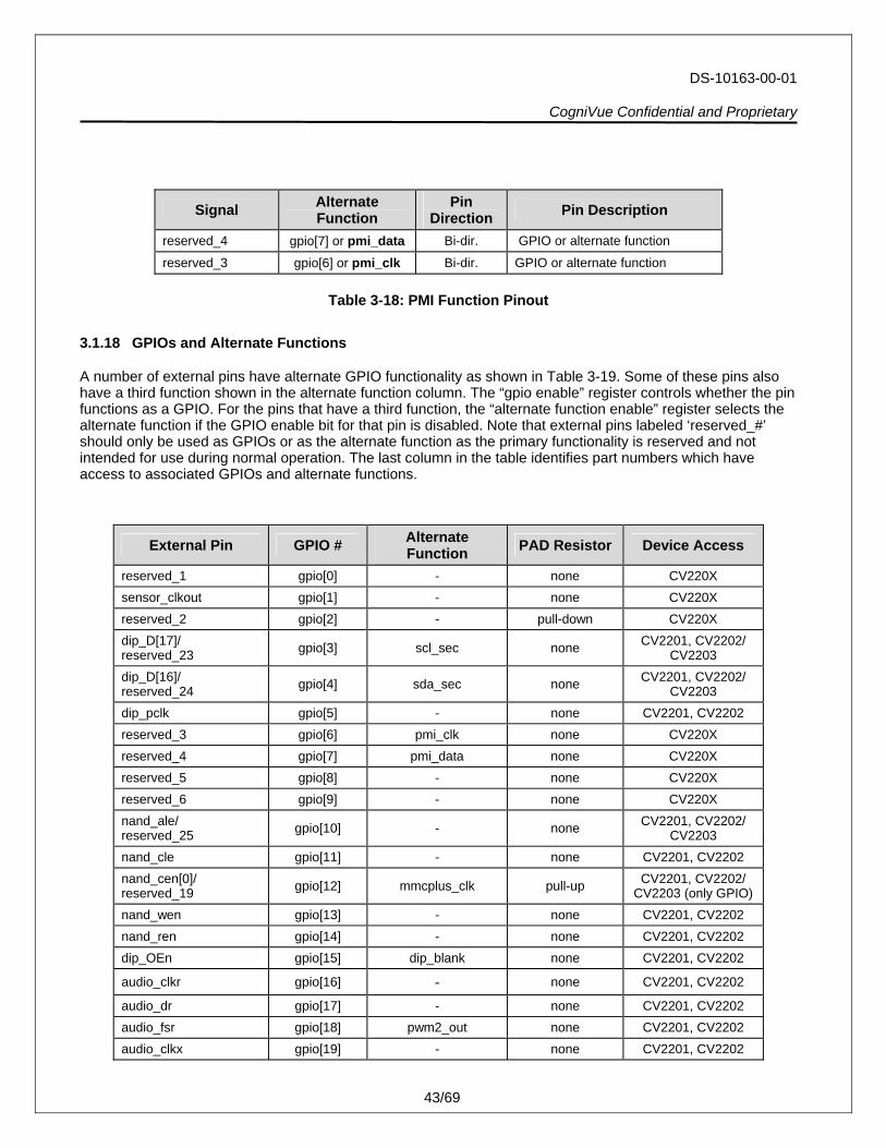
Table 3-18: PMI Function Pinout
3.1.18 GPIOs and Alternate Functions
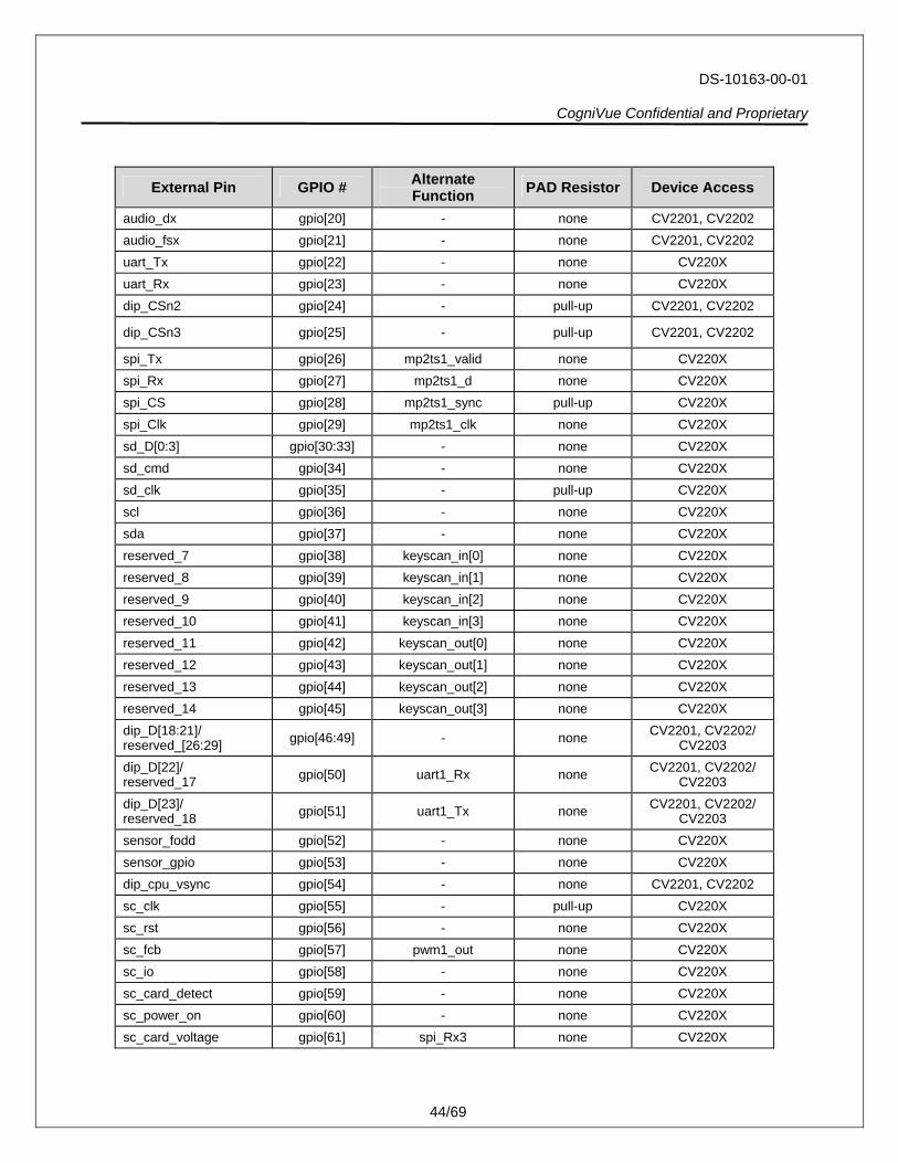
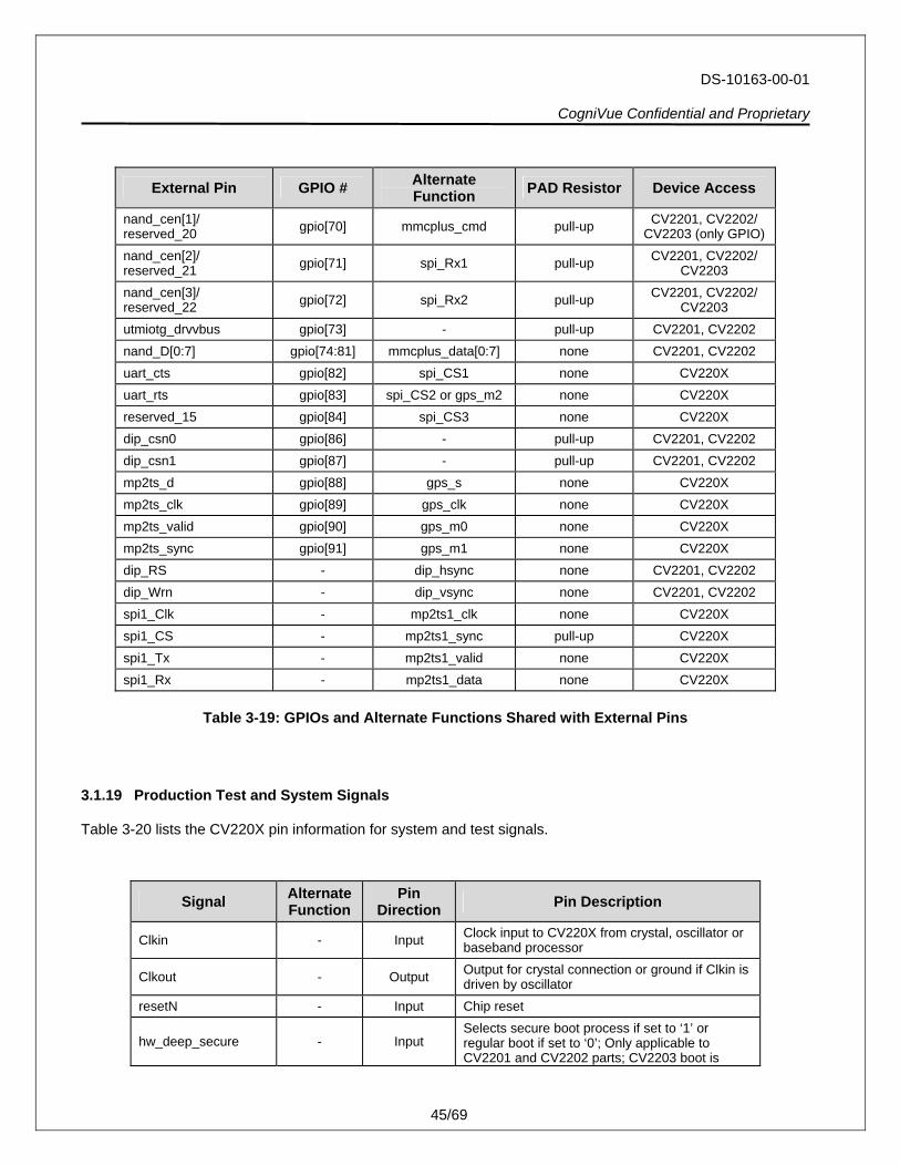
A number of external pins have alternate GPIO functionality as shown in Table 3-19. Some of these pins also have a third function shown in the alternate function column. The “gpio enable” register controls whether the pin functions as a GPIO. For the pins that have a third function, the “alternate function enable” register selects the alternate function if the GPIO enable bit for that pin is disabled. Note that external pins labeled ‘reserved_#’ should only be used as GPIOs or as the alternate function as the primary functionality is reserved and not intended for use during normal operation. The last column in the table identifies part numbers which have access to associated GPIOs and alternate functions.
External Pin GPIO # Alternate Function PAD Resistor Device Access
Table 3-19: GPIOs and Alternate Functions Shared with External Pins
3.1.19 Production Test and System Signals
Table 3-20 lists the CV220X pin information for system and test signals.
Signal Alternate Function
Pin Direction Pin Description
Clkin - Input Clock input to CV220X from crystal, oscillator or baseband processor
Clkout - Output Output for crystal connection or ground if Clkin is driven by oscillator
resetN - Input Chip reset
hw_deep_secure - Input Selects secure boot process if set to ‘1’ or regular boot if set to ‘0’; Only applicable to CV2201 and CV2202 parts; CV2203 boot is
DS-10163-00-01 CogniVue Confidential and Proprietary
46/69
Signal Alternate Function
Pin Direction Pin Description
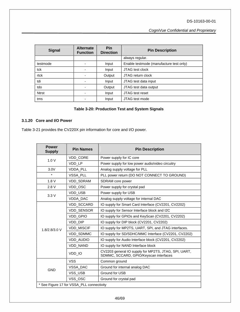
always regular. testmode - Input Enable testmode (manufacture test only) tck - Input JTAG test clock rtck - Output JTAG return clock tdi - Input JTAG test data input tdo - Output JTAG test data output Ntrst - Input JTAG test reset tms - Input JTAG test mode
Table 3-20: Production Test and System Signals
3.1.20 Core and I/O Power
Table 3-21 provides the CV220X pin information for core and I/O power.
Power Supply Pin Names Pin Description
VDD_CORE Power supply for IC core 1.0 V
VDD_LP Power supply for low power audio/video circuitry 3.0V VDDA_PLL Analog supply voltage for PLL
* VSSA_PLL PLL power return (DO NOT CONNECT TO GROUND) 1.8 V VDD_SDRAM SDRAM core power 2.8 V VDD_OSC Power supply for crystal pad
VDD_USB Power supply for USB 3.3 V
VDDA_DAC Analog supply voltage for internal DAC VDD_SCCARD IO supply for Smart Card Interface (CV2201, CV2202) VDD_SENSOR IO supply for Sensor Interface block and I2C VDD_GPIO IO supply for GPIOs and KeyScan (CV2201, CV2202) VDD_DIP IO supply for DIP block (CV2201, CV2202) VDD_MISCIF IO supply for MP2TS, UART, SPI, and JTAG interfaces. VDD_SDMMC IO supply for SD/SDHC/MMC Interface (CV2201, CV2202) VDD_AUDIO IO supply for Audio Interface block (CV2201, CV2202) VDD_NAND IO supply for NAND Interface block
1.8/2.8/3.0 V
VDD_IO CV2203 general IO supply for MP2TS, JTAG, SPI, UART, SDMMC, SCCARD, GPIO/Keyscan interfaces
VSS Common ground VSSA_DAC Ground for internal analog DAC VSS_USB Ground for USB
GND
VSS_OSC Ground for crystal pad * See Figure 17 for VSSA_PLL connectivity
DS-10163-00-01 CogniVue Confidential and Proprietary
47/69
Table 3-21: CV220X Power Supply
3.2 PLL and Timing Generation
The timing generation block provides and manages the clocks required by the internal logic and IP blocks. The clocks are produced from an internal PLL. An onboard crystal oscillator or an external clock provides the input clock to the PLL. Figure 17 shows the connection between crystals and the CV220X. If the clock source is the baseband processor or an oscillator, the clock output signals are not connected.
Figure 17: Crystal Connected to CV220X
DS-10163-00-01 CogniVue Confidential and Proprietary
48/69
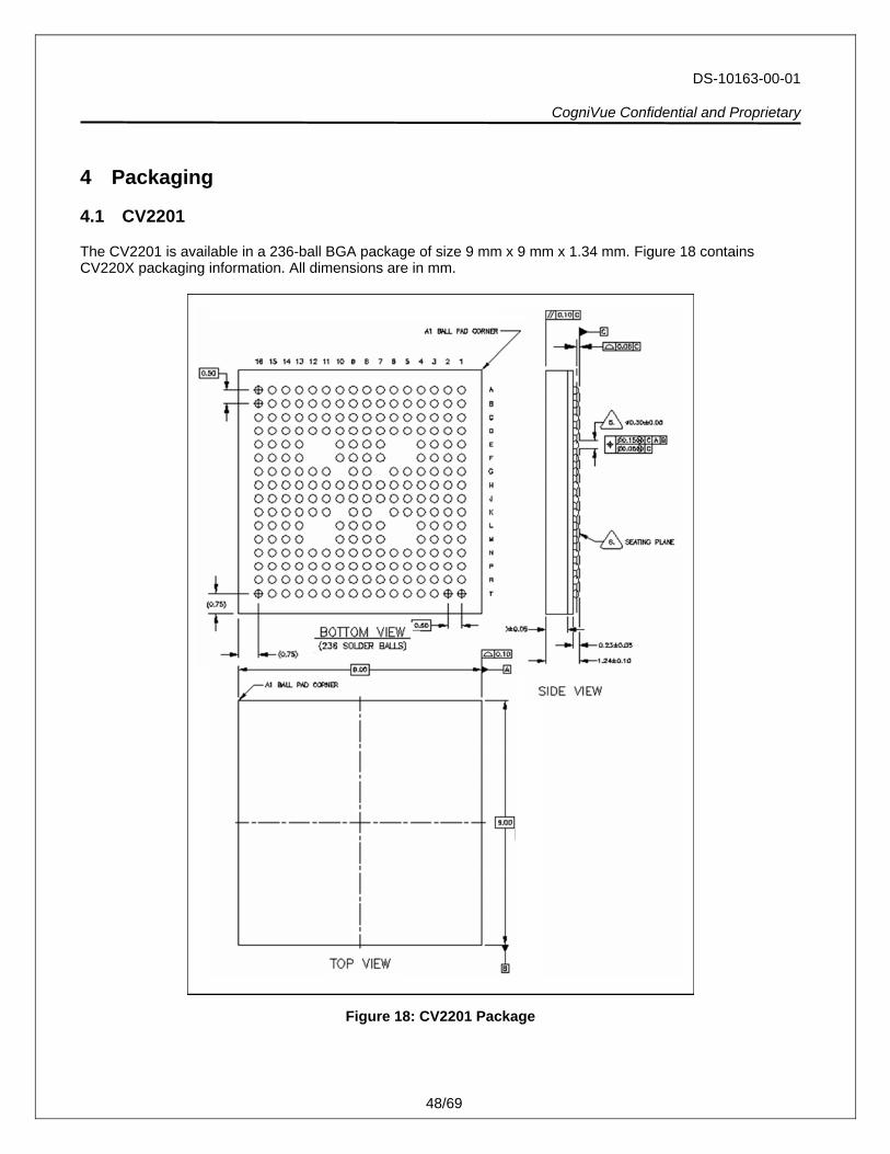
4 Packaging
4.1 CV2201
The CV2201 is available in a 236-ball BGA package of size 9 mm x 9 mm x 1.34 mm. Figure 18 contains CV220X packaging information. All dimensions are in mm.
Figure 18: CV2201 Package
DS-10163-00-01 CogniVue Confidential and Proprietary
49/69
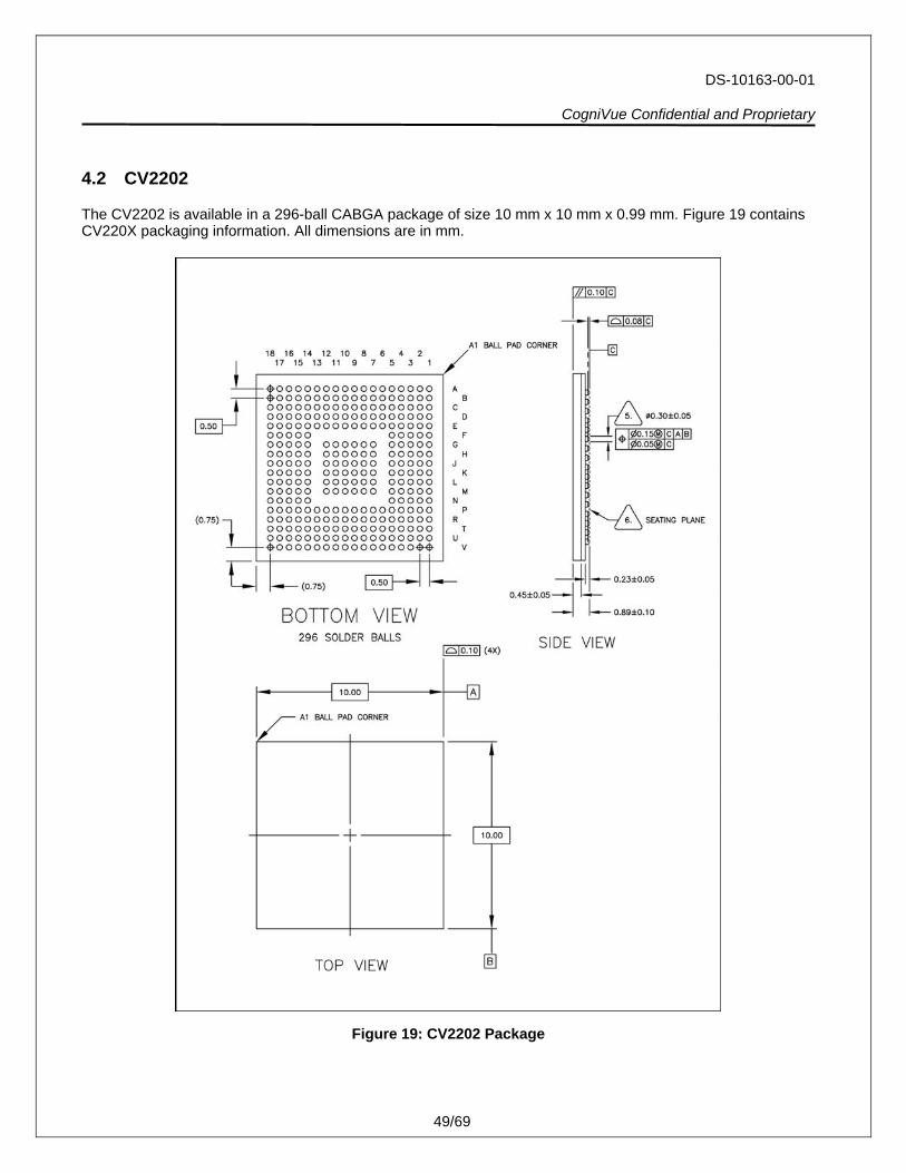
4.2 CV2202
The CV2202 is available in a 296-ball CABGA package of size 10 mm x 10 mm x 0.99 mm. Figure 19 contains CV220X packaging information. All dimensions are in mm.
Figure 19: CV2202 Package
DS-10163-00-01 CogniVue Confidential and Proprietary
50/69
4.3 CV2203
The CV2203 is available in a 196-ball BGA package of size 10 mm x 10 mm x 1.44 mm. Figure 20 contains CV220X packaging information. All dimensions are in mm.
Figure 20: CV2203 Package
DS-10163-00-01 CogniVue Confidential and Proprietary
51/69
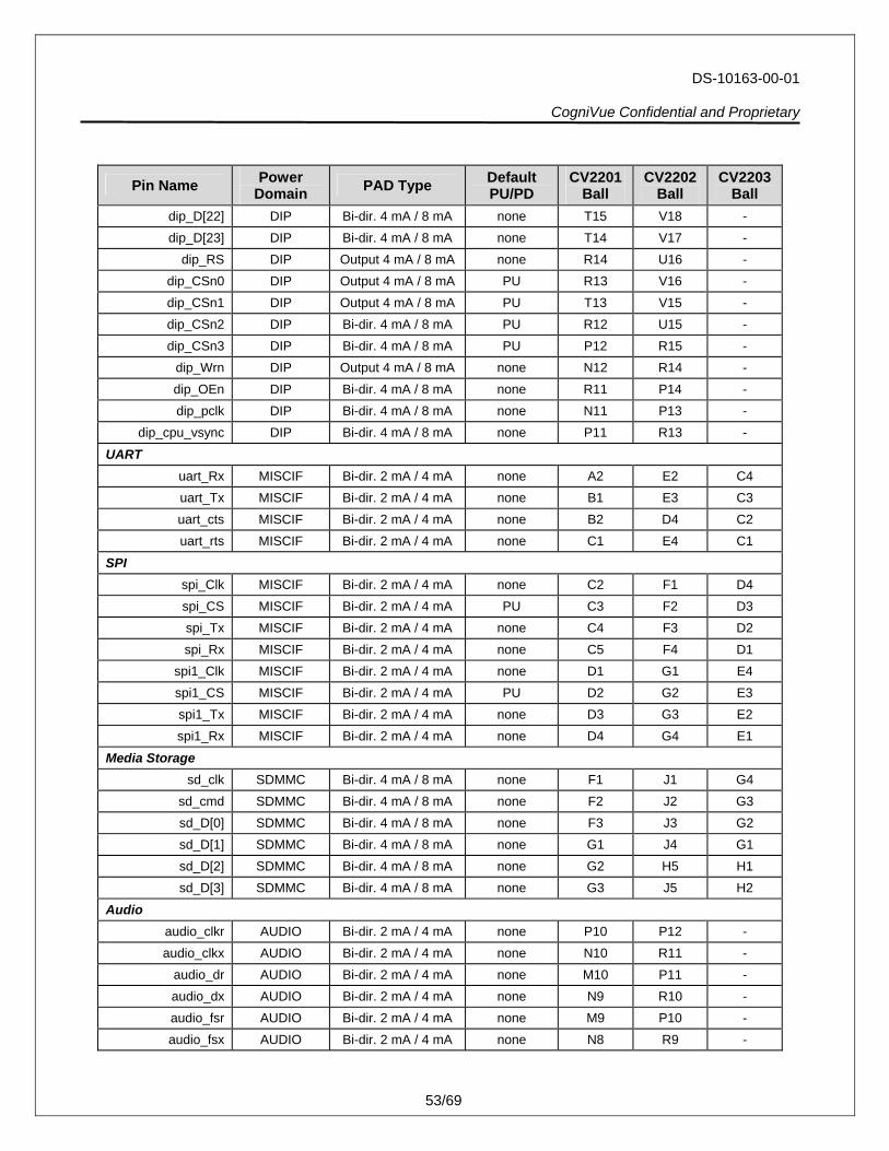
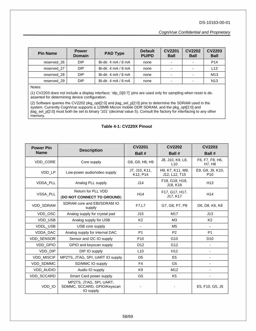
4.4 CV220X Pinout
The following table describes the physical pins of the devices belonging to the CV220X series. The pins are organized into functional groups. External interfaces are grouped together on the IO voltage banks that can be powered by either 2.8 or 1.8 volts. Many outputs may be configured as having low or high output drive strength by programming the device. The output drive capability is indicated in the PAD type column.
Note that ‘-’ indicates the pin does not apply to the device as the signal is not balled out on the package. Pins in the ‘No Connect’ section of the table are used solely for test purposes and should not be used in normal operating mode. Some pins are designated ‘reserved_#’. These pins may only be used as the corresponding GPIOs or alternate functionality as defined in section 3.1.18. Primary functionality of these pins is reserved and not intended for use.
sensor_fodd SIF Bi-dir. 4 mA / 8 mA none C10 E12 B9 sensor_gpio SIF Bi-dir. 4 mA / 8 mA none B7 D6 B4
sensor_clkout SIF Bi-dir. 4 mA / 8 mA none B10 D12 A9
I2C scl SIF Bi-dir. 4 mA / 8 mA none E10 D14 B10
sda SIF Bi-dir. 4 mA / 8 mA none D10 D13 C9
NAND nand_wen NAND Bi-dir. 2 mA / 4 mA none R1 V1 - nand_ren NAND Bi-dir. 2 mA / 4 mA none T1 V2 -
nand_cen[3] NAND Bi-dir. 2 mA / 4 mA PU K3 U3 - nand_cen[2] NAND Bi-dir. 2 mA / 4 mA PU T2 T3 - nand_cen[1] NAND Bi-dir. 2 mA / 4 mA PU R2 R3 - nand_cen[0] NAND Bi-dir. 2 mA / 4 mA PU P2 P3 -
nand_ale NAND Bi-dir. 2 mA / 4 mA none L3 V3 -
DS-10163-00-01 CogniVue Confidential and Proprietary
52/69
Pin Name Power Domain PAD Type Default
PU/PD CV2201
Ball CV2202
Ball CV2203
Ball nand_cle NAND Bi-dir. 2 mA / 4 mA none M3 P4 -
nand_D[0] NAND Bi-dir. 2 mA / 4 mA none N3 R4 - nand_D[1] NAND Bi-dir. 2 mA / 4 mA none P3 T4 - nand_D[2] NAND Bi-dir. 2 mA / 4 mA none K4 U4 - nand_D[3] NAND Bi-dir. 2 mA / 4 mA none N4 V4 - nand_D[4] NAND Bi-dir. 2 mA / 4 mA none P4 R5 - nand_D[5] NAND Bi-dir. 2 mA / 4 mA none K5 T5 - nand_D[6] NAND Bi-dir. 2 mA / 4 mA none N5 U5 - nand_D[7] NAND Bi-dir. 2 mA / 4 mA none N6 V5 -
wp_N NAND Input none - - K5
DAC DAC_comp DAC Analog I/O none L2 T1 N2
DAC_vref_out DAC Analog I/O none M1 T2 P2 DAC_rset DAC Analog I/O none M2 U2 N3
DAC_vref_in DAC Analog I/O none N2 U1 P3 DAC_io DAC Analog I/O none L1 R1 N1
Display Interface Port dip_D[0] DIP Bi-dir. 4 mA / 8 mA PD K16 L16 M8 (1) dip_D[1] DIP Bi-dir. 4 mA / 8 mA PU K15 L15 N8 (1) dip_D[2] DIP Bi-dir. 4 mA / 8 mA PD K14 L14 P8 (1) dip_D[3] DIP Bi-dir. 4 mA / 8 mA PD K13 M16 M9 (1) dip_D[4] DIP Bi-dir. 4 mA / 8 mA PU J13 M15 N9 (1) dip_D[5] DIP Bi-dir. 4 mA / 8 mA PD L16 M14 P9 (1) dip_D[6] DIP Bi-dir. 4 mA / 8 mA PD L15 N18 L10 (1) dip_D[7] DIP Bi-dir. 4 mA / 8 mA PD L14 N17 M10 (1) dip_D[8] DIP Bi-dir. 4 mA / 8 mA PD L13 N16 - dip_D[9] DIP Bi-dir. 4 mA / 8 mA none M16 N15 - dip_D10] DIP Bi-dir. 4 mA / 8 mA none M15 N14 -
dip_D[11] DIP Bi-dir. 4 mA / 8 mA none M14 P18 - dip_D[12] DIP Bi-dir. 4 mA / 8 mA none M13 P17 - dip_D[13] DIP Bi-dir. 4 mA / 8 mA none N16 P16 - dip_D[14] DIP Bi-dir. 4 mA / 8 mA none N15 P15 - dip_D[15] DIP Bi-dir. 4 mA / 8 mA none N14 R18 - dip_D[16] DIP Bi-dir. 4 mA / 8 mA none N13 R17 - dip_D[17] DIP Bi-dir. 4 mA / 8 mA none P16 R16 - dip_D[18] DIP Bi-dir. 4 mA / 8 mA none P15 T18 - dip_D[19] DIP Bi-dir. 4 mA / 8 mA none R16 T17 - dip_D[20] DIP Bi-dir. 4 mA / 8 mA none R15 U18 - dip_D[21] DIP Bi-dir. 4 mA / 8 mA none T16 U17 -
DS-10163-00-01 CogniVue Confidential and Proprietary
53/69
Pin Name Power Domain PAD Type Default
PU/PD CV2201
Ball CV2202
Ball CV2203
Ball dip_D[22] DIP Bi-dir. 4 mA / 8 mA none T15 V18 - dip_D[23] DIP Bi-dir. 4 mA / 8 mA none T14 V17 -
dip_RS DIP Output 4 mA / 8 mA none R14 U16 - dip_CSn0 DIP Output 4 mA / 8 mA PU R13 V16 - dip_CSn1 DIP Output 4 mA / 8 mA PU T13 V15 - dip_CSn2 DIP Bi-dir. 4 mA / 8 mA PU R12 U15 - dip_CSn3 DIP Bi-dir. 4 mA / 8 mA PU P12 R15 -
dip_Wrn DIP Output 4 mA / 8 mA none N12 R14 - dip_OEn DIP Bi-dir. 4 mA / 8 mA none R11 P14 - dip_pclk DIP Bi-dir. 4 mA / 8 mA none N11 P13 -
dip_cpu_vsync DIP Bi-dir. 4 mA / 8 mA none P11 R13 -
UART uart_Rx MISCIF Bi-dir. 2 mA / 4 mA none A2 E2 C4 uart_Tx MISCIF Bi-dir. 2 mA / 4 mA none B1 E3 C3 uart_cts MISCIF Bi-dir. 2 mA / 4 mA none B2 D4 C2 uart_rts MISCIF Bi-dir. 2 mA / 4 mA none C1 E4 C1
SPI spi_Clk MISCIF Bi-dir. 2 mA / 4 mA none C2 F1 D4 spi_CS MISCIF Bi-dir. 2 mA / 4 mA PU C3 F2 D3 spi_Tx MISCIF Bi-dir. 2 mA / 4 mA none C4 F3 D2 spi_Rx MISCIF Bi-dir. 2 mA / 4 mA none C5 F4 D1
spi1_Clk MISCIF Bi-dir. 2 mA / 4 mA none D1 G1 E4 spi1_CS MISCIF Bi-dir. 2 mA / 4 mA PU D2 G2 E3 spi1_Tx MISCIF Bi-dir. 2 mA / 4 mA none D3 G3 E2 spi1_Rx MISCIF Bi-dir. 2 mA / 4 mA none D4 G4 E1
Media Storage sd_clk SDMMC Bi-dir. 4 mA / 8 mA none F1 J1 G4
sd_cmd SDMMC Bi-dir. 4 mA / 8 mA none F2 J2 G3 sd_D[0] SDMMC Bi-dir. 4 mA / 8 mA none F3 J3 G2 sd_D[1] SDMMC Bi-dir. 4 mA / 8 mA none G1 J4 G1 sd_D[2] SDMMC Bi-dir. 4 mA / 8 mA none G2 H5 H1 sd_D[3] SDMMC Bi-dir. 4 mA / 8 mA none G3 J5 H2
Audio audio_clkr AUDIO Bi-dir. 2 mA / 4 mA none P10 P12 - audio_clkx AUDIO Bi-dir. 2 mA / 4 mA none N10 R11 -
audio_dr AUDIO Bi-dir. 2 mA / 4 mA none M10 P11 - audio_dx AUDIO Bi-dir. 2 mA / 4 mA none N9 R10 - audio_fsr AUDIO Bi-dir. 2 mA / 4 mA none M9 P10 - audio_fsx AUDIO Bi-dir. 2 mA / 4 mA none N8 R9 -
DS-10163-00-01 CogniVue Confidential and Proprietary
DS-10163-00-01 CogniVue Confidential and Proprietary
57/69
Pin Name Power Domain PAD Type Default
PU/PD CV2201
Ball CV2202
Ball CV2203
Ball D16, D15, D14, D13, E16, E15,
E14
Reserved Pins reserved_1 HPI Bi-dir. 2 mA / 4 mA none C14 D16 B14 reserved_2 HPI Bi-dir. 2 mA / 4 mA PD C15 D17 B13 reserved_3 HPI Bi-dir. 2 mA / 4 mA none G11 J14 H11 reserved_4 HPI Bi-dir. 2 mA / 4 mA none H13 K16 G12 reserved_5 HPI Bi-dir. 2 mA / 4 mA none G12 J15 G13 reserved_6 HPI Bi-dir. 2 mA / 4 mA none H12 K15 G14 reserved_7 HPI Bi-dir. 4 mA / 8 mA none G14 H14 F14 reserved_8 HPI Bi-dir. 4 mA / 8 mA none G15 H15 F13 reserved_9 HPI Bi-dir. 4 mA / 8 mA none G16 H16 F12
reserved_10 HPI Bi-dir. 4 mA / 8 mA none F13 G14 F11 reserved_11 HPI Bi-dir. 4 mA / 8 mA none F14 G15 E14 reserved_12 HPI Bi-dir. 4 mA / 8 mA none F15 G16 E13 reserved_13 HPI Bi-dir. 4 mA / 8 mA none F16 F14 E12 reserved_14 HPI Bi-dir. 4 mA / 8 mA none E13 F15 E11 reserved_15 HPI Bi-dir. 2 mA / 4 mA none G13 J16 G11 reserved_16 NAND Input none - - K12 reserved_17 DIP Bi-dir. 4 mA / 8 mA none - - P13 reserved_18 DIP Bi-dir. 4 mA / 8 mA none - - P12 reserved_19 NAND Bi-dir. 2 mA / 4 mA PU - - N4 reserved_20 NAND Bi-dir. 2 mA / 4 mA PU - - P4 reserved_21 NAND Bi-dir. 2 mA / 4 mA PU - - N5 reserved_22 NAND Bi-dir. 2 mA / 4 mA PU - - P5 reserved_23 DIP Bi-dir. 4 mA / 8 mA none - - N14 reserved_24 DIP Bi-dir. 4 mA / 8 mA none - - M14 reserved_25 NAND Bi-dir. 2 mA / 4 mA none - - P6
DS-10163-00-01 CogniVue Confidential and Proprietary
58/69
Pin Name Power Domain PAD Type Default
PU/PD CV2201
Ball CV2202
Ball CV2203
Ball reserved_26 DIP Bi-dir. 4 mA / 8 mA none - - P14 reserved_27 DIP Bi-dir. 4 mA / 8 mA none - - L13 reserved_28 DIP Bi-dir. 4 mA / 8 mA none - - M13 reserved_29 DIP Bi-dir. 4 mA / 8 mA none - - N13
Notes: (1) CV2203 does not include a display interface; ‘dip_D[0:7]’ pins are used only for sampling when reset is de-asserted for determining device configuration. (2) Software queries the CV2202 pkg_opt[2:0] and jtag_sel_p[2:0] pins to determine the SDRAM used in the system. Currently CogniVue supports a 128MB Micron mobile DDR SDRAM, and the pkg_opt[2:0] and jtag_sel_p[2:0] must both be set to binary ‘101’ (decimal value 5). Consult the factory for interfacing to any other memory.
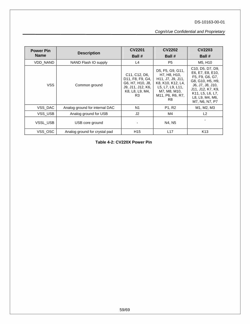
VSS_DAC Analog ground for internal DAC N1 P1, R2 M1, M2, M3 VSS_USB Analog ground for USB J2 M4 L2
VSSL_USB USB core ground - N4, N5 -
VSS_OSC Analog ground for crystal pad H15 L17 K13
Table 4-2: CV220X Power Pin
DS-10163-00-01 CogniVue Confidential and Proprietary
60/69
5 Electrical Specifications
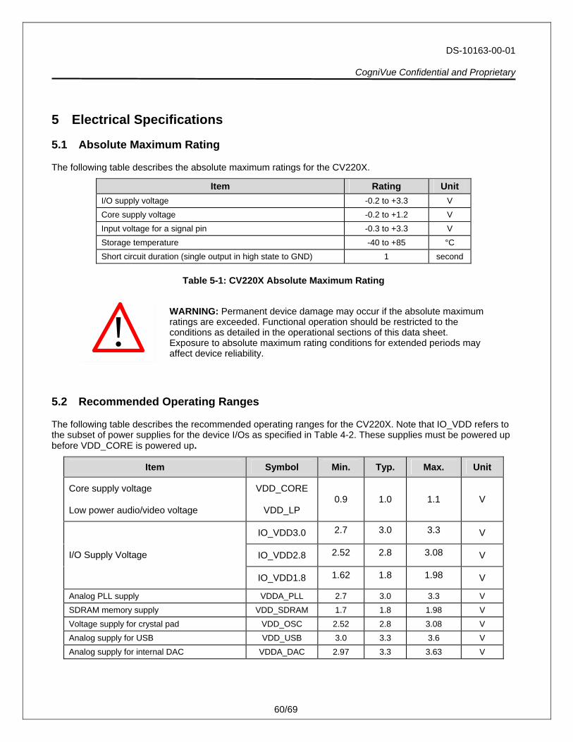
5.1 Absolute Maximum Rating
The following table describes the absolute maximum ratings for the CV220X.
Item Rating Unit I/O supply voltage -0.2 to +3.3 V Core supply voltage -0.2 to +1.2 V Input voltage for a signal pin -0.3 to +3.3 V Storage temperature -40 to +85 °C Short circuit duration (single output in high state to GND) 1 second
Table 5-1: CV220X Absolute Maximum Rating
!
WARNING: Permanent device damage may occur if the absolute maximum ratings are exceeded. Functional operation should be restricted to the conditions as detailed in the operational sections of this data sheet. Exposure to absolute maximum rating conditions for extended periods may affect device reliability.
5.2 Recommended Operating Ranges
The following table describes the recommended operating ranges for the CV220X. Note that IO_VDD refers to the subset of power supplies for the device I/Os as specified in Table 4-2. These supplies must be powered up before VDD_CORE is powered up.
Item Symbol Min. Typ. Max. Unit
Core supply voltage
Low power audio/video voltage
VDD_CORE
VDD_LP 0.9 1.0 1.1 V
IO_VDD3.0 2.7 3.0 3.3 V
IO_VDD2.8 2.52 2.8 3.08 V I/O Supply Voltage
IO_VDD1.8 1.62 1.8 1.98 V
Analog PLL supply VDDA_PLL 2.7 3.0 3.3 V SDRAM memory supply VDD_SDRAM 1.7 1.8 1.98 V Voltage supply for crystal pad VDD_OSC 2.52 2.8 3.08 V Analog supply for USB VDD_USB 3.0 3.3 3.6 V Analog supply for internal DAC VDDA_DAC 2.97 3.3 3.63 V
DS-10163-00-01 CogniVue Confidential and Proprietary
61/69
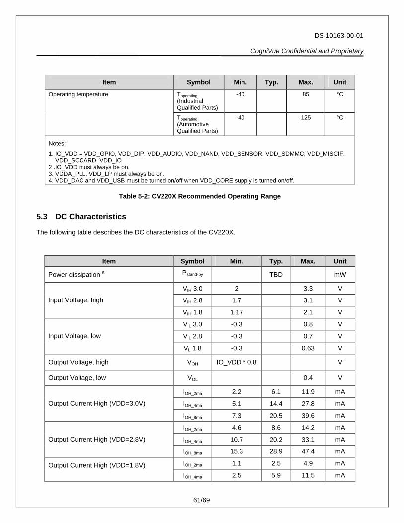
Item Symbol Min. Typ. Max. Unit
Toperating (Industrial Qualified Parts)
-40 85 °C Operating temperature
Toperating (Automotive Qualified Parts)
-40 125 °C
Notes:
1. IO_VDD = VDD_GPIO, VDD_DIP, VDD_AUDIO, VDD_NAND, VDD_SENSOR, VDD_SDMMC, VDD_MISCIF, VDD_SCCARD, VDD_IO 2 .IO_VDD must always be on. 3. VDDA_PLL, VDD_LP must always be on. 4. VDD_DAC and VDD_USB must be turned on/off when VDD_CORE supply is turned on/off.
Table 5-2: CV220X Recommended Operating Range
5.3 DC Characteristics
The following table describes the DC characteristics of the CV220X.
Item Symbol Min. Typ. Max. Unit
Power dissipation a Pstand-by TBD mW
VIH 3.0 2 3.3 V
VIH 2.8 1.7 3.1 V Input Voltage, high
VIH 1.8 1.17 2.1 V
VIL 3.0 -0.3 0.8 V
VIL 2.8 -0.3 0.7 V Input Voltage, low
VL 1.8 -0.3 0.63 V
Output Voltage, high VOH IO_VDD * 0.8 V
Output Voltage, low VOL 0.4 V
IOH_2ma 2.2 6.1 11.9 mA
IOH_4ma 5.1 14.4 27.8 mA Output Current High (VDD=3.0V)
IOH_8ma 7.3 20.5 39.6 mA
IOH_2ma 4.6 8.6 14.2 mA
IOH_4ma 10.7 20.2 33.1 mA Output Current High (VDD=2.8V)
IOH_8ma 15.3 28.9 47.4 mA
IOH_2ma 1.1 2.5 4.9 mA Output Current High (VDD=1.8V) IOH_4ma 2.5 5.9 11.5 mA
DS-10163-00-01 CogniVue Confidential and Proprietary
62/69
Item Symbol Min. Typ. Max. Unit IOH_8ma 3.6 8.5 16.5 mA
IOL_2ma 2.8 5 7.8 mA
IOL_4ma 5.6 9.5 15.5 mA Output Current Low (VDD=3.0V)
IOL_8ma 8.4 15 23.5 mA
IOL_2ma 3.9 7 11 mA
IOL_4ma 7.8 13.9 21.9 mA Output Current Low (VDD=2.8V)
IOL_8ma 11.8 21.1 33.2 mA
IOL_2ma 1.4 2.8 4.8 mA
IOL_4ma 2.9 5.6 9.6 mA Output Current Low (VDD=1.8V)
IOL_8ma 4.4 8.4 14.5 mA
Input Capacitance CI 4 pF
a. Active standby power measurements are determined based on the following: code is loaded and running, processor and memory are active (ie. memory is not in self-refresh mode), ARM is in low power idle mode waiting for an event to wake it up and process something, and VDD_CORE is off.
Table 5-3: CV220X DC Characteristics
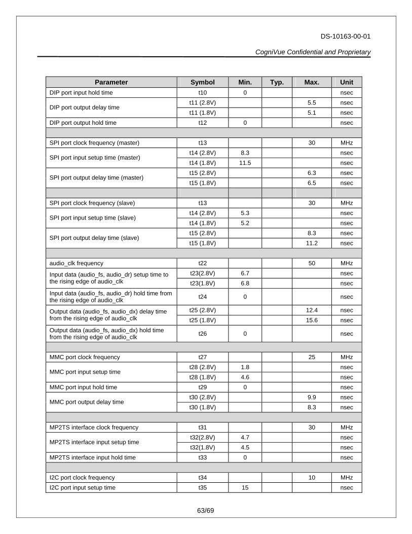
5.4 AC Specifications
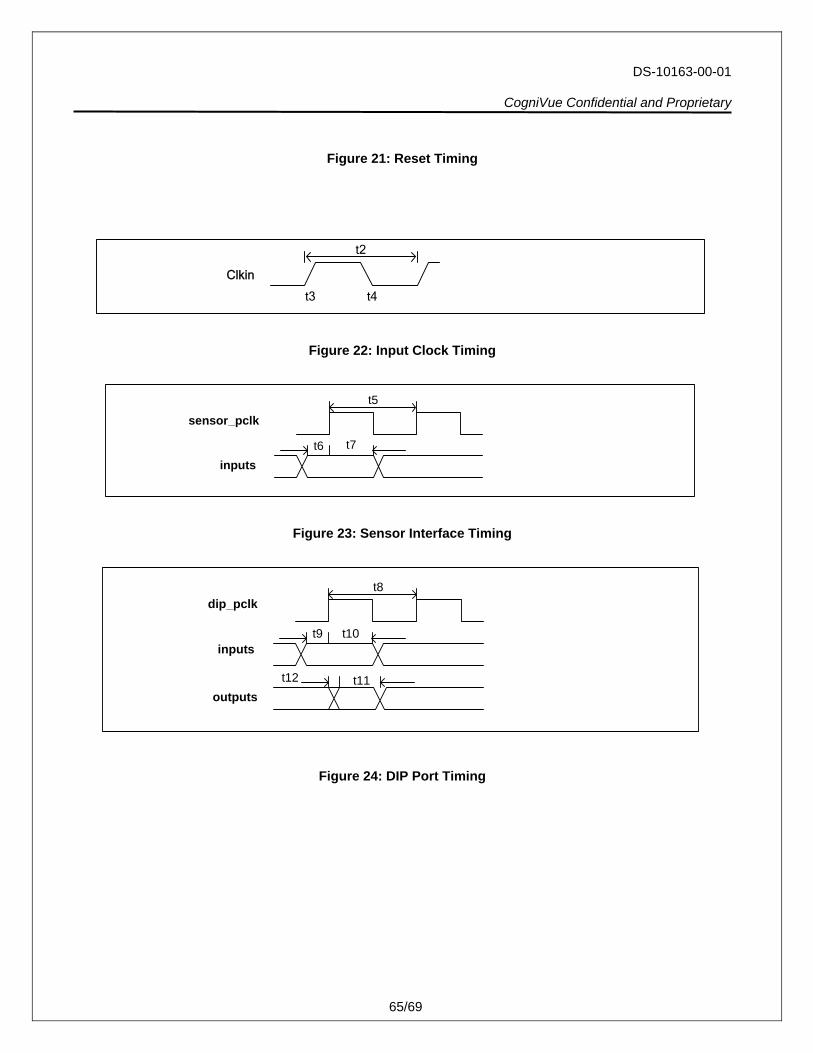
The following table provides the CV220X external interface timing. Figure 21 to Figure 32 illustrate specific waveforms for each interface.
Parameter Symbol Min. Typ. Max. Unit Reset pulse width t1 1 usec
Input clock period t2 10 30 MHz Input clock rise time t3 4 nsec Input clock fall time t4 4 nsec Input clock duty cycle 40 50 60 %
Sensor pixel clock period t5 6.25 nsec
t6(2.8V) 4.35 nsec Sensor input setup time
t6(1.8V) 4.15 nsec Sensor input hold time t7 0 nsec
DIP port pixel clock frequency t8 70 MHz
t9 (2.8V) 7.4 nsec DIP port input setup time
t9 (1.8V) 9.2 nsec
DS-10163-00-01 CogniVue Confidential and Proprietary
63/69
Parameter Symbol Min. Typ. Max. Unit DIP port input hold time t10 0 nsec
t11 (2.8V) 5.5 nsec DIP port output delay time
t11 (1.8V) 5.1 nsec DIP port output hold time t12 0 nsec
SPI port clock frequency (master) t13 30 MHz
t14 (2.8V) 8.3 nsec SPI port input setup time (master)
t14 (1.8V) 11.5 nsec t15 (2.8V) 6.3 nsec
SPI port output delay time (master) t15 (1.8V) 6.5 nsec
SPI port clock frequency (slave) t13 30 MHz
t14 (2.8V) 5.3 nsec SPI port input setup time (slave)
t14 (1.8V) 5.2 nsec t15 (2.8V) 8.3 nsec
SPI port output delay time (slave) t15 (1.8V) 11.2 nsec
audio_clk frequency t22 50 MHz
t23(2.8V) 6.7 nsec Input data (audio_fs, audio_dr) setup time to the rising edge of audio_clk t23(1.8V) 6.8 nsec Input data (audio_fs, audio_dr) hold time from the rising edge of audio_clk t24 0 nsec
t25 (2.8V) 12.4 nsec Output data (audio_fs, audio_dx) delay time from the rising edge of audio_clk t25 (1.8V) 15.6 nsec Output data (audio_fs, audio_dx) hold time from the rising edge of audio_clk t26 0 nsec
MMC port clock frequency t27 25 MHz
t28 (2.8V) 1.8 nsec MMC port input setup time
t28 (1.8V) 4.6 nsec MMC port input hold time t29 0 nsec
t30 (2.8V) 9.9 nsec MMC port output delay time
t30 (1.8V) 8.3 nsec
MP2TS interface clock frequency t31 30 MHz t32(2.8V) 4.7 nsec
MP2TS interface input setup time t32(1.8V) 4.5 nsec
MP2TS interface input hold time t33 0 nsec
I2C port clock frequency t34 10 MHz I2C port input setup time t35 15 nsec
DS-10163-00-01 CogniVue Confidential and Proprietary
64/69
Parameter Symbol Min. Typ. Max. Unit I2C port input hold time t36 0 nsec I2C port output delay time t37 15 nsec I2C port output hold time t38 0 nsec
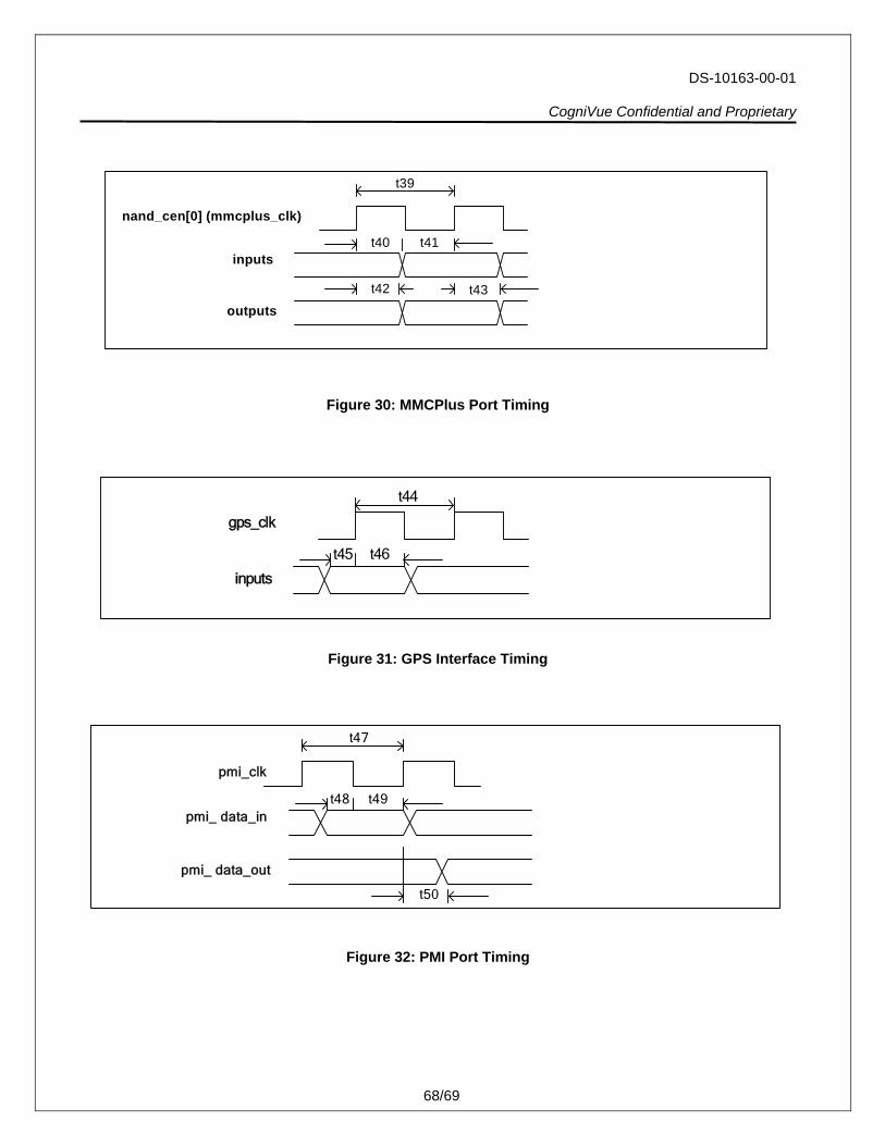
MMCplus port clock frequency t39 52 MHz
MMCplus port input hold time t40 5 nsec
t41 (2.8V) 3.5 nsec MMCplus port input setup time
t41 (1.8V) 6.6 nsec
MMCplus port output hold time t42 3 nsec
t43 (2.8V) 16.5 nsec MMCplus port output delay time
t43 (1.8V) 16.7 nsec
GPS clock period t44 20 MHz
t45(2.8V) 5.1 nsec GPS setup time
t45(1.8V) 5 nsec
GPS hold time t46 0 nsec
PMI clock frequency t47 15 MHz
PMI input setup time t48 7 nsec
PMI input hold time t49 26 nsec
PMI Output delay time t50 18 nsec
Table 5-4: CV220X AC Specifications
power supply
resetNt1
pll locked
internal reset
0.5 msec
DS-10163-00-01 CogniVue Confidential and Proprietary
65/69
Figure 21: Reset Timing
Clkin
t2
t3 t4
Figure 22: Input Clock Timing
sensor_pclkt5
t6 t7
inputs
Figure 23: Sensor Interface Timing
dip_pclkt8
t9 t10inputs
t11outputs
t12
Figure 24: DIP Port Timing
DS-10163-00-01 CogniVue Confidential and Proprietary
66/69
spi_Clkt13
t14inputs
t15
outputs
Figure 25: SPI Port Timing
t23
audio_clk
audio_fs
audio_dr
audio_dx
t24
t26 t25
t22
Figure 26: Audio Port Timing
DS-10163-00-01 CogniVue Confidential and Proprietary
67/69
t28inputs
t30
outputs
t27
sd_clk
t29
Figure 27: SD/MMC Port Timing
t32 t33inputs
t31
mp2ts_clk
Figure 28: MP2TS Interface Timing
t35 t36sda (in)
t37
sda (out)
t34
scl
t38
Figure 29: I2C Port Timing
DS-10163-00-01 CogniVue Confidential and Proprietary
68/69
t42
inputs
t39
outputs
t40
nand_cen[0] (mmcplus_clk)
t41
t43
Figure 30: MMCPlus Port Timing
gps_clk
t44
t45 t46
inputs
Figure 31: GPS Interface Timing
t48 t49pmi_ data_in
pmi_ data_out
t47
pmi_clk
t50
Figure 32: PMI Port Timing
DS-10163-00-01 CogniVue Confidential and Proprietary
69/69
6 Ordering Information Part numbers for the CV220X family of processors are: