Page 1
- 1 -
May. 2018
Product GuideSAMSUNG ELECTRONICS RESERVES THE RIGHT TO CHANGE PRODUCTS, INFORMATION AND SPECIFICATIONS WITHOUT NOTICE.
Products and specifications discussed herein are for reference purposes only. All information discussed herein is provided on an "AS IS" basis, without warranties of any kind.
This document and all information discussed herein remain the sole and exclusive property of Samsung Electronics. No license of any patent, copyright, mask work, trademark or any other intellectual property right is granted by one party to the other party under this document, by implication, estoppel or other-wise.
Samsung products are not intended for use in life support, critical care, medical, safety equipment, or similar applications where product failure could result in loss of life or personal or physical harm, or any military or defense application, or any governmental procurement to which special terms or provisions may apply.
For updates or additional information about Samsung products, contact your nearest Samsung office.
All brand names, trademarks and registered trademarks belong to their respective owners.
© 2018 Samsung Electronics Co., Ltd. All rights reserved.
DDR4 SDRAM Memory
Page 2
- 2 -
Product Guide DDR4 SDRAM MemoryMay. 2018
1. DDR4 SDRAM MEMORY ORDERING INFORMATION
4G: 4Gb8G: 8GbAG: 16GbBG: 32Gb
04: x 408: x 816: x16
5: 16 Banks
3. DRAM Type
4. Density
5. Bit Organization
6. # of Internal Banks
M: 1st Gen.A: 2nd Gen.B: 3rd Gen.C: 4th Gen.D: 5th Gen.E: 6th Gen.F: 7th Gen.G: 8th Gen.
9. Package Type
8. Revision
10. Temp & Power
1. SAMSUNG Memory : K
2. DRAM : 4
Revision
# of Internal Banks
Bit Organization
Density
DRAM Type
DRAM
SAMSUNG Memory
Interface (VDD, VDDQ)
Package Type
Temp & Power
1 2 3 4 5 6 7 8 9 10 11
Speed
A: DDR4 SDRAM (1.2V VDD)
C: Commercial Temp.( 0°C ~ 85°C) & Normal PowerI: Industrial Temp.(-40°C ~ 95°C) & Normal Power
B: FBGA (Halogen-free & Lead-free, Flip Chip)M: FBGA (Halogen-free & Lead-free, DDP)2: FBGA (Halogen-free & Lead-free, 2H TSV)3: FBGA (Halogen-free & Lead-free, 2H 3DS)4: FBGA (Halogen-free & Lead-free, 4H TSV)5: FBGA (Halogen-free & Lead-free, 4H 3DS)
11. Speed
K 4 A X X X X X X X - X X X X
PB: DDR4-2133 (1066MHz @ CL=15, tRCD=15, tRP=15)RC: DDR4-2400 (1200MHz @ CL=17, tRCD=17, tRP=17)TD: DDR4-2666 (1333MHz @ CL=19, tRCD=19, tRP=19)RB: DDR4-2133 (1066MHz @ CL=17, tRCD=15, tRP=15)TC: DDR4-2400 (1200MHz @ CL=19, tRCD=17, tRP=17)WD: DDR4-2666 (1333MHz @ CL=22, tRCD=19, tRP=19)VF: DDR4-2933 (1466MHz @ CL=21, tRCD=21, tRP=21)WE : DDR4-3200 (1600MHz @ CL=22, tRCD=22, tRP=22)YF: DDR4-2933 (1466MHz @ CL=24, tRCD=21, tRP=21)AE: DDR4-3200 (1600MHz @ CL=26, tRCD=22, tRP=22)
W: POD (1.2V, 1.2V)
7. Interface (VDD, VDDQ)
Page 3
- 3 -
Product Guide DDR4 SDRAM MemoryMay. 2018
2. DDR4 SDRAM Component Product Guide[Table 1] DDR4 SDRAM Component Product Guide for PC/SVR
Density Banks Part NumberPackage & Power,
Temp. & SpeedOrg.
VDD Voltage
PKG Avail. Note
8Gb B-die
16Banks(4Bank Groups)
K4A8G045WB1) BCPB/RC/TD 2G x41.2V 78 ball FBGA
'19 2QEOL
K4A8G085WB BCPB/RC/TD 1G x8
8Banks(2Bank Groups)
K4A8G165WB BCPB/RC/TD 512M x16 1.2V 96 ball FBGA
8Gb C-die
16Banks(4Bank Groups)
K4A8G045WC1) BCTD/VF/WE 2G x41.2V 78 ball FBGA
MPK4A8G085WC BCTD/*VF/*WE 1G x8
8Banks(2Bank Groups)
K4A8G165WC BCTD/*VF/*WE 512M x16 1.2V 96 ball FBGA
8Gb D-die16Banks
(4Bank Groups)K4A8G045WD1) BC/TD/VF/WE 2G x4
1.2V 78 ball FBGA'18 4Q
CSK4A8G085WD BC/TD/*VF/*WE 1G x8
16Gb A-die
16Banks(4Bank Groups)
K4AAG085WA BCTD/*VF/*WE 2G x8 1.2V 78 ball FBGA'19 1Q
CS8Banks(2Bank Groups)
K4AAG165WA BCTD/*VF/*WE 1G x16 1.2V 96 ball FBGA
32Gb A-die
16Banks(4Bank Groups)
K4AAG085WA BCTD/*VF/*WE 2G x8 1.2V 78 ball FBGA'19 1Q
CS8Banks(2Bank Groups)
K4AAG165WA BCTD/*VF/*WE 1G x16 1.2V 96 ball FBGA
NOTE :
1) Please contact Samsung for sample availability.
[Table 2] DDR4 SDRAM Component Product Guide for Consumer
Density Banks Part NumberPackage & Power,
Temp. & SpeedOrg.
VDD Voltage
PKG Avail. Note
4Gb D-die
16Banks(4Bank Groups)
K4A4G085WDBCPB/RCBIPB/RC
512M x8 1.2V 78 ball FBGA'18 4QEOL8Banks
(2Bank Groups)K4A4G165WD
BCPB/RCBIPB/RC
256M x16 1.2V 96 ball FBGA
4Gb E-die
16Banks(4Bank Groups)
K4A4G085WEBCRC/TD/WEBIRC/TD/WE
512M x8 1.2V 78 ball FBGA
MP8Banks
(2Bank Groups)K4A4G165WE
BCRC/TD/WEBIRC/TD/WE
256M x16 1.2V 96 ball FBGA
4Gb F-die
16Banks(4Bank Groups)
K4A4G085WF BCTD/*WE 512M x8 1.2V 78 ball FBGA'18 4Q
CS8Banks(2Bank Groups)
K4A4G165WF BCTD/*WE 256M x16 1.2V 96 ball FBGA
8Gb B-die
16Banks(4Bank Groups)
K4A8G085WBBCRC/TD/WEBIRC/TD/WE
1G x8 1.2V 78 ball FBGA
MP8Banks
(2Bank Groups)K4A8G165WB
BCRC/TD/WEBIRC/TD/WE
512M x16 1.2V 96 ball FBGA
8Gb C-die
16Banks(4Bank Groups)
K4A8G085WC BCRC/TD/*WE 1G x8 1.2V 78 ball FBGA
MP8Banks
(2Bank Groups)K4A8G165WC BCRC/TD/*WE 512M x16 1.2V 96 ball FBGA
16Gb B-die
16Banks(4Bank Groups)
K4AAG085WB MCRC/TD 1G x8 1.2V 78 ball FBGA
MP8Banks
(2Bank Groups)K4AAG165WB MCRC/TD 512M x16 1.2V 96 ball FBGA
16Gb A-die
16Banks(4Bank Groups)
K4AAG085WA BCTD/*WE 2G x8 1.2V 78 ball FBGA'19 1Q
CS8Banks(2Bank Groups)
K4AAG165WA BCTD/*WE 1G x16 1.2V 96 ball FBGA
Page 4
- 4 -
Product Guide DDR4 SDRAM MemoryMay. 2018
3. DDR4 SDRAM Module Ordering Information
3: DIMM 4: SODIMM
B: FBGA (Halogen-free & Lead-free, Flip Chip)M: FBGA (Halogen-free & Lead-free, DDP)2: FBGA (Halogen-free & Lead-free, 2H TSV)3: FBGA (Halogen-free & Lead-free, 2H 3DS)4: FBGA (Halogen-free & Lead-free, 4H TSV)5: FBGA (Halogen-free & Lead-free, 4H 3DS)
0: None 2: 2nd Rev. 4: 4th Rev.
A: DDR4 SDRAM (1.2V VDD)
1. Memory Module : M
2. DIMM Type
3. Data Bits
4. DRAM Component Type
5. Depth
12. Speed
11. Temp & Power
10. PCB Revision
9. Package
8. Component Revision
4 : 16Banks & POD-1.2V
6. # of Banks in comp. & Interface
1: 1st Rev.3: 3rd Rev.
C: Commercial Temp.(0°C ~ 85°C) & Normal Power
PCB Revision
Component Revision
# of Banks in Comp. & Interface
Depth
DRAM Component Type
Data bits
DIMM Type
Memory Module
Package
Temp & Power
Speed
M X X X A X X X X X X X - X X X X
1 2 3 4 5 6 7 8 9 10 11 12 13
Bit Organization
0 : x 43 : x 84 : x 16
7. Bit Organization
71: x64 260pin Unbuffered SODIMM74: x72 260pin ECC Unbuffered SODIMM78: x64 288pin Unbuffered DIMM 86: x72 288pin Load Reduced DIMM91: x72 288pin ECC Unbuffered DIMM92: x72 288pin VLP Registered DIMM93: x72 288pin Registered DIMM
56 : 256M51 : 512M 1G : 1G 2G : 2G4G : 4G8G : 8G
AG : 16G1K : 1G (for 8Gb)2K : 2G (for 8Gb)4K : 4G (for 8Gb) 8K : 8G (for 8Gb)AK : 16G
M: 1st Gen. B: 3rd Gen. D: 5th Gen. F: 7th Gen.
A: 2nd Gen. C: 4th Gen. E: 6th Gen. G: 8th Gen.
PB: DDR4-2133 (1066MHz @ CL=15, tRCD=15, tRP=15)RC: DDR4-2400 (1200MHz @ CL=17, tRCD=17, tRP=17)TD: DDR4-2666 (1333MHz @ CL=19, tRCD=19, tRP=19)RB: DDR4-2133 (1066MHz @ CL=17, tRCD=15, tRP=15)TC: DDR4-2400 (1200MHz @ CL=19, tRCD=17, tRP=17)WD: DDR4-2666 (1333MHz @ CL=22, tRCD=19, tRP=19)VF: DDR4-2933 (1466MHz @ CL=21, tRCD=21, tRP=21)WE: DDR4-3200 (1600MHz @ CL=22, tRCD=22, tRP=22)YF: DDR4-2933 (1466MHz @ CL=24, tRCD=21, tRP=21)AE: DDR4-3200 (1600MHz @ CL=26, tRCD=22, tRP=22)
Memory buffer
Page 5
- 5 -
Product Guide DDR4 SDRAM MemoryMay. 2018
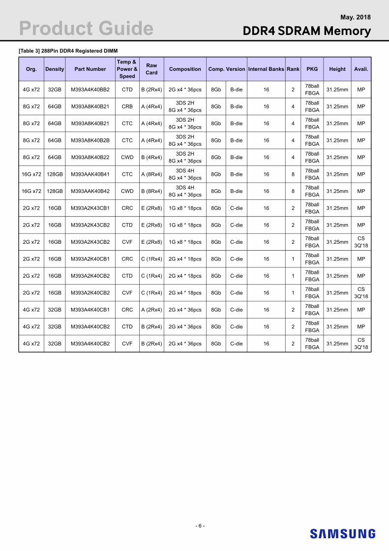
4. DDR4 SDRAM MODULE PRODUCT GUIDE4.1 288Pin DDR4 Registered DIMM
[Table 3] 288Pin DDR4 Registered DIMM
Org. Density Part NumberTemp & Power & Speed
Raw Card
Composition Comp. Version Internal Banks Rank PKG Height Avail.
1G x72 8GB M393A1G40EB1 CPB C (1Rx4) 1G x4 * 18pcs 4Gb E-die 16 178ballFBGA
31.25mmEOL
2Q'18
1G x72 8GB M393A1G40EB1 CRC C (1Rx4) 1G x4 * 18pcs 4Gb E-die 16 178ballFBGA
31.25mmEOL
2Q'18
1G x72 8GB M393A1G40EB2 CTD C (1Rx4) 1G x4 * 18pcs 4Gb E-die 16 178ballFBGA
31.25mmEOL
2Q'18
1G x72 8GB M393A1G43EB1 CPB E (2Rx8) 512G x8 * 18pcs 4Gb E-die 16 278ballFBGA
31.25mmEOL
2Q'18
1G x72 8GB M393A1G43EB1 CRC E (2Rx8) 512G x8 * 18pcs 4Gb E-die 16 278ballFBGA
31.25mmEOL
2Q'18
1G x72 8GB M393A1G43EB1 CTD E (2Rx8) 512G x8 * 18pcs 4Gb E-die 16 278ballFBGA
31.25mmEOL
2Q'18
1G x72 8GB M393A1K43BB0 CPB D (1Rx8) 1G x8 * 9pcs 8Gb B-die 16 178ballFBGA
31.25mm MP
1G x72 8GB M393A1K43BB0 CRC D (1Rx8) 1G x8 * 9pcs 8Gb B-die 16 178ballFBGA
31.25mm MP
1G x72 8GB M393A1K43BB1 CTD D (1Rx8) 1G x8 * 9pcs 8Gb B-die 16 178ballFBGA
31.25mm MP
2G x72 16GB M393A2G40EB1 CPB A (2Rx4) 1G x4 * 36pcs 4Gb E-die 16 278ballFBGA
31.25mmEOL
2Q'18
2G x72 16GB M393A2G40EB1 CRC A (2Rx4) 1G x4 * 36pcs 4Gb E-die 16 278ballFBGA
31.25mmEOL
2Q'18
2G x72 16GB M393A2G40EB2 CTD A (2Rx4) 1G x4 * 36pcs 4Gb E-die 16 278ballFBGA
31.25mmEOL
2Q'18
2G x72 16GB M393A2K43BB1 CPB E (2Rx8) 1G x8 * 18pcs 8Gb B-die 16 278ballFBGA
31.25mm MP
2G x72 16GB M393A2G40EB1 CRC A (2Rx4) 1G x4 * 36pcs 4Gb E-die 16 278ballFBGA
31.25mmEOL
2Q'18
2G x72 16GB M393A2G40EB2 CTD A (2Rx4) 1G x4 * 36pcs 4Gb E-die 16 278ballFBGA
31.25mmEOL
2Q'18
2G x72 16GB M393A2K40BB0 CPB C (1Rx4) 2G x4 * 18pcs 8Gb B-die 16 178ballFBGA
31.25mm MP
2G x72 16GB M393A2K40BB1 CRC C (1Rx4) 2G x4 * 18pcs 8Gb B-die 16 178ballFBGA
31.25mm MP
2G x72 16GB M393A2K40BB2 CTD C (1Rx4) 2G x4 * 18pcs 8Gb B-die 16 178ballFBGA
31.25mm MP
2G x72 16GB M393A2K43BB1 CPB E (2Rx8) 1G x8 * 18pcs 8Gb B-die 16 278ballFBGA
31.25mm MP
2G x72 16GB M393A2K43BB1 CRC E (2Rx8) 1G x8 * 18pcs 8Gb B-die 16 278ballFBGA
31.25mm MP
2G x72 16GB M393A2K43BB1 CTD E (2Rx8) 1G x8 * 18pcs 8Gb B-die 16 278ballFBGA
31.25mm MP
4G x72 32GB M393A4K40BB0 CPB A (2Rx4) 2G x4 * 36pcs 8Gb B-die 16 278ballFBGA
31.25mm MP
4G x72 32GB M393A4K40BB1 CRC A (2Rx4) 2G x4 * 36pcs 8Gb B-die 16 278ballFBGA
31.25mm MP
Page 6
- 6 -
Product Guide DDR4 SDRAM MemoryMay. 2018
4G x72 32GB M393A4K40BB2 CTD B (2Rx4) 2G x4 * 36pcs 8Gb B-die 16 278ballFBGA
31.25mm MP
8G x72 64GB M393A8K40B21 CRB A (4Rx4)3DS 2H
8G x4 * 36pcs8Gb B-die 16 4
78ballFBGA
31.25mm MP
8G x72 64GB M393A8K40B21 CTC A (4Rx4)3DS 2H
8G x4 * 36pcs8Gb B-die 16 4
78ballFBGA
31.25mm MP
8G x72 64GB M393A8K40B2B CTC A (4Rx4)3DS 2H
8G x4 * 36pcs8Gb B-die 16 4
78ballFBGA
31.25mm MP
8G x72 64GB M393A8K40B22 CWD B (4Rx4)3DS 2H
8G x4 * 36pcs8Gb B-die 16 4
78ballFBGA
31.25mm MP
16G x72 128GB M393AAK40B41 CTC A (8Rx4)3DS 4H
8G x4 * 36pcs8Gb B-die 16 8
78ballFBGA
31.25mm MP
16G x72 128GB M393AAK40B42 CWD B (8Rx4)3DS 4H
8G x4 * 36pcs8Gb B-die 16 8
78ballFBGA
31.25mm MP
2G x72 16GB M393A2K43CB1 CRC E (2Rx8) 1G x8 * 18pcs 8Gb C-die 16 278ballFBGA
31.25mm MP
2G x72 16GB M393A2K43CB2 CTD E (2Rx8) 1G x8 * 18pcs 8Gb C-die 16 278ballFBGA
31.25mm MP
2G x72 16GB M393A2K43CB2 CVF E (2Rx8) 1G x8 * 18pcs 8Gb C-die 16 278ballFBGA
31.25mmCS
3Q'18
2G x72 16GB M393A2K40CB1 CRC C (1Rx4) 2G x4 * 18pcs 8Gb C-die 16 178ballFBGA
31.25mm MP
2G x72 16GB M393A2K40CB2 CTD C (1Rx4) 2G x4 * 18pcs 8Gb C-die 16 178ballFBGA
31.25mm MP
2G x72 16GB M393A2K40CB2 CVF C (1Rx4) 2G x4 * 18pcs 8Gb C-die 16 178ballFBGA
31.25mmCS
3Q'18
4G x72 32GB M393A4K40CB1 CRC A (2Rx4) 2G x4 * 36pcs 8Gb C-die 16 278ballFBGA
31.25mm MP
4G x72 32GB M393A4K40CB2 CTD B (2Rx4) 2G x4 * 36pcs 8Gb C-die 16 278ballFBGA
31.25mm MP
4G x72 32GB M393A4K40CB2 CVF B (2Rx4) 2G x4 * 36pcs 8Gb C-die 16 278ballFBGA
31.25mmCS
3Q'18
[Table 3] 288Pin DDR4 Registered DIMM
Org. Density Part NumberTemp & Power & Speed
Raw Card
Composition Comp. Version Internal Banks Rank PKG Height Avail.
Page 7
- 7 -
Product Guide DDR4 SDRAM MemoryMay. 2018
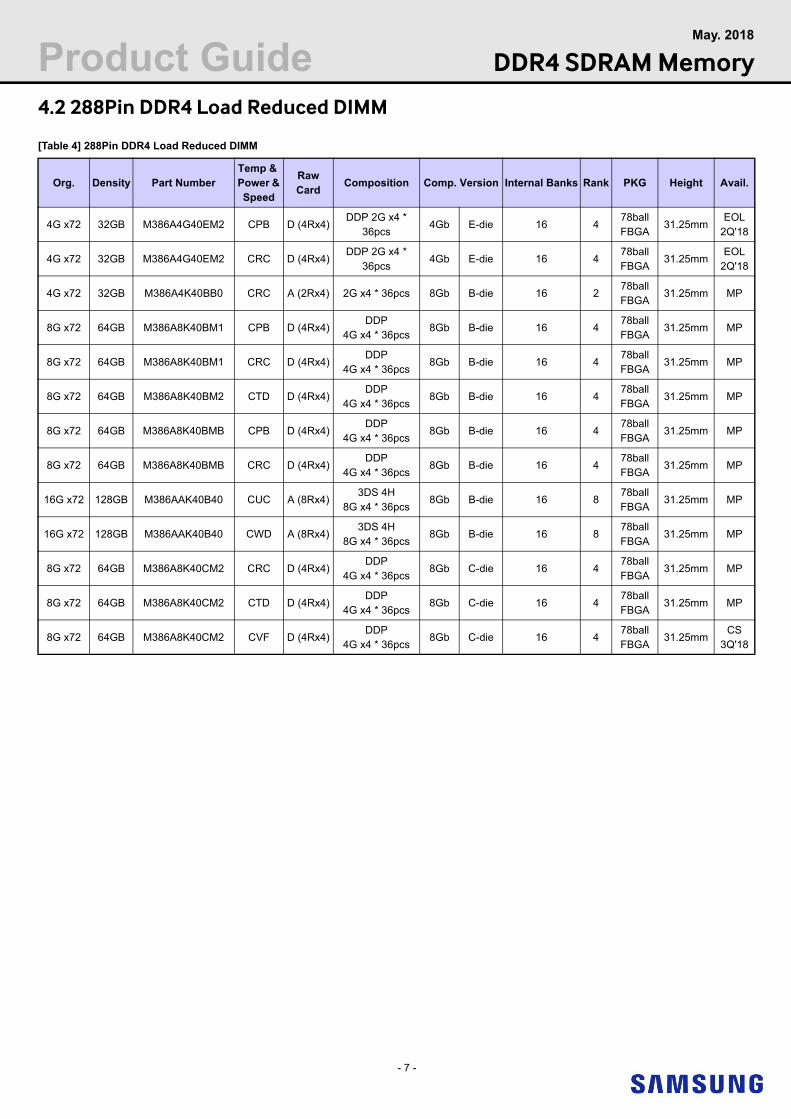
4.2 288Pin DDR4 Load Reduced DIMM
[Table 4] 288Pin DDR4 Load Reduced DIMM
Org. Density Part NumberTemp & Power & Speed
Raw Card
Composition Comp. Version Internal Banks Rank PKG Height Avail.
4G x72 32GB M386A4G40EM2 CPB D (4Rx4)DDP 2G x4 *
36pcs4Gb E-die 16 4
78ballFBGA
31.25mmEOL
2Q'18
4G x72 32GB M386A4G40EM2 CRC D (4Rx4)DDP 2G x4 *
36pcs4Gb E-die 16 4
78ballFBGA
31.25mmEOL
2Q'18
4G x72 32GB M386A4K40BB0 CRC A (2Rx4) 2G x4 * 36pcs 8Gb B-die 16 278ballFBGA
31.25mm MP
8G x72 64GB M386A8K40BM1 CPB D (4Rx4)DDP
4G x4 * 36pcs8Gb B-die 16 4
78ballFBGA
31.25mm MP
8G x72 64GB M386A8K40BM1 CRC D (4Rx4)DDP
4G x4 * 36pcs8Gb B-die 16 4
78ballFBGA
31.25mm MP
8G x72 64GB M386A8K40BM2 CTD D (4Rx4)DDP
4G x4 * 36pcs8Gb B-die 16 4
78ballFBGA
31.25mm MP
8G x72 64GB M386A8K40BMB CPB D (4Rx4)DDP
4G x4 * 36pcs8Gb B-die 16 4
78ballFBGA
31.25mm MP
8G x72 64GB M386A8K40BMB CRC D (4Rx4)DDP
4G x4 * 36pcs8Gb B-die 16 4
78ballFBGA
31.25mm MP
16G x72 128GB M386AAK40B40 CUC A (8Rx4)3DS 4H
8G x4 * 36pcs8Gb B-die 16 8
78ballFBGA
31.25mm MP
16G x72 128GB M386AAK40B40 CWD A (8Rx4)3DS 4H
8G x4 * 36pcs8Gb B-die 16 8
78ballFBGA
31.25mm MP
8G x72 64GB M386A8K40CM2 CRC D (4Rx4)DDP
4G x4 * 36pcs8Gb C-die 16 4
78ballFBGA
31.25mm MP
8G x72 64GB M386A8K40CM2 CTD D (4Rx4)DDP
4G x4 * 36pcs8Gb C-die 16 4
78ballFBGA
31.25mm MP
8G x72 64GB M386A8K40CM2 CVF D (4Rx4)DDP
4G x4 * 36pcs8Gb C-die 16 4
78ballFBGA
31.25mmCS
3Q'18
Page 8
- 8 -
Product Guide DDR4 SDRAM MemoryMay. 2018
4.3 288Pin DDR4 VLP Registered DIMM
[Table 5] 288Pin DDR4 VLP Registered DIMM
Org. Density Part NumberTemp & Power & Speed
Raw Card
Composition Comp. Version Internal Banks Rank PKG Height Avail.
2G x72 16GB M392A2K43BB0 CPB H (2Rx8) 1G x8 * 18pcs 8Gb B-die 16 278ballFBGA
18.75mm MP
2G x72 16GB M392A2K43BB0 CRC H (2Rx8) 1G x8 * 18pcs 8Gb B-die 16 278ballFBGA
18.75mm MP
4G x72 32GB M392A4K40BM0 CPB J (2Rx4) 4G x4 * 18pcs 8Gb B-die 16 278ballFBGA
18.75mm MP
4G x72 32GB M392A4K40BM0 CRC J (2Rx4) 4G x4 * 18pcs 8Gb B-die 16 278ballFBGA
18.75mm MP
4.4 260Pin DDR4 ECC SODIMM
[Table 6] 260Pin DDR4 ECC SODIMM
Org. Density Part NumberTemp & Power & Speed
Raw Card
Composition Comp. Version Internal Banks Rank PKG Height Avail.
1G x72 8GB M474A1G43EB1 CPB G (2Rx8) 512M x8 * 18pcs 4Gb E-die 16 278ballFBGA
30mmEOL
2Q'18
1G x72 8GB M474A1G43EB1 CRC G (2Rx8) 512M x8 * 18pcs 4Gb E-die 16 278ballFBGA
30mmEOL
2Q'18
1G x72 8GB M474A1K43BB1 CTD D (1Rx8) 1G x8 * 9pcs 8Gb B-die 16 178ballFBGA
30mm MP
2G x72 16GB M474A2K43BB1 CPB G (2Rx8) 1G x8 * 18pcs 8Gb B-die 16 278ballFBGA
30mm MP
2G x72 16GB M474A2K43BB1 CRC G (2Rx8) 1G x8 * 18pcs 8Gb B-die 16 278ball
FBGA30mm MP
2G x72 16GB M474A2K43BB1 CTD G (2Rx8) 1G x8 * 18pcs 8Gb B-die 16 278ballFBGA
30mm MP
Page 9
- 9 -
Product Guide DDR4 SDRAM MemoryMay. 2018
4.5 260Pin DDR4 ECC UDIMM
[Table 7] 260Pin DDR4 ECC UDIMM
Org. Density Part NumberTemp & Power & Speed
Raw Card
Composition Comp. Version Internal Banks Rank PKG Height Avail.
512M x72 4GB M391A5143EB1 CPB D (1Rx8) 512M x8 * 9pcs 4Gb E-die 16 178ballFBGA
31.25mmEOL
2Q'18
512M x72 4GB M391A5143EB1 CRC D (1Rx8) 512M x8 * 9pcs 4Gb E-die 16 178ballFBGA
31.25mmEOL
2Q'18
1G x72 8GB M391A1G43EB1 CPB E (2Rx8) 512M x8 * 18pcs 4Gb E-die 16 278ballFBGA
31.25mmEOL
2Q'18
1G x72 8GB M391A1G43EB1 CRC E (2Rx8) 512M x8 * 18pcs 4Gb E-die 16 278ballFBGA
31.25mmEOL
2Q'18
1G x72 8GB M391A1K43BB1 CPB D (1Rx8) 1G x8 * 9pcs 8Gb B-die 16 178ballFBGA
31.25mm MP
1G x72 8GB M391A1K43BB1 CRC D (1Rx8) 1G x8 * 9pcs 8Gb B-die 16 178ballFBGA
31.25mm MP
1G x72 8GB M391A1K43BB2 CTD D (1Rx8) 1G x8 * 9pcs 8Gb B-die 16 178ballFBGA
31.25mm MP
2G x72 16GB M391A2K43BB1 CPB E (2Rx8) 1G x8 * 18pcs 8Gb B-die 16 278ballFBGA
31.25mm MP
2G x72 16GB M391A2K43BB1 CRC E (2Rx8) 1G x8 * 18pcs 8Gb B-die 16 278ballFBGA
31.25mm MP
2G x72 16GB M391A2K43BB1 CTD E (2Rx8) 1G x8 * 18pcs 8Gb B-die 16 278ballFBGA
31.25mm MP
Page 10
- 10 -
Product Guide DDR4 SDRAM MemoryMay. 2018
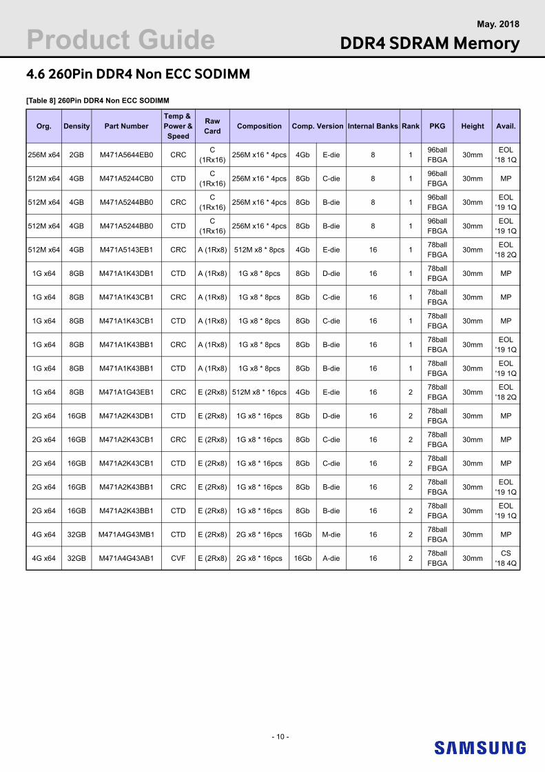
4.6 260Pin DDR4 Non ECC SODIMM
[Table 8] 260Pin DDR4 Non ECC SODIMM
Org. Density Part NumberTemp & Power & Speed
Raw Card
Composition Comp. Version Internal Banks Rank PKG Height Avail.
256M x64 2GB M471A5644EB0 CRCC
(1Rx16)256M x16 * 4pcs 4Gb E-die 8 1
96ball FBGA
30mmEOL
'18 1Q
512M x64 4GB M471A5244CB0 CTDC
(1Rx16)256M x16 * 4pcs 8Gb C-die 8 1
96ball FBGA
30mm MP
512M x64 4GB M471A5244BB0 CRCC
(1Rx16)256M x16 * 4pcs 8Gb B-die 8 1
96ball FBGA
30mmEOL
'19 1Q
512M x64 4GB M471A5244BB0 CTDC
(1Rx16)256M x16 * 4pcs 8Gb B-die 8 1
96ball FBGA
30mmEOL
'19 1Q
512M x64 4GB M471A5143EB1 CRC A (1Rx8) 512M x8 * 8pcs 4Gb E-die 16 178ball FBGA
30mmEOL
'18 2Q
1G x64 8GB M471A1K43DB1 CTD A (1Rx8) 1G x8 * 8pcs 8Gb D-die 16 178ball FBGA
30mm MP
1G x64 8GB M471A1K43CB1 CRC A (1Rx8) 1G x8 * 8pcs 8Gb C-die 16 178ball FBGA
30mm MP
1G x64 8GB M471A1K43CB1 CTD A (1Rx8) 1G x8 * 8pcs 8Gb C-die 16 178ball FBGA
30mm MP
1G x64 8GB M471A1K43BB1 CRC A (1Rx8) 1G x8 * 8pcs 8Gb B-die 16 178ball FBGA
30mmEOL
'19 1Q
1G x64 8GB M471A1K43BB1 CTD A (1Rx8) 1G x8 * 8pcs 8Gb B-die 16 178ball FBGA
30mmEOL
'19 1Q
1G x64 8GB M471A1G43EB1 CRC E (2Rx8) 512M x8 * 16pcs 4Gb E-die 16 278ball FBGA
30mmEOL
'18 2Q
2G x64 16GB M471A2K43DB1 CTD E (2Rx8) 1G x8 * 16pcs 8Gb D-die 16 278ball FBGA
30mm MP
2G x64 16GB M471A2K43CB1 CRC E (2Rx8) 1G x8 * 16pcs 8Gb C-die 16 278ball FBGA
30mm MP
2G x64 16GB M471A2K43CB1 CTD E (2Rx8) 1G x8 * 16pcs 8Gb C-die 16 278ball FBGA
30mm MP
2G x64 16GB M471A2K43BB1 CRC E (2Rx8) 1G x8 * 16pcs 8Gb B-die 16 278ball FBGA
30mmEOL
'19 1Q
2G x64 16GB M471A2K43BB1 CTD E (2Rx8) 1G x8 * 16pcs 8Gb B-die 16 278ball FBGA
30mmEOL
'19 1Q
4G x64 32GB M471A4G43MB1 CTD E (2Rx8) 2G x8 * 16pcs 16Gb M-die 16 278ball FBGA
30mm MP
4G x64 32GB M471A4G43AB1 CVF E (2Rx8) 2G x8 * 16pcs 16Gb A-die 16 278ball FBGA
30mmCS
'18 4Q
Page 11
- 11 -
Product Guide DDR4 SDRAM MemoryMay. 2018
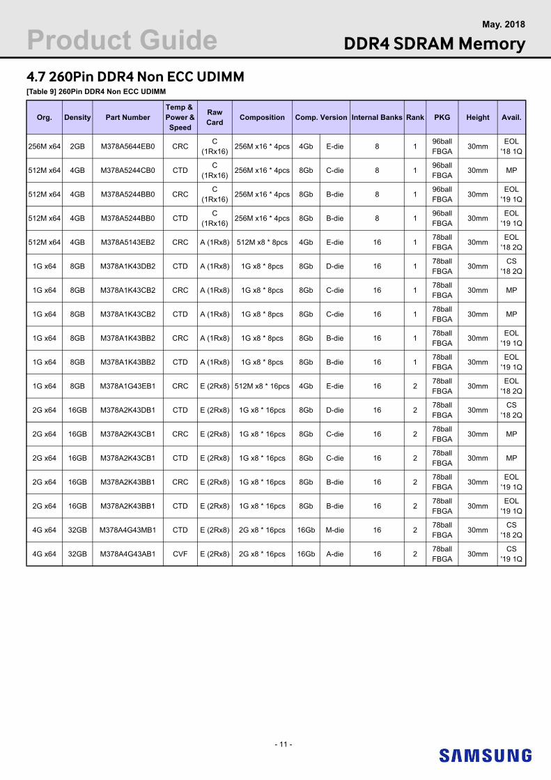
4.7 260Pin DDR4 Non ECC UDIMM[Table 9] 260Pin DDR4 Non ECC UDIMM
Org. Density Part NumberTemp & Power & Speed
Raw Card
Composition Comp. Version Internal Banks Rank PKG Height Avail.
256M x64 2GB M378A5644EB0 CRCC
(1Rx16)256M x16 * 4pcs 4Gb E-die 8 1
96ball FBGA
30mmEOL
'18 1Q
512M x64 4GB M378A5244CB0 CTDC
(1Rx16)256M x16 * 4pcs 8Gb C-die 8 1
96ball FBGA
30mm MP
512M x64 4GB M378A5244BB0 CRCC
(1Rx16)256M x16 * 4pcs 8Gb B-die 8 1
96ball FBGA
30mmEOL
'19 1Q
512M x64 4GB M378A5244BB0 CTDC
(1Rx16)256M x16 * 4pcs 8Gb B-die 8 1
96ball FBGA
30mmEOL
'19 1Q
512M x64 4GB M378A5143EB2 CRC A (1Rx8) 512M x8 * 8pcs 4Gb E-die 16 178ball FBGA
30mmEOL
'18 2Q
1G x64 8GB M378A1K43DB2 CTD A (1Rx8) 1G x8 * 8pcs 8Gb D-die 16 178ball FBGA
30mmCS
'18 2Q
1G x64 8GB M378A1K43CB2 CRC A (1Rx8) 1G x8 * 8pcs 8Gb C-die 16 178ball FBGA
30mm MP
1G x64 8GB M378A1K43CB2 CTD A (1Rx8) 1G x8 * 8pcs 8Gb C-die 16 178ball FBGA
30mm MP
1G x64 8GB M378A1K43BB2 CRC A (1Rx8) 1G x8 * 8pcs 8Gb B-die 16 178ball FBGA
30mmEOL
'19 1Q
1G x64 8GB M378A1K43BB2 CTD A (1Rx8) 1G x8 * 8pcs 8Gb B-die 16 178ball FBGA
30mmEOL
'19 1Q
1G x64 8GB M378A1G43EB1 CRC E (2Rx8) 512M x8 * 16pcs 4Gb E-die 16 278ball FBGA
30mmEOL
'18 2Q
2G x64 16GB M378A2K43DB1 CTD E (2Rx8) 1G x8 * 16pcs 8Gb D-die 16 278ball FBGA
30mmCS
'18 2Q
2G x64 16GB M378A2K43CB1 CRC E (2Rx8) 1G x8 * 16pcs 8Gb C-die 16 278ball FBGA
30mm MP
2G x64 16GB M378A2K43CB1 CTD E (2Rx8) 1G x8 * 16pcs 8Gb C-die 16 278ball FBGA
30mm MP
2G x64 16GB M378A2K43BB1 CRC E (2Rx8) 1G x8 * 16pcs 8Gb B-die 16 278ball FBGA
30mmEOL
'19 1Q
2G x64 16GB M378A2K43BB1 CTD E (2Rx8) 1G x8 * 16pcs 8Gb B-die 16 278ball FBGA
30mmEOL
'19 1Q
4G x64 32GB M378A4G43MB1 CTD E (2Rx8) 2G x8 * 16pcs 16Gb M-die 16 278ball FBGA
30mmCS
'18 2Q
4G x64 32GB M378A4G43AB1 CVF E (2Rx8) 2G x8 * 16pcs 16Gb A-die 16 278ball FBGA
30mmCS
'19 1Q
Page 12
- 12 -
Product Guide DDR4 SDRAM MemoryMay. 2018
5. RDIMM, LRDIMM Memory Buffer Information
5.1 Label Example
64GB 4Rx4 PC4 -2400T-LD1-11
Country M386A8K40BM1-CRC5Q
C2AHA40633333C78B3 YYWW
1 2 3 4 5 6 7 8 9 10
5.2 JEDEC Description Information
1. Module total capacity, in gigabytes, for primary bus (ECC not counted)2. Number of package ranks of memory installed and number of logical ranks per package rank3. Device organization (data bit width) of SDRAMs used on this assembly
4. SDRAM and support component supply voltage (VDD) blank = 1.2 V operable5. Module speed in Mb/s/data pin6. SDRAM speed grade7. Module Type A = Unbuffered 16-bit Small Outline DIMM (“16b-SO-DIMM”), x16 data bus (placeholder) B = Unbuffered 32-bit Small Outline DIMM (“32b-SO-DIMM”), x32 data bus (placeholder) C = Registered 72-bit Small Outline DIMM ("72b-SO-RDIMM”), x64 primary + 8 bit ECC module data bus(placeholder) E = Unbuffered DIMM ("UDIMM"), x64 primary + 8 bit ECC module data bus L = Load Reduced DIMM (“LRDIMM”), x64 primary + 8 bit ECC module data bus N = Mini registered DIMM (“Mini-RDIMM”), x64 primary + 8 bit ECC module data bus R = Registered DIMM ("RDIMM"), x64 primary + 8 bit ECC module data bus S = Small Outline DIMM ("SO-DIMM"), no ECC (x64 bit module data bus) T = Unbuffered 72-bit Small Outline DIMM ("72b-SO-DIMM"), x64 primary + 8 bit ECC module data bus U = Unbuffered DIMM ("UDIMM"), no ECC (x64 bit module data bus) W = Mini unbuffered DIMM ("Mini-UDIMM"), x64 primary + 8 bit ECC module data bus
8. Reference design file used for this design (if applicable) A = Reference design for raw card ’A’ is used for this assembly B = Reference design for raw card ’B’ is used for this assembly AC = Reference design for raw card ’AC’ is used for this assembly (example only) ZZ = None of the JEDEC standard reference designs were used for this assembly
9. Revision number of the reference design used 0 = Initial release 1 = First revision 2 = Second revision P = Pre-release or Engineering sample Z = To be used when reference raw card = ZZ10. JEDEC SPD Revision Encoding and Additions level used on this DIMM
Page 13
- 13 -
Product Guide DDR4 SDRAM MemoryMay. 2018
5.3 RCD (& Data Buffer) Information (These codes are only used SAMSUNG, Not JEDEC)
11&12. RCD, Data Buffer Revision & Vendor used on this DIMM
Jedec Description on label Buffer Vendor RCD ver DB ver (Only LRDIMM)
DC0 IDT C0 B1
MB1 Montage B1 A1
MC0 Montage C0 B0
DC3 IDT C0 A3
MA0 Montage A0 A1
DB1 IDT B1 B0
PA0 Rambus (Inphi) A0 A0
DC1 IDT C1 C1
Page 14
- 14 -
Product Guide DDR4 SDRAM MemoryMay. 2018
6. PACKAGE DIMENSION
78ball FBGA for 4Gb D-die (x4/x8) / DDP 8Gb D-die (x4) / 4H 16Gb D-die (x4)
4Gb E-die (x4/x8)8Gb B-die (x4/x8) / DDP 16Gb B-die (x4) / 2H 16Gb B-die (x4) / 4H 32Gb B-die (x4)8Gb C-die (x4/x8)
A
B
C
D
E
F
G
H
M
N
7.50 0.10
0.8
0 x1
2 =
9.6
0
3.200.804
.80
78 - Æ0.48 Solder ball
0.2 A BM
(Datum B)
(Datum A) 0.1
0M
AX
1.10 0.10
#A1 1.60
7.50 0.10
11.0
0 0
.10
0.37 0.05
#A1 INDEX MARK
B
A
BOTTOM VIEW TOP VIEW
11.0
0
0.1
0
J
K
L 0.8
00
.80
(Post Reflow Æ0.50 ± 0.05)
8 7 6 5 4 3 2 19
0.80 x 8 6.40
Page 15
- 15 -
Product Guide DDR4 SDRAM MemoryMay. 2018
78ball FBGA for 16Gb M-die (x4/x8)
ABCDEFGH
MN
0.8
0 x1
2 =
9.6
0
3.20
4.8
0
78 - 0.48 Solder ball
0.1
0MA
X
1.10 0.10
#A1
1.60
10.30 0.10
11.0
0
0.1
0
0.37 0.05
#A1 INDEX MARK
BA
BOTTOM VIEW TOP VIEW
JKL 0
.80
(Post Reflow 0.50 ± 0.05)
8 7 6 5 4 3 2 19
0.80 x 8 6.40
0.20 M A B
A A’
0.8
0
0.80
0.30
0.60
C
0.2
0 M
AX
MOLDING COMPOUND
SIDE VIEW
SECTION A-A’
Page 16
- 16 -
Product Guide DDR4 SDRAM MemoryMay. 2018
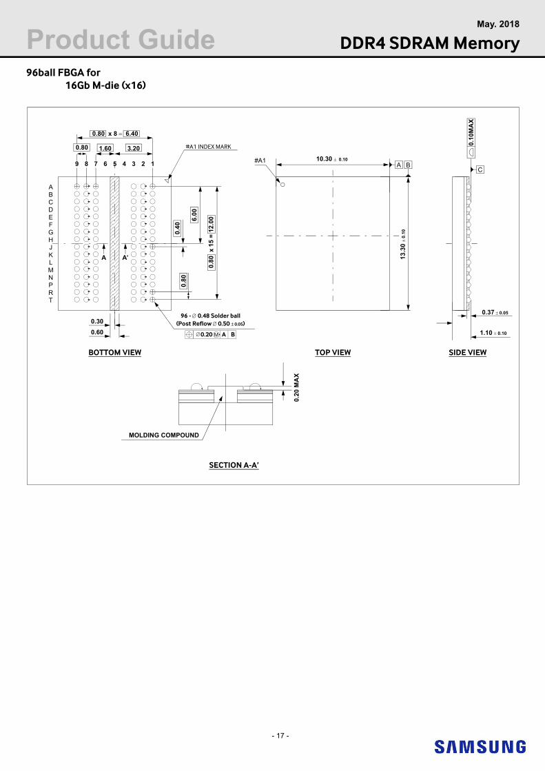
96ball FBGA for 4Gb D-die (x16) / 4Gb E-die (x16)8Gb B-die (x16) / 8Gb C-die (x16)
BOTTOM VIEW
A
B
C
D
E
F
G
H
M
N
0.8
0 x1
5 =
12.0
0
3.200.80
(Datum B)
(Datum A)1.60
MOLDING AREA
#A1 INDEX MARK
B
13.3
0 0
.10
J
K
L
0.8
00.4
0
(Post reflow 0.50 ± 0.05)
(0.30)
(0.60)
8 7 6 5 4 3 2 19
x 8 = 6.40
A
0.80
7.50 0.10
R
T
P
0.2 A BM
96 - 0.48 Solder ball
0.1
0M
AX
1.10 0.10
#A1 7.50 0.10
13.
30 0
.10
0.37 0.05
TOP VIEW
Page 17
- 17 -
Product Guide DDR4 SDRAM MemoryMay. 2018
96ball FBGA for 16Gb M-die (x16)
ABCDEFGH
MN
0.8
0
x1
5 =
12
.00
3.20
6.0
0
96 - 0.48 Solder ball
0.1
0MA
X
1.10 0.10
#A1
1.60
10.30 0.10
13
.30
0
.10
0.37 0.05
#A1 INDEX MARK
BA
BOTTOM VIEW TOP VIEW
JKL
0.8
0
(Post Reflow 0.50 ± 0.05)
8 7 6 5 4 3 2 19
0.80 x 8 6.40
0.20 M A B
A A’
0.4
0
0.80
0.30
0.60
C
0.2
0 M
AX
MOLDING COMPOUND
SIDE VIEW
SECTION A-A’
PRT
Page 18
- 18 -
Product Guide DDR4 SDRAM MemoryMay. 2018
7. MODULE DIMENSIONx72 288pin DDR4 SDRAM RDIMMx72 288pin DDR4 SDRAM LRDIMMx72 288pin DDR4 SDRAM ECC UDIMMx64 288pin DDR4 SDRAM Non ECC UDIMM
133.35
Units : Millimeters
31.2
5
30.7
5
17.
60
126.65
56.1064.60 3.35
AC E D B
Detail A
1.50 ± 0.05
3.85 ± 0.10
4.30
0.85
0.25
E :
2.6
Detail B,E
0.6 ± 0.03
B :
2.1
Detail C
2.1
9.3510.20
2.6 2.1
9.3510.20
2.6
Detail D
1.4 ± 0.10
Max 1.4
Max 1.4
Page 19
- 19 -
Product Guide DDR4 SDRAM MemoryMay. 2018
x72 260pin DDR4 SDRAM ECC SODIMMx64 260pin DDR4 SDRAM Non ECC SODIMM
0.30 MAX
2.55
Detail BDetail A
1.00 ± 0.05
0.35 ± 0.03
4.00 ± 0.10
0.50
Units : Millimeters
35.50 28.50
A B
1.375
30
.00
69.60
65.60Max 3.7
1.2 ± 0.10
Page 20
- 20 -
Product Guide DDR4 SDRAM MemoryMay. 2018
x72 288pin DDR4 SDRAM VLP RDIMM
133.35
Units : Millimeters
Reg
iste
r
1.4 ± 0.10
0.85
0.25
E :
2.6
Detail B,E
Detail A
1.50 ± 0.05
0.6 ± 0.03
3.85 ± 0.10
Detail C18
.75
Max 4.9
18.2
5
126.65
4.30
B :
2.1
2.1
9.3510.20
2.6 2.1
9.3510.20
2.6
Detail D
56.1064.60
AC E D B
Page 21
- 21 -
Product Guide DDR4 SDRAM MemoryMay. 2018
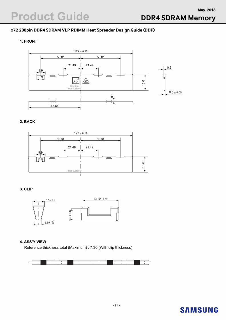
x72 288pin DDR4 SDRAM VLP RDIMM Heat Spreader Design Guide (DDP)
1. FRONT
13.
6
127 ± 0.12
50.81
21.49
9.9
8.9
21.49
50.81
0.6
63.68
Caution"Hot surface"
3. CLIP
9.3
± 0
.12
35.82 ± 0.126.8 ± 0.1
3.80+0.5-0.8
0.8 ± 0.05
0.6
2. BACK
13.6
127 ± 0.12
50.81
21.49
9.9
8.9
21.49
50.81
"Hot surface"
4. ASS’Y VIEW
Reference thickness total (Maximum) : 7.30 (With clip thickness)
Page 22
- 22 -
Product Guide DDR4 SDRAM MemoryMay. 2018
x72 288pin DDR4 SDRAM RDIMM Heat Spreader Design Guide (TSV)
133.15 ± 0.2
130.45 ± 0.2
127 ± 0.12
25.7
5 ±
0.15
2.6
± 0
.2
1. FRONT PART
2. BACK PART
19.
25
± 0.
12
39.3 ± 0.27 ± 0.12
Clip open size
3.2 ± 0.6
3. CLIP PART
0.6
± 0
.12
31.1 ± 0.12 17.02 ± 0.125.785 ± 0.12
4.35
± 0
.12
6.075 ± 0.12
Page 23
- 23 -
Product Guide DDR4 SDRAM MemoryMay. 2018
x72 288pin DDR4 SDRAM LRDIMM Heat Spreader Design Guide (DDP)
133.15
130.45 ± 0.2
127 ± 0.25
25.7
5 ±
0.2
2.8
± 0
.2
1. FRONT PART
2. BACK PART
19.2
5 ±
0.1
2
39.3 ± 0.2
7 ± 0.12
Clip open size3.2 ± 0.6
3. CLIP PART
+0.40-0.20
18.6
± 0
.25
0.6
± 0
.1


![8Gb C-die DDR4 SDRAM x16 - samsung.com · - 5 - datasheet DDR4 SDRAM Rev.1.5 K4A8G165WC 1. Ordering Information [ Table 1 ] Samsung 8Gb DDR4 C-die ordering information table NOTE:](https://static.documents.pub/doc/80x56/5dd0e855d6be591ccb6347b7/8gb-c-die-ddr4-sdram-x16-5-datasheet-ddr4-sdram-rev15-k4a8g165wc-1-ordering.jpg)


![8Gb B-die DDR4 SDRAM · - 5 - K4A8G085WB datasheet DDR4 SDRAM K4A8G045WB Rev. 2.1 1. Ordering Information [ Table 1 ] Samsung 8Gb DDR4 B-die Ordering Information Table NOTE: 1. Speed](https://static.documents.pub/doc/80x56/5d6717c388c993d50c8b9d19/8gb-b-die-ddr4-sdram-5-k4a8g085wb-datasheet-ddr4-sdram-k4a8g045wb-rev-21.jpg)


