management integrated in single module– Persistent energy source options
• Option 1: Battery-free power source (Power-GEM)
• Option 2: Persistent DDR4 12V pin– 32GB (4 Gig x 72) DDR4 RDIMM– 64GB SLC Flash– DDR4 functionality and operations supported as
defined in the component data sheet– JEDEC compliant DDR4 288-pin dual in-line
memory module connector– Fast data transfer rate: PC4-2933– VDD = 1.20V (typical)– VPP = 2.5V (typical)– VDDSPD = 2.2–2.8V– Supports ECC error detection and correction– Nominal and dynamic on-die termination (ODT)
for data, strobe, and mask signals– Low-power auto self refresh (LPASR)– On-die VREFDQ generation and calibration– Dual-rank, comprised of TwinDie™, x4 DRAM
components– On-board I2C temperature sensor with integrated
serial presence-detect (SPD) EEPROM– 16 internal banks; 4 groups of 4 banks each– Fixed burst chop (BC) of 4 and burst length (BL)
of 8 via the mode register set (MRS)– Selectable BC4 or BL8 on-the-fly (OTF)– Gold edge contacts– Halogen-free– Fly-by topology– Terminated control, command, and address bus
• Battery-free power source (ultra capacitor basedPowerGEM)– Powers the Micron NVDIMM when the host sys-
tem loses power– 5-year operating life– 0°C to 55°C operating range (standard)– No catastrophic failure modes– RoHS-, REACH-, and UL-compliant
• Nonvolatile memory (NVM) system-level features– In-system health monitoring of PowerGEM and
NF– Automatic history tracking: tracks critical inter-
nal system parameters– Interlocked control sequence for safe and reliable
CCM005-341111752-10449ass36c4gx72xf1z.pdf - Rev. A 11/17 EN 1 Micron Technology, Inc. reserves the right to change products or specifications without notice.
Notes: 1. The data sheet for the base device can be found on micron.com.2. All NVDIMM part numbers end with a five-character code (not shown) that designates die revision, PCB revi-
sion and controller type. Consult factory for current revision/controller codes. Example:MTA36ASS4G72XF1Z-2G69PR1AB.
CCM005-341111752-10449ass36c4gx72xf1z.pdf - Rev. A 11/17 EN 2 Micron Technology, Inc. reserves the right to change products or specifications without notice.
Micron Technology, Inc. ("Micron") reserves the right to make changes to information published in this document,including without limitation specifications and product descriptions. This document supersedes and replaces allinformation supplied prior to the publication hereof. You may not rely on any information set forth in this docu-ment if you obtain the product described herein from any unauthorized distributor or other source not authorizedby Micron.
Automotive Applications. Products are not designed or intended for use in automotive applications unless specifi-cally designated by Micron as automotive-grade by their respective data sheets. Distributor and customer/distrib-utor shall assume the sole risk and liability for and shall indemnify and hold Micron harmless against all claims,costs, damages, and expenses and reasonable attorneys' fees arising out of, directly or indirectly, any claim ofproduct liability, personal injury, death, or property damage resulting directly or indirectly from any use of non-automotive-grade products in automotive applications. Customer/distributor shall ensure that the terms and con-ditions of sale between customer/distributor and any customer of distributor/customer (1) state that Micronproducts are not designed or intended for use in automotive applications unless specifically designated by Micronas automotive-grade by their respective data sheets and (2) require such customer of distributor/customer to in-demnify and hold Micron harmless against all claims, costs, damages, and expenses and reasonable attorneys'fees arising out of, directly or indirectly, any claim of product liability, personal injury, death, or property damageresulting from any use of non-automotive-grade products in automotive applications.
Critical Applications. Products are not authorized for use in applications in which failure of the Micron compo-nent could result, directly or indirectly in death, personal injury, or severe property or environmental damage("Critical Applications"). Customer must protect against death, personal injury, and severe property and environ-mental damage by incorporating safety design measures into customer's applications to ensure that failure of theMicron component will not result in such harms. Should customer or distributor purchase, use, or sell any Microncomponent for any critical application, customer and distributor shall indemnify and hold harmless Micron andits subsidiaries, subcontractors, and affiliates and the directors, officers, and employees of each against all claims,costs, damages, and expenses and reasonable attorneys' fees arising out of, directly or indirectly, any claim ofproduct liability, personal injury, or death arising in any way out of such critical application, whether or not Mi-cron or its subsidiaries, subcontractors, or affiliates were negligent in the design, manufacture, or warning of theMicron product.
Customer Responsibility. Customers are responsible for the design, manufacture, and operation of their systems,applications, and products using Micron products. ALL SEMICONDUCTOR PRODUCTS HAVE INHERENT FAIL-URE RATES AND LIMITED USEFUL LIVES. IT IS THE CUSTOMER'S SOLE RESPONSIBILITY TO DETERMINEWHETHER THE MICRON PRODUCT IS SUITABLE AND FIT FOR THE CUSTOMER'S SYSTEM, APPLICATION, ORPRODUCT. Customers must ensure that adequate design, manufacturing, and operating safeguards are includedin customer's applications and products to eliminate the risk that personal injury, death, or severe property or en-vironmental damages will result from failure of any semiconductor component.
Limited Warranty. In no event shall Micron be liable for any indirect, incidental, punitive, special or consequentialdamages (including without limitation lost profits, lost savings, business interruption, costs related to the removalor replacement of any products or rework charges) whether or not such damages are based on tort, warranty,breach of contract or other legal theory, unless explicitly stated in a written agreement executed by Micron's dulyauthorized representative.
CCM005-341111752-10449ass36c4gx72xf1z.pdf - Rev. A 11/17 EN 3 Micron Technology, Inc. reserves the right to change products or specifications without notice.
NVDIMM System Block DiagramThis Micron NVDIMM is available as a 288-pin DDR4 RDIMM with a 72-bit wide databus in dual rank x4 configuration, using 16Gb TwinDie DRAM components for 32GBDRAM density.
Figure 2: Micron DDR4 NVDIMM System Block Diagram
288-pin DDR4 Registerd NVDIMM
SDR
AM
Reg
iste
r
MUXNVDIMMController
CSAVESMBSlave
NANDFlash
PowerManagement
Option 1
Option 2
BackupEnergySource
SystemPowerSupply
DDR4
Host
SMB master
SPD interface
SAVE_nor
RESET_n 1.2V/12V
A persistent energy source ensures continuity of power to the Micron NVDIMM afterthe system power supply is interrupted. This enables the NVDIMM to save the contentsof the DDR4 SDRAM to the nonvolatile NAND Flash memory and shut down independ-ently from the system's power supply.
The persistent energy source can be provided to the NVDIMM in one of two ways:
• Option 1 - PowerGEM (green energy module): Designed by Agiga Tech®, this ultraca-pacitor-based energy source is connected to the Micron NVDIMM via a proprietarycable and connection, providing backup power as well as health monitoring features.The ultracaps are charged through the 12V power pin on the DDR4 connector. Pleaserefer to the Ultracapacitor Power Module data sheet available from micron.com forfurther information.
• Option 2 - Backup Energy Source: Consists of a rechargeable energy source providedby the system. After power interruption, the persistent 12V power pin on the JEDECcompliant DDR4 DIMM connector supplies the power needed to backup the datafrom the DDR4 SDRAM to the NAND Flash. Implementation of this option requiresfurther system design. Without implementation of the PowerGEM, health monitoringand power management become dependent on the system design.
Host Coordination Using Micron NVDIMM Control SignalTo prevent SDRAM data corruption due to a sudden power failure, the host must takesteps to ensure the SDRAM is placed in a safe state as soon as a power failure has beendetected.
CCM005-341111752-10449ass36c4gx72xf1z.pdf - Rev. A 11/17 EN 4 Micron Technology, Inc. reserves the right to change products or specifications without notice.
The Micron NVDIMM will be able to provide proper coordination if the host meets thefollowing requirements:
• The host must have early warning that power is failing, allowing it to perform an or-derly shutdown. Typically, this is achieved by the system monitoring the system pow-er supply and providing a signal that indicates power is failing.
• The host must put the DDR4 SDRAM into self refresh before handing it off to the Mi-cron NVDIMM subsystem. After this state is entered, the clock enable (CKE0) signal isLOW and all SDRAM control signals except CKE0 and RESET_n are "Don't Care." TheSDRAM refreshes itself in this mode, preserving its contents as the host triggers theNVDIMM to take control of the SDRAM, and the SDRAM contents are backed up tothe Flash memory.
• When the host regains control of the DDR4 SDRAM from the Micron NVDIMM con-troller (for example, after performing a FORCE_RESTORE operation), the host mustremove the DDR4 SDRAM from self refresh. The host should take care not to assertthe RESET_n signal after a FORCE_RESTORE operation completes, as the RESET_nsignal resets the internal SDRAM state machine and restored data can be potentiallylost.
For more detailed information regarding host coordination with the Micron NVDIMMcontroller, refer to the Micron NVDIMM firmware specification.
32GB (x72, ECC,TwinDie DR) 288-Pin DDR4 Nonvolatile RDIMMHost Coordination Using Micron NVDIMM Control Signal
CCM005-341111752-10449ass36c4gx72xf1z.pdf - Rev. A 11/17 EN 5 Micron Technology, Inc. reserves the right to change products or specifications without notice.
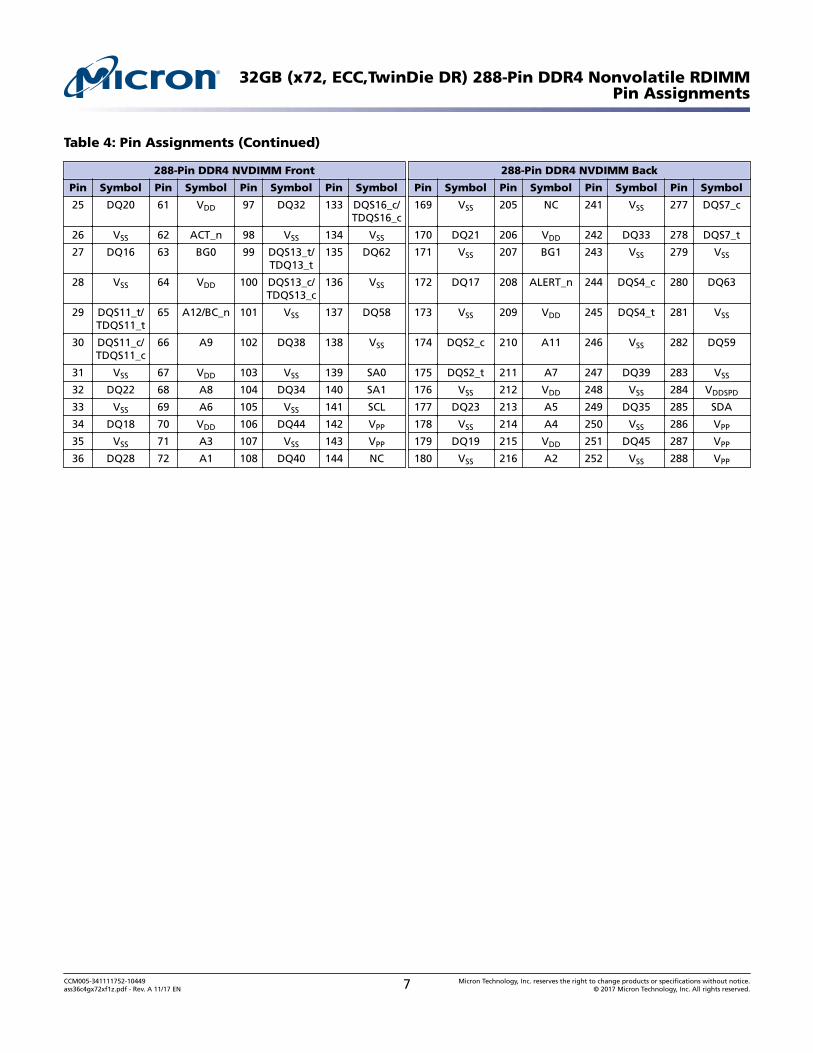
Pin AssignmentsThe pin assignment table below is a comprehensive list of all possible pin assignmentsfor DDR4 RDIMM modules. See the Functional Block Diagram for pins specific to thismodule.
Table 4: Pin Assignments
288-Pin DDR4 NVDIMM Front 288-Pin DDR4 NVDIMM Back
Pin Symbol Pin Symbol Pin Symbol Pin Symbol Pin Symbol Pin Symbol Pin Symbol Pin Symbol
CCM005-341111752-10449ass36c4gx72xf1z.pdf - Rev. A 11/17 EN 6 Micron Technology, Inc. reserves the right to change products or specifications without notice.
CCM005-341111752-10449ass36c4gx72xf1z.pdf - Rev. A 11/17 EN 7 Micron Technology, Inc. reserves the right to change products or specifications without notice.
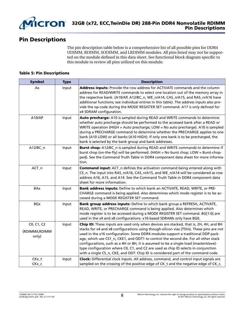
Pin DescriptionsThe pin description table below is a comprehensive list of all possible pins for DDR4UDIMM, RDIMM, SODIMM, and LRDIMM modules. All pins listed may not be suppor-ted on the module defined in this data sheet. See functional block diagram specific tothis module to review all pins utilized on this module.
Table 5: Pin Descriptions
Symbol Type Description
Ax Input Address inputs: Provide the row address for ACTIVATE commands and the columnaddress for READ/WRITE commands to select one location out of the memory array inthe respective bank. (A10/AP, A12/BC_n, WE_n/A14, CAS_n/A15, and RAS_n/A16 haveadditional functions; see individual entries in this table). The address inputs also pro-vide the op-code during the MODE REGISTER SET command. A17 is only defined forx4 SDRAM configuration.
A10/AP Input Auto precharge: A10 is sampled during READ and WRITE commands to determinewhether auto precharge should be performed to the accessed bank after a READ orWRITE operation (HIGH = Auto precharge; LOW = No auto precharge). A10 is sampledduring a PRECHARGE command to determine whether the PRECHARGE applies to onebank (A10 LOW) or all banks (A10 HIGH). If only one bank is to be precharged, thebank is selected by the bank group and bank addresses.
A12/BC_n Input Burst chop: A12/BC_n is sampled during READ and WRITE commands to determine ifburst chop (on-the-fly) will be performed. (HIGH = No burst chop; LOW = Burst-chop-ped). See the Command Truth Table in DDR4 component data sheet for more informa-tion.
ACT_n Input Command input: ACT_n defines the activation command being entered along withCS_n. The input into RAS_n/A16, CAS_n/A15, and WE_n/A14 will be considered as rowaddress A16, A15, and A14. See the Command Truth Table in DDR4 component datasheet for more information.
BAx Input Bank address inputs: Define to which bank an ACTIVATE, READ, WRITE, or PRE-CHARGE command is being applied. Also determines which mode register is to be ac-cessed during a MODE REGISTER SET command.
BGx Input Bank group address inputs: Define to which bank group a REFRESH, ACTIVATE,READ, WRITE, or PRECHARGE command is being applied. Also determines whichmode register is to be accessed during a MODE REGISTER SET command. BG[1:0] areused in the x4 and x8 configurations. x16-based SDRAMs only have BG0.
C0, C1, C2
(RDIMM/LRDIMMonly)
Input Chip ID: These inputs are used only when devices are stacked, that is, 2H, 4H, and 8Hstacks for x4 and x8 configurations using though-silicon vias (TSVs). These pins are notused in the x16 configuration. Some DDR4 modules support a traditional DDP pack-age, which use CS1_n, CKE1, and ODT1 to control the second die. For all other stackconfigurations, such as a 4H or 8H, it is assumed to be a single-load (master/slave)-type configuration where C0, C1, and C2 are used as chip ID selects in conjunctionwith a single CS_n, CKE, and ODT. Chip ID is considered part of the command code.
CKx_tCKx_c
Input Clock: Differential clock inputs. All address, command, and control input signals aresampled on the crossing of the positive edge of CK_t and the negative edge of CK_c.
CCM005-341111752-10449ass36c4gx72xf1z.pdf - Rev. A 11/17 EN 8 Micron Technology, Inc. reserves the right to change products or specifications without notice.
CKEx Input Clock enable: CKE HIGH activates, and CKE LOW deactivates, the internal clock sig-nals, device input buffers, and output drivers. Taking CKE LOW provides PRECHARGEPOWER-DOWN and SELF REFRESH operations (all banks idle), or active power-down(row active in any bank). CKE is asynchronous for self refresh exit. After VREFCA has be-come stable during the power-on and initialization sequence, it must be maintainedduring all operations (including SELF REFRESH). CKE must be held HIGH throughoutread and write accesses. Input buffers (excluding CK_t, CK_c, ODT, RESET_n, and CKE)are disabled during power-down. Input buffers (excluding CKE and RESET_n) are disa-bled during self refresh.
CSx_n Input Chip select: All commands are masked when CS_n is registered HIGH. CS_n providesexternal rank selection on systems with multiple ranks. CS_n is considered part of thecommand code. CS2_n and CS3_n are not used on UDIMMs.
ODTx Input On-die termination: ODT (registered HIGH) enables termination resistance internalto the DDR4 SDRAM. When ODT is enabled, on-die termination (RTT) is applied only toeach DQ, DQS_t, DQS_c, DM_n/DBI_n/TDQS_t, and TDQS_c signal for x4 and x8 config-urations (when the TDQS function is enabled via the mode register). For the x16 con-figuration, RTT is applied to each DQ, DQSU_t, DQSU_c, DQSL_t, DQSL_c, UDM_n, andLDM_n signal. The ODT pin will be ignored if the mode registers are programmed todisable RTT.
PARITY Input Parity for command and address: This function can be enabled or disabled via themode register. When enabled in MR5, then DRAM calculates Parity with ACT_n,RAS_n/A16, CAS_n/A15, WE_n/A14, BG[1:0], BA[1:0], A[16:0]. Input parity should bemaintained at the rising edge of the clock and at the same time with command andaddress with CS_n LOW.
RAS_n/A16CAS_n/A15WE_n/A14
Input Command inputs: RAS_n/A16, CAS_n/A15, and WE_n/A14 (along with CS_n) definethe command and/or address being entered. Those pins have multifunction. For exam-ple, for activation with ACT_n LOW, these are addresses like A16, A15, and A14, butfor a non-activation command with ACT_n HIGH, these are command pins for READ,WRITE, and other commands defined in the command truth table.
RESET_n CMOS Input Active LOW asynchronous reset: Reset is active when RESET_n is LOW; inactivewhen RESET_n is HIGH. RESET_n must be HIGH during normal operation. RESET_n isblocked when NVDIMM is armed.
SAx InputSerial address inputs: Used to configure the temperature sensor/SPD EEPROM ad-dress range on the I2C bus.
SCL InputSerial clock for temperature sensor/SPD EEPROM: Used to synchronize communi-cation to and from the temperature sensor/SPD EEPROM on the I2C bus.
DQx, CBx I/O Data input/output and Check Bit input/output : Bidirectional data bus. DQ repre-sents DQ[3:0], DQ[7:0], and DQ[15:0] for the x4, x8, and x16 configurations, respec-tively. If cyclic redundancy checksum (CRC) is enabled via the mode register, then CRCcode is added at the end of the data burst. Either one or all of DQ0, DQ1, DQ2, orDQ3 is/are used for monitoring the internal VREF level during test via mode registersetting MR[4] A[4] = HIGH; training times change when enabled.
CCM005-341111752-10449ass36c4gx72xf1z.pdf - Rev. A 11/17 EN 9 Micron Technology, Inc. reserves the right to change products or specifications without notice.
I/O Input Data Mask and Data Bus Inversion: DM_n is an input mask signal for writedata. Input data is masked when DM_n is sampled LOW coincident with that input da-ta during a write access. DM_n is sampled on both edges of DQS. DM is mux’ed withDBI function by mode register A10, A11, A12 setting in MR5. For x8 device, the func-tion of DM or TDQS is enabled by mode register A11 setting in MR1. DBI_n is an in-put/output identifying whether to store/output the true or inverted data. If DBI_n isLOW, the data will be stored/output after inversion inside the DDR4 SDRAM and notinverted if DBI_n is HIGH. TDQS is only supported in x8 SDRAM configurations. TDQSis not valid for UDIMMs.
DQS_tDQS_c
DQSU_tDQSU_cDQSL_tDQSL_c
I/O Data strobe: Output with read data, input with write data. Edge-aligned with readdata, centered-aligned with WRITE data. For x16 configurations, DQSL corresponds tothe data on DQ[7:0]; DQSU corresponds to the data on DQ[15:8]. For the x4 and x8configurations, DQS corresponds to the data on DQ[3:0] and DQ[7:0] respectively.DDR4 SDRAM support a differential data strobe only and do not support a single-ended data strobe.
ALERT_n Output Alert output: Possesses multifunctions such as CRC error flag and command and ad-dress parity error flag as output signal. If there is a CRC error, then ALERT_n goes LOWfor the period time interval and returns HIGH. If there is error in command addressparity check, then ALERT_n goes LOW until on-going DRAM internal recovery transac-tion is complete. During connectivity test mode this pin functions as an input. Usingthis signal or not is dependent on the system. If not connected as signal, ALERT_n pinmust be connected to VDD on DIMM.
EVENT_n Output Temperature event: The EVENT_n pin is asserted by the temperature sensor whencritical temperature thresholds have been exceeded. This pin has no function (NF) onmodules without temperature sensors.
SAVE_n Input(open drain)
Force save: Active LOW, open drain input requires pull up to 2.5V through a resistoron motherboard. Commands the Micron NVDIMM to switch its internal MUXs andcopy the data in the SDRAM to internal NAND Flash. The SDRAM must be placed inself refresh mode before asserting this pin to ensure that no data is lost during thisoperation.
TDQS_tTDQS_c
(x8 DRAM basedRDIMM only)
Output Termination data strobe: TDQS_t and TDQS_c are not valid for UDIMMs. When ena-bled via the mode register, the SDRAM enable the same RTT termination resistance onTDQS_t and TDQS_c that is applied to DQS_t and DQS_c. When the TDQS function isdisabled via the mode register, the DM/TDQS_t pin provides the data mask (DM) func-tion, and the TDQS_c pin is not used. The TDQS function must be disabled in themode register for both the x4 and x16 configurations. The DM function is supportedonly in x8 and x16 configurations. DM, DBI, and TDQS are a shared pin and are ena-bled/disabled by mode register settings. For further information about TDQS, refer toDDR4 DRAM data sheet.
VDD Supply Module power supply: 1.21V (typical)
VPP Supply DRAM activating power supply: 2.5V –0.125V/+0.250V
VREFCA Supply Reference voltage for control, command, and address pins.
VSS Supply Ground.
VTT Supply Power supply for termination of address, command, and control, VDD/2.
VDDSPD Supply Power supply used to power the I2C bus used for SPD.
CCM005-341111752-10449ass36c4gx72xf1z.pdf - Rev. A 11/17 EN 10 Micron Technology, Inc. reserves the right to change products or specifications without notice.
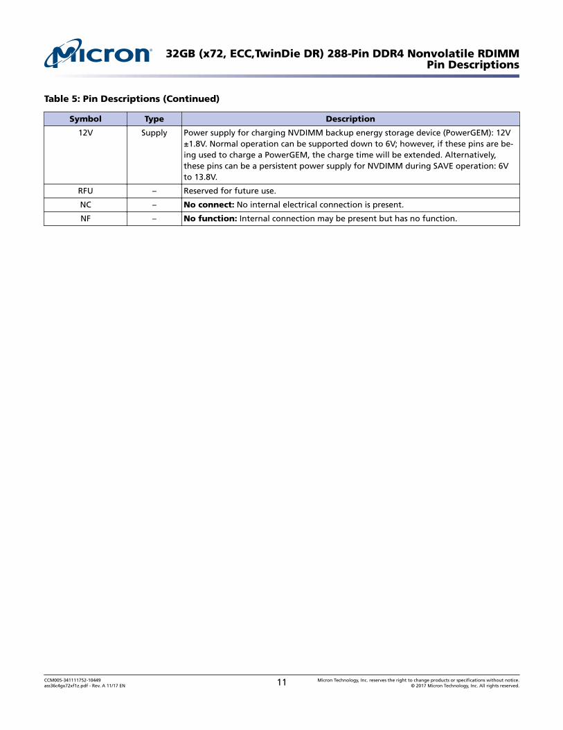
12V Supply Power supply for charging NVDIMM backup energy storage device (PowerGEM): 12V±1.8V. Normal operation can be supported down to 6V; however, if these pins are be-ing used to charge a PowerGEM, the charge time will be extended. Alternatively,these pins can be a persistent power supply for NVDIMM during SAVE operation: 6Vto 13.8V.
RFU – Reserved for future use.
NC – No connect: No internal electrical connection is present.
NF – No function: Internal connection may be present but has no function.
CCM005-341111752-10449ass36c4gx72xf1z.pdf - Rev. A 11/17 EN 11 Micron Technology, Inc. reserves the right to change products or specifications without notice.
CCM005-341111752-10449ass36c4gx72xf1z.pdf - Rev. A 11/17 EN 12 Micron Technology, Inc. reserves the right to change products or specifications without notice.
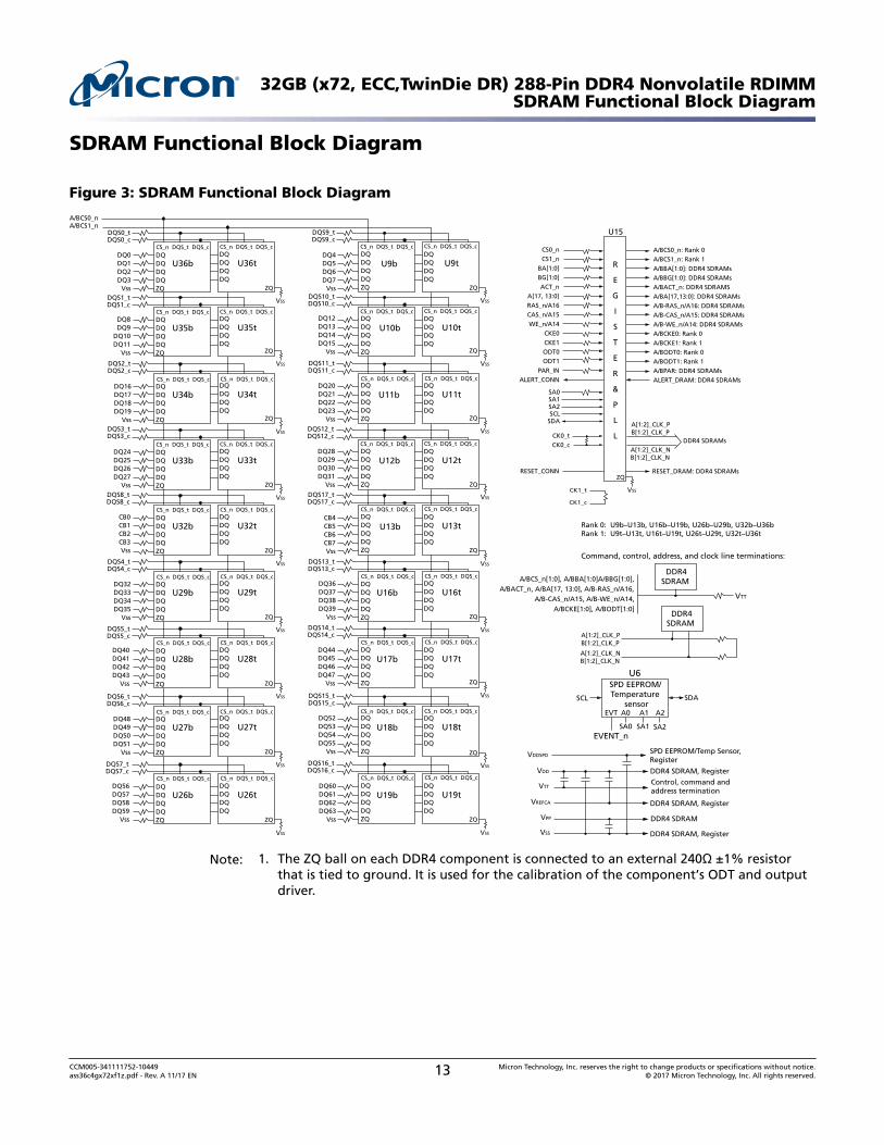
Note: 1. The ZQ ball on each DDR4 component is connected to an external 240Ω ±1% resistorthat is tied to ground. It is used for the calibration of the component’s ODT and outputdriver.
CCM005-341111752-10449ass36c4gx72xf1z.pdf - Rev. A 11/17 EN 13 Micron Technology, Inc. reserves the right to change products or specifications without notice.
Micron NVDIMM General DescriptionMicron NVDIMM is a new class of nonvolatile memory developed to meet the need forhigher-density, higher-performance memory for enterprise-class storage and server ap-plications. By combining DRAM, flash, an intelligent system controller, and an ultraca-pacitor power source, Micron NVDIMM provides a highly reliable memory subsystemthat runs with the latency and endurance of the fastest DRAM, and with the persistenceof flash. Until recently, designers have reluctantly used batteries to maintain their dataduring power outages. Others have moved toward new flash-based technologies formemory persistence, but this option falls short of DRAM in terms of latency, speed, en-durance, and reliability. Micron NVDIMM enables the fastest possible system perform-ance while eliminating the many problems associated with batteries, such as hazardousmaterial disposal, short operating life, and extensive maintenance.
The Micron DDR4 NVDIMM has been specifically designed to operate with host sys-tems that have implemented the asynchronous DRAM refresh (ADR) feature, althoughit is possible to integrate into systems that do not have this enabled. Please contact Mi-cron for more details on system integration requirements and instructions.
During normal operation, bypass mode, the Micron DDR4 NVDIMM appears as astandard registered DDR4 DIMM to the host system, providing all the benefits andspeed of a high-speed, high-density SDRAM. In the event of a power loss, the MicronNVDIMM controller can be commanded to take control of the SDRAM, transferring itscontents to flash memory using energy from its own battery-free power source or from asystem-level persistent power source, thereby preserving all of the SDRAM data. Afterpower is restored, the Micron NVDIMM controller can be commanded to transfer thecontents from the flash back to the SDRAM and return control to the host system.
DDR4 RDIMM Functionality
DDR4 SDRAM modules are high-speed, CMOS dynamic random access memory mod-ules that use internally configured 16-bank DDR4 SDRAM devices. DDR4 SDRAM mod-ules use DDR architecture to achieve high-speed operation. DDR4 is essentially an 8n-prefetch architecture with an interface designed to transfer two data words per clock cy-cle at the I/O pins. A single read or write access for the DDR4 SDRAM module effectivelyconsists of a single 8n-bit-wide, one-clock-cycle data transfer at the internal DRAM coreand eight corresponding n-bit-wide, one-half-clock-cycle data transfers at the I/O pins.
DDR4 modules use two sets of differential signals: DQS_t/DQS_c to capture data andCK_t/CK_c to capture commands, addresses, and control signals. Differential clocksand data strobes ensure exceptional noise immunity for these signals and provide pre-cise crossing points to capture input signals.
Fly-By Topology
DDR4 modules, such as this NVDIMM, use faster clock speeds than earlier DDR tech-nologies, making signal quality more important than ever. For improved signal quality,the clock, control, command, and address buses have been routed in a fly-by topology,where each clock, control, command, and address pin on each DRAM is connected to asingle trace and terminated (rather than a tree structure, where the termination is offthe module near the connector). Inherent to fly-by topology, the timing skew betweenthe clock and DQS signals can be easily accounted for by using the write-leveling fea-ture of DDR4.
CCM005-341111752-10449ass36c4gx72xf1z.pdf - Rev. A 11/17 EN 14 Micron Technology, Inc. reserves the right to change products or specifications without notice.
Registering Clock Driver OperationRegistered DDR4 SDRAM modules use a registering clock driver device consisting of aregister and a phase-lock loop (PLL). The device complies with the JEDEC DDR4 RCDspecification.
To reduce the electrical load on the host memory controller's command, address, andcontrol bus, Micron's RDIMMs utilize a DDR4 registering clock driver (RCD). The RCDpresents a single load to the controller while redriving signals to the DDR4 SDRAM de-vices, which helps enable higher densities and increase signal integrity. The RCD alsoprovides a low-jitter, low-skew PLL that redistributes a differential clock pair to multipledifferential pairs of clock outputs.
Control Words
The RCD device(s) used on DDR4 RDIMMs, LRDIMMs, and NVDIMMs contain configu-ration registers known as control words, which the host uses to configure the RCDbased on criteria determined by the module design. Control words can be set by thehost controller through either the DRAM address and control bus or the I2C bus inter-face. The RCD I2C bus interface resides on the same I2C bus interface as the moduletemperature sensor and EEPROM.
Parity Operations
The RCD includes a parity-checking function that can be enabled or disabled in controlword RC0E. The RCD receives a parity bit at the DPAR input from the memory control-ler and compares it with the data received on the qualified command and address in-puts; it indicates on its open-drain ALERT_n pin whether a parity error has occurred. Ifparity checking is enabled, the RCD forwards commands to the SDRAM when no parityerror has occurred. If the parity error function is disabled, the RCD forwards sampledcommands to the SDRAM regardless of whether a parity error has occurred. Parity is al-so checked during control word WRITE operations unless parity checking is disabled.
Rank Addressing
The chip select pins (CS_n) on Micron's modules are used to select a specific rank ofDRAM. The RDIMM is capable of selecting ranks in one of three different operatingmodes, dependant on setting DA[1:0] bits in the DIMM configuration control word lo-cated within the RCD. Direct DualCS mode is utilized for single- or dual-rank modules.For quad-rank modules, either direct or encoded QuadCS mode is used.
CCM005-341111752-10449ass36c4gx72xf1z.pdf - Rev. A 11/17 EN 15 Micron Technology, Inc. reserves the right to change products or specifications without notice.
Temperature Sensor with Serial Presence-Detect EEPROM
Thermal Sensor Operations
The integrated thermal sensor continuously monitors the temperature of the DIMMPCB directly below the device and updates the temperature data register. Temperaturedata may be read from the bus host at any time providing the host real time feedback ofmodule temperature. Thermal senors will provide a temperature resolution of 0.5, 0.25,0.125, or 0.0625 °C. It is recommended that the system read the Temperature Sensor Ca-pabilities register during system initialization to determine the temperature resolutionutilized. System designers may utilize the multiple programmable and read-only tem-perature registers to create a custom temperature sensing solution based on system re-quirements and JEDEC JC-42.2.
EVENT_n Pin
The temperature sensor also adds the EVENT_n pin. This is an open-drain output thatrequires a pull-up to VDDSPD. Not used by the SPD EEPROM, EVENT_n is a temperaturesensor output used to flag critical events that can be set up in the sensor’s configurationregisters. The Micron NVDIMM controller can also be configured to drive EVENT_nLOW to indicate that "good-to-go" status is LOW and that the Micron NVDIMM may nolonger be nonvolatile. See the NVDIMM firmware document for details on how this isconfigured.
• EVENT_n has three defined modes of operation: interrupt mode, comparator mode,and TCRIT only.
• In interrupt mode the EVENT_n pin will remain asserted until it is released by writinga 1 to the clear event bit in the status register.
• In comparator mode the EVENT_n pin will clear itself when the error condition is re-moved. This mode is always used when the temperature is compared against theTCRIT limit.
• In TCRIT only mode the EVENT_n pin will only be asserted if the measured tempera-ture exceeds the TCRIT limit. It will remain asserted until the temperature drops be-low the TCRIT limits minus the TCRIT hysteresis.
Serial Presence-Detect EEPROM Operation
DDR4 SDRAM modules incorporate serial presence-detect. The SPD data is stored in a512-byte JEDEC JC-42.4 compliant EEPROM that is segregated into 4, 128-byte, writeprotectable blocks. The SPD content is aligned with these blocks as follows.
Block Range Description
0 0–127 0x000–0x07F Configuration and DRAM parameters
1 128–255 0x080–0x0FF Module parameters
2 256–319 0x100–0x13F Reserved – All bytes coded as 0x00
320–383 0x140–0x17F Manufacturing information
3 384–511 0x180–0x1FF End user programmable
The first 384 bytes are programmed by Micron, the remaining 128 bytes of storage areavailable for use by the customer.
32GB (x72, ECC,TwinDie DR) 288-Pin DDR4 Nonvolatile RDIMMTemperature Sensor with Serial Presence-Detect EEPROM
CCM005-341111752-10449ass36c4gx72xf1z.pdf - Rev. A 11/17 EN 16 Micron Technology, Inc. reserves the right to change products or specifications without notice.
The EEPROM resides on a two-wire I2C serial interface and is not integrated with thememory bus in any manner. It operates as a slave device in the I2C bus protocol, with alloperations synchronized by the serial clock. Transfer rates of up to 1 MHz are achieva-ble at 2.2–3.6V.
Micron implements reversible software write protection on DDR4 SDRAM-based mod-ules. This prevents the lower 384 bytes (bytes 0–383) from being inadvertently program-med or corrupted. The upper 128 bytes remain available for customer use and unpro-tected.
I2C Address Map
Micron NVDIMMs have multiple devices connected to the system I2C-compatibleSMBus. The system accessible address spaces for these devices are provided below forreference as these devices may have content or configurable registers that can be ac-cessed by the system. All applicable specifications must be followed when accessingthese address spaces to ensure proper operation of the NVDIMM.
I2C Address Map
NVDIMM controller 0x10–0x17
Temperature sensor 0x18–0x1F
SPD EEPROM – PAGE/WRITE PROTECT 0x30–0x37
SPD EEPROM – READ/WRITE 0x50–0x57
Registering clock drive (RCD) 0x58–0x5F
Notes: 1. SA[2:0] must be set accordingly to address a device on a specific module.2. SPD EEPROM: PAGE and WRITE PROTECT do not use SA[2:0]. These commands are
broadcast to SPD EEPROMs on all the modules in the bus.
32GB (x72, ECC,TwinDie DR) 288-Pin DDR4 Nonvolatile RDIMMTemperature Sensor with Serial Presence-Detect EEPROM
CCM005-341111752-10449ass36c4gx72xf1z.pdf - Rev. A 11/17 EN 17 Micron Technology, Inc. reserves the right to change products or specifications without notice.
Micron NVDIMM controller copying DRAM contentsto NAND Flash
tSAVE 32GB TBD TBD sec 3
Micron NVDIMM controller copying an image fromNAND Flash to DRAM
tRESTORE 32GB TBD TBD sec 4
NAND is available for a SAVE after a ERASE com-mand is issued
tERASE – TBD sec
CSAVE trigger to switched MUX. Host must continueto maintain VDD, keep SDRAM in self refresh, andnot assert DDR4 RESET_n to avoid data loss
tMUX_SWITCH TBD TBD μs
Notes: 1. Max time will be reached when the NVDIMM is reset following a firmware update.2. All conditions defined in the NVDIMM firmware specification must be met for the
NVDIMM_RDY register to be set indicating to the host that the NVDIMM can be used asnonvolatile memory. tES_CHRG MAX is defined as the charge time of the ultracapacitorsfrom a completely discharged state. Values shown in this table reflect times observedwith a typical PowerGEM configuration for the given NVDIMM density. The actual maxi-mum time will depend on the specific PowerGEM used. See the PowerGEM data sheetfor details.
3. If the NVDIMM encounters errors during the SAVE, it will continue to attempt to saveuntil it either runs out of power or a command is sent to the NVDIMM to cancel theSAVE operation.
4. Maximum restore time based on 10,000 ECC correction limit on the NAND Flash.
CCM005-341111752-10449ass36c4gx72xf1z.pdf - Rev. A 11/17 EN 18 Micron Technology, Inc. reserves the right to change products or specifications without notice.
Electrical SpecificationsStresses greater than those listed may cause permanent damage to the module. This is astress rating only, and functional operation of the module at these or any other condi-tions outside those indicated in each device's data sheet is not implied. Exposure to ab-solute maximum rating conditions for extended periods may adversely affect reliability.
Table 8: Absolute Maximum Ratings
Symbol Parameter Min Max Units Notes
VDD VDD supply voltage relative to VSS –0.4 1.5 V 1
VDDQ VDDQ supply voltage relative to VSS –0.4 1.5 V 1
VPP Voltage on VPP pin relative to VSS –0.4 3.0 V 2
12V Voltage on 12V pin relative to VSS –0.4 13.8 V
VIN, VOUT Voltage on any pin relative to VSS –0.4 1.5 V
Notes: 1. VDDQ balls on DRAM are tied to VDD.2. VPP must be greater than or equal to VDD at all times.
Table 9: Operating Conditions
Symbol Parameter Min Nom Max Units Notes
VDD VDD supply voltage 1.14 1.2 1.26 V 1
VPP DRAM activating power supply 2.375 2.5 2.750 V 2
12V Auxiliary NVDIMM power supply 6 12 13.8 V
VREFCA(DC) Input reference voltage command/address bus 0.49 × VDD 0.5 × VDD 0.51 × VDD V 3
VTT Termination reference voltage (DC) – command/address bus
= VDD/2 (All other pins not under test = 0V)–2 0 +2 µA 7
Notes: 1. VDDQ balls on DRAM are tied to VDD.2. VPP must be greater than or equal to VDD at all times.3. VREFCA must not be greater than 0.6 x VDD. When VDD is less than 500mV, VREF may be
less than or equal to 300mV.4. VTT termination voltages in excess of specification limit will adversely affect command
and address signals' voltage margins, and reduce timing margins.
CCM005-341111752-10449ass36c4gx72xf1z.pdf - Rev. A 11/17 EN 19 Micron Technology, Inc. reserves the right to change products or specifications without notice.
5. Command and address inputs are terminated to VDD/2 in the registering clock driver. In-put current is dependent on terminating resistance selected in registering clock driver.
6. Tied to ground. Not connected to edge connector.7. Multiply by number of DRAM die on module.
Table 10: Thermal Characteristics
The NVDIMM consists of many devices with differing temperature specifications. It is the responsibility of the system de-signer to ensure the temperature specifications are maintained for all devices.Device Parameter/Condition Temp Units Notes
DRAM DRAM case temperature - Measured at the center top of die.The DRAM consumes power in all modes as per IDD tables in Mi-cron DDR4 component data sheets. The memory bus operates ata lower frequency during backup and restore operations there-fore dissipating less power then when operating in bypassmode.
TCASE 0 to 85°C 1, 2, 3
TCASE >85 to95°C
1, 2, 3, 4
TJUNCTION 0 to100°C
ΘJC 4.2°C/Watt
NAND Flash NF is utilized during backup and restore operations. The NF isnot utilized during bypass mode therefore making temperaturespecifications relatively simple to maintain.
TCASE 0 to 80°C 1, 2, 3
TJUNCTION 0 to 85°C
ΘJC 0.7°C/Watt
FPGA (NV Con-troller)
Powered during bypass mode and only fully utilized during a re-store or backup operation. DRAM bus is operated at a lowerclock frequency during backup and restore operations.
TCASE Not speci-fied
1, 2, 3
TJUNCTION TBD
ΘJC TBD
PSOC (NV Con-troller)
Powered during bypass mode and only fully utilized during a re-store or backup operation. DRAM bus is operated at a lowerclock frequency during backup and restore operations.
TCASE Not speci-fied
1, 2, 3
TJUNCTION TBD
ΘJC TBD
NOR Holds the code and fabric for the NV controller. Utilized duringinitialization.
TCASE Not speci-fied
1, 2, 3
TJUNCTION 0 to 90°C
ΘJC 5°C/Watt
RCD Resides on Command/Address bus and consumes power in allmodes. DRAM bus is operated at a lower frequency during back-up and restore operations, therefore consuming less power.
TCASE 0 to 103°C 1, 2, 3
TJUNCTION 0 to 125°C
Notes: 1. Maximum operating case temperature. TC is measured in the center of the device pack-age.
2. A thermal solution must be designed to ensure the device does not exceed the maxi-mum temperature during operation.
3. Device functionality is not guaranteed if the device exceeds the maximum temperatureduring operation.
4. If TC exceeds 85°C, the DRAM device must be refreshed externally at 2X refresh (a 3.9µsinterval refresh rate).
CCM005-341111752-10449ass36c4gx72xf1z.pdf - Rev. A 11/17 EN 20 Micron Technology, Inc. reserves the right to change products or specifications without notice.
When a CSAVE or a RESTORE operation is in progress.
Slow Blink(every 15 seconds)
Normal operation: Controller fabric and FW has been loaded. NVDIMM is op-erational from host perspective.
D3 AmberUser Defined
ON/OFF The state of this LED is user configurable. The host may write 0x01 to the LEDregister (0x10) to turn the amber LED ON, and 0x00 to turn the amber LEDoff. Reading this register returns the state of the output register, not the buf-fered LED driver output.
Any Any undefined NVDIMM hardware or firmware failure
I/O This open drain signal is used by the NVRDIMM to force the Power-GEM to begin discharging by driving LOW. A low voltage level detec-ted by the NV controller on this pin indicates the PowerGEM is con-nected. A high voltage level indicates the PowerGEM is not connec-ted.
4 Power_Fail_Int# Input Active LOW signal indicates input power is below defined threshold.Can be used as an alternative trigger for CSAVE. See PowerGEM datasheet.
5 VSS Supply Ground.
6 12C/VDD_cap Supply 12V supply to PowerGEM from host. 12V supply from PowerGEM toNVRDIMM when 12V rail is removed at host.
CCM005-341111752-10449ass36c4gx72xf1z.pdf - Rev. A 11/17 EN 21 Micron Technology, Inc. reserves the right to change products or specifications without notice.
DRAM Operating ConditionsRecommended AC operating conditions are given in the DDR4 component data sheets.Component specifications are available at micron.com. Module speed grades correlatewith component speed grades, as shown below.
Table 13: Module and Component Speed Grades
DDR4 components may exceed the listed module speed grades; module may not be available in all listed speed gradesModule Speed Grade Component Speed Grade
-3G2 -062E
-2G9 -068
-2G6 -075
-2G3 -083
-2G1 -093E
Design Considerations
Simulations
Micron memory modules are designed to optimize signal integrity through carefully de-signed terminations, controlled board impedances, routing topologies, trace lengthmatching, and decoupling. However, good signal integrity starts at the system level. Mi-cron encourages designers to simulate the signal characteristics of the system's memo-ry bus to ensure adequate signal integrity of the entire memory system.
Power
Operating voltages are specified at the edge connector of the module, not at the DRAM.Designers must account for any system voltage drops at anticipated power levels to en-sure the required supply voltage is maintained.
CCM005-341111752-10449ass36c4gx72xf1z.pdf - Rev. A 11/17 EN 22 Micron Technology, Inc. reserves the right to change products or specifications without notice.
Values are for the MT40A4G4 DDR4 TwinDie SDRAM only and are computed from values specified in the 16Gb (4 Gig x 4)component data sheetParameter Symbol 2933 2666 2400 Units
One bank ACTIVATE-PRECHARGE current ICDD0 1386 1332 1278 mA
One bank ACTIVATE-PRECHARGE, wordline boost, IPP current ICPP0 108 108 180 mA
One bank ACTIVATE-READ-PRECHARGE current ICDD1 1602 1548 1494 mA
Precharge standby current ICDD2N 1098 1080 1062 mA
Precharge standby ODT current ICDD2NT 1440 1350 1350 mA
Precharge power-down current ICDD2P 900 900 900 mA
Precharge quite standby current ICDD2Q 990 990 990 mA
Active standby current ICDD3N 1332 1278 1224 mA
Active standby IPP current ICPP3N 108 108 108 mA
Active power-down current ICDD3P 1098 1062 1026 mA
Burst read current ICDD4R 2880 2682 2484 mA
Burst write current ICDD4W 2844 2700 2538 mA
Burst refresh current (1x REF) ICDD5R 1602 1548 1494 mA
Burst refresh IPP current (1x REF) ICPP5R 144 144 144 mA
Self refresh current: Normal temperature range (0°C to 85°C) ICDD6N 1116 1116 1116 mA
Self refresh current: Extended temperature range (0°C to 95°C) ICDD6E 1296 1296 1296 mA
Self refresh current: Reduced temperature range (0°C to 45°C) ICDD6R 756 756 756 mA
Auto self refresh current (25°C) ICDD6A 309.6 309.6 309.6 mA
Auto self refresh current (45°C) ICDD6A 756 756 756 mA
Auto self refresh current (75°C) ICDD6A 1116 1116 1116 mA
Auto self refresh IPP current ICPP6X 180 180 180 mA
Bank interleave read current ICDD7 4374 4104 3834 mA
Bank interleave read IPP current ICPP7 396 378 360 mA
CCM005-341111752-10449ass36c4gx72xf1z.pdf - Rev. A 11/17 EN 23 Micron Technology, Inc. reserves the right to change products or specifications without notice.
2.5V - VDDSPD supplied from edge connector 2.5V - regulated from 12V backup supply
RCD (registeringclock driver)
1.2V - VDD supplied from edge connector 1.2V - regulated from 12V backup supply
Integrated datamuxes
2.5V - VPP supplied from edge connector 2.5V - regulated from 12V backup supply
SPD EEPROM/TS 2.5V - VDDSPD supplied from edge connector Not energized
VPD EEPROM 2.5V - VDDSPD supplied from edge connector 2.5V - regulated from 12V backup supply
32GB (x72, ECC,TwinDie DR) 288-Pin DDR4 Nonvolatile RDIMMPower Distribution
CCM005-341111752-10449ass36c4gx72xf1z.pdf - Rev. A 11/17 EN 24 Micron Technology, Inc. reserves the right to change products or specifications without notice.
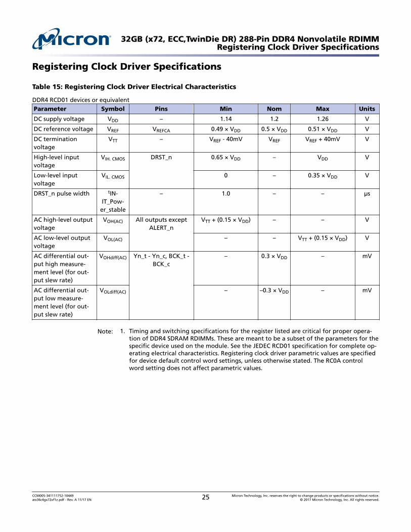
DDR4 RCD01 devices or equivalentParameter Symbol Pins Min Nom Max Units
DC supply voltage VDD – 1.14 1.2 1.26 V
DC reference voltage VREF VREFCA 0.49 × VDD 0.5 × VDD 0.51 × VDD V
DC terminationvoltage
VTT – VREF - 40mV VREF VREF + 40mV V
High-level inputvoltage
VIH. CMOS DRST_n 0.65 × VDD – VDD V
Low-level inputvoltage
VIL. CMOS 0 – 0.35 × VDD V
DRST_n pulse width tIN-IT_Pow-
er_stable
– 1.0 – – µs
AC high-level outputvoltage
VOH(AC) All outputs exceptALERT_n
VTT + (0.15 × VDD) – – V
AC low-level outputvoltage
VOL(AC) – – VTT + (0.15 × VDD) V
AC differential out-put high measure-ment level (for out-put slew rate)
VOHdiff(AC) Yn_t - Yn_c, BCK_t -BCK_c
– 0.3 × VDD – mV
AC differential out-put low measure-ment level (for out-put slew rate)
VOLdiff(AC) – –0.3 × VDD – mV
Note: 1. Timing and switching specifications for the register listed are critical for proper opera-tion of DDR4 SDRAM RDIMMs. These are meant to be a subset of the parameters for thespecific device used on the module. See the JEDEC RCD01 specification for complete op-erating electrical characteristics. Registering clock driver parametric values are specifiedfor device default control word settings, unless otherwise stated. The RC0A controlword setting does not affect parametric values.
CCM005-341111752-10449ass36c4gx72xf1z.pdf - Rev. A 11/17 EN 25 Micron Technology, Inc. reserves the right to change products or specifications without notice.
Notes: 1. All dimensions are in millimeters (inches); MAX/MIN or typical (TYP) where noted.2. The dimensional diagram is for reference only.3. Weight of module is approximately 25 grams.
8000 S. Federal Way, P.O. Box 6, Boise, ID 83707-0006, Tel: 208-368-4000www.micron.com/products/support Sales inquiries: 800-932-4992
Micron and the Micron logo are trademarks of Micron Technology, Inc.All other trademarks are the property of their respective owners.
This data sheet contains minimum and maximum limits specified over the power supply and temperature range set forth herein.Although considered final, these specifications are subject to change, as further product development and data characterization some-
CCM005-341111752-10449ass36c4gx72xf1z.pdf - Rev. A 11/17 EN 26 Micron Technology, Inc. reserves the right to change products or specifications without notice.