Copyright copy 2011 American Scientific PublishersAll rights reservedPrinted in the United States of America
Journal ofNanoscience and Nanotechnology
Vol 11 239ndash242 2011
Deformation Characteristics of an OrganicThin Film Transistor
D-K Lee1 S-C Lee1 Y-G Seol2 J-H Ahn3 N-E Lee3 and Y-J Kim4lowast1Graduate School of Mechanical Engineering Sungkyunkwan University
2Graduate School of Advanced Materials Science and Engineering Sungkyunkwan University3School of Advanced Materials Science and Engineering Sungkyunkwan University
4School of Mechanical Engineering Sungkyunkwan University 300 Cheoncheon-dong Suwon 440-746 Korea
An organic thin film transistor (OTFT) on a flexible substrate with electroplated electrodes has manyadvantages in the fabrication of low cost sensors e-paper smart cards and flexible displays Inthis study we simulated the mechanical characteristics of an OTFT with various compressive stressconditions using COMSOL An analysis model which was limited to channel source and drain wasused to investigate deformation and internal stress concentrations The channel length is 40 mand the OTFT structure is a top-contact structure The OTFT was fabricated using pentacene as asemiconducting layer and electroplated Ni as a gate electrode The deformation characteristics ofthe fabricated OTFT were predicted in terms of strain and internal stress
Keywords OTFT Neutral Mechanical Plane Radius of Curvature
1 INTRODUCTION
Organic thin film transistors (OTFTs) are of increas-ing interest in a wide range of applications due totheir unique properties Applications include flexible elec-tronic systems such as radio-frequency identification tagslow-temperature and low-cost fabrication processes lightweight mechanical flexibility low-cost sensors and flex-ible displays1ndash3 Using an OTFT is essential in achievinggood mechanical flexibility in each layer with no crackingand excellent adhesion between the layers without delam-ination during current flow Thus it is important to under-stand the mechanical characteristics of the OTFT devicelayer for effective implementation of flexible electronicsystems Until recently experimental methods have beenused to analyze the physical characteristics of thin filmYanakai et al4 studied cracking phenomena in a brittlefilm nanostructure due to bending forces Seol et al5 stud-ied improvements in the mechanical and electrical stabilityof OTFTs using an adhesive organic interlayer Howeverthere are few studies of the bending of OTFTWe developed an analysis method for OTFT compared
results from numerical analysis with experimental resultsand interpreted the physical characteristics of compressivestress conditions
lowastAuthor to whom correspondence should be addressed
2 THEORY
The governing equation relating stress and strain is6
= E (1)
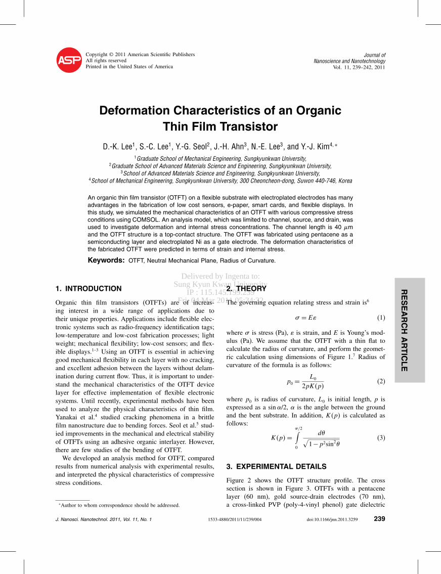
where is stress (Pa) is strain and E is Youngrsquos mod-ulus (Pa) We assume that the OTFT with a thin flat tocalculate the radius of curvature and perform the geomet-ric calculation using dimensions of Figure 17 Radius ofcurvature of the formula is as follows
p0 =L0
2pKp(2)
where p0 is radius of curvature L0 is initial length p isexpressed as a sin2 is the angle between the groundand the bent substrate In addition Kp is calculated asfollows
Kp=2int
0
dradic1minusp2sin2
(3)
3 EXPERIMENTAL DETAILS
Figure 2 shows the OTFT structure profile The crosssection is shown in Figure 3 OTFTs with a pentacenelayer (60 nm) gold source-drain electrodes (70 nm)a cross-linked PVP (poly-4-vinyl phenol) gate dielectric
Deformation Characteristics of an Organic Thin Film Transistor Lee et al
Fig 1 The diagram of radius of curvature
layer (400 nm) and electroplated Ni gate electrodes(150 nm) were fabricated on 125 m PI film (Du PontKaptonreg) We made the OTFT (5 cm) the same way asdescribed in Ref [4] As shown in Figure 4 we com-pressed the B side until the interval d was 15 cm thenthe A side is pinned We ignored initial state (deformationtwist stress and strain) to analyze the mechanical charac-teristics of the OTFT We have taken pictures of the sideof channel and measured and to obtain the radius ofcurvature
4 NUMERICAL ANALYSIS
Numerical simulation of elastic deformation was con-ducted using compressive stress We considered the multi-layer structure but the cracking and fracture of inorganicmaterials were ignored In the present studies we con-sider using COMSOL Multiphysics 35a strain and internalstress
41 Model and Grid Systems
Figure 5 shows a grid for our limited analysis 3-D model8
The channel length and width are 40 m and 800 mrespectively The bonding of the inorganic and organic
Fig 2 Structure of OTFT on the polyimide
Fig 3 Schematic diagram of the channel-cross sectional area
Fig 4 Equipment for bending experiment
parts is vulnerable to bending and has the greatest impacton performance so the analysis model was limited tothe channel source gate and semiconductor layers Thedomain of all elements was composed of hybrid grid sys-tems in order to establish a discrete system for numeri-cal simulation We used nearly 100000 elements for theOTFT structure with the structural analysis setup as shownin Figure 4 The length of the x-direction was set to be103 times longer than the length of the z-direction Fora narrow region we formed at least three element layersalong the vertical direction
42 Analysis Condition
We use Eq (1) to calculate substrate deformation causedby external force As shown in Figure 5 the stress wascompressed until 400 MPa We did not consider a changein strain due to a crack or fracture It was assumedthat nickel and gold did not undergo plastic deformationbecause most of the OTFT organic and inorganic materialsare thin
Fig 5 Limited part of the element system for numerical analysis of thechannel
240 J Nanosci Nanotechnol 11 239ndash242 2011
Delivered by Ingenta toSung Kyun Kwan University
IP 115145199239Fri 04 Mar 2011 053432
RESEARCH
ARTIC
LE
Lee et al Deformation Characteristics of an Organic Thin Film Transistor
Fig 6 Result of numerical analysis in compressive stress condition
5 RESULTS AND DISCUSSION
Figure 6 shows the deformed numerical analysis modelin a 20 MPa compressed condition In the central part ofthe substrate buckling occurs due to compressive stress inthe x-axis direction Figure 7 shows the numerical analy-sis results of the change in compressive stress comparedto experimental results based on the strain and the radiusof curvature The radius of curvature of the flat substrateis infinite from the experiment results but the radius ofcurvature will converge to 0 as strain increase Numericalanalysis results are also similar to experiment results Theaverage error between experimental and numerical analy-sis results is about 00199 m in the strain range from 0 to005 and is about 000923 m in the strain range from 005to 03 Although the average error is big in the range from0 to 005 overall strain-radius trend of curvature graph issimilarThe strain direction of the x-axis is an important ele-
ment in determining the direction of the stress The neutral
00 01 02 03
00
02
04
Rad
ius
(m)
Strain
ExperimentNumerical analysis
Radius error 0ltstrainlt005 199 mm
005ltstrainlt03 92 mm
Fig 7 Similarities between experimental and numerical analysis strain-curvature curve
Fig 8 Neutral plane of OTFT structure (zero strain point)
Fig 9 Von Mises stress distribution on the device
plane defines the position where the strains are zero Wecan see the neutral plane of the OTFT in Figure 8 Theneutral plane is the point 105 m from the bottom Basedon the neutral plane the tensile stress is acting on theupper layer and the compression stress is acting on thelower layer For this reason tensile stress is working inthe electrode devices Figure 9 shows the tensile stress dis-tribution at the cross-sectional area of the channel alongthe z-direction In general tensile stress is concentratedon inorganic materials (Ni and Au) because the Youngrsquosmodulus of inorganic material is larger than that of theorganic one
6 CONCLUSIONS
In this work the mechanical properties of an OTFT withapplied compressive stress were evaluated using the results
J Nanosci Nanotechnol 11 239ndash242 2011 241
Delivered by Ingenta toSung Kyun Kwan University
IP 115145199239Fri 04 Mar 2011 053432
RESEARCH
ARTIC
LE
Deformation Characteristics of an Organic Thin Film Transistor Lee et al
of strain and internal stress The following conclusionswere drawn(1) We have established how to interpret the mechanicalOTFT by comparing the experimental results and numeri-cal analysis(2) Significantly numerical analysis error occurred after2 strain so research considering plastic deformation ofinorganic materials is necessary(3) Tensile stress on the neutral plane is caused by theexternal force Therefore the crack may occur in the inor-ganic materials (Ni and Au) It is necessary to do moreresearch with crack in the thin film
Acknowledgments Financial aid from the Korea Min-istry of Education through the Brain Korea 21 Project isgratefully acknowledged The authors are also grateful for
the financial support provided by Korea Research Founda-tion (R01-2008-000-20533-0)
References and Notes
1 S Steudel S De Vusser S De Jonge D Janssen S VerlaakJ Genoe and P Heremans Appl Phys Lett 85 4400 (2004)
2 P Mach S J Rodriguez R Nortrup P Wiltzius and J A RogersAppl Phys Lett 78 3592 (2001)
3 L A Majewski M Grell S D Ogier and J Veres Org Electron4 27 (2003)
4 M Yanaka Y Tsukahara N Nakso and N Takeda J Mater Sci33 2111 (1998)
5 Y G Seol N E Lee S H Park and J Y Bea Org Electron9 413 (2008)
6 R C Hibbeler Mech Mater 5 572 (2005)7 S P Timoshenko and J N Goodier Theory of Elasticity 3rd edn
McGraw-Hill Kogakusha Tokyo (1970)8 R W Johnstone and M Parameswaran Can J Elect Comput Eng
29 3 (2004)
Received 8 June 2009 Accepted 28 December 2009
242 J Nanosci Nanotechnol 11 239ndash242 2011
Delivered by Ingenta toSung Kyun Kwan University
IP 115145199239Fri 04 Mar 2011 053432
RESEARCH
ARTIC
LE
Deformation Characteristics of an Organic Thin Film Transistor Lee et al
Fig 1 The diagram of radius of curvature
layer (400 nm) and electroplated Ni gate electrodes(150 nm) were fabricated on 125 m PI film (Du PontKaptonreg) We made the OTFT (5 cm) the same way asdescribed in Ref [4] As shown in Figure 4 we com-pressed the B side until the interval d was 15 cm thenthe A side is pinned We ignored initial state (deformationtwist stress and strain) to analyze the mechanical charac-teristics of the OTFT We have taken pictures of the sideof channel and measured and to obtain the radius ofcurvature
4 NUMERICAL ANALYSIS
Numerical simulation of elastic deformation was con-ducted using compressive stress We considered the multi-layer structure but the cracking and fracture of inorganicmaterials were ignored In the present studies we con-sider using COMSOL Multiphysics 35a strain and internalstress
41 Model and Grid Systems
Figure 5 shows a grid for our limited analysis 3-D model8
The channel length and width are 40 m and 800 mrespectively The bonding of the inorganic and organic
Fig 2 Structure of OTFT on the polyimide
Fig 3 Schematic diagram of the channel-cross sectional area
Fig 4 Equipment for bending experiment
parts is vulnerable to bending and has the greatest impacton performance so the analysis model was limited tothe channel source gate and semiconductor layers Thedomain of all elements was composed of hybrid grid sys-tems in order to establish a discrete system for numeri-cal simulation We used nearly 100000 elements for theOTFT structure with the structural analysis setup as shownin Figure 4 The length of the x-direction was set to be103 times longer than the length of the z-direction Fora narrow region we formed at least three element layersalong the vertical direction
42 Analysis Condition
We use Eq (1) to calculate substrate deformation causedby external force As shown in Figure 5 the stress wascompressed until 400 MPa We did not consider a changein strain due to a crack or fracture It was assumedthat nickel and gold did not undergo plastic deformationbecause most of the OTFT organic and inorganic materialsare thin
Fig 5 Limited part of the element system for numerical analysis of thechannel
240 J Nanosci Nanotechnol 11 239ndash242 2011
Delivered by Ingenta toSung Kyun Kwan University
IP 115145199239Fri 04 Mar 2011 053432
RESEARCH
ARTIC
LE
Lee et al Deformation Characteristics of an Organic Thin Film Transistor
Fig 6 Result of numerical analysis in compressive stress condition
5 RESULTS AND DISCUSSION
Figure 6 shows the deformed numerical analysis modelin a 20 MPa compressed condition In the central part ofthe substrate buckling occurs due to compressive stress inthe x-axis direction Figure 7 shows the numerical analy-sis results of the change in compressive stress comparedto experimental results based on the strain and the radiusof curvature The radius of curvature of the flat substrateis infinite from the experiment results but the radius ofcurvature will converge to 0 as strain increase Numericalanalysis results are also similar to experiment results Theaverage error between experimental and numerical analy-sis results is about 00199 m in the strain range from 0 to005 and is about 000923 m in the strain range from 005to 03 Although the average error is big in the range from0 to 005 overall strain-radius trend of curvature graph issimilarThe strain direction of the x-axis is an important ele-
ment in determining the direction of the stress The neutral
00 01 02 03
00
02
04
Rad
ius
(m)
Strain
ExperimentNumerical analysis
Radius error 0ltstrainlt005 199 mm
005ltstrainlt03 92 mm
Fig 7 Similarities between experimental and numerical analysis strain-curvature curve
Fig 8 Neutral plane of OTFT structure (zero strain point)
Fig 9 Von Mises stress distribution on the device
plane defines the position where the strains are zero Wecan see the neutral plane of the OTFT in Figure 8 Theneutral plane is the point 105 m from the bottom Basedon the neutral plane the tensile stress is acting on theupper layer and the compression stress is acting on thelower layer For this reason tensile stress is working inthe electrode devices Figure 9 shows the tensile stress dis-tribution at the cross-sectional area of the channel alongthe z-direction In general tensile stress is concentratedon inorganic materials (Ni and Au) because the Youngrsquosmodulus of inorganic material is larger than that of theorganic one
6 CONCLUSIONS
In this work the mechanical properties of an OTFT withapplied compressive stress were evaluated using the results
J Nanosci Nanotechnol 11 239ndash242 2011 241
Delivered by Ingenta toSung Kyun Kwan University
IP 115145199239Fri 04 Mar 2011 053432
RESEARCH
ARTIC
LE
Deformation Characteristics of an Organic Thin Film Transistor Lee et al
of strain and internal stress The following conclusionswere drawn(1) We have established how to interpret the mechanicalOTFT by comparing the experimental results and numeri-cal analysis(2) Significantly numerical analysis error occurred after2 strain so research considering plastic deformation ofinorganic materials is necessary(3) Tensile stress on the neutral plane is caused by theexternal force Therefore the crack may occur in the inor-ganic materials (Ni and Au) It is necessary to do moreresearch with crack in the thin film
Acknowledgments Financial aid from the Korea Min-istry of Education through the Brain Korea 21 Project isgratefully acknowledged The authors are also grateful for
the financial support provided by Korea Research Founda-tion (R01-2008-000-20533-0)
References and Notes
1 S Steudel S De Vusser S De Jonge D Janssen S VerlaakJ Genoe and P Heremans Appl Phys Lett 85 4400 (2004)
2 P Mach S J Rodriguez R Nortrup P Wiltzius and J A RogersAppl Phys Lett 78 3592 (2001)
3 L A Majewski M Grell S D Ogier and J Veres Org Electron4 27 (2003)
4 M Yanaka Y Tsukahara N Nakso and N Takeda J Mater Sci33 2111 (1998)
5 Y G Seol N E Lee S H Park and J Y Bea Org Electron9 413 (2008)
6 R C Hibbeler Mech Mater 5 572 (2005)7 S P Timoshenko and J N Goodier Theory of Elasticity 3rd edn
McGraw-Hill Kogakusha Tokyo (1970)8 R W Johnstone and M Parameswaran Can J Elect Comput Eng
29 3 (2004)
Received 8 June 2009 Accepted 28 December 2009
242 J Nanosci Nanotechnol 11 239ndash242 2011
Delivered by Ingenta toSung Kyun Kwan University
IP 115145199239Fri 04 Mar 2011 053432
RESEARCH
ARTIC
LE
Deformation Characteristics of an Organic Thin Film Transistor Lee et al
of strain and internal stress The following conclusionswere drawn(1) We have established how to interpret the mechanicalOTFT by comparing the experimental results and numeri-cal analysis(2) Significantly numerical analysis error occurred after2 strain so research considering plastic deformation ofinorganic materials is necessary(3) Tensile stress on the neutral plane is caused by theexternal force Therefore the crack may occur in the inor-ganic materials (Ni and Au) It is necessary to do moreresearch with crack in the thin film
Acknowledgments Financial aid from the Korea Min-istry of Education through the Brain Korea 21 Project isgratefully acknowledged The authors are also grateful for
the financial support provided by Korea Research Founda-tion (R01-2008-000-20533-0)
References and Notes
1 S Steudel S De Vusser S De Jonge D Janssen S VerlaakJ Genoe and P Heremans Appl Phys Lett 85 4400 (2004)
2 P Mach S J Rodriguez R Nortrup P Wiltzius and J A RogersAppl Phys Lett 78 3592 (2001)
3 L A Majewski M Grell S D Ogier and J Veres Org Electron4 27 (2003)
4 M Yanaka Y Tsukahara N Nakso and N Takeda J Mater Sci33 2111 (1998)
5 Y G Seol N E Lee S H Park and J Y Bea Org Electron9 413 (2008)
6 R C Hibbeler Mech Mater 5 572 (2005)7 S P Timoshenko and J N Goodier Theory of Elasticity 3rd edn
McGraw-Hill Kogakusha Tokyo (1970)8 R W Johnstone and M Parameswaran Can J Elect Comput Eng