38
R. W. Erickson Department of Electrical, Computer, and Energy Engineering University of Colorado, Boulder

R. W. Erickson Department of Electrical, Computer, and Energy Engineering
University of Colorado, Boulder

Fundamentals of Power Electronics Chapter 6: Converter circuits66
6.3.5. Boost-derived isolated converters
• A wide variety of boost-derived isolated dc-dc converters can bederived, by inversion of source and load of buck-derived isolatedconverters:
• full-bridge and half-bridge isolated boost converters
• inverse of forward converter: the “reverse” converter
• push-pull boost-derived converter
Of these, the full-bridge and push-pull boost-derived isolatedconverters are the most popular, and are briefly discussed here.

Fundamentals of Power Electronics Chapter 6: Converter circuits67
Full-bridge transformer-isolatedboost-derived converter
• Circuit topologies are equivalent to those of nonisolated boostconverter
• With 1:1 turns ratio, inductor current i(t) and output current io(t)waveforms are identical to nonisolated boost converter
C R
+
v
–
L
D1
D2
1 : n
: n
i(t)
+
vT(t)
–
+–Vg
Q1
Q2
Q3
Q4
+ vL(t) –
io(t)
Fundamentals of Power Electronics Chapter 6: Converter circuits68
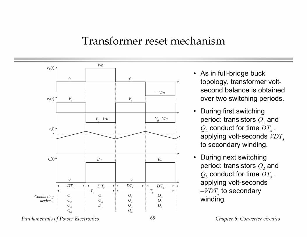
Transformer reset mechanism
• As in full-bridge bucktopology, transformer volt-second balance is obtainedover two switching periods.
• During first switchingperiod: transistors Q1 andQ4 conduct for time DTs ,applying volt-seconds VDTsto secondary winding.
• During next switchingperiod: transistors Q2 andQ3 conduct for time DTs ,applying volt-seconds–VDTs to secondarywinding.
vL(t)
i(t)
io(t)
t
Vg
0
Q1
D1
Conductingdevices:
Vg –V/n
I/n
vT(t)
0 0
V/n
– V/n
Vg
Vg –V/n
I/n
0
DTs D'TsTs
DTs D'TsTs
Q2Q3Q4
Q1Q2Q3Q4
Q1Q4
Q2Q3D2
I

Fundamentals of Power Electronics Chapter 6: Converter circuits69
Conversion ratio M(D)
Application of volt-secondbalance to inductor voltagewaveform:
Solve for M(D):
—boost with turns ratio n
vL(t)
i(t)
Vg
Vg –V/n
Vg
Vg –V/n
I
t
Q1
D1
Conductingdevices:
DTs D'TsTs
DTs D'TsTs
Q2Q3Q4
Q1Q2Q3Q4
Q1Q4
Q2Q3D2
vL = D Vg + D' Vg – Vn = 0
M(D) = VVg
= nD'

Fundamentals of Power Electronics Chapter 6: Converter circuits70
Push-pull boost-derived converter
M(D) = VVg
= nD'
+–
Vg
C R
+
V
–
L
D1
D2
1 : n
Q1
Q2
+ vL(t) –
–vT(t)
+
–vT(t)
+
io(t)
i(t)

Fundamentals of Power Electronics Chapter 6: Converter circuits71
Push-pull converter based on Watkins-Johnson converter
+–
Vg
C R
+
V
–
D1
D2
1 : n
Q1
Q2

Fundamentals of Power Electronics Chapter 6: Converter circuits72
6.3.6. Isolated versions of the SEPIC and Cuk converter
Basic nonisolatedSEPIC
Isolated SEPIC
+–
D1L1
C2
+
v
–
Q1
C1
L2RVg
+–
D1L1
C2
+
v
–
Q1
C1
RVg
1 : n
ip isi1
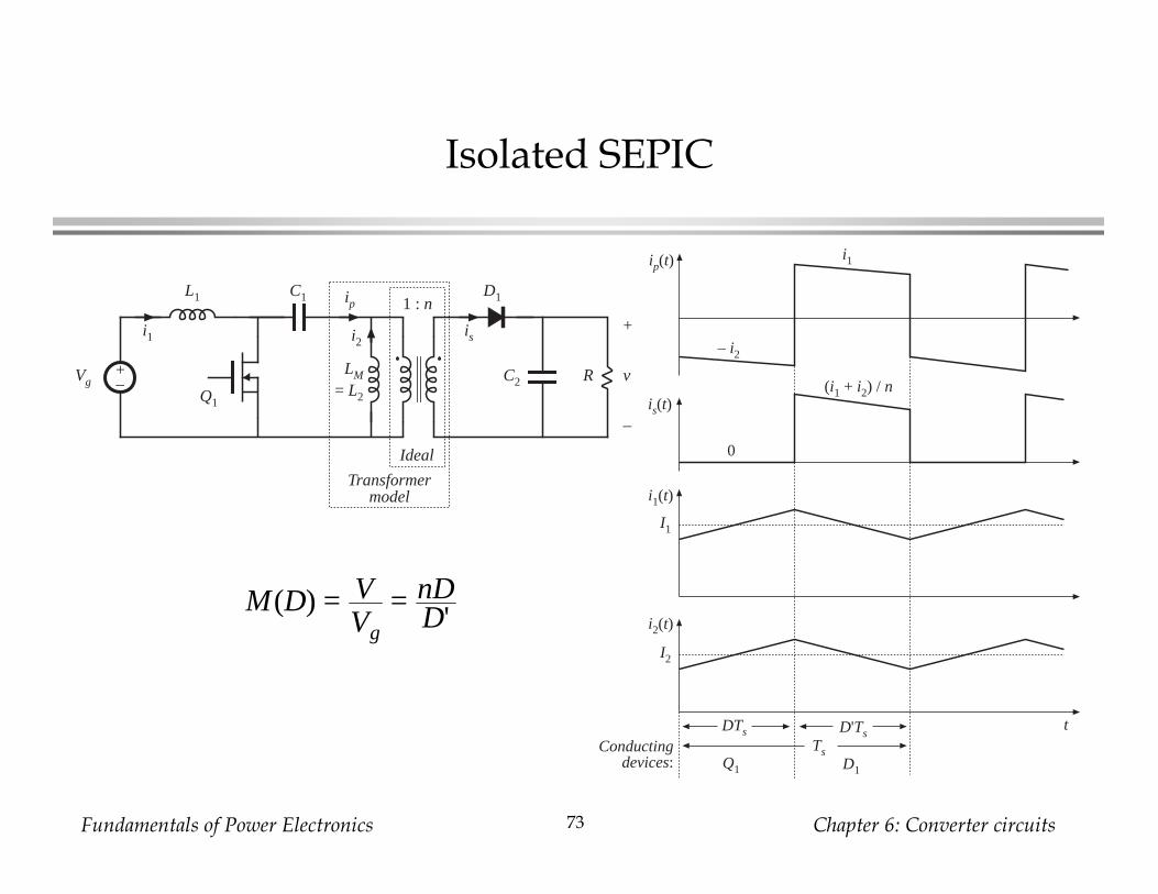
Fundamentals of Power Electronics Chapter 6: Converter circuits73
Isolated SEPIC
+–
D1L1
C2
+
v
–
Q1
C1
RVg
1 : nip
isi1 i2
Ideal
Transformermodel
LM
= L2
M(D) = VVg
= nDD'
is(t)
i1(t)
i2(t)
t
Q1 D1
Conductingdevices:
ip(t)
DTs D'TsTs
– i2
i1
0
(i1 + i2) / n
I1
I2

Fundamentals of Power Electronics Chapter 6: Converter circuits74
Inverse SEPIC
Isolated inverseSEPIC
Nonisolated inverseSEPIC
+–
D1
L2
C2
+
v
–Q1
C1
RVg
1 : n
+–
1
2Vg
+
V
–
Fundamentals of Power Electronics Chapter 6: Converter circuits75
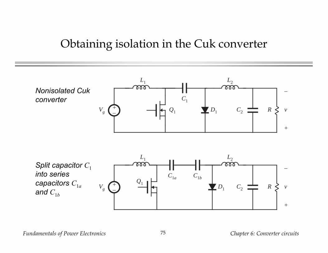
Obtaining isolation in the Cuk converter
Nonisolated Cukconverter
Split capacitor C1into seriescapacitors C1aand C1b
+– D1
L1
C2 R
–
v
+
Q1
C1
L2
Vg
+– D1
L1
C2 R
–
v
+
Q1
C1a
L2
Vg
C1b

Fundamentals of Power Electronics Chapter 6: Converter circuits76
Isolated Cuk converter
Insert transformerbetween capacitorsC1a and C1b
Discussion
• Capacitors C1a and C1b ensure that no dc voltage is applied to transformerprimary or secondary windings
• Transformer functions in conventional manner, with small magnetizingcurrent and negligible energy storage within the magnetizing inductance
+– D1
L1
C2 R
+
v
–
Q1
C1a
L2
Vg
C1b
1 : nM(D) = V
Vg
= nDD'

Fundamentals of Power Electronics Chapter 6: Converter circuits77
6.4. Converter evaluation and design
For a given application, which converter topology is best?
There is no ultimate converter, perfectly suited for all possibleapplications
Trade studies
• Rough designs of several converter topologies to meet thegiven specifications
• An unbiased quantitative comparison of worst-case transistorcurrents and voltages, transformer size, etc.
Comparison via switch stress, switch utilization, and semiconductorcost
Spreadsheet design
Fundamentals of Power Electronics Chapter 6: Converter circuits88
6.4.2. Converter design using computer spreadsheet
Given ranges of Vg and Pload , as well as desired value of V and otherquantities such as switching frequency, ripple, etc., there are twobasic engineering design tasks:
• Compare converter topologies and select the best for the givenspecifications
• Optimize the design of a given converter
A computer spreadsheet is a very useful tool for this job. The resultsof the steady-state converter analyses of Chapters 1-6 can beentered, and detailed design investigations can be quickly performed:
• Evaluation of worst-case stresses over a range of operatingpoints
• Evaluation of design tradeoffs

Fundamentals of Power Electronics Chapter 6: Converter circuits89
Spreadsheet design example
• Input voltage: rectified 230 Vrms±20%
• Regulated output of 15 V
• Rated load power 200 W
• Must operate at 10% load
• Select switching frequency of100 kHz
• Output voltage ripple ≤ 0.1V
Compare single-transistor forward and flyback converters in this application
Specifications are entered at top of spreadsheet
SpecificationsMaximum input voltage Vg 390 VMinimum input voltage Vg 260 VOutput voltage V 15 VMaximum load power Pload 200 WMinimum load power Pload 20 WSwitching frequency fs 100 kHzMaximum output ripple ∆v 0.1 V

Fundamentals of Power Electronics Chapter 6: Converter circuits90
Forward converter design, CCM
• Design for CCM at full load;may operate in DCM atlight load
+–
D1
Q1
n1 : n2 : n3
C R
+
V
–
LD2
D3
Vg
Design variablesReset winding turns ratio n2 /n1 1Turns ratio n3 /n1 0.125Inductor current ripple ∆i 2A ref to sec

Fundamentals of Power Electronics Chapter 6: Converter circuits91
Flyback converter design, CCM
• Design for CCM at full load;may operate in DCM atlight load
+–
LM
+
V
–
Vg
Q1
D11:n
C
Design variablesTurns ratio n2 /n1 0.125Inductor current ripple ∆i 3 A ref to sec

Fundamentals of Power Electronics Chapter 6: Converter circuits92
Enter results of converter analysis into spreadsheet(Forward converter example)
Maximum duty cycle occurs at minimum Vg and maximum Pload.Converter then operates in CCM, with
Inductor current ripple is
Solve for L:
∆i is a design variable. For a given ∆i, the equation above can be usedto determine L. To ensure CCM operation at full load, ∆i should beless than the full-load output current. C can be found in a similarmanner.
D =n1
n3
VVg
∆i =D'VTs
2L
L =D'VTs
2∆i

Fundamentals of Power Electronics Chapter 6: Converter circuits93
Forward converter example, continued
Check for DCM at light load. The solution of the buck converteroperating in DCM is
These equations apply equally well to the forward converter, providedthat all quantities are referred to the transformer secondary side.
Solve for D:
in DCM in CCM
at a given operating point, the actual duty cycle is the small of thevalues calculated by the CCM and DCM equations above. Minimum Doccurs at minimum Pload and maximum Vg.
with K = 2 L / R Ts, and R = V 2 / Pload
V =n3
n1
Vg2
1 + 4KD2
D = 2 K2n3Vg
n1V– 1
2
– 1D =
n1
n3
VVg

Fundamentals of Power Electronics Chapter 6: Converter circuits94
More regarding forward converter example
Worst-case component stresses can now be evaluated.
Peak transistor voltage is
RMS transistor current is
(this neglects transformer magnetizing current)
Other component stresses can be found in a similar manner.Magnetics design is left for a later chapter.
max vQ1 = Vg 1 +n1n2
IQ1,rms =n3
n1
D I 2 +∆i 2
3≈
n3
n1
D I

Fundamentals of Power Electronics Chapter 6: Converter circuits95
Results: forward and flyback converter spreadsheets
Forward converter design, CCM Flyback converter design, CCM
Design variables Design variables
Reset winding turns ratio n2/n1 1 Turns ratio n2/n1 0.125
Turns ratio n3/n1 0.125 Inductor current ripple ∆i 3 A ref to sec
Inductor current ripple ∆i 2 A ref to sec
Results Results
Maximum duty cycle D 0.462 Maximum duty cycle D 0.316
Minimum D, at full load 0.308 Minimum D, at full load 0.235
Minimum D, at minimum load 0.251 Minimum D, at minimum load 0.179
Worst-case stresses Worst-case stresses
Peak transistor voltage vQ1 780 V Peak transistor voltage vQ1 510 V
Rms transistor current iQ1 1.13 A Rms transistor current iQ1 1.38 A
Transistor utilization U 0.226 Transistor utilization U 0.284
Peak diode voltage vD2 49 V Peak diode voltage vD1 64 V
Rms diode current iD2 9.1 A Rms diode current iD1 16.3 A
Peak diode voltage vD3 49 V Peak diode current iD1 22.2 A
Rms diode current iD3 11.1 A
Rms output capacitor current iC 1.15 A Rms output capacitor current iC 9.1 A
Fundamentals of Power Electronics Chapter 6: Converter circuits96
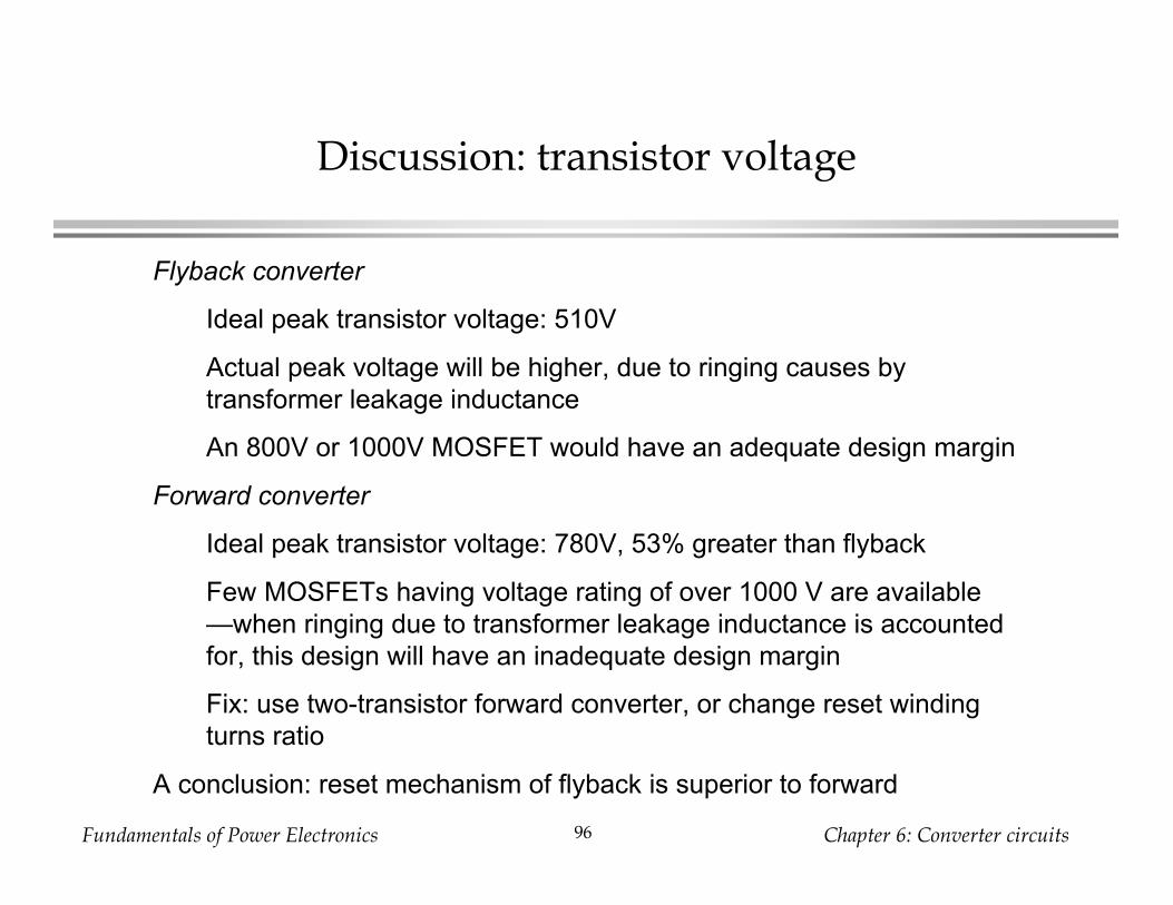
Discussion: transistor voltage
Flyback converter
Ideal peak transistor voltage: 510V
Actual peak voltage will be higher, due to ringing causes bytransformer leakage inductance
An 800V or 1000V MOSFET would have an adequate design margin
Forward converter
Ideal peak transistor voltage: 780V, 53% greater than flyback
Few MOSFETs having voltage rating of over 1000 V are available—when ringing due to transformer leakage inductance is accountedfor, this design will have an inadequate design margin
Fix: use two-transistor forward converter, or change reset windingturns ratio
A conclusion: reset mechanism of flyback is superior to forward

Fundamentals of Power Electronics Chapter 6: Converter circuits97
Discussion: rms transistor current
Forward
1.13A worst-case
transistor utilization 0.226
Flyback
1.38A worst case, 22% higher than forward
transistor utilization 0.284
CCM flyback exhibits higher peak and rms currents. Currents in DCMflyback are even higher

Fundamentals of Power Electronics Chapter 6: Converter circuits98
Discussion: secondary-side diode and capacitor stresses
Forward
peak diode voltage 49V
rms diode current 9.1A / 11.1A
rms capacitor current 1.15A
Flyback
peak diode voltage 64V
rms diode current 16.3A
peak diode current 22.2A
rms capacitor current 9.1A
Secondary-side currents, especially capacitor currents, limit thepractical application of the flyback converter to situations where the loadcurrent is not too great.

Fundamentals of Power Electronics Chapter 7: AC equivalent circuit modeling1
Part IIConverter Dynamics and Control
7. AC equivalent circuit modeling8. Converter transfer functions9. Controller design10. Ac and dc equivalent circuit modeling of the
discontinuous conduction mode11. Current programmed control
Fundamentals of Power Electronics Chapter 7: AC equivalent circuit modeling2
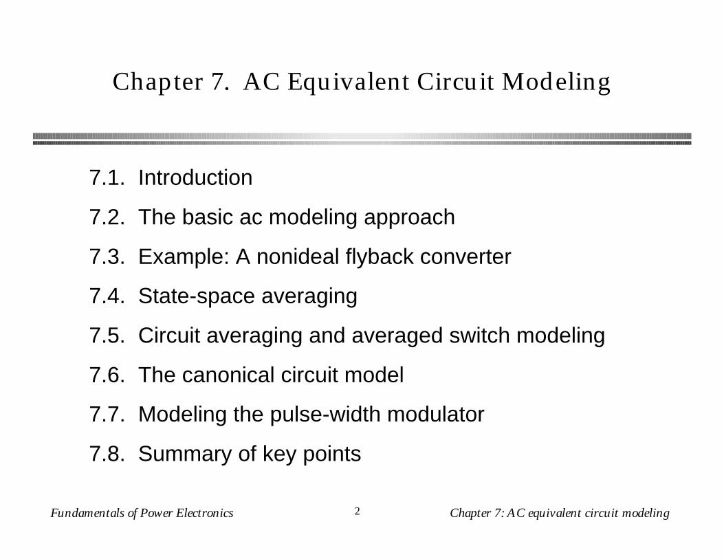
Chapter 7. AC Equivalent Circuit Modeling
7.1. Introduction
7.2. The basic ac modeling approach
7.3. Example: A nonideal flyback converter
7.4. State-space averaging
7.5. Circuit averaging and averaged switch modeling
7.6. The canonical circuit model
7.7. Modeling the pulse-width modulator
7.8. Summary of key points
Fundamentals of Power Electronics Chapter 7: AC equivalent circuit modeling3
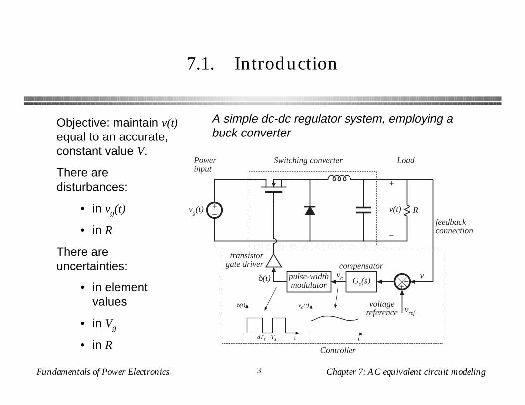
7.1. Introduction
+–
+
v(t)
–
vg(t)
Switching converterPowerinput
Load
–+
R
compensator
Gc(s)
vrefvoltage
reference
v
feedbackconnection
pulse-widthmodulator
vc
transistorgate driver
δ(t)
δ(t)
TsdTs t t
vc(t)
Controller
A simple dc-dc regulator system, employing a buck converter
Objective: maintain v(t) equal to an accurate, constant value V.
There are disturbances:
• in vg(t)
• in R
There are uncertainties:
• in element values
• in Vg
• in R

Fundamentals of Power Electronics Chapter 7: AC equivalent circuit modeling4
Applications of control in power electronics
Dc-dc converters
Regulate dc output voltage.
Control the duty cycle d(t) such that v(t) accurately follows a reference signal vref.
Dc-ac inverters
Regulate an ac output voltage.
Control the duty cycle d(t) such that v(t) accurately follows a reference signal vref (t).
Ac-dc rectifiers
Regulate the dc output voltage.
Regulate the ac input current waveform.
Control the duty cycle d(t) such that ig (t) accurately follows a reference signal iref (t), and v(t) accurately follows a reference signal vref.

Fundamentals of Power Electronics Chapter 7: AC equivalent circuit modeling5
Objective of Part II
Develop tools for modeling, analysis, and design of converter control systems
Need dynamic models of converters:
How do ac variations in vg(t), R, or d(t) affect the output voltage v(t)?
What are the small-signal transfer functions of the converter?
• Extend the steady-state converter models of Chapters 2 and 3, to include CCM converter dynamics (Chapter 7)
• Construct converter small-signal transfer functions (Chapter 8)
• Design converter control systems (Chapter 9)
• Model converters operating in DCM (Chapter 10)
• Current-programmed control of converters (Chapter 11)

Fundamentals of Power Electronics Chapter 7: AC equivalent circuit modeling6
Modeling
• Representation of physical behavior by mathematical means
• Model dominant behavior of system, ignore other insignificant phenomena
• Simplified model yields physical insight, allowing engineer to design system to operate in specified manner
• Approximations neglect small but complicating phenomena
• After basic insight has been gained, model can be refined (if it is judged worthwhile to expend the engineering effort to do so), to account for some of the previously neglected phenomena

Fundamentals of Power Electronics Chapter 7: AC equivalent circuit modeling7
Neglecting the switching ripple
t
t
gatedrive
actual waveform v(t)including ripple
averaged waveform <v(t)>Tswith ripple neglected
d(t) = D + Dm cos ωmt
Suppose the duty cycle is modulated sinusoidally:
where D and Dm are constants, | Dm | << D , and the modulation frequency ωm is much smaller than the converter switching frequency ωs = 2πfs.
The resulting variations in transistor gate drive signal and converter output voltage:
Fundamentals of Power Electronics Chapter 7: AC equivalent circuit modeling8
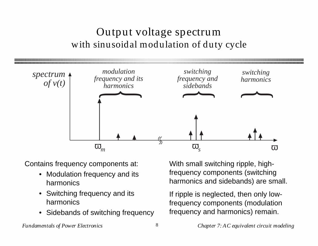
Output voltage spectrumwith sinusoidal modulation of duty cycle
spectrumof v(t)
ωm ωs ω
{modulationfrequency and its
harmonics {switchingfrequency and
sidebands {switchingharmonics
Contains frequency components at:• Modulation frequency and its
harmonics
• Switching frequency and its harmonics
• Sidebands of switching frequency
With small switching ripple, high-frequency components (switching harmonics and sidebands) are small.
If ripple is neglected, then only low-frequency components (modulation frequency and harmonics) remain.

Fundamentals of Power Electronics Chapter 7: AC equivalent circuit modeling9
Objective of ac converter modeling
• Predict how low-frequency variations in duty cycle induce low-frequency variations in the converter voltages and currents
• Ignore the switching ripple
• Ignore complicated switching harmonics and sidebands
Approach:
• Remove switching harmonics by averaging all waveforms over one switching period
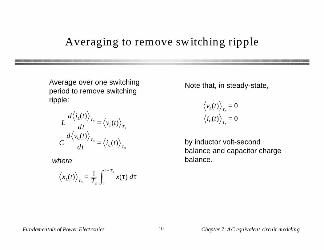
Fundamentals of Power Electronics Chapter 7: AC equivalent circuit modeling10
Averaging to remove switching ripple
Ld iL(t) Ts
dt= vL(t) Ts
Cd vC(t)
Ts
dt= iC(t)
Ts
xL(t) Ts= 1
Tsx(τ) dτ
t
t + Ts
where
Average over one switching period to remove switching ripple:
Note that, in steady-state,
vL(t) Ts= 0
iC(t)Ts
= 0
by inductor volt-second balance and capacitor charge balance.

Fundamentals of Power Electronics Chapter 7: AC equivalent circuit modeling11
Nonlinear averaged equations
Ld iL(t) Ts
dt= vL(t) Ts
Cd vC(t)
Ts
dt= iC(t)
Ts
The averaged voltages and currents are, in general, nonlinear functions of the converter duty cycle, voltages, and currents. Hence, the averaged equations
constitute a system of nonlinear differential equations.
Hence, must linearize by constructing a small-signal converter model.

Fundamentals of Power Electronics Chapter 7: AC equivalent circuit modeling12
Small-signal modeling of the BJT
iBβFiB
βRiBB
C
E
iB
B
C
E
βFiB
rE
Nonlinear Ebers-Moll model Linearized small-signal model, active region

Fundamentals of Power Electronics Chapter 7: AC equivalent circuit modeling13
Buck-boost converter:nonlinear static control-to-output characteristic
D
V
–Vg
0.5 100
actualnonlinear
characteristic
linearizedfunction
quiescentoperatingpoint Example: linearization
at the quiescent operating point
D = 0.5

Fundamentals of Power Electronics Chapter 7: AC equivalent circuit modeling14
Result of averaged small-signal ac modeling
+– I d(t)vg(t)
+–
LVg – V d(t)
+
v(t)
–
RCI d(t)
1 : D D' : 1
Small-signal ac equivalent circuit model
buck-boost example


