Abstract - In this paper, 32 bit SRAM Architecture design using 90nm CMOS technology has been proposed. The SRAM architecture includes 6T Memory cell, precharge circuit, write driver, address decoder, sense amplifier respectively. Total power dissipation of 195.81 µW to 666.6 µW is obtained from 90nm to 45nm technology. Area from 19.22 µm2 to15.5775 µm2 for 90nm to 45nm technology is observed. Testing and simulation is carried out in LTspice and layout is implemented in Microwind 3.5 tool using 90nm CMOS technology.
Key Words: Static Random Access Memory (SRAM), 6T memory cell, area, power dissipation, 90nm-45nm.
1. INTRODUCTION In recent years, the explosive growth of battery operated devices has made the low power memory design an urge in the industry. As transistor count increases the leakage current have made the SRAM unit a power hungry block from both the static and dynamic perspectives. Also the SRAM block is an important part in SOC design nowadays. Here the power dissipation and area are the main factors in designing the memory. In memory designing, scaling of memory density must continue to track the scaling trends of logic. Here in the proposed SRAM architecture the experimental results are implemented in 90nm to 45nm CMOS technology confirmed the concept of SRAM design. In Section II, Design strategies for SRAM cell is explained. Section III. SRAM architecture is explained in detail. In Section IV, Experimental results are shown. In Section V, performance parameters are obtained. In Section VI the paper is concluded.
2. DESIGN STRATEGIES FOR SRAM CELL
To determine the (W/L) ratio of the transistors in a SRAM cell the basic requirements must be taken into consideration. i. In SRAM cell, the data operation should not destroy
the stored information. ii. It should allow the modification of the stored data
during data-write phase.
Noise margin is the maximum voltage that can be added to the logic gate which does not affect the output of logic gate.For stability of the SRAM cell,good SNM is required that depends on the value of CR and PR. Cell Ratio is the ratio between sizes of driver transistors to the load transistors during read operation. CR=(W1/L1)/(W5/L5) Pull-up ratio is the ratio between sizes of the load transistor to access transistor during write operation. PR=(W4/L4)/(W6/L6). NM which affects both,read and write margin.it is related to threshold voltages of the PMOS and NMOS devices also.for higher NM,the threshold voltages should also be increased.if it is too much high then it will be difficult to operate as it is hard to flip the operation of MOS devices.we get different speed by changing the cell ratio.as cell ratio increases the size of the driver transistor also increases and the current increases.by changing the value of CR, we get different NM for different technology.
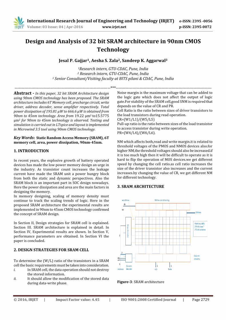
3. SRAM ARCHITECTURE
Figure-3: SRAM architecture
International Research Journal of Engineering and Technology (IRJET) e-ISSN: 2395 -0056
Figure.3 shows 32 bit SRAM architecture which consists of the basic 6T memory cell. Each bit is accessed using a 5 bit address word, with 3 bits of row selection and 2 bits for column decoding. For a compact layout, the row decoder should be pitch matched to the SRAM cell height and the predecode circuits can be placed below or adjacent to the row decode circuits. The column decoder selects one column to read the cell voltage via sense amplifier onto the corresponding bit lines. Here only one sense amplifier is used. The row decode, read strobe and the write strobe for the column decoders are qualified by appropriate non-overlapping clock phase(φ1) to synchronize the read and write access.Bitline precharge circuitry are placed above each column and qualified by clock phase φ2.The column mux,data write and sense amplifier circuits are placed below the SRAM core.
3.1 6T memory cell
Figure-3.1 (a): Schematic diagram of 6T memory cell
Figure-3.1 (b): output waveform of 6T memory cell
It is used for low power, low voltage operations. Here it uses bistable latching circuitry to store each bit. In Figure.3.1 (a) M1 and M2 PMOS are the pull up transistors whereas M3 and M4 NMOS are the driver transistors. Access is enabled by word line which is connected to M5 and M6 pass transistors which gives BL and BLB lines which are used for both reading and writing purpose. These bit lines improve the noise margin. Differential circuitry gives advantage of
detectable output voltage swings.it stores logic 0 or 1 as far as the power is on so it do not need to be refreshed unlike DRAM cells. . [4] Here in SRAM design, the transistors’ size is of most importance to its right operation. Starting by inverters, here the width of NMOS of 0.09um and since the NMOS are approximately twice as conductive as the PMOS.W=0.18um is taken to balance their conductivity. On the other hand, the gateway transistors must be 2 or 3 times larger than the NMOS transistors from the inverters, so that they are conductive enough to change the logic level stored by these transistors. However they should not be much larger so that they won’t occupy much space. I opted for a width of 0.18um for these gateway transistors.Figure.3.1 (b) shows the output waveform of the 6T memory cell.
3.2 Precharge circuit
Figure-3.2 (a): Schematic diagram of Precharge circuit
Figure-3.2 (b): output waveform of Precharge circuit
Precharge circuit is used for read and write operation for
precharging and equalizing the bit line and bit line bar lines.
Here it can be done by M1 and M2 PMOS transistors those
will precharge the operation and M3 PMOS transistor is used
to equalize the operation here Vdd is given in this
input.Figure.3.2(a) shows the schematic diagram of
precharge circuitry and Vdd=1v is taken here.Figure.3.2(b)
shows the output waveform of the precharge circuitry.
3.3 Sense amplifier The sense amplifier amplifies a small analog differential voltage developed on the bit lines in a read access.The
International Research Journal of Engineering and Technology (IRJET) e-ISSN: 2395 -0056
amplification results in a full swing single ended digital output.Employment of SA reduces the size of the SRAM cell since the drive transistors does not need to fully discharge the bit lines.Generally read operations are the slowest which gives delay in the cell.Bit lines has larger capacitance due to metal length and number of transistors that will consume greater amount of time to discharge the bit lines.Here timing control and load capacitor selection are the difficult choice for sense amplifier.For that SAE signal is used.Here latch type sense amplifier is used in which two cross coupled inverters are used which gives the differential output that amplifies the signal and gives full swings and two capacitors which stores the level of the bit lines. . [4]
Figure-3.3 (a): Schematic diagram of Sense amplifier
Figure-3.3 (b): output waveform of Sense amplifier
In Figure.3.3 (a) sense amplifier has W=0.09um for NMOS
and W=0.18um for PMOS, with the exception of one NMOS
transistor that connects to Vss, simply to make use of space
that was available. An inverter will activate all the PMOS
transistors connected to Vdd. [4].Figure.3.3 (b) shows the
output waveform of the sense amplifier.
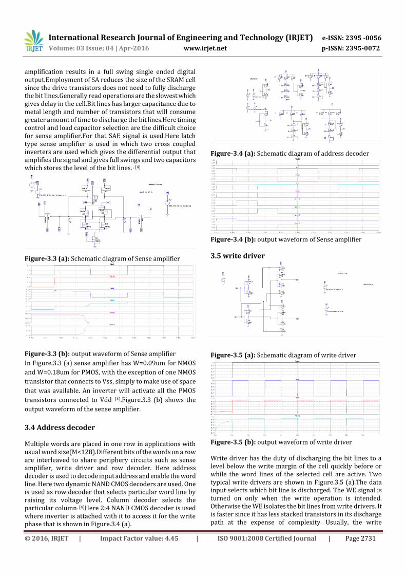
3.4 Address decoder Multiple words are placed in one row in applications with usual word size(M<128).Different bits of the words on a row are interleaved to share periphery circuits such as sense amplifier, write driver and row decoder. Here address decoder is used to decode input address and enable the word line. Here two dynamic NAND CMOS decoders are used. One is used as row decoder that selects particular word line by raising its voltage level. Column decoder selects the particular column. [4]Here 2:4 NAND CMOS decoder is used where inverter is attached with it to access it for the write phase that is shown in Figure.3.4 (a).
Figure-3.4 (a): Schematic diagram of address decoder
Figure-3.4 (b): output waveform of Sense amplifier
3.5 write driver
Figure-3.5 (a): Schematic diagram of write driver
Figure-3.5 (b): output waveform of write driver Write driver has the duty of discharging the bit lines to a level below the write margin of the cell quickly before or while the word lines of the selected cell are active. Two typical write drivers are shown in Figure.3.5 (a).The data input selects which bit line is discharged. The WE signal is turned on only when the write operation is intended. Otherwise the WE isolates the bit lines from write drivers. It is faster since it has less stacked transistors in its discharge path at the expense of complexity. Usually, the write
International Research Journal of Engineering and Technology (IRJET) e-ISSN: 2395 -0056
operation is not a speed limiting transaction and therefore, simpler configurations relaxing the layout requirements are preferred for the write driver. It is made up of CMOS inverter and NMOS pass transistors and it can be sized up as it does not depend on the number of transistors to form a column. . [4]
4. EXPERIMENTAL RESULTS
4. 1 Layout In these section layout is carried out using microwind 3.5 tool of different sub blocks and also the 1*1 bit SRAM and finally 32 bit SRAM unit is shown below.
Figure-4.1: layout of 6T memory cell
Figure-4.2: layout of precharge circuit
Figure-4.3: layout of sense amplifier
Figure-4.4: layout of address decoder
Figure-4.5: layout of 1*1 bit SRAM In Figure.4.5 Besides the previous elements 2 more transistors were added to select between the operation, connecting the bit lines with the data in or out terminals. This is necessary for simulation purposes since the line and column decoders as well as the I/O buffers have not designed. As such 2 new inputs have also been created the write enable input and the read enable input which when
International Research Journal of Engineering and Technology (IRJET) e-ISSN: 2395 -0056
high, will turn on their respective transistor, selecting the line for input and output of the data.
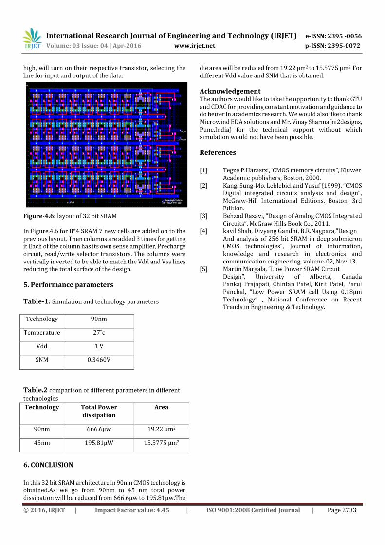
Figure-4.6: layout of 32 bit SRAM In Figure.4.6 for 8*4 SRAM 7 new cells are added on to the previous layout. Then columns are added 3 times for getting it.Each of the column has its own sense amplifier, Precharge circuit, read/write selector transistors. The columns were vertically inverted to be able to match the Vdd and Vss lines reducing the total surface of the design.
5. Performance parameters Table-1: Simulation and technology parameters
Technology 90nm
Temperature 27˚c
Vdd 1 V
SNM 0.3460V
Table.2 comparison of different parameters in different
technologies
Technology Total Power
dissipation
Area
90nm 666.6µw 19.22 µm2
45nm 195.81µW 15.5775 µm2
6. CONCLUSION
In this 32 bit SRAM architecture in 90nm CMOS technology is obtained.As we go from 90nm to 45 nm total power dissipation will be reduced from 666.6µw to 195.81µw.The
die area will be reduced from 19.22 µm2 to 15.5775 µm2. For different Vdd value and SNM that is obtained.
Acknowledgement The authors would like to take the opportunity to thank GTU and CDAC for providing constant motivation and guidance to do better in academics research. We would also like to thank Microwind EDA solutions and Mr. Vinay Sharma(ni2designs, Pune,India) for the technical support without which simulation would not have been possible.
Academic publishers, Boston, 2000. [2] Kang, Sung-Mo, Leblebici and Yusuf (1999), “CMOS
Digital integrated circuits analysis and design”, McGraw-Hill International Editions, Boston, 3rd Edition.
[3] Behzad Razavi, “Design of Analog CMOS Integrated Circuits”, McGraw Hills Book Co., 2011.
[4] kavil Shah, Divyang Gandhi, B.R.Nagpara,”Design And analysis of 256 bit SRAM in deep submicron CMOS technologies”, Journal of information, knowledge and research in electronics and communication engineering, volume-02, Nov 13.
[5] Martin Margala, “Low Power SRAM Circuit Design”, University of Alberta, Canada Pankaj Prajapati, Chintan Patel, Kirit Patel, Parul Panchal, “Low Power SRAM cell Using 0.18µm Technology” , National Conference on Recent Trends in Engineering & Technology.