Design and Implementation of a
Modular Multilevel Converter
Prepared by:
Jesse Doerksen
Joel Taylor
Final Report submitted in partial satisfaction
of the requirements for the degree of
Bachelor of Science
in
Electrical Engineering
in the
Faculty of Engineering
of the
University of Manitoba
Faculty Supervisor:
Dr. Shaahin Filizadeh
Course Coordinator:
Dr. Behzad Kori
© Copyright by Jesse Doerksen and Joel Taylor, 2013.
i
Abstract
This report describes the design and implementation of a single phase modular multilevel
converter (MMC). MMC is a converter used for converting AC to DC voltage and vice versa.
MMC can be used in a multitude of applications, including HVDC transmission because of its
high power ratings and low total harmonic distortion.
This report is divided into two main sections, the first being MMC simulation. We
simulated a single-phase 21- level MMC using PSCAD/EMTDC simulator and attained plots of
the results. The results show that our design of a 21-level MMC worked and met our
specifications.
The second main section of our project deals with the implementation of an MMC. We
first tried to implement a 21 - level MMC but encountered problems in providing the correct gate
voltages to our MOSFETS. We finished the project by using low power optocouplers and
byproviding the positive half of the waveform that a fully functional MMC would produce.
ii
Contributions
This project demonstrates the waveform obtained by using an MMC for voltage
rectification and inversion in high voltage systems. This technology is a new method in voltage
conversion that has great potential to be used in high voltage applications all over the world. Both
team members contributed significantly to this project in order to achieve the project goals.
However, the project was divided up into two main sections.
- Software design and simulation
- Hardware design and implementation
Jesse was primarily responsible for the software design and testing because of his
extensive background knowledge in PSCAD and RSCAD. Joel was primarily responsible for the
hardware design and implementation because of his hands on experience in circuit building.
iii
Acknowledgements
The authors of this report would like to acknowledge the assistance and support of
several people that helped us throughout the course of this project.
We would like to thank our supervising professor Dr. Shaahin Filizadeh for giving us the
chance to work on his undergraduate project and for all the time he spent with us designing and
troubleshooting our controller and for reading through all our reports and offering valuable advice
and comments.
We would also like to thank Erwin Dirks from the power system group at the University
of Manitoba for the ideas and suggestions he gave us along with the hardware he provided us
with.
We would like to thank the electrical engineering technical shop for assisting us in
ordering hardware and for providing hardware that the technical shop has in stock.
We would like to thank Gary Bistyak and Arash Darbandi for the problem solving and
advise they gave us in regards to hardware implementation.
iv
Table of Contents
List of Figures ................................................................................................................................ vii
List of Tables ................................................................................................................................ viii
Nomenclature .................................................................................................................................. ix
1.0 Introduction .......................................................................................................................... 1
2.0 System Overview ................................................................................................................. 3
2.1 MMC Circuitry ................................................................................................................ 3
2.2 Principles of Power Flow in AC Systems ........................................................................ 5
2.3 Specifications for the MMC Design ................................................................................ 6
3.0 System Design ..................................................................................................................... 8
3.1 Number of Levels ............................................................................................................ 8
3.2 Development of a Model in Simulink ............................................................................ 11
3.3 Calculated Component Values ....................................................................................... 12
3.4 Measurement System ..................................................................................................... 13
3.5 Power Flow Control ....................................................................................................... 14
3.6 Nearest Level Control .................................................................................................... 14
3.7 Balancing Control Algorithm......................................................................................... 15
4.0 Electromagnetic Transient Simulation of an MMC ........................................................... 16
4.1 Tested Component Values ............................................................................................. 16
4.2 Results ............................................................................................................................ 17
4.2.1 Capacitor Voltage Regulation ................................................................................ 17
4.2.2 Total Harmonic Distortion ..................................................................................... 17
v
4.2.3 Power Step ............................................................................................................. 18
4.2.4 Power Reversal ...................................................................................................... 19
5.0 Circuit Hardware ................................................................................................................ 20
5.1 Real Time Simulation of MMC ..................................................................................... 20
5.1.1 RSCAD ......................................................................................................................... 21
5.1.2 RTDS Hardware ..................................................................................................... 21
5.2 Lab-Volt electrical bench ............................................................................................... 23
5.2.1 Data Acquisition Interface ..................................................................................... 24
5.2.2 Power supply and other components ..................................................................... 25
5.3 Component Selection ..................................................................................................... 25
5.3.1 MOSFETs .............................................................................................................. 25
5.3.2 Capacitors .............................................................................................................. 26
5.3.3 Gate Drivers ........................................................................................................... 26
5.3.4 Dead Time Generators ........................................................................................... 26
5.3.5 Inductors ................................................................................................................ 26
5.3.6 Optocouplers .......................................................................................................... 27
6.0 Testing and Simulation Reconciliation .............................................................................. 28
6.1 Components ................................................................................................................... 28
6.1.1 Switches ................................................................................................................. 28
6.1.2 Gate Driver ............................................................................................................. 29
6.1.3 Dead Time Generators ........................................................................................... 29
6.1.4 Capacitors .............................................................................................................. 30
vi
6.1.5 Crystal Oscillator ................................................................................................... 30
6.2 Single Submodule .......................................................................................................... 30
6.3 Five levels ...................................................................................................................... 31
7.0 Future Work ............................................................................................................................. 32
7.1 Increase Levels............................................................................................................... 32
7.2 Three Phase .................................................................................................................... 32
7.3 Complete Hardware Implementation ............................................................................ 33
7.4 Protection ....................................................................................................................... 34
7.5 Printed Circuit Board ..................................................................................................... 34
7.6 Circulating Current Suppressing Controller .................................................................. 35
8.0 Conclusion ......................................................................................................................... 36
Appendix A: Bill of Material ......................................................................................................... 37
Appendix B: PSCAD Design ......................................................................................................... 38
Appendix C: RSCAD Design ........................................................................................................ 40
Appendix D: RSCAD Code ........................................................................................................... 43
References ...................................................................................................................................... 48
Vita................................................................................................................................................. 49
vii
List of Figures
Figure 2-1: Multi-valve .................................................................................................................... 4
Figure 2-2: Submodule .................................................................................................................... 5
Figure 2-3: Power Flow ................................................................................................................... 5
Figure 3-1: Control System Diagram ............................................................................................... 8
Figure 3-2: Total Harmonic Distortion ............................................................................................ 9
Figure 3-3: Inverse of THD ........................................................................................................... 10
Figure 3-4: Simulink Case ............................................................................................................. 11
Figure 3-5: 21-level MMC Waveform ........................................................................................... 12
Figure 4-1: Circuit Schematic ........................................................................................................ 16
Figure 4-2: Capacitor Voltage ....................................................................................................... 17
Figure 4-3:AC voltage and THD ................................................................................................... 18
Figure 4-4:Power Step ................................................................................................................... 19
Figure 4-5:Power Reversal ............................................................................................................ 19
Figure 5-1: Switching Circuit ........................................................................................................ 20
Figure 5-2: Portable RTDS Cubical ............................................................................................... 21
Figure 5-3: GTDO Card ................................................................................................................. 22
Figure 5-4: GTAI Card .................................................................................................................. 23
Figure 5-5: Lab-Volt Setup ............................................................................................................ 24
Figure 6-1: MOSFET Switching Time .......................................................................................... 28
Figure 6-2: Gate driver................................................................................................................... 29
Figure 6-3: Dead Time ................................................................................................................... 30
Figure 6-4: 5-Level Positive Multi-valve....................................................................................... 31
Figure B-1: Main Schematic .......................................................................................................... 38
Figure B-2: MMC Schematic ......................................................................................................... 38
Figure B-3: Multi-valve Schematic ............................................................................................... 39
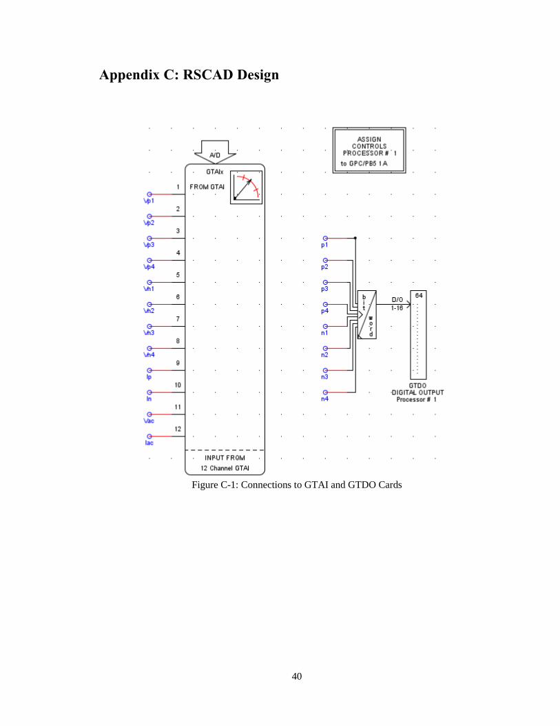
Figure C-1: Connections to GTAI and GTDO Cards .................................................................... 40
Figure C-2: Control System ........................................................................................................... 41
Figure C-3: Measurement System ................................................................................................. 42
viii
List of Tables
Table 2-1: Original Specifications………………………………………………………………14
Table A-1: Bill of Material……………………………………………………………………….37
ix
Nomenclature
AC – Alternating Current
DAI – Data Acquisition Interface
DC – Direct Current
FACTS – Flexible AC Transmission Systems
GTAI – Giga-Transceiver Analog Input
GTDO – Giga-Transceiver Digital Output
HVDC – High Voltage Direct Current
Lb – Base Inductance
MMC – Modular Multilevel Converter
MOSFET – Metal Oxide Semiconductor Field Effect Transistor
MV – Multi-Valve
Nsm – Number of submodules per multi-valve
P – Active Power [W]
PLL – Phase Locked Loop
PSCAD – Power System Computer Aided Design
Q – Reactive Power [var]
RMS – Root Mean Squared
RSCAD – Real System Computer Aided Design
RTDS – Real Time Digital Simulator
S – Apparent Power [VA]
x
Sb – Base Power
SM – Submodule
SSSC – Static Synchronous Series Compensator
STATCOM – Static Compensator
UPFC – Universal Power Flow Controller
Vb – Base Voltage
Vc – Capacitor Voltage
Vgs – Voltage from gate to source (MOSFET)
Vs – Voltage from source to ground (MOSFET)
VSC – Voltage Source Converter
Zb – Base Impedance
1
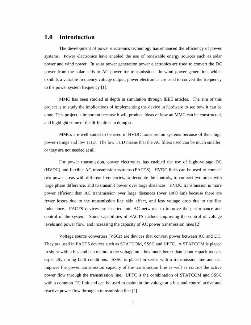
1.0 Introduction
The development of power electronics technology has enhanced the efficiency of power
systems. Power electronics have enabled the use of renewable energy sources such as solar
power and wind power. In solar power generation power electronics are used to convert the DC
power from the solar cells to AC power for transmission. In wind power generation, which
exhibits a variable frequency voltage output, power electronics are used to convert the frequency
to the power system frequency [1].
MMC has been studied in depth in simulation through IEEE articles. The aim of this
project is to study the implications of implementing the device in hardware to see how it can be
done. This project is important because it will produce ideas of how an MMC can be constructed,
and highlight some of the difficulties in doing so.
MMCs are well suited to be used in HVDC transmission systems because of their high
power ratings and low THD. The low THD means that the AC filters used can be much smaller,
or they are not needed at all.
For power transmission, power electronics has enabled the use of hight-voltage DC
(HVDC) and flexible AC transmission systems (FACTS). HVDC links can be used to connect
two power areas with different frequencies, to decouple the controls, to connect two areas with
large phase difference, and to transmit power over large distances. HVDC transmission is more
power efficient than AC transmission over large distances (over 1000 km) because there are
fewer losses due to the transmission line skin effect, and less voltage drop due to the line
inductance. FACTS devices are inserted into AC networks to improve the performance and
control of the system. Some capabilities of FACTS include improving the control of voltage
levels and power flow, and increasing the capacity of AC power transmission lines [2].
Voltage source converters (VSCs) are devices that convert power between AC and DC.
They are used in FACTS devices such as STATCOM, SSSC and UPFC. A STATCOM is placed
in shunt with a bus and can maintain the voltage on a bus much better than shunt capacitors can,
especially during fault conditions. SSSC is placed in series with a transmission line and can
improve the power transmission capacity of the transmission line as well as control the active
power flow through the transmission line. UPFC is the combination of STATCOM and SSSC
with a common DC link and can be used to maintain the voltage at a bus and control active and
reactive power flow through a transmission line [2].
2
There are several types of VSCs including 2-level, multi-level and MMC. 2-level VSCs
are simple to implement and have few components, just 6 switches with reverse diodes per three-
phase bridge. The problem with 2-level VSCs is the harmonic content, which requires
complicated modulation techniques and/or AC filters. Since the maximum reverse voltage of
each switch in a 2-level VSC is large, the overall power ratings of 2-level converters is limited to
the ratings of the switches and diodes, and thus series and shunt combinations of devices need to
be employed to achieve the desired voltage and current ratings. Multilevel converters use a
variety of circuit configurations to produce higher level voltage waveforms, but the number of
components required to build them is exponentially proportional to the number of levels. There is
a compromise between the number of components and the harmonics. Increasing the number of
levels decreases the total harmonic distortion (THD) because a closer approximation to a
sinusoidal waveform is obtained.
The MMC has several advantages on 2-level and multilevel VSCs. MMCs have
cascaded switches, such that the maximum reverse voltage is smaller; therefore, the power ratings
of MMC can be much larger. The number of components needed in an MMC is linearly
proportional to the number of levels, which is a considerable advantage over multilevel VSCs.
MMCs can be constructed with hundreds of levels without adding complexity, therefore
decreasing the THD of the voltage waveform dramatically.
3
2.0 System Overview
An overview of this project is given to break down of what is included in an MMC circuit
and how it is connected together to get a fully functional MMC. This chapter also includes the
principles of power flow and the specifications for our MMC design.
2.1 MMC Circuitry
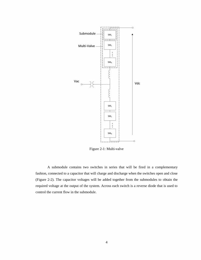
An MMC is a circuit that can be used to convert AC to DC voltage and convert DC to
AC voltage. It is generally used in high voltage engineering because it has the ability to work at
multiple voltage levels. The MMC is made up of two multi-valves, one for the positive voltages
called the upper multi-valve and the other for the negative voltages called the lower multi-valve.
These two multi-valves as shown in Figure 2-1 are connected together through two inductors to
control the power flow. Each multi-valve contains multiple submodules that are cascaded
together. The more submodules in each multi-valve the higher the voltage it can convert and the
smoother the AC waveform will be.
4
Figure 2-1: Multi-valve
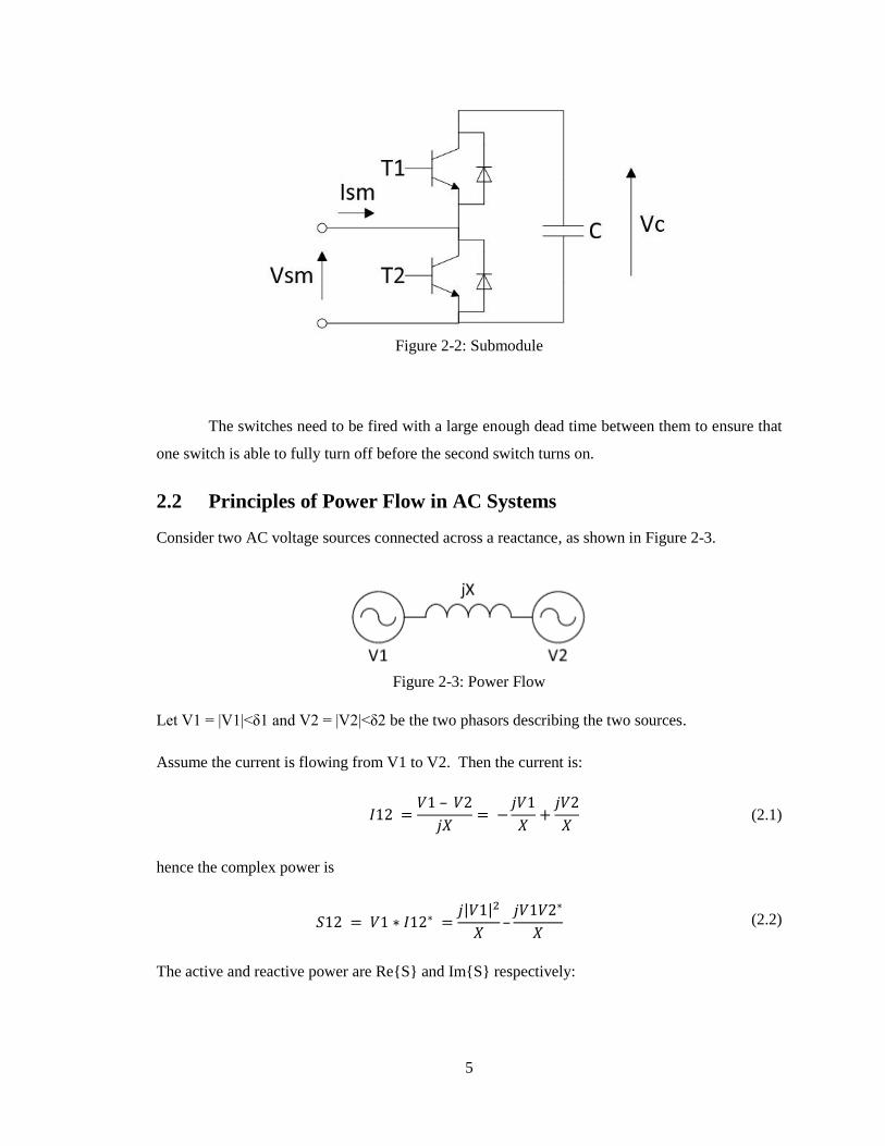
A submodule contains two switches in series that will be fired in a complementary
fashion, connected to a capacitor that will charge and discharge when the switches open and close
(Figure 2-2). The capacitor voltages will be added together from the submodules to obtain the
required voltage at the output of the system. Across each switch is a reverse diode that is used to
control the current flow in the submodule.
5
Figure 2-2: Submodule
The switches need to be fired with a large enough dead time between them to ensure that
one switch is able to fully turn off before the second switch turns on.
2.2 Principles of Power Flow in AC Systems
Consider two AC voltage sources connected across a reactance, as shown in Figure 2-3.
Figure 2-3: Power Flow
Let V1 = |V1|<δ1 and V2 = |V2|<δ2 be the two phasors describing the two sources.
Assume the current is flowing from V1 to V2. Then the current is:
(2.1)
hence the complex power is
| |
(2.2)
The active and reactive power are ReS and ImS respectively:
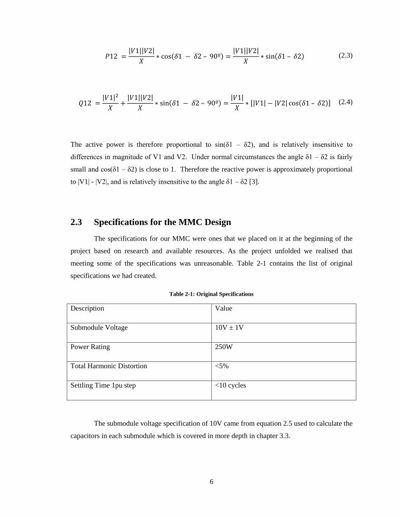
6
| || |
( )
| || |
( ) (2.3)
| |
| || |
( )
| |
[| | | | ( )] (2.4)
The active power is therefore proportional to sin(δ1 – δ2), and is relatively insensitive to
differences in magnitude of V1 and V2. Under normal circumstances the angle δ1 – δ2 is fairly
small and cos(δ1 – δ2) is close to 1. Therefore the reactive power is approximately proportional
to |V1| - |V2|, and is relatively insensitive to the angle δ1 – δ2 [3].
2.3 Specifications for the MMC Design
The specifications for our MMC were ones that we placed on it at the beginning of the
project based on research and available resources. As the project unfolded we realised that
meeting some of the specifications was unreasonable. Table 2-1 contains the list of original
specifications we had created.
Table 2-1: Original Specifications
Description Value
Submodule Voltage 10V ± 1V
Power Rating 250W
Total Harmonic Distortion <5%
Settling Time 1pu step <10 cycles
The submodule voltage specification of 10V came from equation 2.5 used to calculate the
capacitors in each submodule which is covered in more depth in chapter 3.3.
7
(2.5)
The variance of 1V is a voltage level that we thought would be appropriate and
reasonable for us to achieve.
We selected the power rating specification based on the existing laboratory benches (Lab-
Volt set up) which has a power rating of 250W on most of its components. As explained in the
following chapters we did not need to use the Lab-Volt setup so this rating is no longer necessary.
We selected total harmonic distortion and settling time specifications based on reasonable
values on simulations that we had already run and improvements on those simulations that we
intended on doing.
8
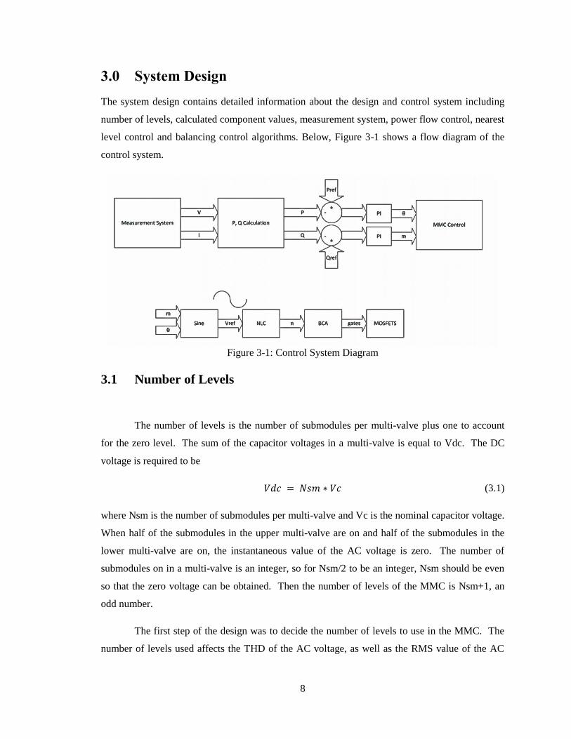
3.0 System Design
The system design contains detailed information about the design and control system including
number of levels, calculated component values, measurement system, power flow control, nearest
level control and balancing control algorithms. Below, Figure 3-1 shows a flow diagram of the
control system.
Figure 3-1: Control System Diagram
3.1 Number of Levels
The number of levels is the number of submodules per multi-valve plus one to account
for the zero level. The sum of the capacitor voltages in a multi-valve is equal to Vdc. The DC
voltage is required to be
(3.1)
where Nsm is the number of submodules per multi-valve and Vc is the nominal capacitor voltage.
When half of the submodules in the upper multi-valve are on and half of the submodules in the
lower multi-valve are on, the instantaneous value of the AC voltage is zero. The number of
submodules on in a multi-valve is an integer, so for Nsm/2 to be an integer, Nsm should be even
so that the zero voltage can be obtained. Then the number of levels of the MMC is Nsm+1, an
odd number.
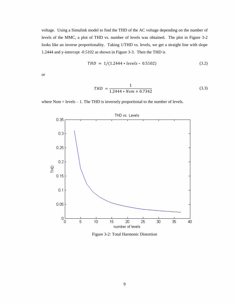
The first step of the design was to decide the number of levels to use in the MMC. The
number of levels used affects the THD of the AC voltage, as well as the RMS value of the AC
9
voltage. Using a Simulink model to find the THD of the AC voltage depending on the number of
levels of the MMC, a plot of THD vs. number of levels was obtained. The plot in Figure 3-2
looks like an inverse proportionality. Taking 1/THD vs. levels, we get a straight line with slope
1.2444 and y-intercept -0.5102 as shown in Figure 3-3. Then the THD is
( ) (3.2)
or
(3.3)
where Nsm = levels – 1. The THD is inversely proportional to the number of levels.
Figure 3-2: Total Harmonic Distortion
10
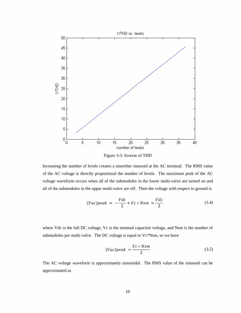
Figure 3-3: Inverse of THD
Increasing the number of levels creates a smoother sinusoid at the AC terminal. The RMS value
of the AC voltage is directly proportional the number of levels. The maximum peak of the AC
voltage waveform occurs when all of the submodules in the lower multi-valve are turned on and
all of the submodules in the upper multi-valve are off. Then the voltage with respect to ground is
( )
(3.4)
where Vdc is the full DC voltage, Vc is the nominal capacitor voltage, and Nsm is the number of
submodules per multi-valve. The DC voltage is equal to Vc*Nsm, so we have
( )
(3.5)
The AC voltage waveform is approximately sinusoidal. The RMS value of the sinusoid can be
approximated as
11
( )
(3.6)
with Vc = 10.0 V this is
(3.7)
A Simulink model is used to find an aproprate number of levels to use in the system.
3.2 Development of a Model in Simulink
In order to find the THD of the AC voltage waveform, a Simulink simulation is used as
shown is Figure 3-4.
Figure 3-4: Simulink Case
The AC voltage waveform is created by using a rounding function on a 60 Hz sine wave
as per the NLC modulation technique (which will be covered in detail in section 3.7). The THD
is found using the Total Harmonic Distortion block from the SimPowerSystems toolkit, in the
Extras/Signal Measurements section. The fundamental frequency of the THD measurement block
is set to 60 Hz. The RMS voltage is found using the RMS block from the same section. The
fundamental frequency of the RMS block is set to 60 Hz. The RMS current is found by dividing
the rated active power Prated by the RMS voltage, since P = Vrms*Irms. Prated = 250.0 W.
12
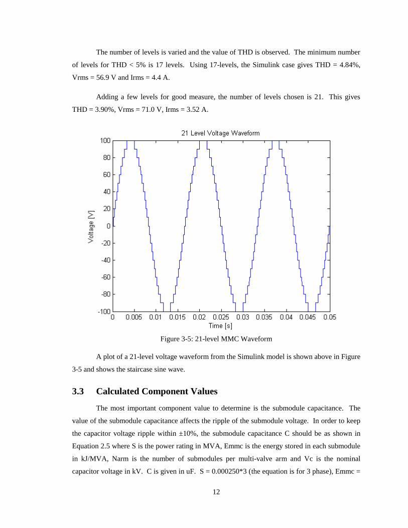
The number of levels is varied and the value of THD is observed. The minimum number
of levels for THD < 5% is 17 levels. Using 17-levels, the Simulink case gives THD = 4.84%,
Vrms = 56.9 V and Irms = 4.4 A.
Adding a few levels for good measure, the number of levels chosen is 21. This gives
THD = 3.90%, Vrms = 71.0 V, Irms = 3.52 A.
Figure 3-5: 21-level MMC Waveform
A plot of a 21-level voltage waveform from the Simulink model is shown above in Figure
3-5 and shows the staircase sine wave.
3.3 Calculated Component Values
The most important component value to determine is the submodule capacitance. The
value of the submodule capacitance affects the ripple of the submodule voltage. In order to keep
the capacitor voltage ripple within ±10%, the submodule capacitance C should be as shown in
Equation 2.5 where S is the power rating in MVA, Emmc is the energy stored in each submodule
in kJ/MVA, Narm is the number of submodules per multi-valve arm and Vc is the nominal
capacitor voltage in kV. C is given in uF. S = 0.000250*3 (the equation is for 3 phase), Emmc =
13
30-40, Narm = 20, Vc = 0.010. This gives C = 3.75-5 mF. The value 4.7mF is chosen because
the hardware was available.
The transformer power rating was chosen to be 250 VA as per specification. The leakage
reactance was chosen to be 10%. It was desired to have a primary voltage of 120 V. The
maximum voltage that the 21 level MMC can produce at the secondary side of the transformer is
71.0 V. The secondary voltage was chosen to be less than 71.0 V so that the MMC is capable of
sending reactive power to the AC side. The secondary voltage was chosen to be 60.0 V. The
modulation index m used in order to have the MMC AC voltage at 60.0 V is 60.0/71.0 = 0.845.
The number of levels used to attain this voltage is 0.845*21 = 17.745 > 17 so the THD
requirement is still met.
The value of the arm inductors were chosen as 15% the system base [4]. The base
impedance on the secondary side of the transformer is:
(3.8)
where Vb = secondary voltage = 60 V and Sb = power rating = 250 VA. This gives Zb = 14.4 Ω.
Then
(3.9)
where w is the frequency = 2π60. Lb = 38.2 mH. Taking 15% of the base inductance we have
Larm = 5.7 mH.
3.4 Measurement System
The measurement system needs to measure the instantaneous arm currents and the
instantaneous AC voltage and current. The active and reactive power flow is calculated from the
instantaneous voltage and current. The positive direction for the power measurement is from DC
to AC. Treating the voltage and current signals as digital signals, the RMS values can be found
with the equation
√
( ) (3.10)
14
A phase-lock loop (PLL) is used to obtain the voltage phase angle θ on the primary side of the
transformer. Another PLL is used to obtain the current phase angle φ. Then the apparent power
can be calculated as
(3.11)
and the active and reactive power are
(𝜃 𝜑) (3.12)
(𝜃 𝜑) (3.13)
The P and Q values are passed to the power flow controller so that the power can be
monitored and controlled.
3.5 Power Flow Control
In order to control the active and reactive power in a closed loop configuration, PI
controllers are used. The active power mostly depends on the voltage phase difference across the
transformer δ. The active power is directly proportional to sinδ. A PI controller can be used with
the active power error Pref-P at the input, where Pref is the reference active power and P is the
active power measurement, in pu. The output of this PI controller is the desired phase angle δ. If
P < Pref, the Perror is positive and δ increases, correcting the error. If P > Pref, Perror is negative
and δ decreases, correcting the error. The reactive power depends mostly on the difference in
magnitude of the phase voltages. Reactive power flows from the side with higher magnitude of
voltage to the side with lower magnitude of voltage. A PI controller can be used with reactive
power error Qref-Q at the input, where Qref is the reference reactive power and Q is the measured
reactive power, in pu. The output of this PI controller is the modulation index m, which scales
the magnitude of the AC voltage at the secondary. If Q<Qref, Qerror is positive and m increases,
correcting the error. If Q>Qref, Qerror is negative and m decreases, correcting the error. The
modulation index m is limited between 0 and 1. The PI controllers were tuned manually in the
simulation.
3.6 Nearest Level Control
Nearest level control (NLC) is a modulation technique used to control the number of
submodules to turn on in a multi-valve. This modulation technique was chosen for its simplicity
and effectiveness. The input of the NLC is the reference voltage waveform. The reference
voltage waveform is a sine wave with the amplitude scaled by the modulation index m and with
15
phase (δ+θ). The frequency of the reference voltage waveform is 60 Hz. The maximum
amplitude of the reference voltage waveform is equal to the maximum peak voltage, Vdc/2 =
100V. The NLC is a quantizer that rounds the reference voltage waveform to the nearest
available level according to the nominal capacitor voltage [5]. The nominal capacitor voltage is
10 V, so the reference voltage waveform is rounded to the nearest value 10n, where n is an
integer. Then the number of submodules to turn on in the lower multi-valve is
(3.14)
and the number of submodules to turn on in the upper multi-valve is
(3.15)
The values from equations 3.14 and 3.15 are passed to the balancing control algorithm.
3.7 Balancing Control Algorithm
Since the arm currents can flow in either direction, the submodule capacitors voltage
change when the submodule is turned on. When Imv is positive, the capacitor is charged and Vc
increases. When Imv is negative, the capacitor is discharged and Vc decreases. A control
algorithm is needed to regulate the capacitor voltage close to the nominal level of 10 V [6]. The
BCA takes the number of submodules to turn on in the multi-valve N from the NLC and decides
which submodules to turn on depending on the direction of the arm current. The capacitor
voltage values are sorted using a simple selection sort algorithm. The original index of the
capacitor voltage needs to be retained. An array with elements (1,2,3,...,n) is made and sorted the
same way as the voltage values. The selection sort algorithm was used due to its simplicity of
implementation. The selection sort algorithm iterates over the elements of the array after the
current position to find the minimum value, then swaps it with the value at the current position.
The elements of the index array are swapped the same way as the voltage values such that after
sorting, the submodules can be identified. If the arm current is positive, the N submodules with
the lowest voltage are turned on. If the arm current is negative, the N submodules with highest
voltage are turned on. The BCA is only run when there is a change in N, ensuring that the
minimum required switching frequency is used [6]. The code written for the BCA is attached in
Appendix D.
16
4.0 Electromagnetic Transient Simulation of an MMC
A detailed model of a single phase 21 level MMC was created in PSCAD/EMTDC. The
circuit in Figure 4-1 is constructed according to (2.1), with component values calculated in (3.3).
The power measurements are obtained directly from the multimeter component, with a 250 VA
base. The phase of the primary voltage is held at zero so it can be ignored when forming the
reference voltage waveform. The actual PSCAD circuit can be found in Figure B-1, B-2 and B-3
in Appendix B.
Figure 4-1: Circuit Schematic
4.1 Tested Component Values
Initially, the case inhibited an unsatisfactory response. The capacitor voltages were
swinging just beyond the requirement of 10%. By increasing the arm inductance to 10 mH, the
17
ripple was brought down to within 10%. This worked because increasing the arm inductance
decreases the circulating current in the phase arm.
4.2 Results
The simulation was run for 2s with a 20μs step. Each run takes about 52s to complete on
a computer with 64-bit Windows 7 OS, Intel Core i3 CPU, 2.53GHz, 4.00 GB RAM. Pref = 1 pu
unless specified otherwise. Qref is set to zero in all cases.
4.2.1 Capacitor Voltage Regulation
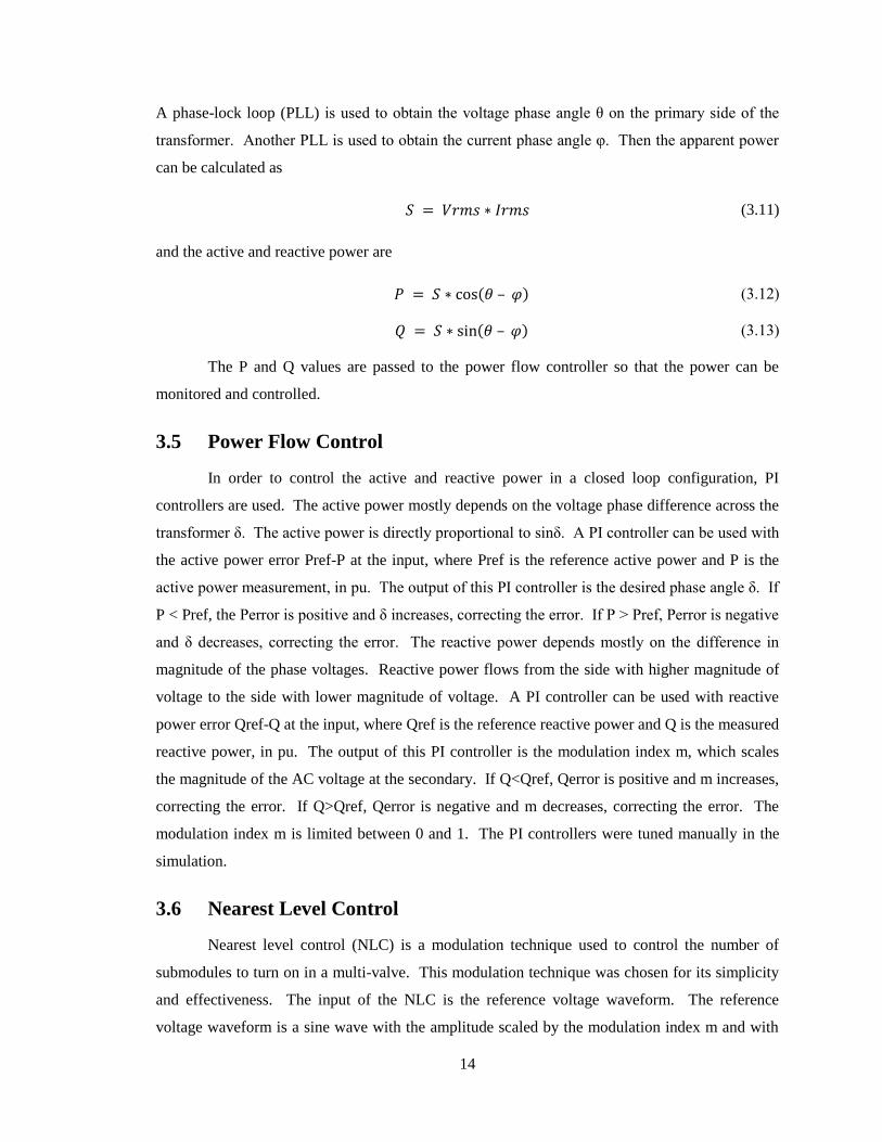
The capacitor voltages are regulated within 10±1V, meeting the specification. Figure 4-2
shows the capacitor voltage levels for a 21-level MMC.
Figure 4-2: Capacitor Voltage
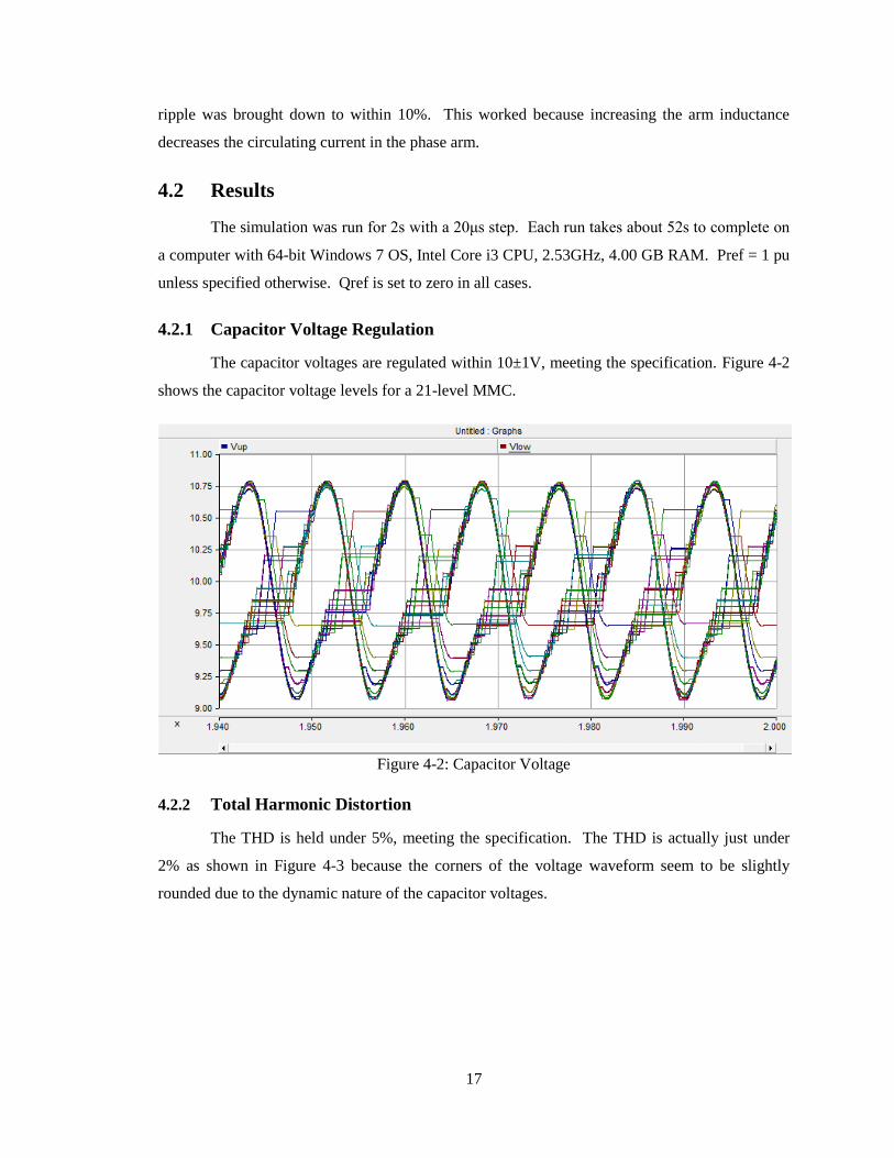
4.2.2 Total Harmonic Distortion
The THD is held under 5%, meeting the specification. The THD is actually just under
2% as shown in Figure 4-3 because the corners of the voltage waveform seem to be slightly
rounded due to the dynamic nature of the capacitor voltages.
18
Figure 4-3:AC voltage and THD
4.2.3 Power Step
The response to a 1 pu step in Pref applied at t=1s shows a rise time of about 0.1s, Figure
4-4. This corresponds to 0.1*60 = 6 cycles which is less than the specification of 10 cycles, so
the specification is met. The reactive power is not completely insensitive to the phase angle, but
it returns to zero after a short period.
19
Figure 4-4:Power Step
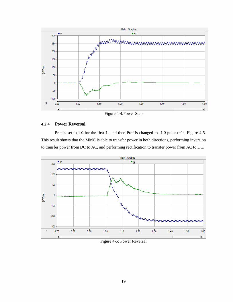
4.2.4 Power Reversal
Pref is set to 1.0 for the first 1s and then Pref is changed to -1.0 pu at t=1s, Figure 4-5.
This result shows that the MMC is able to transfer power in both directions, performing inversion
to transfer power from DC to AC, and performing rectification to transfer power from AC to DC.
Figure 4-5: Power Reversal
20
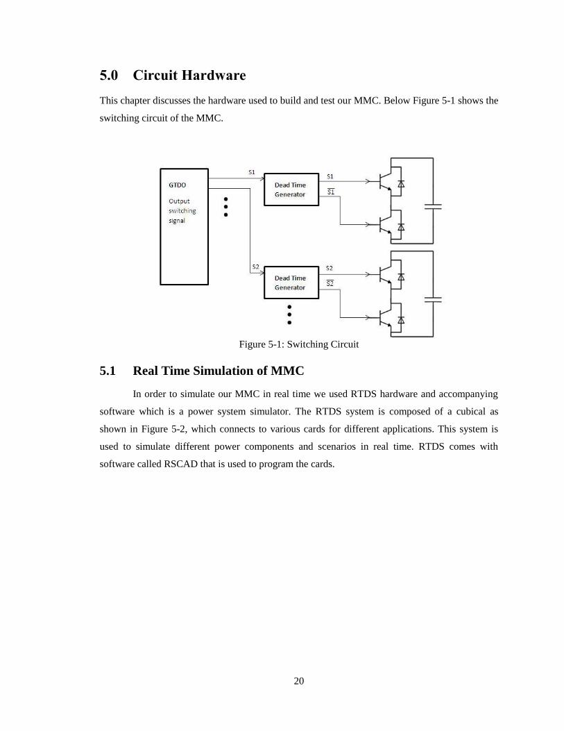
5.0 Circuit Hardware
This chapter discusses the hardware used to build and test our MMC. Below Figure 5-1 shows the
switching circuit of the MMC.
Figure 5-1: Switching Circuit
5.1 Real Time Simulation of MMC
In order to simulate our MMC in real time we used RTDS hardware and accompanying
software which is a power system simulator. The RTDS system is composed of a cubical as
shown in Figure 5-2, which connects to various cards for different applications. This system is
used to simulate different power components and scenarios in real time. RTDS comes with
software called RSCAD that is used to program the cards.
21
Figure 5-2: Portable RTDS Cubical
5.1.1 RSCAD
A five level MMC control scheme was implemented on RSCAD, with the intention of
increasing the levels later. 5 levels were used because the required measurement signals fit onto
one GTAI card. The controls are implemented in open loop for testing, with the intention of
using a closed loop system when the open loop system functions properly. The measurement
system is configured exactly as described in Chapter 3.4, with PLLs to find the voltage and
current angles, and RMS meters to find the RMS values of the voltage and current signals. The
controls consist of the reference voltage signal generator, the NLC and the BCA. For the open
loop system the control variables are m and δ. The RSCAD circuit can be found in Figure C-1, C-
2, C-3 in Appendix C.
5.1.2 RTDS Hardware
We used a RTDS portable cabinet along with two I/O cards, GTDO and GTAI, to
complete our simulation. The GTDO is a digital output card that can provide up to 64 output
22
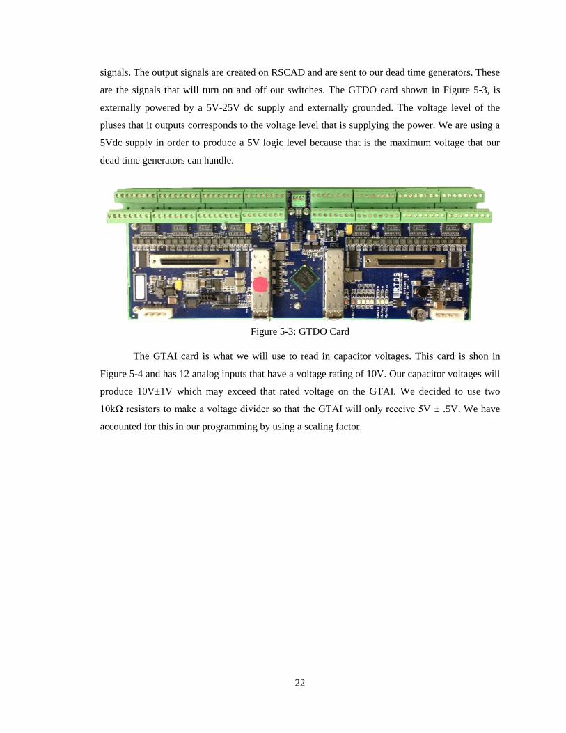
signals. The output signals are created on RSCAD and are sent to our dead time generators. These
are the signals that will turn on and off our switches. The GTDO card shown in Figure 5-3, is
externally powered by a 5V-25V dc supply and externally grounded. The voltage level of the
pluses that it outputs corresponds to the voltage level that is supplying the power. We are using a
5Vdc supply in order to produce a 5V logic level because that is the maximum voltage that our
dead time generators can handle.
Figure 5-3: GTDO Card
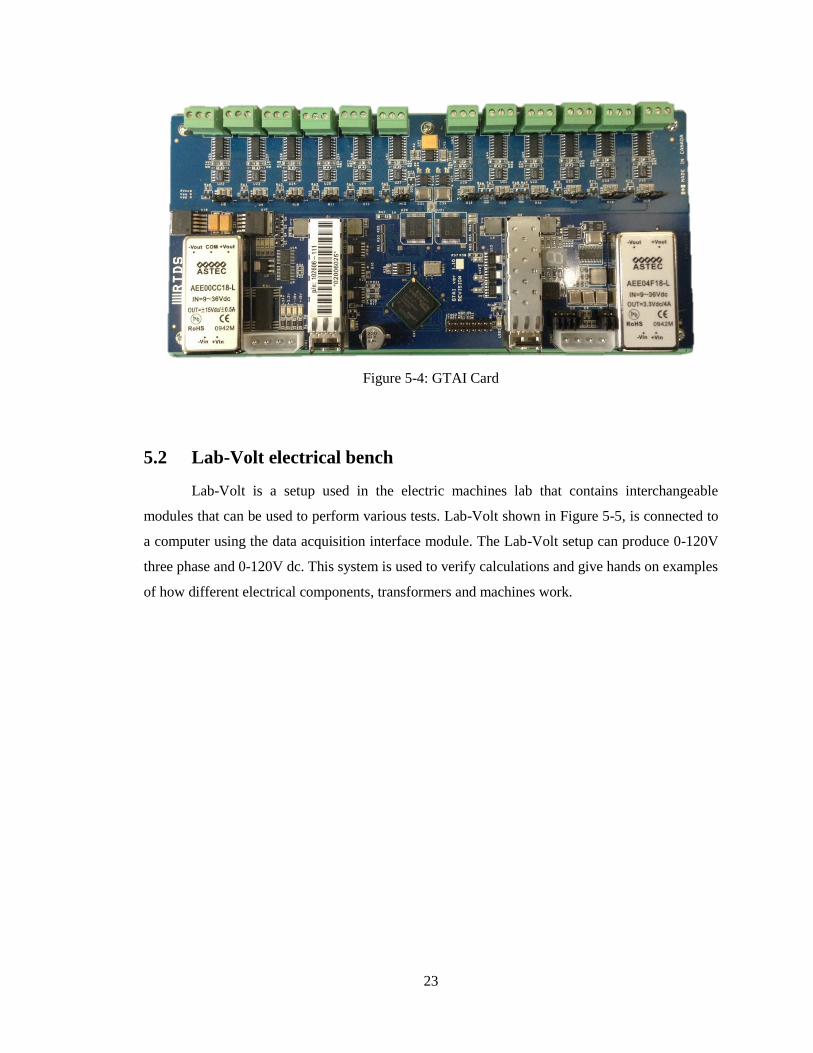
The GTAI card is what we will use to read in capacitor voltages. This card is shon in
Figure 5-4 and has 12 analog inputs that have a voltage rating of 10V. Our capacitor voltages will
produce 10V±1V which may exceed that rated voltage on the GTAI. We decided to use two
10kΩ resistors to make a voltage divider so that the GTAI will only receive 5V ± .5V. We have
accounted for this in our programming by using a scaling factor.
23
Figure 5-4: GTAI Card
5.2 Lab-Volt electrical bench
Lab-Volt is a setup used in the electric machines lab that contains interchangeable
modules that can be used to perform various tests. Lab-Volt shown in Figure 5-5, is connected to
a computer using the data acquisition interface module. The Lab-Volt setup can produce 0-120V
three phase and 0-120V dc. This system is used to verify calculations and give hands on examples
of how different electrical components, transformers and machines work.
24
Figure 5-5: Lab-Volt Setup
5.2.1 Data Acquisition Interface
During the testing and design of the MMC we used the DAI to monitor the currents in the
arms of the multi-valve as well as the input and output voltage levels. Using the DAI also gives
us an oscilloscope and multimeter with multiple inputs that we used while preforming testing on
out MMC. This information will appear to us on the same computer that we will use to control
the GTDO card. As we modified our project we ended up using the DAI only as an oscilloscope
to get the MMC waveform. We used the Lab-Volt setup instead of an actual oscilloscope because
it has higher voltage ratings.
25
5.2.2 Power supply and other components
For our MMC we required a DC voltage supply to charge our capacitors. The Lab-Volt
set up has a variable 0-120VDC supply but after testing the waveform we found that it was not
very constant. Instead we used Lab-Volts 0-120VAC supply connected to a power diode unit.
This rectified our voltage to give us a constant DC voltage. The problem we faced is that with
MMC the direction of power flow changes and the current would flow into our DC source. The
power diodes would not let the reverse current flow and so in the end we did not use the Lab-Volt
power supply or the power diode unit. During testing and building of the MMC we used four
resistor modules that each contain a 300Ω, 600Ω and 1200Ω resistor all connected in parallel to
equal 43Ω. This resistor will be plugged into our circuit connecting the two inductors to the
ground. In the end we replaced these resistors with regular resistors because we no longer
required the high power ratings on the resistors and a 1W resistor is much more mobile then
being connected to the Lab-Volt setup.
5.3 Component Selection
We decided early on in our project to build our MMC on multiple breadboards. Because
of this all of the components had to be through hole components. All of our electronic
components were ordered through the university through Digi-Key. In some cases the electrical
shop already had some of the necessary components and was able to provide us with them so we
did not have to order them. A detailed bill of material can be found in Appendix A.
5.3.1 MOSFETs
One of the main components in an MMC is the switch. The switch is what determines
which capacitor is charging and whether there is voltage across it or not. The switch we decided
to use is a power MOSFET that has a built in reverse diode. We decided to use a MOSFET
because they have less noise than a BJT and were a lot smaller than an IGBT. The main reason
for selecting a MOSFET transistor was based on price and availability. At the time of selection
and ordering, there were several MOSFETS available for a cost that met our budget. A lot of the
other types of transistors were either out of stock or we would have to contact Digi-Key for cost
details and special orders. In the end we did not end up using the MOSEFTS due to the fact that
the gate voltages were floating. The circuitry required to solve the gate voltage problem was too
large and complex for the scope of our undergraduate project.
26
5.3.2 Capacitors
The capacitors chosen for our submodules are 4.7mF with a voltage rating of 25V. The
original voltage across the capacitor was going to be 10V±1V. GTAI card is rated for 10V so we
used a resistive voltage divider to lower the voltage to 5 volts to insure that we did not exceed the
voltage rating on the GTAI card. We noticed that the capacitors discharged too quickly with the
resistive dividers so instead we decided to charge the capacitors to 9V and not use the resistive
dividers.
5.3.3 Gate Drivers
We purchased gate drivers for out MMC to input the signal from the GTDO and convert
the signal into two separate signals, one the inverse of the other. The two output signals from the
gate driver would go directly to the two transistors in a submodule to insure that the switching
happened at opposite times.
5.3.4 Dead Time Generators
After testing the above gate drivers we realized that the output of the two inverted signals
happened instantly which would cause the transistors to fail because the switches do not turn on
and off instantly. Each switch needs time to fully turn off before the other switch is turned on
otherwise we would short circuit the capacitor. In order to compensate for this we replace the gate
drivers with dead time generators. The dead time generators produce the output signal and the
inverted output signal 2µs apart from each other. This will allow enough time for the transistors
to switch without problems. The dead time generators are powered by a 5V supply and receive a
clock pulse from a 4MHz crystal oscillator.
5.3.5 Inductors
The two inductors in the arms of the multi-valves are used to help balance and control the
current flowing through the multi-valve. We have chosen 10mH inductors for this use. We also
planned on using a 3.9mH for the input of the multi-valves. This inductor acts like a 1:1
27
transformer to help control the power flow. Since we changed our project to show half the
waveform of the MMC we only needed one multi-valve and no longer needed these inductors.
5.3.6 Optocouplers
Due to the problem of floating gate voltages, we were required to find a new type of
transitory. An optocoupler consists of a photo diode that when given a current sends light to a
photo transistor which switches the transistor on. This way there is no need for isolated voltages
at the gate inputs. These optocouplers how ever did not include reverse diodes in the transistor
part which are required in the MMC configuration for the switch. We used a standard 104 diode
across the emitter and collector of the transistor. At the input of the transistor we are supplying
5V so we added a 220Ω resistor to limit the current to 17mA (equation 1) to insure that we did
not exceed the rated current of 60mA and burn any switches.
28
6.0 Testing and Simulation Reconciliation
This chapter covers the actual testing preformed on our physical components as well as
our physical MMC circuit.
6.1 Components
Before constructing our MMC we first tested the individual components that we were
going to use to make sure that they worked before inserting them into the circuit.
6.1.1 Switches
The first component that we tested was the MOSFET transistor. We connected the drain
to 5V through a 5Ω resistor and the source to ground. We then connected the gate to ground and
observed 0V across the resistor. Next we connected the gate to the 5V source and read 5V across
the resistor. This testing made sure that the transistor would turn on with a 5V gate impulse and
that the transistor would be able to handle 1A of current flowing across it. Figure 6-1 shows the
time that the MOSFET takes to turn on.
We preformed similar testing on our optocoupler to ensure that all of the switches in our
circuit would work. The optocouplers have a much lower power ratings so we had to add a 220Ω
resistor to the 5V gate pulses for the input because it is rated for 60mA. We connected the
collector to a 5V supply through a 10KΩ resistor to insure that there was a small current flowing
across the transistor. The emitter was then connected to the ground. Once we were sure that all
the optocouplers worked, we added them to the circuit.
Figure 6-1: MOSFET Switching Time
29
6.1.2 Gate Driver
When testing the gate drivers, we noticed that there was no dead time in the two signals.
The delay shown in Figure 6-2 below is the delay of the wire connecting the two inputs of the
gate driver together. Since there is no dead time, we decided to use a dead time generator instead
of these gate drivers.
Figure 6-2: Gate driver
6.1.3 Dead Time Generators
In order to ensure that the dead time generators we selected gave us a large enough gap of
the inverted signals we connected them to a 5V 60Hz signal and viewed the output waveform on
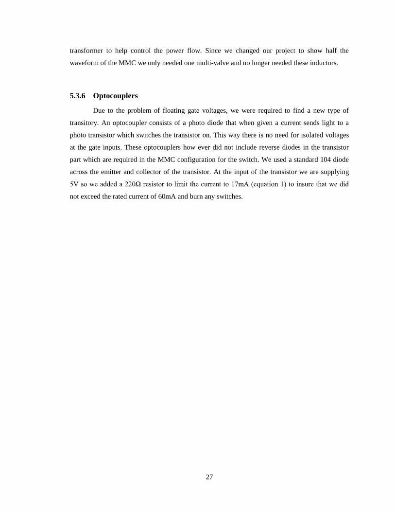
an oscilloscope. We observed 2µs of dead time as shown before in Figure 6-3, which was more
time than needed for the switches to finish switching.
30
Figure 6-3: Dead Time
6.1.4 Capacitors
The capacitors that we used held a 8-10V charge, so we thought it was necessary to test
the capacitors to make sure all of them could hold a charge for a long enough length of time
without discharging. This test was very simple as we connected one end or the capacitor across a
10V source and ground through a 50Ω resistor. We then pulled the capacitor from the circuit and
let it sit for 5 minutes and measured the voltage across the two terminals to verify the voltage
level.
6.1.5 Crystal Oscillator
When testing our circuit, we noticed that our switches we not switching properly and
since we had already tested all the switches and dead time generators we decided to test the
crystal oscillators that give the clock pulse to the dead time generators. We connected the crystal
oscillator to an oscilloscope to ensure that it was generating a 4MHz pulse, which is was.
6.2 Single Submodule
When constructing our MMC, we first built one submodule to make sure that the two
switches were operating properly and that the capacitor was keeping its charge. We used two
10kΩ resistors to build a voltage divider across the capacitor because we were supplying 10V to
the capacitor but the GTAI card had a voltage rating of 10V. The resistive divider lowered the
voltage seen at the GTAI input to 5V but also discharged our capacitor. We decided to instead
charge the capacitors to 8V so that we no longer required the resistive divider.
31
6.3 Five levels
Once we had a working submodule, we constructed a 5-level MMC which contained 4
sublevels in each multi-valve. We planned to construct the full 11-level MMC once the 5-level
MMC was working, but problems while testing the 5-level changed that. While testing the 5-level
MMC we came across switching problems where only the top submodule actually switched
correctly. After further testing and research, we realized that the gate voltages were not refenced
to ground and were floating. In addition to this, the gate voltage needed to be 5V above the source
voltage of the transistor. This is a complicated problem because the transistors are constantly
switching so the voltage level at the source is constantly changing also. The solution to this
problem was to add a floating MOS gate driver IC along with an isolated DC-DC converter. We
decided against using this solution because ordering parts needed would exceed our budget and
there was not enough time remaining to implement all of it. We decided to solve our problem by
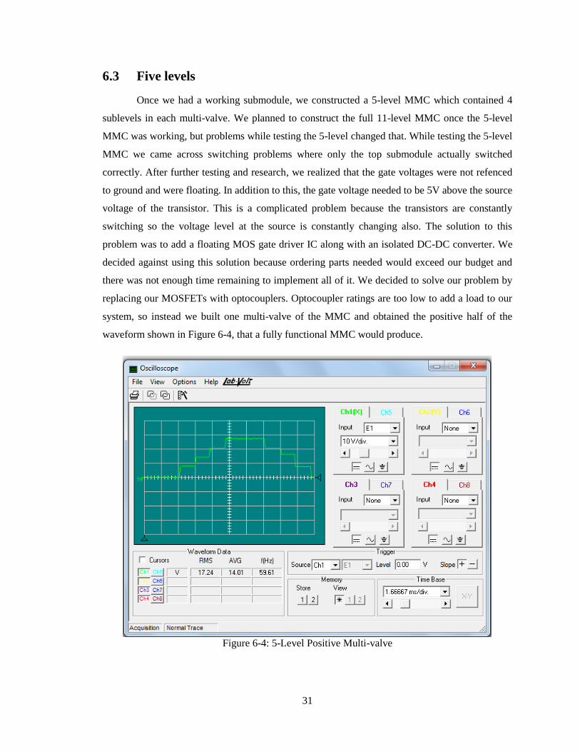
replacing our MOSFETs with optocouplers. Optocoupler ratings are too low to add a load to our
system, so instead we built one multi-valve of the MMC and obtained the positive half of the
waveform shown in Figure 6-4, that a fully functional MMC would produce.
Figure 6-4: 5-Level Positive Multi-valve
32
7.0 Future Work
This project can be continued by increasing the number of levels and by implementing
our MMC circuit in three phase. Circuit protection can also be added to this design as well as
building it on a printed circuit board.
7.1 Increase Levels
Increasing the number of levels of the MMC directly decreases the THD of the AC
voltage. It also makes it possible to increase the RMS voltage and the power rating. Adding
levels does not increase the complexity of the system by much. However, adding levels increases
the size and cost of the hardware. More submodules require more ports on the GTAI and GTDO
cards, which may require additional cards.
7.2 Three Phase
The MMC was originally designed to work in 3 phase. Several aspects of the design
would be simpler and work better in 3 phase. The measurement system would work better since
it is easier to calculate the quantities in 3 phase, most notably the active and reactive power.
Since the phase angle can be determined directly from the instantaneous signals using all 3
phases. The PLL components in PSCAD and RSCAD all have 3 phase inputs, these components
are not designed to work for single phase. Finding the RMS voltage is easier as well. The
voltage signals can be rectified and an averaging filter is used to track the RMS voltage. This
method of measuring the RMS voltage does not work as well for single phase because the
rectified signal has larger harmonics than a 3 phase rectified DC.
In order to implement the system in three phase, 3 times the components would be
required. A 21-level single phase MMC already has a lot of components. There are (21-1)*2 =
40 submodules. Each submodule has 2 switches and 1 capacitor. There are 80 switches and 40
capacitors. Each switch needs to be connected to a dead time generator. One dead time
generator can supply gate signals for 6 switches, or 3 submodules. This means that ceil(40/3) =
14 dead time generator ICs are needed. Each dead time generator requires 3 ports on a GTDO
card, one for each submodule. The number of GTDO ports required is 40, which is attainable
with a single card. The number of GTAI ports required is also 40 for capacitor voltage and 4 for
the current and voltage measurements. Each GTAI card has 12 ports so ceil(44/12) = 4 cards are
required. For 3 phase, 240 switches, 120 capacitors, 40 dead time generators, 2 GTDO cards and
33
11 GTAI cards. This is a lot of parts, most notably the GTAI cards which are not so easily
obtained.
In a 3 phase system the instantaneous power flow has a large DC component with a small
double frequency component. This power can be unidirectional, unlike single phase power that
has larger oscillations and may even change sign for a short duration. Since the power can be
unidirectional, the current from the DC voltage supply can be positive all the time, which can be
supplied by a rectified DC power supply which is readily available from the Lab-Volt setup.
7.3 Complete Hardware Implementation
In order to make the MMC function properly, a number of changes need to be made. The
connection to a DC voltage source needs to be established, and the gate drive system needs a total
redesign.
The DC voltage sources that were readily available from the Lab-Volt setup are 3 phase
rectified. This means that the current can only flow out of the positive terminal, and into the
negative terminal. For the single phase implementation it is required for the current to flow in
both directions so that the submodule capacitors can charge and discharge and the voltage can be
controlled. Using a rectified DC voltage source that capacitors can only charge and the voltage
cannot be controlled, the voltage always increases. In order to fix this problem, a three phase
system can be implemented or a DC voltage source with bidirectional current flow can be used.
This DC voltage source can be created using a VSC. The simplest VSC that can be used is a 2-
level 3-phase VSC, which is available on Lab-Volt module 8837-B in the lab. This module
consists of IGBT chopper/inverter circuit that can be configured as a 2-level 3-phase VSC and the
gate signals can be connected to the RTDS through a dead time generator. A constant DC voltage
is desired so an LC filter should be placed in the DC link. This addition creates a system like a
HVDC link, with one of the converters being an MMC and the other a 2-level VSC. The control
system now needs to control not only the active and reactive power flowing through the MMC,
but the DC voltage and reactive power at the VSC must also be controlled. The number of PI
controllers increase from 2 to 4 which makes tuning the controllers much more difficult.
The gates drive system needs to be able to supply the gate voltage Vgs with varying Vs.
It is possible to provide the gate signal to the lower transistor in a submodule by using the
capacitor voltage. To do this an optocoupler and a resistor can be connected across the capacitor.
The most difficult problem is the gate voltage Vgs on the upper transistor in each submodule.
34
The transistors are NPN so they turn on when the gate voltage is supplied. When the upper
transistor is on the voltage drop Vds is small and the drain is connected to the positive terminal of
the capacitor. The voltage Vs is approximately equal to the voltage at the positive terminal of the
capacitor. To turn on the transistor Vg needs to be greater than Vs, which means the gate voltage
Vg needs to be greater than the submodule capacitor voltage.
To implement the gate drive system, a floating MOS-gate driver IC can be used [7]. This
IC is designed to be used in 2-level applications, where the lower switch has constant Vs. In
order to make this work for the MMC, an isolated voltage source may be used on each
submodule. An isolated voltage source can be obtained from a DC-DC converter. The addition
of these components increases the cost of each submodule dramatically. With all of the
peripheral components of these ICs, the total number of components needed increases as well, so
the size of each submodule increases.
7.4 Protection
In order to protect the switches from fault or surge current which could damage them, a
bypass switch can be added. The event that is most important to protect against is a DC fault. In
a DC fault, the current flows from AC to DC. This current would flow through the diodes and
may damage them. A small thyristor can be connected with its anode connected to the lower
terminal of the submodule and the cathode connected to the upper terminal of the submodule. To
protect against AC faults another thyristor can be added in parallel to the other in the opposite
direction. Another way to protect the transistors is to use a resettable fuse in series, which would
act like a circuit breaker.
7.5 Printed Circuit Board
In order to make the MMC truly modular, a PCB design needs to be created for one
submodule, carrying everything that the submodule requires. Each board would have the two
switches with reverse diodes and a capacitor, as well as a different dead time generator with 2
outputs, a floating MOS-gate driver IC and an isolated voltage source. The MMC is then
assembled by plugging these PCBs into a backplane. This way changing the number of levels is
as simple as plugging in or pulling out these PCBs. The controls may have to be implemented in
a different way, possibly using a microcontroller with some communication to receive the gate
signals and send the capacitor voltages.
35
7.6 Circulating Current Suppressing Controller
In a 3 phase MMC there are circulating currents that flow between the phase units. These
currents can result in higher power losses. The circulating currents are caused by differences in
the phase unit voltages. In order to suppress the circulating current, the current difference in each
phase unit is calculated, the phase currents are transformed to dq coordinates and fed into PI
controllers. The output of the CCSC is a voltage difference reference signal which is then fed to
the power controller [8]. The use of a CCSC may be used to decrease power losses, but adds to
the complexity of the control system.
36
8.0 Conclusion
This report has outlined the design and implementation of a modular multilevel
converter. Through the use of a five level MMC we were able to provide the positive half
waveform of a fully functional MMC. The objectives of our project were as follows:
- Simulation of 21-level MMC
- Implementation of an 11-level MMC
We designed and simulated a 21-level MMC using PSCAD. The simulation objective was
met for 21 levels and simulation plots were produced that met our specifications.
After the simulations were completed we started selecting appropriate components that would
be used to build the 21-level MMC. At first we built 11 levels for testing purposes. After some
trouble shooting we realized that our power MOSFETS would not switch because we could not
produce the appropriate gate voltage due to the fact that the source voltage was constantly
changing. In order to complete a full MMC the solution to this problem exceeded our budget and
would take too long. We then decided to build one multi-valve using optocouplers instead of
MOSFETS. These optocouplers have low power ratings so there cannot be a load connected to
the end of the MMC. Our circuit now produces the positive half waveform that a 5-level MMC
would produce.
37
Appendix A: Bill of Material
Table A-1: Bill of Material
Part Model Number Quantity Cost
Power MOSFET NTD4960N-1GOS-
ND
25 $7.99
Power MOSFET NTD4906N-35GOS-
ND
100 $38.72
4.7mF Capacitor P5159-ND 50 $56.76
Gate Driver TC4428CPA-ND 50 $49.40
3.9mH Inductor M8384-ND 1 $7.70
10mH Inductor M8386-ND 2 $15.40
Dead Time Generator IXDP630PI 10 $43.19
Optocoupler 4N25 20 Free
10kΩ Resistor n/a 50 Free
220Ω Resistor n/a 20 Free
100kΩ Resistor n/a 1 Free
Subtotal $219.16
Tax $26.30
Total $245.46
38
Appendix B: PSCAD Design
Figure B-1: Main Schematic
Figure B-2: MMC Schematic
39
Figure B-3: Multi-valve Schematic
40
Appendix C: RSCAD Design
Figure C-1: Connections to GTAI and GTDO Cards
41
Figure C-2: Control System
42
Figure C-3: Measurement System
43
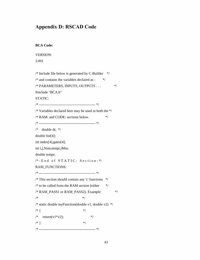
Appendix D: RSCAD Code
BCA Code:
VERSION:
3.001
/* Include file below is generated by C-Builder */
/* and contains the variables declared as - */
/* PARAMETERS, INPUTS, OUTPUTS . . . */
#include "BCA.h"
STATIC:
/* ----------------------------------------------- */
/* Variables declared here may be used in both the */
/* RAM: and CODE: sections below. */
/* ----------------------------------------------- */
/* double dt; */
double list[4];
int index[4],gates[4];
int i,j,Nsm,tempi,iMin;
double tempr;
/* - E n d o f S T A T I C : S e c t i o n - */
RAM_FUNCTIONS:
/* ----------------------------------------------- */
/* This section should contain any 'c' functions */
/* to be called from the RAM section (either */
/* RAM_PASS1 or RAM_PASS2). Example: */
/* */
/* static double myFunction(double v1, double v2) */
/* */
/* return(v1*v2); */
/* */
/* ----------------------------------------------- */
44
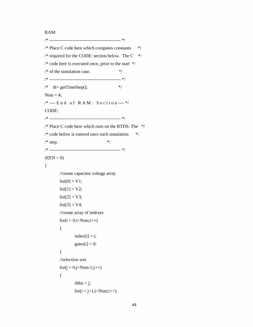
RAM:
/* ----------------------------------------------- */
/* Place C code here which computes constants */
/* required for the CODE: section below. The C */
/* code here is executed once, prior to the start */
/* of the simulation case. */
/* ----------------------------------------------- */
/* dt= getTimeStep(); */
Nsm = 4;
/* ---- E n d o f R A M : S e c t i o n ---- */
CODE:
/* ----------------------------------------------- */
/* Place C code here which runs on the RTDS. The */
/* code below is entered once each simulation */
/* step. */
/* ----------------------------------------------- */
if(EN > 0)
//create capacitor voltage array
list[0] = V1;
list[1] = V2;
list[2] = V3;
list[3] = V4;
//create array of indexes
for(i = 0;i<Nsm;i++)
index[i] = i;
gates[i] = 0;
//selection sort
for(j = 0;j<Nsm-1;j++)
iMin = j;
for(i = j+1;i<Nsm;i++)
45
if(list[i] < list[iMin])
iMin = i;
if(iMin != j)
tempr = list[j];
list[j] = list[iMin];
list[iMin] = tempr;
tempi = index[j];
index[j] = index[iMin];
index[iMin] = tempi;
//set gates
if(N > 0)
if(Imv > 0)
for(i = 0;i<N;i++)
gates[index[i]] = 1;
else
for(i = 0;i<N;i++)
gates[index[Nsm-i-1]] = 1;
Q1 = gates[0];
Q2 = gates[1];
Q3 = gates[2];
Q4 = gates[3];
/* ---- E n d o f C O D E : S e c t i o n --- */
46
NLC Code:
VERSION:
3.001
/* Include file below is generated by C-Builder */
/* and contains the variables declared as - */
/* PARAMETERS, INPUTS, OUTPUTS . . . */
#include "NLC.h"
#include <math.h>
STATIC:
/* ----------------------------------------------- */
/* Variables declared here may be used in both the */
/* RAM: and CODE: sections below. */
/* ----------------------------------------------- */
/* double dt; */
/* - E n d o f S T A T I C : S e c t i o n - */
RAM_FUNCTIONS:
/* ----------------------------------------------- */
/* This section should contain any 'c' functions */
/* to be called from the RAM section (either */
/* RAM_PASS1 or RAM_PASS2). Example: */
/* */
/* static double myFunction(double v1, double v2) */
/* */
/* return(v1*v2); */
/* */
/* ----------------------------------------------- */
RAM:
/* ----------------------------------------------- */
/* Place C code here which computes constants */
/* required for the CODE: section below. The C */
/* code here is executed once, prior to the start */
/* of the simulation case. */
/* ----------------------------------------------- */
/* dt= getTimeStep(); */
/* ---- E n d o f R A M : S e c t i o n ---- */
CODE:
47
/* ----------------------------------------------- */
/* Place C code here which runs on the RTDS. The */
/* code below is entered once each simulation */
/* step. */
/* ----------------------------------------------- */
Nn = round(Vref/Vc)+Nsm/2;
Np = Nsm - Nn;
/* ---- E n d o f C O D E : S e c t i o n --- */
48
References
[1] S. Shinde et al., “The Role of Power Electronics in Renewable Energy Systems Research
and Development,” in 2nd
Int. Conf. on Emerging Trends in Engineering and Technology,
Nagpur, Maharashtra, India, 2009 , pp. 726-730.
[2] N. Hingorani, “Future Role of Power Electronics in Power Systems,” in Proc. Of 1995
Int. Symp. on Power Semiconductor Devices & ICs, Yokohama, Japan, 1995, pp. 13-15.
[3] H. Saadat, “Basic Principles,” in Power System Analysis, 3rd
ed., PSA Publishing, 2010,
ch. 2, sec. 6, pp. 65-66.
[4] J. Peralta et al., “Detailed and Averaged Models for a 401-Level MMC-HVDC System,”
IEEE Trans. Power Del., vol. 27, no. 3, pp. 1501-1508, 2012.
[5] Q. Tu and Z. Xu, “Impact of Sampling Frequency on Harmonic Distortion for Modular
Multilevel Converter,” IEEE Trans. Power Del., vol. 26, no. 1, Jan 2011.
[6] M. Saeedifard and R. Iravani, “Dynamic Performance of a Modular Multilevel Back-to-
Back HVDC System”, IEEE Trans. Power Del., vol. 25, no. 4, Oct 2010.
[7] International Rectifier, Appl. Note 978
[8] Q. Tu et al., “Reduced Switching-Frequency Modulation and Circulating Current
Suppression for Modular Multilevel Converters,” IEEE Trans. Power Del., vol. 26, no. 3,
Jul 2011.