Developing a Controller for an Electric Motorcycle Driven by a Permanent Magnet Brushed DC Motor Group Design Project submitted in partial fulfillment of a Bachelor of Science in Electrical and Computer Engineering in the Faculty of Engineering at the University of Manitoba Group 12 Kasun Samarasekera Udeesha Annakkage Malsha Annakkage Supervisor Dr. Shaahin Filizadeh, Ph.D, P.Eng. Electrical and Computer Engineering Department University of Manitoba Technical advisor from the Power Systems Group Mr. Erwin Dirks Electrical and Computer Engineering Department University of Manitoba c Copyright 2013 Malsha, Kasun, Udeesha
Transcript
Developing a Controller for an Electric
Motorcycle Driven by a Permanent Magnet
Brushed DC Motor
Group Design Project submitted in partial fulfillment of a Bachelor of Science in
Electrical and Computer Engineering in the Faculty of Engineering at the University of
This section provides the motivation behind this design project, along with the set of objectives
and goals. Furthermore, a high level system overview is provided. This overview is intended
to enhance the understanding of the components involved in the overall project and how each
component is related one another.
1.1 Motivation
The automotive industry has become increasingly dependent on fossil fuels. The U.S Envi-
ronmental Protection Agency (EPA) states that internal combustion engines (ICE’s) produce up to
50% of ozone emissions, 90% of carbon monoxide, and 60% of air toxins found in urban areas [4].
ICEs not only deplete the world’s resources of fossil fuels but also cause multiple side effects such
as air pollution, acid rain, and global warming. Additionally, as fossil fuels become more scarce,
fuel prices increase which provides incentive to find alternative propulsion systems such as elec-
tric vehicles. Electric drive-trains are becoming increasingly popular in automotive applications
to reduce the negative environmental impact ICE vehicles. They offer higher performance than
conventional gas powered drive trains, reduce noise, and eliminate emissions. Therefore, there is
great opportunity in investigating electric vehicles, such as electric motorcycles.
1.2 Objectives and Goals
The purpose of this design project is to design and implement a controller for an electric mo-
torcycle to manage the acceleration through torque control of a permanent magnet direct current
(PMDC) brushed motor. Figure 1 illustrates the motorcycle for which the controller were designed.
13
Figure 1: Electric Motorcycle
A model for the overall system will be developed on an electromagnetic transient simulation
software upon which design decisions can be made. Following the simulation, the converter will
be implemented in hardware using power electronics. The control system will also be imple-
mented in hardware through a microcontroller which will send appropriate control signals to the
dc-dc converter. The rest of the hardware such as the batteries, motor, battery management sys-
tem (BMS), lights, display, and the motorcycle itself was purchased and is already functional. The
simulation results for entire system will set the criteria for the hardware system performance. Fur-
thermore, a drive cycle analysis to determine the power and energy requirements of the vehicle
will be performed.
1.3 Full System Diagram and High Level Overview
In this section, a high level overview will be provided which can be referenced throughout this
report to provide an overall understanding of the entire system and how all the components work
together. The system can be broken down into two components: the high power components and
the low power components, as illustrated in Figure 2.
14
Figure 2: High Level Full System Block Diagram
The primary high power components include the batteries, the dc-dc converter, and the motor.
The primary low power component is the microcontroller. The microcontroller receives inputs
from the motor current and the reference torque from the throttle and outputs a control signal to
the dc-dc converter which steps down the battery voltage to the desired voltage for the motor.
15
2 Mathematical Modeling & Computer Simulations
2.1 Overview of the Simulation
The simulation case will model various sub-systems of the entire system which will allow for
hardware design of system components. The main subsystems that will be modeled are motor,
controller, battery model, the power electronics for the buck converter, the control system, the
pre-charge circuit and the mechanical model. All of these models will be discussed in detail in the
following sections.
2.2 Motor Model
An introduction to the basics of a permanent magnet dc motor (PMDC) will be provided. Fol-
lowing this introduction, the dynamic modeling along with obtaining motor parameters are dis-
cussed. Finally, a simulation model of the motor on PSCAD/EMTDC is provided.
2.2.1 Introduction to PMDC Motors
A DC machine consists of a stator, which remains stationary, and a rotor, which spins. Wires
are looped around the rotor and are known as the armature windings. The permanent magnet
produces a magnetic field, which is experienced by the rotor.
A voltage is applied to the terminals of the armature winding, which sends a current through
the winding. The armature winding, which carries the current, experiences the stator’s magnetic
field and therefore produces a force, as shown in Equation 2.1.
F = B × IL (2.1)
In Equation 2.1, B is the magnetic field, I is the current, and L is the length of the wire. This
force is orthogonal to both the current and magnetic field. The direction of force is opposite on
both sides of the rotor, which causes the rotation of the rotor. Equation 2.2 describes the torque of
the motor as it turns. Figure 3 provides a visual explanation of Equation 2.2
T = BILcos(α) (2.2)
16
Figure 3: Permanent Magnet DC Motor
From Equation 2.2, it is clear that the torque is directly proportional to the current through the
motor; therefore, by controlling the current of the motor, the torque of the motor is also controlled.
Furthermore, Equation 2.3 relates torque to current by the constant K, where K is determined by
the mechanical parameters of the motor which is provided by the manufacturer.
T = KImotor (2.3)
It can also be shown that the internal DC voltage of a motor is proportional to K and the speed
of the motor, ωm, as shown in Equation 2.4.
Ea = Kωm (2.4)
The next section will describe how to dynamically model a PMDC motor.
2.2.2 Dynamic Modeling
Figure 4 shows a circuit model of a PMDC motor, where Va is terminal voltage, Ia is motor
current, Ea is internal voltage, Ra is motor resistance and La is motor inductance.
17
Figure 4: Circuit Model of Permanent Magnet DC Motor
A differential equation can be developed for the circuit as shown in Equation 2.5
dIadt
=1
La(V a−RaIa −Kωm) (2.5)
The motor has a mechanical subsystem represented by Equation 2.6, which links the mechani-
cal load on the shaft of the motor to the electrical system in Equation 2.5. The interpretation of the
parameters in Equation 2.6 are summarized in Table 1.
τm = τL + βωm + Jvdωmdt
(2.6)
Taking the Laplace transform of Equation 2.5 and Equation 2.6 we can develop a block diagram
of the PMDC motor as shown in Figure 5.
18
Figure 5: Block Diagram of Permanent Magnet DC Motor
2.2.3 Motor Parameters
The parameters of these equations are summarized in Table 1. These parameters for the PMDC
motor were provided by the motor manufacturer, Electric Motorsport.
Table 1: Parameters required to model the dc motor
Parameter Interpretation SI units MotEnergy PMDC MotorRa Armature Resistance ohms 0.01ohmLa Armature Inductance Henries 0.055mHJm Motor Moment of Inertia kg ·m2 0.018kgm2
K EMF constant NmA or V
rad 0.126
β Motor Viscous friction coefficient N ·m·srad negligible
Irated Rated continuous Current Amps 100A, 300A for 1 minuteVrated Rated Voltage Volt 48V
2.2.4 PSCAD model
As shown in Figure 22, the motor model used in PSCAD is a separately excited motor. PSCAD
does not have a model for a PMDC motor, but it can modeled as a separately excited motor with a
constant field winding current to represent to constant magnetic field from the permanent magnet.
All of the parameters in Table 1 were used as input parameters to the motor model in PSCAD. The
PSCAD model inputs a motor voltage and per unit speed and outputs a per unit torque. The per
unit torque will be input to a mechanical model, which will model the mechanical dynamics of the
motorcycle. The output of the mechanical model is the per unit speed back to the motor model.
2.3 Control System
The purpose of the control system is to control the actual torque of the motor to the value of the
reference torque from the throttle. First, the controller type must be determined. The controller19
will then be designed to meet a set of system requirements. Finally, the control system will be
coded onto the microcontroller for hardware implementation.
2.3.1 Controller types considered
There are multiple types of controllers used in the control system applications such as fuzzy
logic, proportion integral (PI), proportion integral derivative (PID), and lead/lag compensator’s
to name a few. Initially a fuzzy logic controller was considered; however, its design can be more
complex and time consuming to implement when compared with other controllers such as the
proportional-integral (PI) controller. For this project, a PI controller was implemented since it is
the most commonly used type of controller.
2.3.2 PI controller
PI control uses both proportional and integral control to reduce the error between an actual
value and a reference value, which are both input to the PI controller, as seen in Figure 6. For
this project, the actual value is the torque of the motor and the reference value is the torque from
the throttle. The integral component determines the integral of the error and scales this value by
a factor, Ki, while the proportion component scales the instantaneous error by a constant factor,
Kp. The output of the PI controller, which is the summation of the integral and proportion com-
ponents, produces the control signalD, which is the duty cycle of the PWM signal. A PWM of one
corresponds to a 100% duty cycle and a value of zero corresponds to a 0% duty cycle.
Figure 6: PI controller
The transfer function of the PI controller, Equation 2.7, contributes a pole and a zero. The pole
is placed at the origin while the zero is at the location defined by the ratio Ki/Kp. This ratio is
designed to produce the desired output response.
T (S) =Kp(s+ Ki
Kp)
s(2.7)
20
2.3.3 Integral Anti-Windup
As mentioned earlier, the output of the PI controller is limited between zero and one. An
additional limiter is placed on the integrator to avoid integral windup. Integral windup occurs
if the integral of the error gets too high as a positive or negative value, resulting in an output
that is limited to either its maximum or minimum value respectively. Even if the error changes
its sign from a positive to a negative value or vice versa, the system will be insensitive to any
variation in the error until the integral component is within the limits placed on the output. As
a result, the system’s response will be very slow. The additional limiter, which is placed on the
integral controller, ensures that the integral component does not exceed the output limits so that
the integral component can always be sensitive to the error.
2.3.4 Obtaining PI parameter using Simplex Optimization
PSCAD has a Simplex Optimization tool that takes in an objective function defined by the user
and then optimizes the parameters to reduce this object function.
Figure 7: Objective function and Simplex Optimization Module
For this project, it is desired to reduce the error in the torque reference and the actual torque.
Since torque and current are proportional, it is sufficient also control the current. The following
objective function, as shown in Equation 2.8, can be interpreted as the accumulation of absolute
average error from the beginning of the simulation to time t. To reduce the objective function,
Simplex Optimization will vary the proportion constant, defined as Ks in this simulation, and the
inverse of the integral constant, Ts, until the objective function is minimized.21
of =1
2
∫ t
0(Iref − IBatt)2 dt (2.8)
The P and I constants obtained from Simplex Optimizations for the per unitized controller was
Kp = 0.05 and Ki = 200.
2.3.5 Controller Requirements
Ideally, the motor torque should follow the reference torque from the throttle as closely as pos-
sible. In other words, the response of the system to a change in the torque reference should result
in a small percent overshoot, settling time, and rise time. The following criteria was determined
for the system’s response based on simulation results from PSCAD, in Section 2.8.1:
• Percent overshoot ≤ 40%
• Settling time ≤ 20ms
• Rise time ≤ 1.9ms
This criteria is based the condition that the system is under loaded conditions.
2.3.6 System Model
It is important to determine a transfer function for the motor and mechanical model if a more
analytical approach, such as root locus analysis, to determining the Kp and Ki constants were
to be implemented. It should be noted that the parameter values from root locus is not used in
the hardware for this project, but the technique is presented to demonstrate a detailed analytical
approach which provides the designer more control of the system’s response characteristics. The
entire system, which includes the batteries, converters, motor, and controller, can be modeled into
one system block diagram as seen in Figure 8.
It is desirable to model the system as a linear second order system to simplify the analysis of
the P and I constants.
A model for the motor and the mechanical system were simulated on PSCAD software, as seen
in Figure 9. A sinusoidal waveform was input to the motor over a range of frequencies from
0.0005Hz to 10Hz. The input sinusoid was then compared to the output sinusoid to determine the
gain and the phase shift. The results were then plotted onto a bode plot, as seen in Figure 10, from
which the characteristic of the system could be analyzed.
22
Figure 8: The entire system block diagram. Point A: Control Signal from Controller. Point B:Voltage at motor terminals. Point C: Motor current. Point D: Motor torque
Figure 9: System model
23
Figure 10: Bode plot of system
From the bode plot which was experimentally generated from the system, a few initial obser-
vations were made. First, the system initially has a 20dB/decade slope with a 90 degree phase
which corresponds to a zero at the origin; However, this slope does not cross the 0dB point at 1
rad/second indicating that there is a gain to the system’s transfer function. This gain was found
by determining that the gain crossover frequency at 2x10E-3 rad/second is about 55dB higher than
it should be if a gain was not present. The gain of the system was found to be 562.341.
The next observation from the experimentally derived bode plot in Figure 10 is that for higher
frequencies the slope becomes -20dB/decade. It is observed that there is a high peak in the tran-
sition from 20dB/decade to -20dB/decade of the magnitude plot. Additionally, the phase plot
indicates that the phase drops by 180 degrees from 90 degrees to -90 degrees at the corner fre-
quency. These magnitude and phase characteristics are of complex conjugate poles as seen in
Equation 2.9.
TF =1
1 + 2ζsωnk
+ s2
ω2nk
(2.9)
In equation 2.9, the term TF is the transfer function a system with complex poles, ζ is the24
dampling coefficient, and the term ωnk is the corner frequency. The peak of the transition, Mp, is
approximately 8dB. This corresponds to an Mp value of 2.51189. When solving for the damping
coefficient, there were two solutions as seen in equation 2.11. From the bode plot experimentally
obtained through PSCAD simulations, it is clear that the system is underdamped which corre-
sponds to a ζ value less than 0.707; Therefore, the ζ value of 0.203299 was chosen.
Mp =1
2ζ√
1− ζ2(2.10)
ζ = 0.203299, or0.979117 (2.11)
From the bode plot, the resonant frequency at which the peak of the magnitude plot occurs
was found to be at 0.075Hz. Using Equation 2.12, the corner frequency can be calculated.
ωr = ωnk√
1− ζ2 (2.12)
ωnk = 0.492013rad/second (2.13)
Plugging the values for the damping coefficient, ζ, and the corner frequency, ωnk, into Equation
2.9 gives the transfer function for the complex poles. Combining the transfer function for the com-
plex poles with the gain and the zero at the origin as discussed earlier, the total transfer function
modeled for the system is found, as seen in Equation 2.14. The bode plot of the system model, as
seen in Figure 11, is a good approximation of the actual system whose bode plot is seen in Figure
10.
T (s) =562.341s
1 + 5.4213s+ 177.778s2(2.14)
25
Figure 11: Bode plot of system model
2.3.7 Selection of P and I constants using Root Locus Analysis
Root locus provides an analytical approach to determining the Kp and Ki constant of a PI
controller. Knowing the poles and zeros of a system provide information on how the system will
respond to a given input. Analysis of the second order system using Equations 2.15, 2.16, and 2.17
can be used to determine the systems response characteristics.
PO = 100 ∗ e−ζπ√1−ζ2 (2.15)
Ts =4
ωn(2.16)
Tr =1
ωn√
1− ζ2(πtan−1(
√1− ζ2ζ
)) (2.17)
Setting the percent overshoot equal to 43% results in a damping coefficient, ζ, of 0.259. The
damping coefficient is determined from Equation 2.15. Since the system is a linear second order
26
system with complex poles, the roots of the system are provided in Equation 2.18. The positive
angle from negative real axis to the complex roots can be easily found through Equation 2.19. For
poles of the closed loop transfer function that lie this region, the system will satisfy the percent
overshoot requirement.
s = −ζωn ±√
(ζωn)2 − (ωn)2 (2.18)
Angle = tan−1(
√1− ζ2ζ
) (2.19)
From the settling time criteria of 20.1ms, a resonant frequency, ωn, of 191.388 was found from
Equation 2.16; however, this frequency resulted in a rise time of 9.918ms, as calculated from Equa-
tion 2.17. Hence, a resonant frequency of 1200Hz was chosen resulting in a rise time and settling
time of 1.58ms and 3.33ms respectively, which both meet the system criteria.
From the root locus plot seen in Figure 12, a Kp value of 40 was chosen and Ki = 14000. The
per-unitized values with a base of 300 are 0.1333 and 46.667 for Kp and Ki respectively.
Figure 12: Root locus plot
27
The closed loop transfer function with the PI controller is seen in Equation 2.20.
Figure 16: Experimental results and fitted curves for Cd and OCV as functions of SOC
32
Figure 17: Experimental results and fitted curves for Rs and Rs as functions of SOC
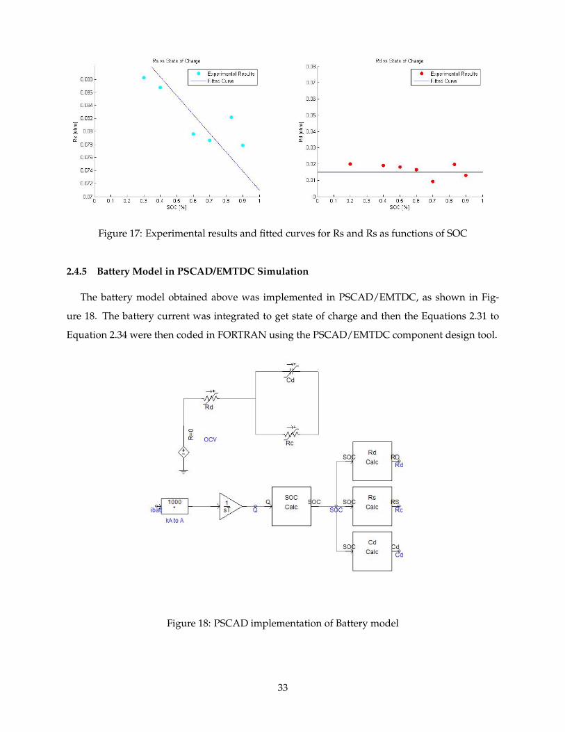
2.4.5 Battery Model in PSCAD/EMTDC Simulation
The battery model obtained above was implemented in PSCAD/EMTDC, as shown in Fig-
ure 18. The battery current was integrated to get state of charge and then the Equations 2.31 to
Equation 2.34 were then coded in FORTRAN using the PSCAD/EMTDC component design tool.
Figure 18: PSCAD implementation of Battery model
33
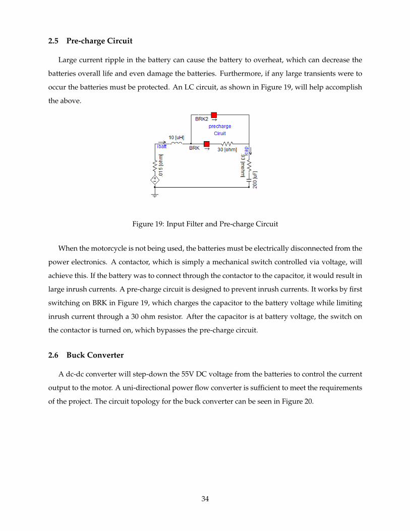
2.5 Pre-charge Circuit
Large current ripple in the battery can cause the battery to overheat, which can decrease the
batteries overall life and even damage the batteries. Furthermore, if any large transients were to
occur the batteries must be protected. An LC circuit, as shown in Figure 19, will help accomplish
the above.
Figure 19: Input Filter and Pre-charge Circuit
When the motorcycle is not being used, the batteries must be electrically disconnected from the
power electronics. A contactor, which is simply a mechanical switch controlled via voltage, will
achieve this. If the battery was to connect through the contactor to the capacitor, it would result in
large inrush currents. A pre-charge circuit is designed to prevent inrush currents. It works by first
switching on BRK in Figure 19, which charges the capacitor to the battery voltage while limiting
inrush current through a 30 ohm resistor. After the capacitor is at battery voltage, the switch on
the contactor is turned on, which bypasses the pre-charge circuit.
2.6 Buck Converter
A dc-dc converter will step-down the 55V DC voltage from the batteries to control the current
output to the motor. A uni-directional power flow converter is sufficient to meet the requirements
of the project. The circuit topology for the buck converter can be seen in Figure 20.
34
Figure 20: dc-dc Buck Converter
The MOSFETs will be controlled with a pulse width modulation (PWM) signal from the micro-
controller. The duty cycle, which is the fraction of the period in which the pulse is high, determines
the voltage that will be at the output. The relationship between the duty cycle and the output volt-
age is shown in Equation 2.35 where V o is the output voltage, D is the duty cycle and V in is the
input voltage from the battery.
V o = D ∗ V in (2.35)
An LC filter is placed at the input of the buck converter so that the input voltage and battery
current is smoothed. The presence of the capacitor will cause inrush currents if the contactor
directly applied 55V to the input capacitor. A pre-charge circuit will charge the capacitor before
the contactor is closed. Another addition was to have three MOSFETs in place of one because
the the motor can draw up to 300 A and each MOSFET is only rated 220A. The modified buck
converter design can be seen in Figure 21.
Figure 21: Modified Buck Converter
2.6.1 Buck Converter on PSCAD/EMTDC
The components of a buck converter are MOSFETs, diodes, and passive components. The MOS-
FETs and diodes behave as ideal components, so they do not incorporate the non-linear behavior
and parasitic inductances and capacitances associated with the MOSFETs and diodes. Figure 2235
shows the battery model in PSCAD/EMTDC connected to the LC input filter with the pre-charge
circuit followed by the buck converter which controls the voltage at the motor. The motor model
will be discussed in detail next.
Figure 22: Input Filter,Pre-charge Circuit, Buck Converter and Motor
2.7 Mechanical Model
In order to properly dynamically simulate the dc-drive on PSCAD/EMTDC, a proper mechan-
ical model must be developed in order to determine the load torque acting on the motorcycle. The
major forces acting on the motorcycle is the force of rolling resistance, the aerodynamic drag force,
and the force due to the inclination on the road.
2.7.1 Assumptions
The following assumptions were made for the mechanical model:
• The weight of the motorcycle is distributed evenly on the wheels.
• The lean of the motorcycle will not be a factor in the forces acting on the motorcycle.
2.7.2 Dynamic Motorcycle Model
The mechanical system can be modeled by Equation 2.6. The term τL is the load torque trans-
lated onto the wheels caused by the sum of all the total forces acting on the motorcycle, as shown
in Figure 23.
36
Figure 23: The total forces acting on the motorycle
The Aerodynamic Force: Fad
As the motorcycle accelerates to a velocity, the air on the frontal surface of the rider and motorcycle
will exert a force Fad as shown in Equation 2.36. The term ρ represents the density of air, Cd is the
drag coefficient, Af is the frontal area of the rider and motorcycle and v2v is the velocity.
Fad =1
2ρCdAfV
2v (2.36)
Rolling Resistance on an Incline: Fr
Rolling Resistance is the forces that brings a rolling wheel to an halt. This force depends on the
size of the tires and tire pressure. The constant Crr accounts for these factors. The term Mer is the
mass of the motorcycle , g is acceleration of gravity and θ is the slope of the incline.
Froll = MtotgCrrcos(θ) (2.37)
Force due to grade: Fn
As the motorcycle moves up an inclination the motor must produce more torque to prevent the
motorcycle form rolling down the hill. This force due to grade is shown in Equation 2.39 multi-
plied by sin(θ), where θ is the slope of the inclination.
Fgr = Mtotgsin(θ) (2.38)
Force of Linear Acceleration: Fla
In order for the vehicle to accelerate, a force must be applied as shown in Equation 2.39.
Fla = Mtota) (2.39)37
Force of Angular Acceleration: Fω
A rotational force must be applied in order to make the motor spin faster. Before deriving the
formula, a closer look at the rotating parts of the motorcycle is taken, as shown in Figure 24. By
intuition, as a smaller gear turns a larger gear, its speed is proportional to the inverse ratio of the
radii of the gears, as in Equation 2.40. This ratio represents the gear ratio G, where rm and rw are
the radii of the motor and wheel gears.
ωmωw
=rwrm
= G (2.40)
The torque is inversely proportional, as seen in Equation 2.41, where τe is motor torque and τl
is load torque at the rear wheel.
τeτl
=rwrm
= G (2.41)
Figure 24: The ratio of wheel radius to motor shaft radius
From Figure 24 and using the gear ratio of the wheels, the following equations can be derived.
ωw =v
rωm =
Gv
r(2.42)
Taking the derivative of the above equations results in equations:
dωmdt
=G
R
dv
dtτ =
G
RJdωmdt
(2.43)
38
Using equations in 2.43 we can derive equation2.44.
Fω = JG2
r2dv
dt(2.44)
The total tractive effort requires:
Fte = Fad + Froll + Fgr + Fla + Fω (2.45)
G
Rτe = µrrmg +
1
2ρACdv
2 +mgsin(φ) +mdv
dt+ J
G2
r2dv
dt(2.46)
Equation 2.46 represents a simple first order equation which can be easily simulated on a math
software such as Matlab or PSCAD.
2.7.3 Values used in Simulation
Table 2 summarizes all the parameters used in the overall simulation. Please note that the
parameter AfCd was not measured but approximated using a frontal area of approximately 1 and
a coefficient of drag of 0.6 [18].
Table 2: Simulation Specifications
Symbol value
Af Cd 0.6[m2]mtot 200[kg]µrr 0.002ρ 1.25 [kg/m3]r 0.2959 mΩ
G 4.3Ra 0.01 [Ω]La 0.055 [mH]β 0
Kemf 0.126Jv 0.0185 [kg/m2]
2.7.4 PSCAD Implementation
Using PSCAD component wizard and FORTRAN code the mechanical model was implemented.
Figure 25 shows the block diagram representing the differential Equation 2.46. The module inputs
the torque output from the motor and outputs per unit speed back to the motor.
39
Figure 25: Mechanical Model to left and Module to right
40
2.8 Overall Results of Simulation
2.8.1 Response to Torque Steps
Figure 26: In order from top to bottom: Motor voltage vs. time, Reference current and motorcurrent vs. time, speed vs. time, and battery current and battery voltage vs. time
Figure 26 summarizes the important response of the simulation due to torque steps. The top
graphs shows the voltage across the terminal across the motor. It has a voltage ripple of 10V which
is acceptable for our purposes. The third graph shows the speed of the motorcycle in km/hr and
the fourth shows the input capacitor voltage an battery current. The battery current ripple is 15A
41
which is 5% of 300A out maximum current.
The second graph shows the per unit motor current in response to a the current reference given.
A close up of the step response from Figure 26 is shown in Figure 27. The percent overshoot is
43%, the rise time is 1.9ms and the settling time is 20.9ms.
Figure 27: Response to 1 pu current reference
2.8.2 Maximum acceleration to reach maximum speed
Figure 28 shows the maximum current 300A being applied to the motor to get the peak torque
of the motor of 37.8 Nm. Even though the battery can output much more current, the torque is
limited by the motor. The maximum speed reached by the motor is 95 km/hr. It reaches 60 km/hr
in 7 seconds. At 11 seconds the motor reaches it rated speed and the torque begins to drop.
42
Figure 28: Response to 1 pu current reference accelerating to maximum speed
2.8.3 Drive Cycle Analysis
Drive cycle analysis is necessary to determine the range of the motorcycle. There are many
drive cycles that are available for different types of vehicles to simulate a range of driving condi-
tions, such as city driving, highway driving or aggressive driving. The simulation repeats each
drive cycle until the battery SOC has reduced from 1 to 0.1, which in other words is 10% of the
initial charge, to determine the range of the battery.
Choosing a drive cycle
A drive cycle must be chosen to simulate driving for light vehicles like the motorcycle, and also for
Manitoban city driving since that is where the motorcycle for this project is intended to be driven.
The simulation was performed on the commonly used drive cycle, ECE 15, see Figure 29, which
was based on some sample code [10]. The cycle is used for testing small electric vehicles and used
to simulate city driving conditions due to low vehicle speeds, low engine load and low exhaust
gas temperature [10]. Other cycles that can be suitable for testing are the UDDS drive cycle which
is good for city driving and used for light duty vehicle testing and the NEDC cycle which has four
ECE-15 cycles in series with a EUDC cycle which is a more aggressive drive cycle to show more
variation in the type of driving.
43
Figure 29: ECE 15 Drive Cycle
ECE 15 drive cycle simulation
The simulation for the ECE 15 drive cycle in Figure 29. A simulation flowchart, Figure [10], along
with some sample code were provided in [29]. Some algorithms needed to be changed from the
sample code to suit the conditions of the project. The algorithm to find the SOC of a Lithium
Ion battery determined using the results from the battery model tests that were conducted. The
coulomb counting technique and the SOC calculation discussed in the Battery Modeling section
2.4 were used in place of using Peukerts equation to predict the SOC of a battery. The discussion
in [3] explains that Peukert’s equation is designed for Lead-acid batteries and is used by approx-
imating constant current and constant temperature; however, when using Lithium-Ion batteries
the battery temperature is not constant; it rises due to high current discharge. The increase in tem-
perature causes an increase in the SOC, so Peukerts equations would actually underestimate the
SOC of the battery [3]. To determine the full range of the motorcycle the drive cycle was repeated
until the SOC was less than 0.1, which means that 90% of the battery charge was drained. The
following equations are needed for the calculations in the simulation.
Following the flowchart in Figure [?], the first step is to calculate the acceleration based on the
velocity data from the ECE 15 drive cycle. The Fte calculation uses the Equation 2.45. Pte, which
is the power from the gear system to the wheels of the motorcycle, can be determined from the
following equation,
Pte = Ftev (2.47)44
The power output from the motor will be increased if the motorcycle is being driven and decreased
if the motor is being used to slow down the vehicle. This is shown in the equations below, where
ηg is the gear system efficiency.
Pmotout = Pte/ηg (2.48)
Pmotout = Pteηg (2.49)
Once we know the output power from the motor, the torque can be calculated.
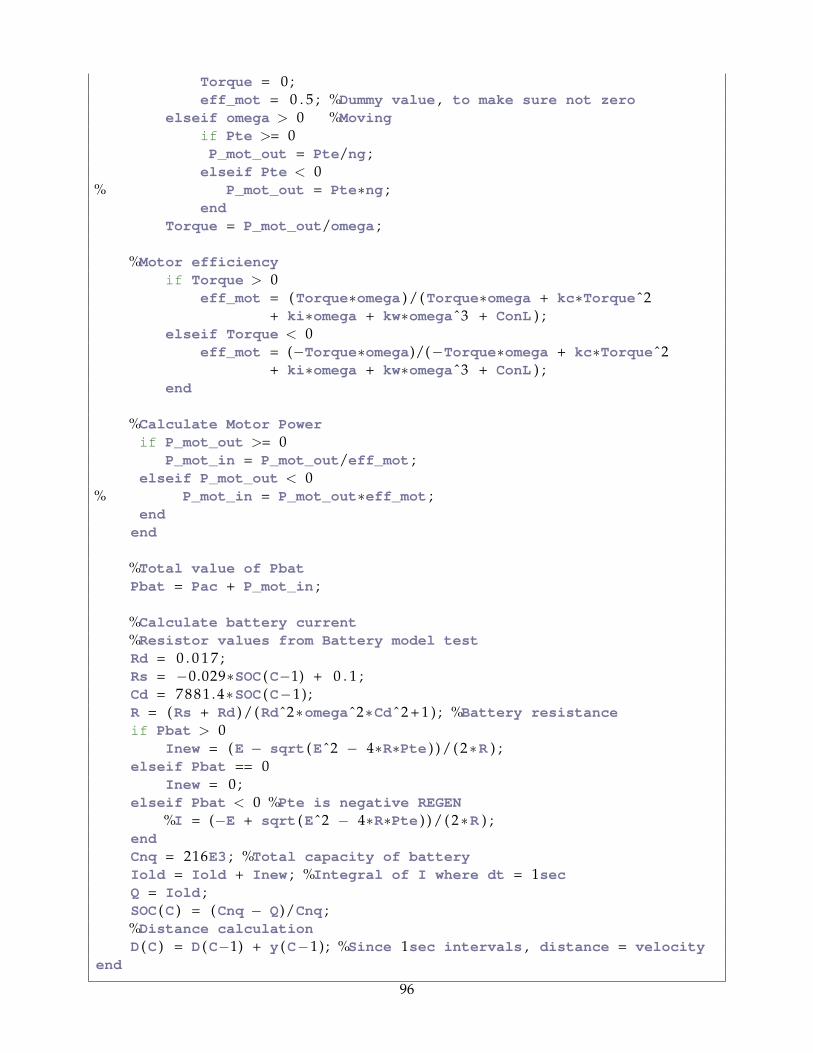
Torque = Pmotorout/ω (2.50)
The motor efficiency can be calculated with the following equation where kc is the copper loss
coefficient, ki is the iron losses coefficient, kw is the windage loss coefficient and C is the constant
The power that the motor sees from the battery can be calculated once the output power from the
motor and the motor efficiency are determined.
Pmotin = Pmotorout/(motorefficiency) (2.52)
The total power from the battery is the addition of motor input power and the accessory power.
The SOC can be calculated using the Equations 2.22 and 2.34.
45
Figure 30: State of Charge
Figure 31: State of Charge
The results from the simulation for the motorcycle range are shown in Figure 30. The voltage
discharge curve can be shown in Figure 31It can be seen that the range of the motorcycle is 201km
or 125 miles. This value is not reasonable because according to Electricmotorsport the range of the
46
motorcycle should be around 40 to 50 miles.
47
3 Hardware Implementation
In this section, the hardware used to implement the motor controller and power converter will
be discussed.
Figure 32: Full System Block Diagram
The system has two major sections: the high power components and the low power compo-
48
nents, as shown in Figure 32. The high power components include the batteries, motor and buck
converter. The low power components include the microcontroller, gate driver, current sensor, low
pass filters and PCB. Each of these components will be discussed in further detail in the following
section.
3.1 Batteries, converter and motor
The voltage of the 55V rated lithium polymer batteries are stepped down by the dc-dc buck
converter to the voltage required by the motor in order for the motor’s torque to follow the ref-
erence torque from the throttle. The motor is rated for 100A of current; however, 300A at a rated
torque of 37.8Nm can be applied for one minute. To allow for operation at 300A, three MOSFETs
in parallel are required so that the current through each MOSFET does not exceed its rated value
of 220A.
3.2 Pre-charge circuit
The pre-charge circuit, which is placed between the batteries and the input capacitor of the
buck converter, is designed to reduce inrush currents.
3.3 LC Filters
Two LC filters are used for the high power components. One is placed across the batteries and
the other is placed across the load to smooth the current and voltage waveforms. The input capac-
itor chosen for the input capacitor was a Unilytic UL3Q207K 200uF capacitor. For our application,
a thin film capacitor was chosen mainly due to the high current requirements. Electrolytic capaci-
tors have small current ripple ratings and would not be able to handle the current ripple predicted
by simulation. The output filter capacitor is an AVX 100uF polypropylene film capacitor, which
has similar ratings the UL3 and was chosen for the same reasons.
3.4 Contactor
The contactor mechanically disconnects the converter through a magnetically controlled switch.
The contactor works by magnetically pushing a copper bar which then electrically connects S1 and
S2. The contactor connects S1 and S2 when a input voltage of 48V is applied. When the key igni-
tion turns on, 48V is applied to the contactor and the battery is now electrically connected to the
converter. When the ignition turns off, the contactor disconnects S1 and S2.
49
Further details of the hardware components, along with images of the hardware, are provided
in Appendix E.
The next section will discuss the low power components. The main low power component is
the microcontroller, which is programmed to run the control system. The inputs to the microcon-
troller are the current readings from the current sensor and the torque reference from the throttle.
These inputs are first passed through low pass filters, which filter out any noise. The gate drivers,
which steps up the voltage and isolates the grounds of the PWM signal, are used for switching
the MOSFETs in the dc-dc converter. Please note that the BMS, display and lights already work-
ing components and were not designed in this project. Other components which are low power
include the regulators required for the 3.3V, 5V and 12V voltage buses.
3.5 Microcontroller
The main task of the microcontroller is to read current and torque inputs from the motor and
throttle respectively. Since the torque is proportional to the current, the throttle reference is es-
sentially a current reference. The microcontroller will then output the necessary PWM signal to
match the motor current to the throttle current reference. The microcontroller is also responsible
for sending control signals to the switches involved in the precharge circuit.
3.5.1 Required Peripherals
When choosing a microcontroller, specific features and requirements were determined in order
to choose a microcontroller that is most suitable for the application. The required peripherals
include:
• Two analog to digital converters (ADC) for the current and torque inputs
• One pulse width modulated (PWM) output channel
• A 32-bit processor to provide more than enough memory space required for the PI controller
code
Other factors to consider are whether to use fixed point or floating point for calculations. The
major difference between fixed point and floating point is that fixed point requires more code to
perform the same calculations as floating point which affects processor speed. It was determined
that since current of the motor is not quick to change in terms of processor speed, the speed of the
processor is not an issue; therefore fixed point was chosen.
50
3.5.2 Cost and board selection
Two developers were considered development platforms were considered: Texas Instruments
and Microchip. In general, Texas Instruments development boards were too expensive for the
$300 budget of this project. Overall, the price was much less for Microchip development boards
compared with Texas Instrument developments for the same set of requirements. Additionally,
Microchip has an MPLAB compile which each team member has had a lot of experience using.
The microcontroller that was chosen was the Mircochip’s Cerebot Mx7ck as shown in Figure
33, due to the reasonable price of $99, meets all the requirements, and all members of the group
has experience coding on Microchip products.
Figure 33: Microcontroller: Cerebot Mx7cK [11]
3.5.3 Coding the PI controller
The inputs to the PI controller is the actual torque and the reference torque. The system was
designed so that a 3.3V analog voltage corresponds to the maximum torque input of 37Nm (or
300A current). These inputs are passed through an analog to digital converter which outputs
a digital signal ranging from 0 to 1024. The relationship between analog and digital values is
provided in Equation 3.1.
Digital =1024
3.3∗ Vanalog (3.1)
When coding the PI controller, it is important to note that no decimal values can be used. To
increase the accuracy of calculations, the inputs were scaled so that the maximum torque input
corresponds to the maximum signed long value, as seen in Equation 3.2. Signed values, instead of
51
unsigned, were used since the error between the reference and the actual torque can be a negative
number. Figure 34 shows how each section of the PI controller was scaled.
Maximum Signed Long Number = 231 − 1 (3.2)
To ensure that the input is limited between zero and the maximum signed long number, a
limiter is placed on both inputs. In Figure 34, the term in the limiter labeled A is equal to 0,
and the term labeled B refers to the value 2097151. A simple calculation shows that 1024 scaled
by 2097151 is equal to the maximum signed long value. The output of the PI controller, which
corresponds to the period of the duty cycle, is then scaled down and limited to range between
zero and the value in the PR2 register to avoid integral windup. The value of PR2 resistor sets the
period of switching.
Figure 34: Scaled PI controller. A = 0, B = 2097151, C = 214748360
3.5.4 Overview of Code
The microcontroller is used to send control signals to the precharge and contactor switches,
along with sending the PWM signal to the DC-DC converter. Figure 35 shows a flow chart of the
entire code. See Appendix A for the actual C code. Note the ADC, PWM, initializations, system
initializations were taken or modified from sample code [12] [11].
52
Figure 35: Flow Chart of Code
53
3.6 Gate Driver Design
In order to switch a MOSFET on and off, a voltage across the gate and source, Vgs, must be
greater than a certain threshold ,Vth. The MOSFET requires a Vth greater than 3V in order to turn
on. The micro-controller outputs a maximum voltage of 3.3V; however, it is not guaranteed that
this will turn on the MOSFET. It is good practice to have Vgs much greater than the threshold
voltage to ensure turn on.
A second concern is the intrinsic parasitic capacitances; the gateCgs andCgd as shown in Figure
36. In order to switch a MOSFET on a certain amount of charge, Qg must be deposited on to Cgs
and Cgd. To turn a MOSFET off, the charge Qg, must be removed from Cgs and Cgd [13]. The time
required to charge the parasitic capacitances is directly proportional to the time required to switch
a MOSFET. The longer this switching time, the more losses that will be accumulated. To decrease
the switching time and switching losses, a large gate current is required. The microcontroller can
only source 25mA of current which will result in large switching times; therefore, a gate drive
must be able to provide this current capability.
The third desirable characteristic is electrical isolation from the high power dc-dc converter
and the low power microcontroller and control system. The gate drive solves this issue using
photodiodes to provide optical isolation in order to electrically separate the control signals. To
summarize, the gate driver must satisfy three criteria.
1. Step up the input PWM control signal from 0-3.3V to 0-12V signal.
2. Provide enough current to switch the MOSFETs fast enough at 10KhZ frequency.
3. Provide electrical isolation from the input control signal and the output control signal
Figure 36: MOSFET with intrinsic parasitic capacitances [13]
54
3.6.1 Part Selection
The part chosen for our design was the HCPL-3180 and the chip diagram is shown in Figure
39. It’s features include [7]:
• 2.5A maximum output current and 2.0A minimum output current.
• 250Khz maximum switching frequency.
• Output voltage ranges from 10V to 20V
• Has a built in optocoupler that provides optical isolation from input and output
• Is suitable for driving power MOSFETs used in high performance motor control applications
3.6.2 Gate Voltage vs Gate Charge Curves
In order to design the gate driver, it is important to understand gate voltage vs gate charge
curve as shown in Figure 37. To turn a MOSFET on, a certain amount of charge must be stored at
the gate, lets call this charge, Qg. In Figure 37, the charge Qg can be split into two sections. Section
one is represented from t0 to t2 and section two is t2 to t3. Section one represents the charge, Qgs,
stored on the Cgs. Section two represents the charge ,Qgd, stored on Cgd. Qg represents the sum of
Qgd and Qgs. At time, t3, the charge Qg has been stored and Cgs and Cgd is now fully charged and
the MOSFET is turned on, after t3 it just represents and excess charge stored on Cgs and Cgd it is
irrelevant with respect to the gate drive design.
55
Figure 37: The gate charge curve and the drain voltage and drain current vs time [13]
In order to understand the importance of the gate drive design, a closer look at how the drain
voltage and drain current waveforms as Cgs and Cgd are getting charged will be taken. From t0 to
t1 Vgs is less than Vth and the MOSFET is off, i.e no current flows. From t1 to t2, the drain current
begins to rise while the drain voltage stays constant. From t2 to t3 Cgd is being charged and the
drain voltage begins to drop until the drain voltage reaches zero. At this point, Cgd and Cgs are
fully charged and the MOSFET is now on on. From t3 onwards, excess charge is being deposited
on Cgd and Cgs. During t1 and t3, the drain voltage and the drain current are non-zero and hence
it represents the switching losses. It is highly desirable to reduce the time t3 - t1 in order to reduce
switching losses. This can be achieved by providing a large gate current to store the charge Cgd
and Cgs much faster thus reducing t3 -t1.
3.6.3 HCPL-3180 Gate Charge Curve Design for IXFN230N20T
Figure 38 shows gate charge verses Vgs of the IXFN230N20T power MOSFET. From the figure,
it is clear that a charge of 220nC is required to turn on the MOSFET.
56
Figure 38: The gate charge curve of the IXFN230N20T data sheet [8]
The current represents coulombs per second so the relation can be derived between Qg, Ig and
Tswitch which represent the total charge required to turn on the MOSFET, the gate current, and the
time to switch on the MOSFET respectively. Tswitch is also the same as t3-t1 in Figure 37.
Qgs = IgTswitch (3.3)
So if the HCPL-3180 outputs a maximum of 2.0A and our design uses three MOSFETs in paral-
lel, so that the gate current supplied to each MOSFET is 2/3 =0.6667A. So using Equation 3.3 with
Qg = 220nC and Ig = 0.6667A, Tswitch becomes 329 nanoseconds. If we are switching at 50Khz with
a period of 0.02ms the Tswitch is 300 times larger than the period.
57
Figure 39: The HCPL-3180 Gate Driver
Figure 39 is the circuit topology for the gate driver and has been adapted for the use of three
parallel MOSFETs. The design was adapted from [6]. In this design, zener diodes and ferrite beads
were used for protection. The reason for using zeners and ferrite bead will be discussed in detail
in the section on Hardware Testing.
3.7 Current Sensor
The current sensor we chose for our design was the Tamura L01Z300S05 as shown in Figure
40 and alongside it is the transfer function of the current sensor. The Tamura Lo1Z is a hall effect
sensor which outputs a voltage proportional to the current passing the the loop shown in Figure
40. The features of the current sensor are listed below:
• Provides 1% accuracy
• Is electrically isolated from the high currents it measures.
• Can measures up to 300A of current
• High immunity to external interference
• Outputs range from -3.25V to 3.25V
58
Figure 40: The Tamura L01Z300S05 and it transfer function [15]
From the transfer function in Figure 40, it is seen that at 0A, there is a 2.5V offset. Also since
the converter is a unidirectional converter, there will be no negative currents. If the current sensor
outputs voltage less than 2.5V, it can cause catastrophic failure. Therefore, all voltages less than
2.5V output from the current sensor is set to be zero as a safety precaution. This can be done with
a two amp instrumentation amplifier.
3.8 Low Pass Filters for Torque reference and Current Sensor
The PIC32 uses a ten bit successive approximation analog to digital Converter. It maps the bit
resolution for a 0-3.3V range. If the voltage exceeds 3.6V we risk damaging the A/D channels. The
major sources of this noise will be from electromagnetic interference from the high currents being
supplied to the motor. Another source of noise includes capacitive coupling between components
and traces [1]. In order to remove this noise a second order Butterworth filter can be used. In
addition to removal of noise other factors must be considered such as anti-aliasing, removal of
offset and adjustment of gain of the current sensor, providing high input resistance to current
sensor output, and protection of A/D converter channels. These will all be discussed in detail in
the following sections.
3.8.1 Two-op-Amp Instrumentation Amplifier
Figure 41 below shows the two-op-amp instrumentation amplifier and Equation 3.4 represents
its transfer function.
59
Figure 41: Two-op-amp instrumentation Amplifier
Vout = (Vin1 − Vin2)[2R3
Rg+R3
R4+ 1] (3.4)
The offset from the current sensor can be removed by setting Vin2 to a constant value of 2.5V.
Now the current sensor output ranges from 0 to 0.75V, therefore we need a gain of 4.4 to get the
output ranging form a 0-3.3V for the A/D converter on the PIC32. We can do this by selecting the
R3=R4=49.9KΩ and Rg = 41.2kΩ which results in a gain of 4.42233. By selecting proper ground and
supply voltages for the op-amp the instrumentation amplifier will automatically set the output to
zero whenever the current sensors outputs anything less than 2.5V. A simulation was done on
Multisim which confirmed our design. A ramp ranging from 0 to 0.75V with a 2.5V offset is
supplied as Vin1 as shown in red and the output of the amplifier is shown in orange.
60
Figure 42: Two-op-amp instrumentation Amplifier simulation on Multsim input is red output isorange
Another advantage of the instrumentation amplifier is that is provides an almost infinite resis-
tance as seen by the current sensor which is desirable because we do not want any of the gain to be
lost. Also note that last op-amp is powered with 3.3V rather than 5V. This was done intentionally
to ensure if the voltage to the ADC exceed 3.3V it will be clipped. This guarantees that the ADC
is protected and will not be damaged.
3.8.2 Reduction of Noise
The output of the two-amp instrumentation amplifier will still contain noise, so we need to
filter it with a second order Butterworth filter. A figure of a second order Butterworth filter is
shown in Figure 41. It’s transfer function is shown in Equation 3.5
H(s) =1
R5R6C1C2
s2 + ( 1R6C1
+ 1R5C1
)s+ 1R5R6C1C2
(3.5)
3.8.3 Selection of Cut-off Frequency
The control system will be sampling at, fs which is the same frequency at which the MOSFETs
are being switched. Therefore if the switching frequency is at a 50Khz then we are also sampling
at 50Khz. Nyquist theorem says that a signal with a maximum frequency component of fmax
61
must be sampled at fs = 2 ∗ fmax. This means the low pass filter must have a cutoff frequency
less than fc = fs/2.
If we select R5=R6=10kΩ and choose C1=C2 = 10nF we will get a cutoff frequency at 16kHz.
We want to have a cutoff frequency a bit less than the Nyquist sampling rate due to the roll of the
filter. This is shown in a the bode plot shown in Figure 43.
Figure 43: Bode Plot of a Low Pass Butter Filter
3.8.4 Hardware Implementation to reduce noise
There are many things we can do to reduce noise in our system. These are listed below and are
explained in detail in [1].
• Use smaller resistors to reduce Johnson noise
• Use amplifiers that are not noisy
• Use bypass capacitor for all power supplies used in the PCB
• Use a ground plane for the PCB to prevent circulation of currents
All of the above were taken into account when design the final PCB.62
3.8.5 Low Pass filter Tests
In order to test the low pass filter we put in a 100Khz square waveform with 50% duty cycyle.
We then put this signal directly to our ADC converter and took 100 samples, we repeat it with
the square signal input to our lowpass filter and then outputting to the ADC converter. From the
histogram one can see with the filter the distrubution of the same signal is centered around 314,
when we expect a DC value of 312 which the low pass filter work well. For the uniflter signal the
samples are ranging all over the place.
Filtered Signal
Unfiltered Signal
Figure 44: Histogram of samples capture by ADC with and without filter
3.9 PCB Design
To reduce the area used by the controller and to reduce noise in the circuit we built all of our
low voltage components on a PCB. The PCB contains the isolated 12V:12V supply, 12V to 5V and
5V to 1.7V regulators. Furthermore it also has the low pass filter and instrumentation amplifiers
for the current sensor and torque reference coming form the throttle.
63
Figure 45: A block diagram of the PCB
The design was implemented on Ultiboard where the PCB layout was optimized and the final
design is shown in Figure 46.
Figure 46: Designed Hardware PCB and Ultiboard PCB
3.9.1 Controller Case and Converter Case
Because of the harsh environments that the motorcycle is to endure the controller must prop-
erly enclosed and protected. The controller case must be a metal case which will house the micro-
controller and PCB to block an electromagnetic interference. Since we are expecting 300A to flow
to the motor this can cause huge electromagnetic interference which can induce voltage and even
damage the low power PCB and microcontroller.
64
4 Hardware testing and Troubleshooting
4.1 Test Procedures
4.1.1 Load Tests
The DC-DC converter was built on a 1 inch aluminum heat sink and bus bars were built to
connect the source of each MOSFET and the drain of each MOSFET. The tests progressed using a
constant PWM signal to the gate drivers with a resistive load. The resistive load was then replaced
by an RL load to represent the motor. Once these tests produced expected results, the torque
control could be tested. The constant PWM code is then replaced with the PI control code. The
voltage signal from the throttle was sent to the input of the microcontroller through the low pass
filter. Once the output current to the motor successfully follows the input torque from the throttle,
the load can be replaced with the motor. If the heat sink has been optimized then the DC-DC
converter with the new heat sink should be tested before connecting to the motor.
4.1.2 Motor Tests
For this test, the motorcycle will be raised so that wheels are not making contact with the
ground. The tests should show that the torque specified from the throttle can be used to control
the acceleration of the motor. The kill switch should also be tested as well as the breaks. Once this
test is successful, we can be confident in our design of the controller and dc-dc converter. These
components can then be embedded into the motorcycle.
4.1.3 Placement of Parts in Motorcycle
In order to make sure that nothing accidently short circuits the battery positive and negative,
insulation must be used for the bus bars as well as the heat sink. The dc-dc converter should be
shielded to protect against external conditions such as water. The low power components: low
pass filters, gate drivers, and the microcontroller, can be placed within a single shielding box.
These placement of components must be designed in a way to fit in the available spacing inside
the motorcycle frame. The batteries also need to be securely placed in the motorcycle by using
metal plates to hold them in place. The display from the BMS must also be securely attached to
the motorcycle.
For the final test, the motorcycle should be tested on the ground. We can bring the motorcycle
to an open space such as the engineering atrium to validate the motorcycle operation.
65
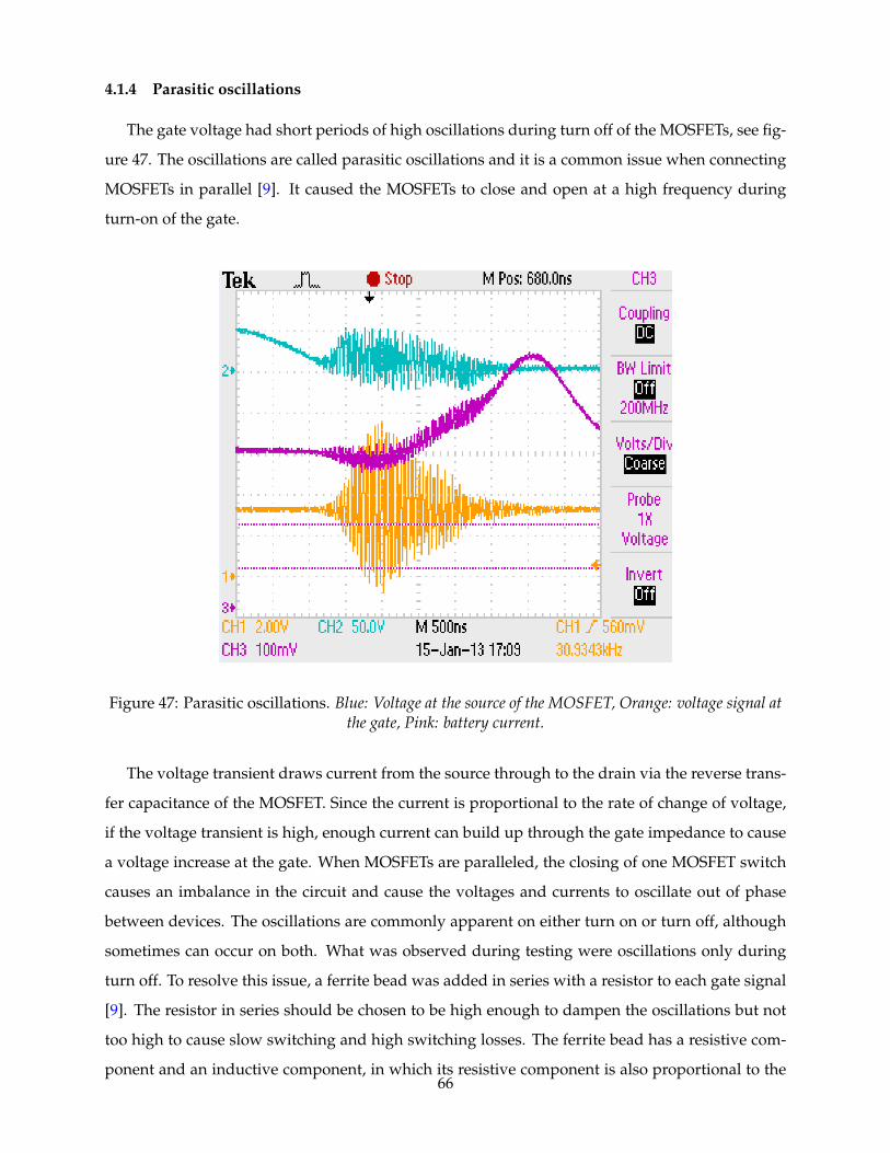
4.1.4 Parasitic oscillations
The gate voltage had short periods of high oscillations during turn off of the MOSFETs, see fig-
ure 47. The oscillations are called parasitic oscillations and it is a common issue when connecting
MOSFETs in parallel [9]. It caused the MOSFETs to close and open at a high frequency during
turn-on of the gate.
Figure 47: Parasitic oscillations. Blue: Voltage at the source of the MOSFET, Orange: voltage signal atthe gate, Pink: battery current.
The voltage transient draws current from the source through to the drain via the reverse trans-
fer capacitance of the MOSFET. Since the current is proportional to the rate of change of voltage,
if the voltage transient is high, enough current can build up through the gate impedance to cause
a voltage increase at the gate. When MOSFETs are paralleled, the closing of one MOSFET switch
causes an imbalance in the circuit and cause the voltages and currents to oscillate out of phase
between devices. The oscillations are commonly apparent on either turn on or turn off, although
sometimes can occur on both. What was observed during testing were oscillations only during
turn off. To resolve this issue, a ferrite bead was added in series with a resistor to each gate signal
[9]. The resistor in series should be chosen to be high enough to dampen the oscillations but not
too high to cause slow switching and high switching losses. The ferrite bead has a resistive com-
ponent and an inductive component, in which its resistive component is also proportional to the66
frequency of the system. Since the frequency is high the high impedance will dampen the oscil-
lations without much switching losses. Figure 48 shows the improvement after adding the ferrite
bead and series resistor.
Figure 48: Removal of parasitic oscillations with ferrite bead and series resistor to the gate Blue:Voltage at the source of the MOSFET, Orange: voltage signal at the gate, Pink: battery current.
4.1.5 Over-voltage on the gate
While doing the motor test, an over-voltage on the gate signal to the MOSFET occurred which
damaged the MOSFET and caused it to close permanently. This caused the motor to operate at
full power since the duty cycle became 100 percent. To ensure that this problem does not occur
again, zener diodes were added in shunt with each of the gate signals. The zener diode that was
chosen was the 1N5242B zener which has a nominal voltage of 12V. The zener diode will limit the
voltage on the gate to a safe turn on value of 12 V.
4.1.6 Reverse recovery current from diode
High reverse current during turn on of the diode was present during the load tests. The reverse
currents in the circuit were as high as 20A, when testing a 20A load. This issue needed to be
resolved since working with the larger loads can cause the higher reverse currents to damage the
circuit. Since the circuit deals with high voltages there will be a lot of charge in the depletion region
67
of the diode after being reverse biased. This will prevent the diode from entering its blocking
state. Instead there will be reverse current flowing through the diode for a short period of time
until internal recombination and the sweep out effect effect of the reverse current removes these
charge carries. Once the diode enters its blocking state after a large reverse current, it is possible
to see voltage transients across the diode. This occurs when inductance is present in the circuit
and surge suppression components are not present [cite]. If the circuit has switching elements the
effects of reverse currents through the diode is worse. This is because a reverse voltage can be
applied from switching to the diode before the inductive current has discharged so the diode may
continue in the forward biased mode resulting in a high surge current to the circuit [17].
Figure 49: Reverse current observed with the standard recovery diode Blue: Voltage at the source ofthe MOSFET, Yellow: Vds, Pink: diode current.
The solution to this problem is to use fast recovery rectifiers. The diode that was used previ-
ously was a standard recovery diode. The new diode that was purchased, Sanrex FRS300CA50
Fast Recovery Diode, is a high speed fast recovery diode designed for high power switching ap-
plications. The diode speed is at maximum 200ns. With the new diode the reverse current was
negligible; however, oscillations became more evident on the source voltage.
68
Figure 50: Reverse current removed with the standard recovery diode Blue: Voltage at the source ofthe MOSFET, Yellow: Voltage across Battery, Pink: diode current.
4.2 Controlling Switch-Node Ringing
4.2.1 Switch-node ringing
One of the problems encountered during our testing was oscillations at the source of the MOS-
FET as shown in Figure 52. The magnitude of the oscillations is proportional to the current through
the MOSFET. For the 20A load in Figure 52 the oscillation magnitude peak was at 92V. It is clear
that if we operate close to full load that the magnitude of these voltage oscillations could exceed
the absolute maximum rating for Vs which is 200V. Therefore possible solutions needed to be
investigated to reduce the oscillations.
69
Figure 51: Blue waveform: Voltage at source of the mosfet Yellow waveform: Vgs signal pink:N/A
4.2.2 The cause of switch-node ringing
Switch node ringing is caused by the parasitic capacitances and inductances from the diode,
MOSFET and gate drive circuit[2]. The parasitic inductances and capacitances for a buck converter
are shown in Figure 52. Due to the high switching frequency nature of the MOSFET, large voltage
and current transients are expected. These voltage transients appear as RC ringing at the source
of the MOSFET.
70
Figure 52: Parasitic Inductances and Capacitances of a Buck Converter [2]
4.2.3 How switch node-ringing occurs
At steady state when the MOSFET is off, the inductor and capacitor at the output supplies the
power to the load and also provide energy to the parasitic inductors and capacitances of the diode.
When the MOSFET turns on, the diode begins to turn off and the energy stored in the inductors
and capacitors are transfered to the MOSFETs parasitic elements. This transfer of energy causes
an RC ringing to appear at the source of the MOSFET [16]. The same process occurs when the
MOSFET turns off and diode turns on. The larger the current at the load the more energy that can
be stored in the parasitic elements. This increases the oscillation magnitude and can damage the
MOSFET.
4.2.4 Techniques to eliminate switch-node ringing
Increasing the gate resistance from the gate drive circuit helps reduce switch-node ringing by
increasing the turn on time. This allows the parasitic elements to discharge in a larger amount of
time. Unfortunately, this method is limited by the driving voltage of the gate driver. The larger
the gate resistance the larger the voltage drop across the resistor. If the gate resistance increases
too much there is not enough voltage to turn on the MOSFET. Furthermore, the switching losses
increase due to extension of turn on and turn off time. Therefore a better alternative is to use an71
RC snubber which will be discussed below.
4.2.5 Design of a RC snubber
The snubber circuit works by dampening the oscillations by providing a path for the energy
stored in the parasitic element to dissipate during switching of the MOSFET.
The process to design a snubber is as follows [[16]]:
1. Measure the ringing frequency, fc, of the voltage at Vs.
2. Put a snubber capacitor, C, across Vs to limit the ringing frequency to half the value.
3. The parasitic capacitance Cp of the diode (across Vs) is three times the value of C.
4. Calculate the parasitic inductance using equation fc = 12π√LC
.
5. Calculate the resistance to critically damp the oscillations using R =√L/C.
Figure 53 shows a close up of the switch-node oscillations at Vs without the snubber circuit.
From the oscilloscope capture we can see that fc =6.25MHz.
Figure 53: Switch-Node Oscillations at source of MOSFET
We used a 0.47uF in parallel with the diode and the oscillations decreased by a factor of twenty
as as shown in Figure 54. This indicates that the capacitance is much larger than it needs to be;72
however, due to having immediate access to the 0.47uF snubber capacitor, this capacitor was able
to be used to produce desired suppression of the oscillations on the source of the MOSFET.
Figure 54: Reducing the Source Ringing by a factor of twenty after adding C across diode
Since the oscillations were decreased by a factor of twenty and not two, it would be hard to
continue the process listed above. Instead, different resistance values were tested to get an ap-
propriate response. A resistance of 150 ohms was chosen, which resulted in a response as shown
below in Figure 55. Decreasing this resistance would result in a better response; however, also a
large power dissipation.
73
Figure 55: Source Ringing removed after an RC snubber placed across the diode
4.2.6 Non-DC output current to the motor
It is desired to have a steady current to the motor, however; the current output to the motor
ranges from zero to its peak value on every cycle. In the initial design, the LC filter at the Buck
output was not included. The inductance could not be increased into the mH range due to size
limitations on the amount of turns that can be wound by the large high-power wires around a
ferrite core. Therefore, to smooth the current, the LC circuit of the buck converter was placed back
into the circuit. The capacitor chosen was the AVX 100uF polypropylene film capacitor which was
able to provide a DC current output to the motor.
74
5 Final Design and Simulation Reconciliation
5.1 Final Design
Figure 56 displays the final design working without the intermediary wire connections so that
the main components can be seen easily. The metal box encloses the PCB and microcontroller
which will control all external components such as the contactor, throttle and power electronics.
The whole system has been modularized so that it can fit inside the electric motorcycle. The
controller is able to successfully control the current of the motor at no load as explained in the
following sections.
Figure 56: The final design of the power converter with the controller
5.2 Results and Simulation Reconciliation
The final design has been confirmed to work properly, but unfortunately various roadblocks
prevented a more detailed comparison of the simulation results to the hardware results. These
drawbacks are summarized below.
1. No access to Dynamometer: This prevented comparison of the motorcycle’s acceleration and
velocity to the simulation.75
2. Saturating current Probes: The current probes did not measure currents greater than 30A.
Even with these roadblocks, the controller was able to follow the current reference input from
the throttle accurately.
5.2.1 Hardware Results
Figure 57 shows the how the motorcycle was setup for the ”no load” tests. The back wheel was
raised off the ground.
Figure 57: Motorcycle with back wheel raised off the ground
Initial tests on the motorcycle were performed by using the throttle to control the current.
The throttle outputs 0-3.3V which corresponds to controlling 0-300A. For precautionary reasons
the current was limited. That means that if the maximum current reference was applied, the
microcontroller will limit the current reference to some programmed value. For example, the
maximum throttle was applied and the current reference was limited to 20A. Using our current
probe we we able to confirm that there was 20A at the motor current, Figure 58 shows the control
of a 20A current step.
76
Figure 58: Applying 20A current step to motor: blue: Voltage from MOSFET source to ground,green:Torque reference,yellow: Tamura Current sensor output to microcontroller, pink: Current probe
In Figure 58 the maximum torque reference is applied. The current probe outputs 1V for 10A.
One can see that the current is about 17A (this is due to ±3A accuracy of current sensor). The
current sensor measures 200mV which corresponds to 20A as seen from the current look up table
in Appendix C. Figure 59 illustrates the control of the current between ranges of 0 to 30A.
77
Figure 59: Varying zero to 30A current references to the motorblue: Voltage from MOSFET source toground,yellow: motor voltage, pink: Current probe
The current limit was increased to 60A and the current probe only measured 30A. Noticing that
output of the Tamura current sensor was reading 60A, so we knew something was wrong with the
probes. In order to confirm this a small series resistor of 0.5mΩ resistor was put in series with the
motor to measure the current. The resistor will output 50mV for 100A and 30mV for 60A. We redid
the tests for a 60A step and as Figure 60 shows we measured about 27.2mV which corresponds to
54.4A which confirms that the controller was working correctly. Please note that the signal is very
noisy because it is a resistor and only outputs in the mV range.
78
Figure 60: Applying 60A current step to motor and measuring voltage across 0.5mΩ Resistor
At this point we were confident that our controller was performing how we wanted to, but
we decided not to increase the current limit because the motor was unloaded and the wires we
were using would not be able to handle that current. We decided to wait until we got the brakes
working to load the motorcycle.
5.2.2 Simulation Reconciliation
Figure 61 shows 30A steps responses from our PSCAD simulation and our hardware response
with the same PI controller parameters.
79
Figure 61: Comparing a 30A current step from hardware [blue] and PSCAD results [red]
Comparison of the results are summarized in Table 3. There is clearly a big difference in percent
overshoot and rise time. Our PSCAD simulation is much faster while our hardware controller
seems to have a critically damped response.
Table 3: Comparison of Hardware and Simulation
Symbol PSCAD Response Hardware ResponsePercent Overshoot 44% 9%
Rise Time 2.1ms 56.9 msSteady State Error 0% 2.5%
Settling Time 29ms 71 ms
One reason why the results differ could be because because we cannot input a perfect step with
the throttle, which damps and slows down the response. Also the motor was not exactly at ”no
load” since it was turning the raised back wheel of the motorcycle. Even though our response of
56.9 ms is small in comparison to our simulation it is still reasonable fast to the human user, who
most likely would not notice the difference between a 1.9ms response and a 56 ms response.
In conclusion our controller did not meet the exact specifications of our simulation, but nonethe-
less it performed in a manner that would provide a fast response from the perspective of a human
applying the torque reference.
80
6 Conclusion
The purpose of this thesis project is to design and implement a controller to manage the acceler-
ation of a motorcycle through torque control of a PMDC brushed motor. The system was modeled
on an electromagnetic transient simulation software, PSCAD/EMTDC. The software simulation of
the hardware components include the battery, pre-charge circuit, dc-dc buck converter, motor and
mechanical system. Additionally, a PI controller was designed using the tool Simplex Optimiza-
tion from the PSCAD/EMTDC simulation software. The simulation performance characteristics
under no load set the criteria for the unloaded hardware system performance: Percent overshoot
≤ 44%; Settling time ≤ 29ms; and rise time ≤ 2.1ms.
Simplex Optimization determined the values required for the proportion and integral constants
to minimize the error between the actual torque and the reference torque. Alternatively, a more
analytical approach was obtained using system modeling of the load to perform a root locus anal-
ysis of the system with a PI controller. Through this method, the system can be designed to meet
more specific design requirements.
Once software simulations were complete, hardware testing was performed. A PCB was de-
signed to incorporate the low pass filters, regulators and gate drivers. Through hurdles that arose
in hardware testing, several design decisions were made: Ferrite beads were placed in series with
the gate signal to reduce parasitic oscillations of the gate voltage; zener diodes was added in
shunt with the gate signal to prevent overvoltage at the MOSFET gates; a fast recovery diode was
required to prevent reverse current and voltage transients across the diode; an RC snubber was
placed in shunt across the diode to reduce the oscillations observed at the source of the MOSFET;
and the LC filter of the buck converter was reinserted to smooth the output voltage.
Once all the hurdles were overcome, the motor torque was effectively controlled to follow the
torque reference set by the throttle using a PI controller. Hardware results show that the system
had a percent overshoot of 9% which meets the system maximum criteria of 44%. The hardware
results for steady state error and the settling time was 2.5% and 56.9ms respectively. Although
these did not meet the system criteria, the milisecond difference and small percent overshoot
between the hardware results and system critiria will not be differentiable by human perception;
therefore, the hardware results obtained are satisfactory.
The design of this electric motorcycle, along with other electric vehicles, expands the interest,
awareness and research conducted on the development of electric vehicles. This thesis has a sig-
nificant application to improve the condition of the environment which is being polluted by IECs.
The response of the general public to these environmental and economical concerns has lead to a
81
higher demand in electric vehicles. This design project opens the door for future undergraduate
projects to advance designs through additional features such as regenerative braking and alterna-
tive control techniques by providing a strong base to build upon. Through advances in electric
vehicle research, there is hope to see a positive impact on the environment for an eco-friendly and
sustainable future.
82
References
[1] B. Baker. (2004) Techniques that reduce system noise in adc circuits. [Online]. Available:
// Configurat ion B i t s#pragma conf ig FNOSC = PRIPLL // O s c i l l a t o r S e l e c t i o n//#pragma conf ig POSCMOD = EC#pragma conf ig FPLLIDIV = DIV 2 // PLL Input Divider#pragma conf ig FPLLMUL = MUL 20 // PLL M u l t i p l i e r#pragma conf ig FPLLODIV = DIV 1 // PLL Output Divider#pragma conf ig FPBDIV = DIV 1 // P er i p he r a l Clock d i v i s o r#pragma conf ig FSOSCEN = OFF // Secondary O s c i l l a t o r Enable
/∗Clock c o n t r o l S e t t i n g s∗/#pragma conf ig IESO = OFF // I n t e r n a l /Externa l Switch−over#pragma conf ig FCKSM = CSDCMD // Clock Switching & F a i l Safe Monitor#pragma conf ig OSCIOFNC = OFF // CLKO Enable
/∗USB S e t t i n g s∗///#pragma conf ig UPLLEN = ON // USB PLL enable//#pragma conf ig UPLLIDIV = DIV 2 // USB PLL input div ider//#pragma conf ig FVBUSONIO = OFF // VBUS pin c o n t r o l//#pragma conf ig FUSBIDIO = OFF // USBID pin c o n t r o l
#pragma conf ig FWDTEN = OFF // Watchdog Timer#pragma conf ig WDTPS = PS1 // Watchdog Timer P o s t s c a l e
#pragma conf ig POSCMOD = XT // Primary O s c i l l a t o r
#pragma conf ig CP = OFF // Code P r o t e c t#pragma conf ig BWP = OFF // Boot Flash Write P r o t e c t#pragma conf ig PWP = OFF // Program Flash Write P r o t e c t#pragma conf ig DEBUG = ON // Debugger Enabled#pragma conf ig ICESEL = ICS PGx1 // Page 3 of 3 4 : Cerebot MX7cK rm . pdf
#define SYS FREQ (80000000L )
//ADC// def ine setup parameters f o r OpenADC10#define PARAM1 ADC MODULE ON | ADC FORMAT INTG | ADC CLK AUTO| ADC_AUTO_SAMPLING_ON#define PARAM2 ADC VREF AVDD AVSS | ADC OFFSET CAL DISABLE| ADC_SCAN_OFF | ADC_SAMPLES_PER_INT_2 | ADC_ALT_BUF_ON| ADC_ALT_INPUT_ON#define PARAM3 ADC CONV CLK INTERNAL RC | ADC SAMPLE TIME 15#define PARAM4 ENABLE AN2 ANA | ENABLE AN3 ANA
88
#define PARAM5 SKIP SCAN ALL
//PI#define div ider 1343016 // Factor to normalize the output#define gain 6927366 // s c a l e to max f o r signed long i n t#define inv dt 50000 //inverse loop time (1/ period )#define intMAX 2147483640 //max f o r signed i n t#define MAX 1599 //(50kHz) 100% of max duty c y c l e#define MIN 0 //0% of max duty c y c l e#define inv Kp 200 //From Simulat ion#define Ki 200 //From Simulat ion
#include <p l i b . h>#define SYS FREQ (80000000)void systemInit (void )
// Outputs PWM s i g n a l onto OC1CON −−> Pin JD2 .// The duty c y c l e can be a l t e r e d by ://OC1RS ( note : max duty c y c l e = PR2 +1)// PWMperiod = [ ( PR2+1)∗1/(80 E6 )∗1 ]
#include <p l i b . h>
void PWMInit (void )INTEnableSystemMultiVectoredInt ( ) ;OC1CON = 0x0000 ; // Turn o f f the OC1OC1R = 0x0064 ; // I n i t i a l i z e primary Compare r e g i s t e rOC1RS = 0 ; // I n i t i a l i z e secondary Compare r e g i s t e rOC1CON = 0x0006 ; // Configure f o r PWM mode
//without Faul t pin enabled
PR2 = 1599 ; //50kHz
// Configure Timer2 i n t e r r u p t . Note t h a t in PWM mode , the// corresponding source t imer i n t e r r u p t f l a g i s a s s e r t e d .// OC i n t e r r u p t i s not generated in PWM mode .
IFS0CLR = 0x00000100 ; // Clear the T2 i n t e r r u p t f l a gIEC0SET = 0x00000100 ; // Enable T2 i n t e r r u p tIPC2SET = 0x0000001C ; // Set T2 i n t e r r u p t p r i o r i t y to 7T2CONSET = 0x8000 ; // Enable Timer2OC1CONSET = 0x8000 ; // Enable OC1
89
#include <p l i b . h>#include "Definitions.h"
void ADCInit (void )// conf igure and enable the ADCCloseADC10 ( ) ;
int PARAM1_2 = ADC_FORMAT_INTG | ADC_CLK_AUTO |ADC_AUTO_SAMPLING_ON ;
SetChanADC10 ( ADC_CH0_NEG_SAMPLEA_NVREF |ADC_CH0_POS_SAMPLEA_AN2 |ADC_CH0_NEG_SAMPLEB_NVREF | ADC_CH0_POS_SAMPLEB_AN3 ) ;// conf igure ADC using the parameters defined above
function [SOC ,D , Iold ] = DCA_ECE_15_1cycleV1 (N , y , SOC1 , D , Iold1 , E )%% COMPUTES 1 CYCLE of the ECE 15 Drive cycle%%%N = size of DriveCycle%y = velocity vector of Drive Cycle%SOC1 = State of Charge where initial value is hte SOC of the previous cycle%D = Distance%%% Initialization of variables
SOC = SOC1 ; %State of ChargeIold = Iold1 ; %Previous value of Current%Constantsurr = 0 . 0 0 2 ; %coef of rolling resistancep = 1 . 2 5 ; %Density of the airr = 0 . 2 9 5 9 ; %tyre radiusAf_Cd = . 6 ; %Frontal area∗Cd where Cd is the drag coefG = 4 ; %Gear ratiom = 2 0 0 ; %Massg = 9 . 8 ; %GravityI = 0 . 0 1 8 ; %moment of inertiang = 0 . 9 5 ; %gear system effienceyPac = 0 ; %accessory power (lights . . etc ) asumme negligable
% E = 4 8 ; %Battery voltagekc = 1 . 5 ; %Copper loss coefficientki = 0 . 1 ; %Iron loss coefficientkw = 0 . 0 0 0 0 1 ; %Windage loss coefficientConL = 2 0 ; % "constant losses" at any speed
%STARTfor C = 2 :N
%Calculate accelerationa = y (C ) − y (C−1) ; %acceleration/s