Design and Implementation of aMulti-Channel Field-Programmable
Analog Front-End For a NeuralRecording System
by
Bahareh Ebrahimi Sadrabadi
A thesispresented to the University of Waterloo
in fulfillment of thethesis requirement for the degree of
Master of Applied Sciencein
Electrical and Computer Engineering
Waterloo, Ontario, Canada, 2014
c© Bahareh Ebrahimi Sadrabadi 2014
Author’s Decleration
I hereby declare that I am the sole author of this thesis. This is a true copy of the thesis,including any required final revisions, as accepted by my examiners.
I understand that my thesis may be made electronically available to the public.
Bahareh Ebrahimi Sadrabadi
ii
Abstract
Neural recording systems have attracted an increasing amount of attention in recentyears, and researchers have put major efforts into designing and developing devices thatcan record and monitor neural activity. Understanding the functionality of neurons can beused to develop neuroprosthetics for restoring damages in the nervous system. An analogfront-end block is one of the main components in such systems, by which the neuron signalsare amplified and processed for further analysis.
In this work, our goal is to design and implement a field-programmable 16-channelanalog front-end block, where its programmability is used to deal with process variation inthe chip. Each channel consists of a two-stage amplifier as well as a band-pass filter withdigitally tunable low corner frequency. The 16 recording channels are designed using fourdifferent architectures. The first group of recording channels employs one low-noise ampli-fier (LNA) as the first-stage amplifier and a fully differential amplifier for the second stagealong with an NMOS transistor in the feedback loop. In the second group of architectures,we use an LNA as the first stage and a single-ended amplifier for implementing the secondstage. Groups three and four have the same design as groups one and two; however theNMOS transistor in the feedback loop is replaced by two PMOS transistors.
In our design, the circuits are optimized for low noise and low power consumption. Sim-ulations result in input-referred noise of 6.9 µVrms over 0.1 Hz to 1 GHz. Our experimentsshow the recording channel has a gain of 77.5 dB. The chip is fabricated in AMS 0.35 µmCMOS technology for a total die area of 3 mm×3 mm and consumes 2.7 mW power froma 3.3 V supply. Moreover, the chip is tested on a PCB board that can be employed forin-vivo recording.
iii
Acknowledgements
First and foremost, I thank God Almighty for giving me grace, health and privilege to
pursue my education and his blessing in giving me life, health and intelligence.
I would like to thank my supervisor Dr. Vincent Gaudet and express my sincere ap-
preciation and gratitude to him for his guidance, support and confidence in me and my
work.
Many thanks to Dr. Ajoy Opal and Dr. Peter Levine for reading and reviewing my
thesis, and giving me invaluable comments
In particular, thank you to Brendan Crowley for all his support, teaching and guidance.
I am also thankful to all amazing members in our group, for making my life during the past
two years a fun, challenging and memorable one. Especially, I would like to thank Navid
Bahrani, Manpreet Singh and Chris Ceroici to name a few, for their insightful comments
and helpful discussions.
The University of Waterloo offers a rich and productive environment to explore new
ideas. I am grateful to have the chance to study in the middle of a greatly supportive
community and be surrounded by wonderful colleagues.
My family has been an integral part of my academic life. Despite being many thousands
of kilometers away, their support and constant courage gave me the strength to persevere
me through these many years as a student. There are no words that can express my
gratitude and appreciation for all you have done and been for me.
iv
Dedication
I would like to dedicate this thesis to my parents, and my husband for their endless love,limitless encouragement, and sacrifice throughout my Masters.
v
Table of Contents
List of Tables viii
List of Figures ix
Nomenclature xi
1 Introduction 1
1.1 Motivation . . . . . . . . . . . . . . . . . . . . . . . . . . . . . . . . . . . . 1
1.2 Thesis Organization . . . . . . . . . . . . . . . . . . . . . . . . . . . . . . . 4
2 Background 5
2.1 Characteristics of Neural Signals . . . . . . . . . . . . . . . . . . . . . . . . 5
2.1.1 Resting Potential . . . . . . . . . . . . . . . . . . . . . . . . . . . . 5
2.1.2 Action Potentials . . . . . . . . . . . . . . . . . . . . . . . . . . . . 7
2.2 Neural Recording Techniques . . . . . . . . . . . . . . . . . . . . . . . . . 9
2.3 Characteristics of Neural Recording Systems . . . . . . . . . . . . . . . . . 11
2.4 State-of-the-Art Neural Recording . . . . . . . . . . . . . . . . . . . . . . . 12
3 Design and Simulation of Neural Recording Analog Front-End 18
3.1 Recording Channel Architecture . . . . . . . . . . . . . . . . . . . . . . . . 18
3.2 Design of LNA . . . . . . . . . . . . . . . . . . . . . . . . . . . . . . . . . 24
3.3 Design of Second-Stage Amplifier . . . . . . . . . . . . . . . . . . . . . . . 28
vi
3.4 Design of DACs . . . . . . . . . . . . . . . . . . . . . . . . . . . . . . . . . 33
3.5 Testability . . . . . . . . . . . . . . . . . . . . . . . . . . . . . . . . . . . 34
3.6 Design of MUXs . . . . . . . . . . . . . . . . . . . . . . . . . . . . . . . . . 38
4 Simulation and Measurement Results 43
4.1 Simulation Results . . . . . . . . . . . . . . . . . . . . . . . . . . . . . . . 43
4.2 Design of AF5 PCB . . . . . . . . . . . . . . . . . . . . . . . . . . . . . . . 49
4.3 Test Results . . . . . . . . . . . . . . . . . . . . . . . . . . . . . . . . . . . 51
5 Conclusions 56
5.1 Summary of the Work and Contributions . . . . . . . . . . . . . . . . . . . 56
5.2 Future Work . . . . . . . . . . . . . . . . . . . . . . . . . . . . . . . . . . . 57
APPENDICES 59
A Current and Voltage Reference 60
A.1 Design of Current Reference . . . . . . . . . . . . . . . . . . . . . . . . . . 60
A.2 Simulation and Test Results . . . . . . . . . . . . . . . . . . . . . . . . . . 65
B Simulation Results of Other Blocks 66
References 70
vii
List of Tables
2.1 Distribution of ions around a neuronal membrane. . . . . . . . . . . . . . . 6
2.2 Comparison of state-of-the-art analog front-ends for neural recording sys-tems . . . . . . . . . . . . . . . . . . . . . . . . . . . . . . . . . . . . . . . 17
3.1 Comparison of different op-amp topologies. Adapted from [48] . . . . . . . 24
3.2 Transistor sizing of LNA and its CMFB circuit. . . . . . . . . . . . . . . . 25
3.3 Transistor sizing of folded-cascode amplifier circuit. . . . . . . . . . . . . . 30
3.4 Transistor sizing of CMFB Circuit for fully-differential folded-cascode am-plifier. . . . . . . . . . . . . . . . . . . . . . . . . . . . . . . . . . . . . . . 31
3.5 Capacitor values for channel architecture (F) . . . . . . . . . . . . . . . . . 32
3.6 Transistor sizing of Miller amplifier. . . . . . . . . . . . . . . . . . . . . . . 36
4.1 Simulation results for different blocks. . . . . . . . . . . . . . . . . . . . . . 48
4.2 Functionality of different recording channels . . . . . . . . . . . . . . . . . 54
4.3 Test and Simulation results for different blocks . . . . . . . . . . . . . . . . 55
4.4 Measurement results of the AF5 chip . . . . . . . . . . . . . . . . . . . . . 55
A.1 Transistor sizing of BMR circuit. . . . . . . . . . . . . . . . . . . . . . . . 62
A.2 Transistor sizing of LNA-biasing . . . . . . . . . . . . . . . . . . . . . . . . 64
A.3 Transistor sizing of folded-cascode biasing . . . . . . . . . . . . . . . . . . 64
A.4 Simulation and test results of biasing voltages . . . . . . . . . . . . . . . . 65
viii
List of Figures
2.1 Functionality of an action potential . . . . . . . . . . . . . . . . . . . . . . 8
3.1 Band-pass filter for rejection of electrode DC offset . . . . . . . . . . . . . 19
3.2 Architecture of block 1 of recording channel’s front-end. . . . . . . . . . . . 21
3.3 Architecture of block 2 of recording channel’s front-end. . . . . . . . . . . . 22
3.4 Architecture of block 3 of recording channel’s front-end. . . . . . . . . . . . 23
3.5 Architecture of block 4 of recording channel’s front-end. . . . . . . . . . . . 23
3.6 Schematic of LNA circuit and its CMFB circuit. . . . . . . . . . . . . . . . 25
3.7 Schematic of single-ended folded-cascode amplifier circuit. . . . . . . . . . 28
3.8 Schematic of fully differential folded-cascode amplifier circuit. . . . . . . . 30
3.9 Schematic of CMFB circuit for fully differential folded-cascode amplifier. . 31
3.10 Frequency response of LNA with a varying bias voltage from 1.2 V to 2 Vwith 25mV steps. . . . . . . . . . . . . . . . . . . . . . . . . . . . . . . . . 33
3.11 Architecture of 5-bit DAC circuit. . . . . . . . . . . . . . . . . . . . . . . . 35
3.12 Architecture of one block . . . . . . . . . . . . . . . . . . . . . . . . . . . . 37
3.13 Schematic of Miller Amplifier circuit . . . . . . . . . . . . . . . . . . . . . 38
3.14 Schematic of Fully differential MUX cell . . . . . . . . . . . . . . . . . . . 39
3.15 Schematic of 8X1 MUX circuit . . . . . . . . . . . . . . . . . . . . . . . . . 40
3.16 Architecture of 32X1 MUX (5-bit) circuit for DAC . . . . . . . . . . . . . 41
3.17 Schematic of 8X1 MUX circuit for DAC . . . . . . . . . . . . . . . . . . . 42
3.18 Architecture of digital block . . . . . . . . . . . . . . . . . . . . . . . . . . 42
ix
4.1 (a) Frequency response (b) Transient simulation of the LNA with PMOStransistor in feedback (blocks 3 & 4) with an input signal of 3 mV at 1 kHz 44
4.2 Noise simulation of LNA with PMOS transistor in feedback (blocks 3 & 4). 45
4.3 Frequency response of the second-stage amplifier with PMOS transistor infeedback (blocks 3). . . . . . . . . . . . . . . . . . . . . . . . . . . . . . . 46
4.4 Frequency response of the recording channel with PMOS transistor in feed-back (block 3). . . . . . . . . . . . . . . . . . . . . . . . . . . . . . . . . . . 46
4.5 AC simulation of the recording channel (blocks 3) for process variation. . 47
4.6 Simulated total harmonic distortion of recording channel (block 3) with ainput voltage varies from 200 µV to 600 µV . . . . . . . . . . . . . . . . . 48
4.7 Die Photo of 16-channel neural recording . . . . . . . . . . . . . . . . . . . 49
4.8 AF5PCB board . . . . . . . . . . . . . . . . . . . . . . . . . . . . . . . . . 50
4.9 Output signal of the LNA with PMOS in feedback (channel 10). . . . . . . 52
4.10 Output signals of a fully differential recording channel with PMOS in feed-back (channel 10). . . . . . . . . . . . . . . . . . . . . . . . . . . . . . . . 52
4.11 Measured frequency response of the LNA with PMOS in feedback (channel10) with different DAC values. . . . . . . . . . . . . . . . . . . . . . . . . . 53
4.12 Measured noise of recording channel for block 10 . . . . . . . . . . . . . . . 54
A.1 Schematic of Beta multiplier reference circuit . . . . . . . . . . . . . . . . 61
A.2 Schematic of biasing circuit for telescopic and folded-cascode amplifier . . . 64
B.1 Frequency response of the recording channels for block 1 . . . . . . . . . . 67
B.2 Frequency response of the recording channels for block 2 . . . . . . . . . . 67
B.3 Frequency response of the recording channels for block 4 . . . . . . . . . . 68
B.4 Simulated total harmonic distortion for each block . . . . . . . . . . . . . . 69
x
Nomenclature
ADC Analog to Digital Converter
BMR Beta Multiplier Reference
CM Common Mode
CMFB Common Mode Feedback
CMRR Common Mode Rejection Ratio
DAC Digital to Analog Converter
LNA Low Noise Amplifier
PSRR Power Supply Rejection Ratio
SNR Signal to Noise Ratio
THD Total Harmonic Distortion
xi
Chapter 1
Introduction
1.1 Motivation
Recent decades have seen growing interest in understanding how the human brain and the
nervous system operate. With the rapid advance in neural science, much information has
been learnt about human neural networks and the neuron as its basic component. Neurons
are excitable cells that collect, process and transmit information through neural systems
by the aid of chemical signals [58]. Therefore, further observation of reactions happening
in neurons can improve our knowledge about the functionality of the nervous system. A
better understanding of neurons may enable us to address a wide range of neurological
symptoms and disorders, such as Epilepsy and Parkinson’s disease [33].
Epilepsy covers a group of long-term neurological disorders that affect around one
percent of people [40]. The disease is characterized by epileptic seizures that are typically
1
caused by abrupt and excessive electrical discharge in a group of neurons. Such seizures
are recurrent and may vary from brief lapses of attention to severe and prolonged seizure
activities [46]. The unexpected nature of most seizures introduce significant trouble into
patients’ lives and impact their families. Unfortunately, there is no permanent cure for
epilepsy, but it can be controlled by medications or surgery. Around thirty percent of
patients do not have access to these methods [15]. However, electrically stimulating certain
parts of the brain may considerably reduce the frequency and intensity of seizures [20].
Parkinson’s is another common nervous system deficiency, and is known to be a degen-
erative neurological disorder of the central nervous system. Parkinson’s affects the motor
control of the brain [46]. Its symptoms usually include tremors at rest, difficulty in ini-
tiating movement, uncontrolled movements, and muscle stiffness to name a few. To date
[46], the main cause of Parkinson’s disease is not known, although some atypical cases
have a genetic origin [46]. As such, no definitive cure has been found, but it is shown that
stimulating the brain decreases the tremors [32].
Electrically stimulating the brain to mitigate neurological symptoms requires accurate
understanding of neurons and their performance. For this purpose, we should record and
analyze neural activities in their normal and excited modes. The detail of this analysis
helps us to determine a proper pattern for stimulating the brain [9][20]. Moreover, we may
be able to restore neurons’ functions in parts of the nervous system damaged by different
diseases or paralysis.
Scientists carried out initial attempts to explore neurons’ activities by observing ani-
mals’ neural networks, and they gained invaluable information about the nervous system
2
and its operations [13][54]. For example, they detected and recorded the action potentials
of many neurons corresponding to motor planning or control to develop analytic models
that predict hand trajectories in real time [60]. They were eventually able to use the model
in prosthetic devices and simulate hand movements in humans [28]. Furthermore, recent
clinical experiments with paralyzed human volunteers have demonstrated that it is feasible
to develop prosthetic devices that are controlled directly by thoughts, if the activity of
multiple neurons can be observed [28]. Therefore, researchers try to record and process
the neural activities in human brains to facilitate controlling different devices with human
thoughts. This technology has a significant impact on people with disabilities as it offers
the hope of restoring their abilities in the near future.
Neural recording systems have attracted an increasing amount of attention in recent
years, and researchers have put major efforts into designing and developing devices that
can record and monitor neural activities. One of the core components in such systems is
known as the analog front-end block. The neural signals are entered into this block after
recording by electrodes. The analog front-end block then amplifies the signals to make
them suitable for further processing.
In this thesis, we aim to design and implement a mixed-signal field-programmable
analog front-end block using AMS 0.35 µm CMOS technology. The chip is comprised of
16 recording channels with the ability to tune the low corner frequency response digitally
to cope with process variation. To examine various architectures, the recording channels
are designed using four different configurations. Our experiments show promising results
and prove the design’s potential as one of the initial works in the area of neural recording
systems. Based on our results, we intend to use the design in an up coming set of in vivo
3
experiments, led by our clinical partners.
1.2 Thesis Organization
This chapter presents the motivation for this work. The organization of the thesis chapters
is as follows.
• Chapter 2 presents the background related to neuron functionality. The different
recording techniques and the characteristics of a neural recording system are then
explained. A review on the works of different research groups involved in the design
of neural recording systems are described next.
• The design details of an analog front-end for neural recording systems is described
in Chapter 3. Preferred architectures for each block will be discussed based on the
system specification, and then the circuit of interest, with its design details, will be
provided.
• Chapter 4 includes our experiments and demonstrates the simulation results. Then,
the design of a PCB, used for testing our chip design, will be discussed. The chapter
ends with our the test results.
• Chapter 5 summarizes the work to date and the suggested work that can be done in
the future.
4
Chapter 2
Background
2.1 Characteristics of Neural Signals
Neuron cells are the most fundamental elements in the nervous system as they transfer in-
formation throughout the body [58]. Anyone working on neural recording systems requires
an understanding of neurons. This section presents relevant background about neurons
and their activities.
2.1.1 Resting Potential
Neurons, like all other cells in the body, have a cell membrane with various ions distributed
around it. Table 2.1 shows the distribution of the ions across the membrane in a neuron
cell in a resting state [8]. These ions are distributed unequally around the membrane.
Concentrations of K+ ions are mostly inside the cell (intracellular), and NA+ ions are
5
mostly concentrated outside the cell (extracellular). There also exist other ions such as
Ca2+ and Cl−, in lower concentrations [8].
An ion-pump comprised of protein in the cell membrane pumps different ions into or
out of the neuron. It also helps to keep the concentration of intracellular and extracellular
ions in their resting state values [58] . The Na+-K+ pump, which uses ATP to operate, is
one of the most important mechanisms that preserves the high concentration of K+ and
Na+ inside and outside of the cell, respectively. The pump acts by pumping two K+ ions
into the cell and three Na+ outside the neuron. These two ions are uninterruptedly diffused
across the membrane [58].
Table 2.1: Distribution of ions around a neuronal membrane.
Ions extracellular value (mM) intracellular value (mM)Na+ 155 20K+ 3 140Cl− 130 8A− 25 162Ca2+ 1.2 10−4
It can be observed that the electric charge across a membrane in the resting state is
not zero, and thus a so-called resting potential exists inside the neuron with respect to the
outside of the neuron. The net flow of each ion across the membrane is zero at a particular
voltage. At this voltage, the concentration gradient and electrical gradient of the ion reach
equilibrium, so we call this voltage equilibrium potential [8]. The voltage is calculated
using Nernst’s equation (2.1). For instance, the equilibrium potentials calculated for Na+
6
and K+ at 37 C are equal to +55 mV and -103 mV, respectively [8].
EX =RT
ZxFln
[X]o[X]i
, (2.1)
where R is the universal gas constant, T is the temperature in K, F is the Faraday Constant,
and ZX is the valency of ion x. [X]o and [X]i are the external and internal concentrations
of the ion x, respectively.
The resting potential depends on the permeability and equilibrium potential of all
different ions across the membrane. If the permeability of K+ and Na+ are equal, the
resting potential will be in between their equilibrium potential and equal to -48 mV. In the
resting state, the K+ ion permeability is dominant; thus, the resting potential would be
close to the equilibrium potential of K+ ions than that of Na+. Calculations show that the
resting potential is typically around -60 to -70 mV [8][58].
2.1.2 Action Potentials
Neurons are known as excited cells and can generate spikes at the time of stimulation [58].
These spikes are called action potentials and can be produced with the aid of ion channels,
which are macromolecular pores made from protein in the cell membrane. They control
the flow of ions by opening and closing the gate to shape electrical signals in neurons, and
create an action potential, which is the response in the nervous system. Each channel is
ion-specific and lets only one ion flow through it [27].
The ion channels existing in neurons are voltage-gated ion channels, meaning that these
7
Figure 2.1: Functionality of an action potential
ion channels will open if stimulation is large enough to exceed their threshold potential.
Figure 2.1 illustrates the different phases of an action potential occurrence. When a neuron
is sufficiently stimulated, the Na+ ion channels open and diffuse Na+ ions through the cell,
causing increased potential (phase1). The potential required for opening K+ ions is larger
than that needed for Na+ ions. Therefore, when the membranes’ potential is high enough,
the K+ channels open. The Na+ channels close after 1ms. These two incidents produce
phase 2, which decreases the membrane potential toward the resting potential level. The
K+ ion channel will be closed for a period after that of Na+, resulting in an undershoot
in phase 3. Eventually, the membrane potential will reach the resting state with the help
of ion pumps [58]. Experiments show that the action potentials in humans are typically
pulses with a duration of approximately 1 msec and amplitude of 100 mV [8].
8
2.2 Neural Recording Techniques
The neural signals that are recorded by arrays of micro-electrodes can be categorized into
two major groups: action potential and field potential [43]. The neural signals in these
two groups differ mainly in their characteristics, such as signal bandwidth, amplitude and
function.
The action potential signals can be obtained by either intracellular or extracellular
method. In order to do intracellular recording, a sharp micro-electrode is typically inserted
inside the cell. Using this method, we are able to measure up to 100 mV. However, the
micro-electrode penetrates the cell causing cell death within a few minutes, and thus such
electrodes are not appropriate for chronic implants [26]. To avoid penetrating cells, a
micro-electrode with a sufficiently small tip is used for extracellular recordings [43]. In
this method, the micro-electrode is placed adjacent to the neuron, and so the neuron
action potential or spike is much smaller than that obtained with intracellular recording.
Usually, the amplitude of the neural signals using extracellular recording is around 50 ∼
500 µV, with a bandwidth of 100 Hz to 6 kHz [39]. Extracellular recording is sometimes
a challenging task. For example, recording the activities of multiple neurons located in a
single region of the brain often requires an array of recording electrodes. Moreover, two
or more independent neurons may contribute to the output of a single recording electrode,
and thus they should be differentiated according to the action potential waveform using
signal processing software [43]. This is often called multi-unit recording.
One common neural recording approach is known as a field potential. In the nervous
system, individual neurons produce an electric field. The integration of these fields results
9
in a local field potential [43]. The activities of the neurons can be recorded by interact-
ing with these fields and with the aid of three major methods: local field potential (LFP),
electrocorticograms (ECoG) and non-invasive scalp-recorded electroencephalograms (EEG)
[4]. In LFP, the electrophysiological signal generated by a local field is recorded with a
low impedance extracellular micro-electrode. The micro-electrode is located far from local
neurons to alleviate the domination of any particular cell in measuring the electrophysio-
logical signal [34]. The recording in ECoGs is done by an electrode implanted inside the
skull yet outside the brain, providing an invasive method while preserving signal quality
[55]. A method is called invasive when the neuron activity is recorded directly from the
cortex under the skull. Such methods require surgery and provide high spatial and time
resolution at the same time. An EEG is a non-invasive approach in which the electrical field
changes are recorded by placing electrodes on the scalp [4]. The LFP method is preferred
to record the activity of a group of neurons located within millimeters of the recording
electrode in the tissue of interest. In contrast, ECoGs and EEGs collect the neural signals
over much larger areas, such as several square centimeters at the cortical surface and scalp,
respectively [4]. In addition, unlike the other two methods, which focus on specific neural
signals, EEGs can provide a big picture of the brain that is quite helpful in many applica-
tions [43]. In general, electrodes on the brain, cortex or scalp surface provide signals that
have a far lower amplitude than action potential recordings, and thus they have much less
specific-time resolution.
10
2.3 Characteristics of Neural Recording Systems
A neural recording system should have various characteristics. To reduce the possibility
of infection during clinical experience, having a fully implantable system is one of the
key factors in the design of neural recording devices [22]. Therefore, wireless features
are appealing for neural recording systems. The use of wireless communication for such
systems enables patients to have free movement and avoids the typical difficulties arising
with wired systems [31]. Moreover, wireless systems let researchers carry out their tests
on various animals.
A wire line supply voltage cannot be used in fully implantable circuits due to the high
risk of infection [31]. One of the best options is to use a battery as the power supply.
The battery should be rechargeable, since repeated surgeries are not desirable. Finding
appropriate small-size and long-lifetime batteries is a challenge. A wireless power circuit
is also an option [22] for overcoming power-supply issues.
The power dissipation of implants causes heat, which kills the tissues surrounding
electrodes. Research shows that an increase of even 1C in temperature equals 80 mW/cm2
power density dissipation, which puts healthy cells in severe danger [50]. The higher power
dissipation also causes a shorter battery lifetime and requires a larger size battery; thus,
the power consumption of the device should be small enough to prevent damage to human
tissues. Last but not least, the battery should preferably work for eight to ten years.
The extracellular potential recorded from neural signals is very small, typically in the
range of 50 µV to 500 µV [26], and so it is necessary to have very small input-referred
noise in the interface of such recording systems.
11
A neural recording chip should also have small enough dimensions in the order of
millimetres, as it is feasible to implant small chips in the body [14]. Small size chip also
considerably decreases damage to human tissues. The maximum size of a chip varies based
on the position of the implant in the body. Smaller chips also reduce the fabrication cost.
Typically, a human body treats any implanted device as a foreign substance. Thus,
bio-compatibility plays a core role in device implementation and is very important for
realizing a clinically implantable device. It is essential to design and develop implants in
a way that introduces minimal intrusion to the body. Protecting the implant itself is a
separate major challenge, that is beyond the scope of this thesis.
2.4 State-of-the-Art Neural Recording
In 1952, Hodgkin and Huxley [29] pioneered a model for generating action potential and
understanding how neurons work using intracellular recording. Great interest has been
shown in the neural recording field from that time, and several research groups have been
working on this area. Major progress has been achieved in the analog front-end circuits of
neural recording systems. Recent state-of-the-art methods will be discussed in this section.
The initial neural recording circuits were developed using discrete components in the
1970s [59][17][62] due to difficulties in integrating circuits and problems in fabrication.
These circuits were not implantable because of their large sizes and high power consump-
tion. Some sensors like blood-pressure and flow meters were also introduced between 1960
and the 1970s [45][49][47][19][16].
12
For the first time, in 1986, K. Najafi and K. D. Wise proposed an IC-compatible
multichannel recording array using an on-chip circuitry [39]. The circuit included amplifiers
with a gain of 100, an analog multiplexer and a unity gain output buffer. Moreover, it
performed with a 5V supply voltage. The chip was 1.3 mm2 in size and dissipated 5 mW
of power. The group tried to extend their work, and in 1992, J. Ji and K. D. Wise [30]
introduced an analog front-end with a second-generation of their probes. The proposed
circuit includes an amplifier with higher gain (300) than the previous one, as well as a
band-pass filter for limiting the low and high frequency to 15 Hz and 7 kHz, respectively.
The die area of the circuit is 2.5 mm2 and its equivalent input noise integrating from 100 Hz
to 10 kHz is 15µVrms. It works with a 5V voltage and dissipates 2.5 mW. T. Alun and K.
Najafi [1] developed a telemetrically powered neural recording system with multichannel,
fully integrated circuitry in a bipolar CMOS process in 1998. The front-end includes l00 Hz
to 3.1 kHz band limited amplifiers, a multiplexer, and an ADC and RF interface circuitry.
The front-end operates with a 5V supply and dissipates 10 mW of power. Its size is 4x4
mm2. In 2003, R. H. Olsson et al. [42] designed a fully integrated band-pass amplifier for
neural recording systems. It uses diode-connected NMOS transistors that are biased in
the sub-threshold region in the feedback loop of the amplifier as we will use in our work.
The AC gain of the amplifier equals 38.2 dB, and it has low and high cut-off frequencies of
66 mHz and 24 kHz, respectively. The circuit works with a 1.5V supply, and it dissipates
92µW. The input-referred noise of the circuit integrated from 100 Hz-10 kHz is 16.6 µVrms
and has a 0.82 mm2 area. The aforementioned group have also worked on wireless blocks of
the system and has introduced different circuits [52][10]. Finally, in 2009, A. M. Sodagar et
al. developed the most recent implantable neural recording system to date from this group
13
[53]. The 64-channel neural recording system sends spike data to an external interface
wirelessly. The system operates with a 1.8 V supply and consumes 14.4 mW. It takes 2170
mm2 of die area, and its input-referred noise is 8 µVrms. The analog front-end part was
implemented in a commercial 0.5 µM CMOS process and includes 64 amplifier channels.
The amplifier gain and high-frequency cut-off equal 59.5 dB and 9.1 kHz, respectively. The
low frequency corner of the amplifier can be adjusted from sub-Hertz to a few hundred
Hertz. The amplifier dissipates 75 µW, and the size of each channel is 0.072 mm2. In 2010,
G. E. Perlin and K. D. Wise [44] proposed a new probe and 64-channel analog front-end
with the ability of programmable gain from 40 dB to 60 dB digitally . The equivalent input
noise of opamp from 10 Hz to 10 kHz is 4.8 µVrms. The low-frequency cutoff is adjustable
from 10 Hz to 100 Hz and the high cutoff frequency is 9.1 kHz. The circuit is fabricated
in 0.5 µm with 14.88 mm2 die area. It also dissipates 50 µW power.
In [24], R. R. Harrison and his colleagues at the University of Utah developed a low-noise
and low-power bio-amplifier for neural recording systems. The topology has a MOS-bipolar
pseudo-resistor in the feedback loop. The gain of the amplifier is equal to 39.5 dB, and
it rejects all DC offset. The low and high corner frequencies of the amplifier are 0.025
Hz and 7.2 kHz, respectively, and the input-referred noise over the band is 2.2 µVrms.
The chip has 0.16 mm2 of die area and is built in a standard 1.5 µm CMOS process.
It dissipates 80 µW at 2.5 V supply voltage. In 2006, P. T. Watkins et al. introduced
a wireless multichannel, fully implantable neural recording system [56].The chip contains
amplifiers, ADC and circuitry for spike detection as well as FSK data transmission. The
88-channel chip contains a 60 dB amplifier in the frequency range of 1 kHz to 5 kHz and
input-referred noise of 5.1 µVrms. The total chip dissipates 13.5 mW of power and has a 27.3
14
mm2 area. In 2007, R. R. Harrison designed a 16-channel front-end for neural recording
systems with a tunable high frequency [23]. This chip has the ability to record different
types of bioelectrical signals such as EEG, EMG, ECG, etc. Each channel consists of two
amplifiers, with the gain of each amplifier equal to 46 dB, and its low-frequency cutoff is
0.05 Hz. The high frequency of the amplifier can be adjusted in the range of 10 Hz to
10 kHz according to the type of signal by using two off-chip resistors. The input-referred
noise for each amplifier is 2 µVrms. The chip is built using a 0.6 µm CMOS process, and
the total dissipated power with fH = 10 kHz is 41 mW. Finally, in 2009, R. R. Harrison
et al. proposed a 100-channel integrated circuit for wireless neural recording systems [25].
The chip contains amplifiers, 10-bit ADC and a transmitter for sending out the data. The
amplifier has a 60 dB gain with programmable low and high cut-off frequency.
Another group working in the design of neural recording systems is at the University
of Toronto under the supervision of R. Genov. In 2007, J. Aziz et al. [5] designed a
256-channel analog front end for neural recording systems. The chip was fabricated in
0.35 µm and has a 13.5 mm2 size. Each channel has a two-stage amplifier with band pass
filter with a sub-hertz low cutoff frequency and tunable high cutoff frequency from 1 kHz
to 10 kHz. The amplifiers used in the chip are single-ended, with sample and hold cells.
The gain of the channel is also programmable with values of 200,1000,2500,5000. The
chip operates at 3.3V, with a power dissipation of 6 mW and input-referred noise of 13 µV
integrating from 10 Hz to 10 kHz. R. Shulyzki et al. reported a closed-loop neural recording
and stimulation system in 2011 [51]. The chip records the extracellular neurons’ potential
using 256 channels. Then, based on the given data taken from the recording channels, it
generates stimulation signals for 64 channels. The analog front-end of the recording part
15
is comprised of two-stages fully differential with a adjustable low cutoff frequency. It also
has a sample-and-hold cell and an ADC. The gain of the channel is programmable in 8
modes from 54 dB to 72 dB. The chip is in 0.35 µm technology and dissipates an overall
power of 13.5 mW. The input-referred noise of one recording channel is 7.99 µVrms.
In 2006, Liu et al. from the the University of California at Santa Cruz designed a
wireless system for recording the neural activity of sharks. The chip consists of amplifiers,
a multiplexer and an off-chip ADC and telemetry circuit [36]. It is fabricated in a 0.18
µm process and consumes 18µW, and the input-referred noise is equal to 8.5µVrms. To
have a high CMRR, a wide swing current mirror is used in OTA. The designed amplifier
has 100 dB voltage gain, with the corner frequency of 1 Hz to 10 kHz. In 2011, the same
group developed a 64-channel fully integrated analog front-end [37]. Every channel has a
two-stage amplifier with adjustable gain and corner frequency. Each of the 32 recording
channels then has a 32X1 MUX and an ADC. The chip is fabricated in 65 nm technology
and operates at 1.2V. The overall power consumption of the chip is equal to 2.56 mW, and
the input-referred noise is 3.8µVrms integrating from 30 Hz to 100 kHz. The gain of the
amplifier is tunable in the range of 47 to 59 dB. Table 2.2 shows a comparison between
some of the state-of-the-art works mentioned here.
16
Tab
le2.
2:C
ompar
ison
ofst
ate-
of-t
he-
art
anal
ogfr
ont-
ends
for
neu
ral
reco
rdin
gsy
stem
sR
ef.
Unit
s[4
2][2
4][2
3][5
3][4
4][5
1][3
7]T
his
wor
kN
um
ber
ofC
han
nel
s-
11
1664
6425
664
16G
ain
dB
38.2
39.5
4659
.540
-60
53-7
247
-59
77.5
Input-
refe
rred
noi
seµ
Vrm
s16
.62.
22
84.
87.
993.
86.
9P
ower
Supply
V±
1.5±
2.5
51.
8±
1.5
31.
23.
3P
ower
Dis
sipat
ion
for
one
chan
nel
µW
9280
460
7550
52-
125
Low
Cut-
offF
requen
cyH
z66
m0.
025
0.05
0.1-
100
10-1
000.
5-10
0.5-
300
0.1
to1
kH
igh
Cut-
offF
requen
cyH
z24
k7.
2k
10-1
0k
9.1
k9.
1k10
k50
0-12
k2.
5k
Fro
nt
end
Are
afo
ron
ech
annel
mm
20.
082
0.16
0.37
0.07
20.
098
0.03
5-
-C
hip
Are
am
m2
--
4.3×
3.1
-3.
1×
4.8
-3×
43×
3T
otal
Pow
erD
issi
pat
ion
W-
-41
m14
.4-
13.5
m2.
56m
2.7
mT
echnol
ogy
µm
31.
50.
60.
50.
50.
35.0
650.
35Y
ear
-20
0320
0320
0720
0920
1020
1120
1120
13
17
Chapter 3
Design and Simulation of Neural
Recording Analog Front-End
This chapter presents different architectures and circuits designed for an electrical neural
recording front-end chip (AF5). This chip is a 16-channel mixed-signal neural recording
analog front-end, in which the frequency response of the amplifiers can be tuned according
to digital signals. It is fabricated in AMS 0.35µm CMOS technology and has an area of
3 mm×3 mm. The design of circuits described is this chapter is done in collaboration with
Brendan Crowley, a doctoral student in our research group.
3.1 Recording Channel Architecture
As we mentioned, neural signals have a small amplitude, around 100∼500µV, and so the
signals need to be amplified to larger values to make them suitable for data conversion
18
+
-
C2
C2
C1
C1
VIN
R
R
VOUT
Figure 3.1: Band-pass filter for rejection of electrode DC offset
and signal processing. Therefore, two-stage amplifiers were used to obtain a high gain and
good linear performance.
Electrochemical effects at the electrode-tissue interface typically introduce a DC offset of
1∼2 V across differential recording electrodes [18]. An offset that is larger than the neural
signals, will cause the amplifiers to be saturated. To eliminate the DC offset and amplify
only small neural signals, an amplifier with large DC offset rejection is required. One
solution is to use a capacitive feedback amplifier as shown in Figure 3.1. This circuit has a
band-pass filter characteristic, which rejects the DC offset. The corner frequencies of the
filter are given by Eq. 3.1 through 3.2.
fL =1
2.πR.C2
(3.1)
19
fH =Gm
AV .Cload
, (3.2)
where, in the high corner frequency equation, Gm is the trans-conductance of the amplifier,
Cload is the equivalent capacitors of node VOUT, and AV is the mid-band gain of the filter
given by
Av =C1
C2
. (3.3)
The recording channel needs to have the smallest possible noise contribution. Therefore,
the channel must be comprised of low noise blocks. In addition, the amplifier’s bandwidth
should be limited to desired range to filter out the noise that exists outside of the band-
width. In our design specification, the range of the desired frequency responses for each
channel is between 750 Hz to 7.5 kHz. The equivalent capacitor load of the circuit (depicted
in Figure 3.1) is small parasitic capacitors in node VOUT, so the high corner frequency will
be very high. By adding a load capacitor, CL, at VOUT of the first stage amplifier, Cload
will be increased and consequently, the high corner frequency will be decreased. We select
a proper value for the CL to achieve the high cut-off frequency at 7.5 kHz.
According to Eq. 3.1, the resistor R should be set to a very large value to obtain the
750 Hz as low cut-off frequency. In our proposed design, R is implemented using MOS
transistor that is biased in the sub-threshold region. The MOS biased in sub-threshold has
a large resistance while it occupies a small layout area. Moreover, by controlling the bias
voltage of the transistor the resistor, R, will be tuned. This approach is used to tune the
20
+
-
C2
C2
C1
C1
+
-
C4
C4
C3
C3
DAC DAC
DAC DAC
VIN VOUT
M1 M3
M2 M4
CL CL
Figure 3.2: Architecture of block 1 of recording channel’s front-end.
frequency response of the recording channels and will be described in the following sections
in more detail.
The 16 channels of the AF5 chip are divided into 4 blocks of 4 different channel types.
Figure 3.2 shows the architecture of the channels in block 1, which contains a low noise
amplifier (LNA) as the first-stage and a fully differential amplifier as the second. Eventu-
ally, the same filter circuits described above will be used with an NMOS as a replacement
of R in feedback.
Fully differential amplifiers have a higher common mode noise rejection than single-
ended amplifiers. On the other hand, single-ended amplifiers have less power dissipation
and occupy a smaller area; moreover, these amplifiers can be simply designed and do not
21
+
-
C2
C2
C1
C1
C4
C3
C3
DAC DAC
DAC DAC
VIN VOUT
VREF
+
-
M1 M4
M2 M3
CL CL
Figure 3.3: Architecture of block 2 of recording channel’s front-end.
need common-mode feedback circuits. For all these reasons, a single-ended amplifier is
used for the second stage in block 2 (Figure 3.3).
As previously mentioned, the resistors are implemented using PMOS and NMOS tran-
sistors. The PMOS transistor has higher equivalent resistance than NMOS with the same
size. They are also preferred in terms of their fabrication process, since the bulk of PMOS
can be connected to source. Thus, NMOS transistors in block 1 and 2 are replaced with
two PMOS transistors in series in blocks 3 and 4, respectively. Using two PMOS transis-
tors in series provides better linearity. The architecture of these two blocks can be seen in
Figures 3.4 and 3.5. The design detail of capacitors in feedback will be determined when
the two-stage amplifiers are designed.
22
+
-
C2
C2
C1
C1
DAC
DAC
VIN
+
-
C4
C4
C3
C3
DAC
DAC
VOUT
M1 M5
M3
M2
M4
M6
M7 M8
CL CL
Figure 3.4: Architecture of block 3 of recording channel’s front-end.
+
-
C2
C2
C1
C1
DAC
DAC
VIN
C4
C3
C3
DAC
DAC
VREF
VOUT
M1 M2
M3 M4
M5 M6
M7 M8
CL CL
+
-
Figure 3.5: Architecture of block 4 of recording channel’s front-end.
23
3.2 Design of LNA
As mentioned, one of the key requirement of a neural recording system is to have good
noise performance. The first stage of the front-end, which interfaces with neural signals,
contributes the most noise. Thus, it should be an LNA, that consumes low power. These
trade-offs make the LNA the most important block in our design. The electrode impedance
is high [41], so we need to have high input impedance for the LNA to ensure the input
signal is not attenuated. Since the overall gain is provided by both amplifiers, the LNA
block does not need to have high gain and a large output swing.
Table 3.1, taken from [48], shows overall comparisons among different op-amp topolo-
gies. The telescopic op-amp is a good match for first-stage. This topology leads to low
noise and low power dissipation. The telescopic op-amp used in our design is a fully dif-
ferential amplifier, and so it needs a common-mode feedback (CMFB) circuit. Figure 3.6
shows the schematic of a telescopic amplifier with its CMFB circuit. The transistor sizes
of such op-amps is shown in Table 3.2.
Table 3.1: Comparison of different op-amp topologies. Adapted from [48]Gain Output Swing Speed Power Dissipation Noise
Telescopic Medium Medium Highest Low LowFolded-Cascode Medium Medium High Medium Medium
Two-Stage High Highest Low Medium LowGain-Boosted High Medium Medium High Medium
The channels operate at low frequencies in which two types of noise are more common:
flicker and thermal noise. Eq. 3.4 and 3.5 show the overall input-referred noise of the
circuit for thermal and flicker noise, respectively [48].
24
VOUT+VOUT
-
VBIAS4
VBIAS3
VBIAS2
VDD
VIN+
VIN-
M1 M2
M3 M4
M5 M6
M7 M8
M9
VDD
M10
VCMFB
VBIAS4
VBIAS3
VOCM
VDD VDD
M11 M12
M14M13
M15 M16 M17 M18
M19 M20
VOUT+
VOUT-
Figure 3.6: Schematic of LNA circuit and its CMFB circuit.
Table 3.2: Transistor sizing of LNA and its CMFB circuit.
Transistor W/L(µm)M1,2 40/20M3,4 8/10M5,6 2/10M7,8 4/20M9,10 8/10M11,12 4/20M13,14 2/10M15,16 4/10M17,18 4/10M19,20 8/10
25
V 2n = 4KT (2 ∗ 2
3gm1
+ 22
3gm7
) (3.4)
V 2n = 2
Kp
w1L1Coxf+ 2
Kn
w7L7Coxf
g2m7
g2m1
(3.5)
where in the thermal noise, K is the Boltzmann’s constant, T is the temperature, and
gm is the trans-conductance of the transistor. In the flicker noise equation, W and L
are the width and length of the transistor, COX is the MOS oxide capacitance, f is the
working frequency, and KN and KP are the flicker noise coefficients of NMOS and PMOS
transistors, respectively.
From the above-mentioned equations, we realize that the pairs M1, M2 and M7, M8
govern the input-referred noise, and other transistors have only a negligible effect in the
noise component. Since the sizing of transistors on the left branch is the same as for their
corresponding transistors on the right branch, the noise of M1 and M2 are equivalent. This
statement is true for M7 and M8 as well.
The PMOS transistor has less flicker noise than NMOS [48] [2]. M1 and M2 have the
most contribution in input-referred noise, and thus we select PMOS transistors for M1 and
M2 to alleviate the flicker noise. According to Eq. 3.5, for low flicker noise, the sizing of
M7 and M8 should be smaller than that of M1 and M2. Equivalently, gm7 becomes smaller
than gm1, resulting in less thermal noise in Eq. 3.4.
The amplifier gain is also an important factor in the design of low-noise amplifiers. In
our circuit, the gain is defined by
26
Av ' gm1[(gm3.ro3.ro1)‖(gm5.ro5.ro7)] (3.6)
where, ro is the output resistor of MOS.
High open-loop gain is needed in LNA, to increase the linearity of the amplifier. Thus,
the transistor sizes should be chosen in a way that meets the constraints for low noise and
desirable high gain. The transistors M9 and M10 provide the current source for our LNA.
Power consumption strongly depends on the current value. Therefore, the current should
be as small as possible.
In our circuit, the VCMFB needs to be set to a required voltage value for common
mode output voltage. There are many approaches to develop Common Mode Feedback
(CMFB) circuits. We utilize the one presented in [2]. Transistors M17 and M18 produce a
current based on the common-mode (CM) voltage of V+OUT and V−
OUT . This current will
be mirrored, I9, and will be compared with the current created in M15 and M16 (IOCM).
Having the same current in the branches of the current mirror is desirable. The sizes of
M15-M18 are consequently chosen to be exactly the same. The same procedure is followed
to provide identical currents in M19 and M20. If the common mode (CM) voltage of V+OUT
and V−OUT matches VOCM, currents I19 and IOCM become the same, and thus VCMFB will be
fixed. On the other hand, the larger CM voltage in VOUT nodes than in VOCM causes I19 to
be greater than IOCM, which decreases VCMFB. As a result, the voltage of VOUT decreases
until its CM voltage equals VOCM. This procedure also happens if the CM voltage of VOUT
becomes lower than VOCM due to increased DC levels in VCMFB. Finally, the sizing of other
transistors is determined based on the biasing voltages needed for our circuit.
27
VDD VDD VDD VDD
VIN+
VIN-
M1 M2
M3 M4
M5 M6
M7 M8
M9 M10
M11 M12
M13 M14 M15 M16
VBIAS3
VBIAS4
VBIAS3
VBIAS2
VBIAS1
VOUT
Figure 3.7: Schematic of single-ended folded-cascode amplifier circuit.
3.3 Design of Second-Stage Amplifier
To compute the impact of the second stage on the total input-referred noise of our recording
system, the input-referred noise of the second-stage is divided by the gain of the first-stage
in the proposed circuit [48]. It can be concluded that the second stage does not have as
much effect as the first stage in the overall input-referred noise. However, the second stage
amplifier needs to have fairly high gain and a high output swing. Moreover, the power
dissipation of this stage should be low. The single-ended folded-cascode configuration
shown in Figure 3.7 is selected to implement the second stage.
An NMOS transistor has a larger gm than a PMOS transistor of the same size does.
This fact motivated us to use NMOS transistors for M1 and M2 in the folded-cascode
amplifier to provide high gain. The gain of the second stage is defined by Eq. 3.7.
28
Av ' gm1[(gm10.rO10.rO12)‖(gm8.rO8.(rO16‖rO15))] , (3.7)
The output swing of a folded-cascode is equal to that shown in Eq. 3.8, where VOV
denotes the overdrive voltage of a transistor. It can be shown that the swing of such
amplifiers is one overdrive voltage larger than that of a telescopic amplifier. This circuit
also has a good Power Supply Rejection Ratio (PSRR) [2]
maxVO(PP ) = VDD + VSS− 4|VOV| . (3.8)
As mentioned, half of the proposed recording channels use a fully differential amplifier
in their second stage instead of a single-ended amplifier. The swings of fully differential
amplifiers are about two times larger than those of single ended amplifiers, resulting in
a higher signal-to-noise ratio (SNR). Furthermore, they have better common-mode noise
rejection. The symmetric configuration of fully differential amplifiers eliminates even-
order types of distortion, introducing less non-ideality in the amplifier characteristics. In
contrast, single-ended amplifiers have all orders of distortion [21]. Figure 3.8 shows a fully
differential schematic. The sizing of transistors for a folded-cascode amplifier is given in
Table 3.3.
On the other hand, the fully differential amplifiers need a CMFB circuit. Using an extra
CMFB circuit makes the fully differential amplifiers consume more power and require more
area. The CMFB circuit for a folded-cascode circuit [7] is shown in Figure 3.9.
The common mode voltage of the output generates a voltage at the node at which
29
VDD VDD VDD VDD
VIN+
VIN-
M1 M2
M3 M4
M5 M6
M7 M8
M9 M10
M11 M12
M13 M14 M15 M16
VBIAS3
VCMFB
VBIAS3
VBIAS2
VBIAS1
VOUT+
VCMFB
VOUT-
Figure 3.8: Schematic of fully differential folded-cascode amplifier circuit.
Table 3.3: Transistor sizing of folded-cascode amplifier circuit.
Transistor W/L(µm)M1−6 1/1M7−8 4/1M9−12 1/1M13−16 4/1
30
VDD VDD
VDD VDD
M1 M2
M3 M4
M5 M6
M7
M8
M9
M10
R1 R2
VBIAS4 VBIAS4
VBIAS1
VREF
VCMFB
VIN+ VIN
-
Figure 3.9: Schematic of CMFB circuit for fully differential folded-cascode amplifier.
two resistors are connected. This voltage is compared with VREF, and thus the VCMFB is
adjusted based on the voltage. The implementation details of the CMFB circuit of the
folded-cascode can be seen in Table 3.4.
Table 3.4: Transistor sizing of CMFB Circuit for fully-differential folded-cascode amplifier.
Transistor W/L(µm)M1−4 4/1M5−10 1/1R1,2 166.6 K
The capacitor values in feedback can be defined, after designing of two-stage amplifiers.
The capacitor C1 to C4 will be determined to obtain the desired mid-band gain in each
31
stage, based on Eq. 3.3. The overall gain of two-stage amplifier is then determined by
AV =maximum swing of the output
the amplitude of input signal, (3.9)
where maximum swing of the output is equal to maximum swing of the folded-cascade
amplifier, which defined in Eq. 3.8. The amplitude of input signal is the neural signals
whose amplitudes are around 100∼500µV. From Eq. 3.9 the overall gain of two-stage
amplifier is set to be 78.27 dB. Consequently, the mid-band gain of 38.27 dB for the first
stage and 40 dB for the second stage was chosen.
There are some constraints that should be considered in the process of finding proper
value for capacitors. It is important to have as small as possible area in the chip. This
fact will limit the capacitor values that can be chosen for feedback. The capacitor with
value around 10 pF is the highest value that can be chosen to have reasonable area. The
load capacitor (CL) value is determined based on the Gm value of the first stage amplifier
to provide desired high cut-off frequency around 7.5 kHz (from Eq. 3.2). The Gm of first
stage amplifier is equal to gm1. The capacitor C3 should be chosen in a way that doesn’t
have loading effect on the first stage. The capacitor values are shown in table 3.5.
Table 3.5: Capacitor values for channel architecture (F)
C1 10.6pC2 129fC3 1pC4 10fCL 3.18p
32
Figure 3.10: Frequency response of LNA with a varying bias voltage from 1.2 V to 2 V with25mV steps.
3.4 Design of DACs
The MOSFET transistors in feedback operate in the sub-threshold region. These devices
suffer from especially significant process variation and mismatch, which cause change in
the frequency response of the recording channel. Changing the gate voltage of the MOS
transistor in feedback varies the equivalent resistance of the MOS device. This feature
enables us to tune the frequency response of recording channels. Figure 3.10 shows the
frequency response of LNA with a bias voltage (VTUNE) varying from 1.2V to 2 with 25mV
steps. Using a digital to analog converter (DAC), we may digitally control the gate voltages
of transistors. A 5-bit DAC is sufficient to change the VTUNE in the range of 1.2V to 2V
with 25mV steps.
One of the simplest architectures for building a DAC uses a Kelvin Divider circuit [38].
An N-bit Kelvin divider DAC is a 2N stack resistor in series with each other, with two
33
references, VLOW and VHIGH, as supplying the voltage at either end. Each node of the
circuit is connected to a digital switch used to select the desired node voltage and connect
that to VOUT. The voltage of the ith node from the 2N nodes of the resistors is equal to
3.10, where N is the bits number of DAC
Vi = Vlow + [(Vhigh − Vlow) ∗ i
2N] . (3.10)
Figure 3.11 shows the 5-bit DAC implemented in the chip. The resistors have a value
of 6.6 kΩ, and a 32×1 MUX was used as a digital switch to select the desired voltage node.
The design of MUX will be shown in the following sections.
3.5 Testability
It is essential to access some important nodes of blocks for testing purpose. The most
important node to monitor in LNA is VCMFB. Because of fabrication constraints, all 16
VCMFB of the recording channels cannot connect to the output port directly. Therefore,
we utilize two 8x1 MUXs to access the VCMFB of the desired channel.
The VCMFB of the amplifier in the second stage must also be probed during testing.
Since only 8 channels of the second stage amplifiers are fully differential, using one 8×1
MUX to connect this node to an output pad of AF5 chip is enough.
Every recording channel has 4 DACs, for tuning the frequency response. The 4 DACs
in the first recording channel were chosen for probing, and thus the output of this DAC
was connected to a tri-state buffer (or transmission gate) and the output pad. Using the
34
D<31:0>VOUT
.
.
.
VLOW
VHigh
R1 D0
D1
D2
D3
D31
D30
D29
R2
R3
R30
R31
R32
VOUT
Figure 3.11: Architecture of 5-bit DAC circuit.
35
tri-state buffer, the DACs output is connected to the output port only when the buffer is
enabled during testing. The rest of the time, the buffer is disabled, and the output is in a
high Z state.
It was mentioned that 16 channels were divided into four different blocks. Figure 3.12
shows the architecture of one of these blocks.
To access the outputs of LNAs and second stages, the output of the first recording
channel in each block is directly connected to an output pin. Two 4×1 differential MUX
blocks were also used for each stage amplifier. Therefore, by enabling different selecting
inputs, we obtain the output of each amplifier for a desired recording channel. To reduce
the loading effect, each MUX’s output was connected to an amplifier with a unity gain
feedback as a buffer. The buffer needs to have a high gain with a fairly high swing. A
basic two-stage amplifier, shown in Figure 3.13, was used for the buffer. The gain equation
for the two-stage amplifier is given by
Av ' gm1[(rO2)‖(rO4)]gm7(Rout) = gm1[(rO2)‖(rO4)]gm7[(rO7)‖(rO8)] . (3.11)
Table 3.6 demonstrate the design details of the buffer.
Table 3.6: Transistor sizing of Miller amplifier.
Transistor W/L(µm)
M1,2 4/0.5M3,4 1/0.5M5,6 4/0.5M7 6.65/0.5M8 5* 4/0.5
36
D0+
D0-
D1+
D1-
D2+
D2-
D3+
D3-
VOUT+
VOUT-
D0+
D0-
D1+
D1-
D2+
D2-
D3+
D3-
VOUT+
VOUT-
+
-
+
-
+
-
+
-
Channel1
Channel2
Channel3
Channel4
VOUT +
VOUT -
VOUT +,LNA
VOUT -,LNA
VOUT+1 VOUT -
1
Figure 3.12: Architecture of one block
37
VDD VDD VDD
VIN-
VIN+
VOUT
VBIAS1
M1 M2
M3 M4
M5 M6
M7
M8
Figure 3.13: Schematic of Miller Amplifier circuit
3.6 Design of MUXs
The Tri-state Buffer or transmission gate is one of the components in integrated circuits
such as MUX [61]. Figure 3.14 is a schematic of a transmission gate in which the circuit
works as a switch. When B0=1 (B0=0), the two transistors are ON, and so, the VIN signal
can be transferred to VOUT. At B0=0 (B0=0) state, the two transistors are off and the
output will be in a high Z state.
Figure 3.15 shows a schematic of the 8x1 circuit used in the chip. It can be seen that
MUX is built upon the transmission gate cell of Figure 3.14. It can be seen that the inputs
of each transistor pair are compared, and one of them is selected according to the enabling
signals. As a result, 4 of the 8 inputs will be selected in the first stage based on B0. Then,
in the second stage two of these 4 inputs will be selected (based on B1). Finally, the desired
input is connected to the output by B2.
38
VIN VOUT
B0
0B
Figure 3.14: Schematic of Fully differential MUX cell
As previously stated, the DAC has a 5-bit MUX in its architecture. Figure 3.16 shows
the architecture of a 5-bit DAC. The pass transistor is used instead of a transmission gate
as a building block in this MUX. Figure 3.17 shows the 3-bit MUX that is used in 5-bit
DAC.
The MUXs and DACs that are used in the chip have enabling inputs that use digital
signals. Thus, a digital block comprised of two serial shift registers is used for biasing
enabling inputs. One of shift registers is used for MUXs and the other is used for DACs.
The architecture of digital block is shown in Figure 3.18. The digital values are sent to
the input of the chip, then shifted inside, and then the last bit in the shift register will
be connected to the outside pin of the chip to make sure the data is being sent correctly.
The MUXs and DACs are also connected to the desired bit of the shift registers to get the
proper value. The shift registers are the standard ones from the library of technology.
39
V1
V0
V2
V3
V4
V5
V6
V7
VOUT
B0
B0
B0
B0
B0
B0
B0
B1
B1
B1
B2
B0
B0
B 1
B1
B2
B2
Figure 3.15: Schematic of 8X1 MUX circuit
40
3 Bit MUX
3 Bit MUX
3 Bit MUX
3 Bit MUX
2 Bit MUX
VOUT
D0
D6
D4
D5
D3
D2
D1
D7
VOUT
D0
D6
D4
D5
D3
D2
D1
D7
VOUT
D0
D6
D4
D5
D3
D2
D1
D7
VOUT
D0
D6
D4
D5
D3
D2
D1
D7
VOUT
D0
D1
D2
VOUT
D3
Figure 3.16: Architecture of 32X1 MUX (5-bit) circuit for DAC
41
V3
V2
V1
V0
BN0
B0
B0
BN0
BN1
B1
V7
V6
V5
V4
BN0
B0
B0
BN0
BN1
B1
BN2
VOUT
B2
Figure 3.17: Schematic of 8X1 MUX circuit for DAC
To the MUXs Enabling pins
To the DACs Enabling pins
RESET
ENMUX
CLK
ENDAC
DATAIN,MUX
DATAIN,DAC
DATAOUT,MUX
DATAOUT,DAC
Figure 3.18: Architecture of digital block
42
Chapter 4
Simulation and Measurement Results
During chip implementation, evaluation must be performed to ensure the designed circuit
works appropriately. The first form of evaluation is to simulate the designed circuits. If
the simulation results are as expected, then the chip can be sent out for fabrication. The
fabricated chip should then be tested to verify whether it meets all the desired specifica-
tions. In this chapter, the simulation results of different circuits related to block 3 (fully
differential amplifiers with PMOS transistors in its feedback) will be presented first, and
then the test results of the chip. The simulation results of other blocks will be shown in
Appendix B.
4.1 Simulation Results
The most important circuit in the design of an analog front-end for a neural recording
system is the LNA. Figure 4.1 shows the AC and transient simulation results of the LNA
43
(a)
(b)
Figure 4.1: (a) Frequency response (b) Transient simulation of the LNA with PMOStransistor in feedback (blocks 3 & 4) with an input signal of 3 mV at 1 kHz
44
with PMOS transistors in its feedback, with the input signal of 3 mV at 1 kHz. It can be
seen that the gain of the LNA is 37.85 dB and the corner frequencies are 789 Hz and 5.48
kHz. Moreover, the transient simulation demonstrates the good performance of our circuit.
The noise simulation result of the LNA is also shown in Figure 4.2. The input-referred
noise of the LNA integrating from 0.1 Hz to 1 GHz is equal to 6.9 µVrms.
Figure 4.2: Noise simulation of LNA with PMOS transistor in feedback (blocks 3 & 4).
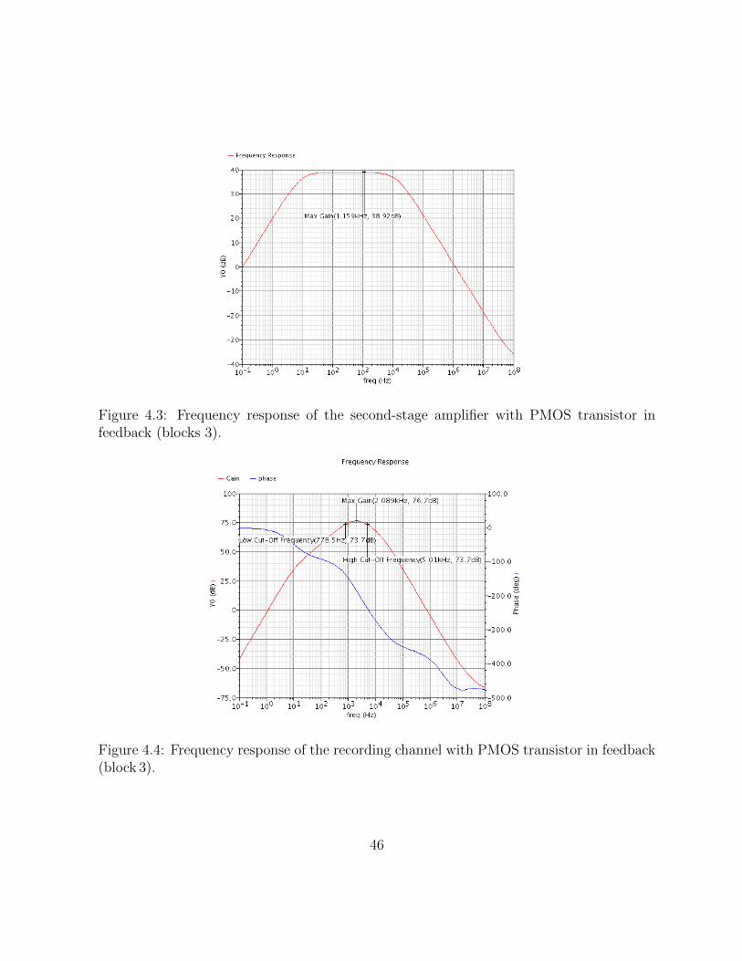
Gain is an important factor in the design of second-stage amplifiers. In our design, we
set the gain of the second-stage amplifier to 40 dB. Figure 4.3 shows the frequency response
of the fully differential amplifier with PMOS transistors in feedback. It can be seen that
the gain is 38.92 dB.
Figure 4.1 shows the AC simulation of the whole recording channel for the fully dif-
ferential amplifiers with PMOS transistors in feedback. The total gain of the channel is
76.7 dB, and the low and high corner frequencies of the channel are 778 Hz and 5 kHz,
respectively. The input-referred noise of the recording channel integrating from 0.1 Hz to 1
45
Figure 4.3: Frequency response of the second-stage amplifier with PMOS transistor infeedback (blocks 3).
Figure 4.4: Frequency response of the recording channel with PMOS transistor in feedback(block 3).
46
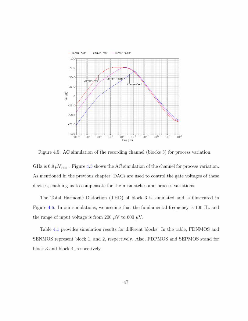
Figure 4.5: AC simulation of the recording channel (blocks 3) for process variation.
GHz is 6.9µVrms . Figure 4.5 shows the AC simulation of the channel for process variation.
As mentioned in the previous chapter, DACs are used to control the gate voltages of these
devices, enabling us to compensate for the mismatches and process variations.
The Total Harmonic Distortion (THD) of block 3 is simulated and is illustrated in
Figure 4.6. In our simulations, we assume that the fundamental frequency is 100 Hz and
the range of input voltage is from 200 µV to 600 µV.
Table 4.1 provides simulation results for different blocks. In the table, FDNMOS and
SENMOS represent block 1, and 2, respectively. Also, FDPMOS and SEPMOS stand for
block 3 and block 4, respectively.
47
Figure 4.6: Simulated total harmonic distortion of recording channel (block 3) with a inputvoltage varies from 200 µV to 600 µV
Table 4.1: Simulation results for different blocks.Block Gain (dB) Noise (µVrms) Power Dissipation (µW) THD @ 200 µV (%)
FDNMOS (1) 77.55 6.9 150 11.31SENMOS (2) 77.4 7.2 125 15.59FDPMOS (3) 76.7 6.9 150 2.76SEPMOS (4) 77.3 7.2 125 2.6
48
Figure 4.7: Die Photo of 16-channel neural recording
4.2 Design of AF5 PCB
The AF5 analog front-end was fabricated in AMS 0.35 µm CMOS technology. Figure 4.7
shows a die photo of the AF5 chip.
A four-layer PCB (AF5PCB) using Altium software was designed to test the chip, and
is shown in Figure 4.8. The two inner layers are used for the ground and power supply.
Each layer is also split into analog and digital sides for high-speed performance and the
noise reduction. The PCB has four separate 3.3V regulators for analog supply of the board,
analog supply of the AF5 chip, the digital supply of the board and digital supply of the
AF5 chip.
49
Figure 4.8: AF5PCB board
The chip must be tested with a simple signal generator before live recordings. To
simulate neural signals, we need to attenuate the outputs of signal generators as the real
neural signals have very small amplitude. Thus, a simple resistor divider is used. The
resistor values were chosen so as to imitate the electrodes’ impedance. A capacitor is placed
parallel to the outputs of resistor dividers to filter excess noise. To use the input signals
coming from electrodes in live recording, the PCB includes a connector for interfacing
with the Cerebus, which is a commercial system for recording and analysing the nervous
network of animals brain [57]. Thus, the board can be used in live experiments.
An Opal-Kelly XEM6010 board with XC6SLX45 Xilinx FPGA is used to provide the
digital data needed for the digital part of the chip as well as for getting the digital output
data of the AF5. The DC voltages required by by DACs and CMFB circuits in the chip
are provided by either the digital or analog potentiometer (POT). The output signals of
50
the recording channels in the chip are connected to the MUXs in the PCB. If a digital
output signal is needed, then the MUX’s output can be connected to a buffer and then
an ADC. The digital output of the ADC is then connected to the Opal-Kelly module for
signal processing.
4.3 Test Results
The first step in testing the chip is to provide the required digital data for the shift-registers
in the chip. A code was written for the Opal-Kelly module and then loaded into it. The
Opal-Kelly sends the data to the chip. Measurements show that the output signal of serial
shift register is similar to the input signal of that, but with a delay, and so the digital part
of the chip works correctly.
Next, we program the chip to test the recording channels. Figure 4.9 illustrates the
output signals of the LNA for a 3 mV input signal at 1 kHz frequency. It can be seen that
the LNA has a gain of 34.9 dB. The outputs of the recording channels were also probed.
Figure 4.10 shows the output signals of a fully differential recording channel with PMOS
in feedback (block 3), with an input signal of 200µV at 1 kHz frequency.
It was mentioned that the DACs were used to control the channels’ frequency response
by controlling the transistors’ gate voltages. The frequency response of the LNA with
different DAC values is demonstrated in Figure 4.11, and it confirms that the channels
work as expected.
Figure 4.12 demonstrates the measured noise of channel 10 in the range of frequency
51
Figure 4.9: Output signal of the LNA with PMOS in feedback (channel 10).
Figure 4.10: Output signals of a fully differential recording channel with PMOS in feedback(channel 10).
52
Figure 4.11: Measured frequency response of the LNA with PMOS in feedback (channel10) with different DAC values.
from 1 Hz to 50 kHz. By using this, the input referred noise integrated from 1 Hz to 50 kHz
equals 1.4 mV. Unfortunately, the noise of the testing board is much higher than the chip
noise, and thus the measured input referred noise is mainly due to noise of the board.
The power consumption of the chip is 2.7 mW, which is close to the simulation result
(2.6 mW).
Table 4.2 shows that what channels are functional in our experiments, and Table 4.3
provides the test results of different parameters for the working blocks. An overall summary
on our chip and its characteristics is given in Table 4.4.
53
Figure 4.12: Measured noise of recording channel for block 10
Table 4.2: Functionality of different recording channels
Block Channel NO. Tested Functional Low cut-off FrequencyFDNMOS (1) 1 Y NO -FDNMOS (1) 2 Y NO -FDNMOS (1) 3 Y NO -FDNMOS (1) 4 Y NO -SENMOS (2) 5 Y NO -SENMOS (2) 6 Y NO -SENMOS (2) 7 Y NO -SENMOS (2) 8 Y Y 0.1 Hz to 600 HZFDPMOS (3) 9 Y NO -FDPMOS (3) 10 Y Y 0.1 Hz to 1kHZFDPMOS (3) 11 Y Y 0.1 Hz to 1kHZFDPMOS (3) 12 Y Y 0.1 Hz to 1kHZSEPMOS (4) 13 Y Y 0.1 Hz to 1kHZSEPMOS (4) 14 Y Y 0.1 Hz to 1kHZSEPMOS (4) 15 Y NO -SEPMOS (4) 16 Y NO -
54
Table 4.3: Test and Simulation results for different blocksTest Results Simulation Results
Block Gain (dB) THD @ 200µ (%) Gain (dB) THD @ 200µ (%)SENMOS(2) 74.7 9.4 77.4 15.5FDPMOS(3) 77.5 3.76 76.7 2.76SEPMOS(4) 71.2 1.9 77.3 2.6
Table 4.4: Measurement results of the AF5 chip
Number of Channels 16Gain 77.5 dB
Power Supply 3.3VLow cut-off Frequency Adjustable from 0.1 Hz to 1kHZHigh cut-off Frequency 2.5 kHzTotal Power Dissipation 2.7 mW
Chip Area 3 mm × 3 mmTechnology 0.35µm
55
Chapter 5
Conclusions
5.1 Summary of the Work and Contributions
This work focuses on the design and implementation of a field-programmable 16-channel
analog front-end for the neural recording systems. Each recording channel contains two-
stage amplifiers, as well as DACs, which are used for controlling the low corner frequency
response of each channel digitally to overcome process variation, and other mismatches.
The circuits of the chip are designed for good noise performance and power consumption.
The 16 recording channels are divided into four different blocks to evaluate the per-
formances of different architectures. The first block includes one LNA as the first stage
amplifier and a fully differential amplifier as the second stage. An NMOS transistor is used
in the feedback loop of the amplifier. Block 2 uses a single-ended amplifier instead of the
fully differential amplifier as a second stage. Block 3 and 4 are similar to blocks 1 and 2,
56
respectively, with small differences where blocks 3 and 4 use two PMOS in series instead
of an NMOS transistor in feedback.
Neural recording systems should be fully implantable, and thus they need to be tuned
automatically. This chip is programmable so that we can ultimately implement a self-
tuning feature on chip. We aim to digitally tune the frequency response of the channels
with the aid of DACs. Specifically, there exist FPGA and ADCS on the board to drive the
DACs for the purpose of self-tuning.
The chip is fabricated in AMS 0.35 CMOS technology and is tested on an AF5PCB
board, which was designed for this purpose. The board has the ability to be used for
in-vivo recording. Unfortunately, in-vivo testing could not be done due to the limited time
available. However, our clinical colleagues in Alberta will start live testing in the near
future.
5.2 Future Work
• Four different architectures have been used in the design of our recording channels.
These architectures will be evaluated and compared completely in in-vivo testing,
and the best architecture will be chosen for future designs.
• A better understanding of how each circuit works in the chip may be obtained after
testing the chip. This knowledge can be used in designing different circuits for the
next chip. As an example, the transistors’ sizing can be changed so as to be optimized
for design specifications.
57
• Although the chip and the board are designed to provide the circuits required to
perform self-tuning feature, this feature was not implemented because of limited
time. The algorithms needed to evaluate this feature will be implemented in the
near future.
• In order to have all the systems on our chip and have a fully-implantable device,
the on-chip analog-to-digital converter and the circuitry for sensing the frequency
response will be included in the next chip.
58
Appendix A
Current and Voltage Reference
A.1 Design of Current Reference
The current and voltage references are among the most important blocks in every design,
as they provide biasing voltages for the circuits. An ideal voltage reference block should
be independent of any fluctuations in power supply and temperature.
Using bipolar transistors, the band-gap circuits are designed to make stable and reli-
able reference voltages. However, the architecture is not preferred in our design since its
implementation by CMOS technology is cumbersome. Therefore, we use a beta multiplier
reference (BMR) suggested in [6] for CMOS technology. Figure A.1 shows a schematic for
this circuit with its start-up circuit. Table A.1 shows the transistor sizing for the BMR
circuit.
In this circuit the W/L ratio of transistors M3 and M4 are equal, so they have the same
60
VDD VDD VDD VDD
M4
M2
M3
M1
M5
M7
M6
R1
VREF
IREFStart-Up
Figure A.1: Schematic of Beta multiplier reference circuit
current for each branch. We have
VGS1 = VGS2 + IREF .R1 , (A.1)
where VGS is the voltage between the gate and source of the transistor. To ensure that the
circuit works correctly, VGS1 should be greater than VGS2. This condition is satisfied by
making the W of transistor M2, K time larger than that of M1, while K is greater than 1.
Furthermore, K greater than 1 guarantees positive feedback in the circuit, resulting in a
stable circuit. Using Eq. A.1 and the current equations of transistor M1 and M2, we can
derive the IREF and VREF values as below
IREF =2
R21KµnCOX
W1
L1
(1− 1√K
) , (A.2)
61
Table A.1: Transistor sizing of BMR circuit.
Transistor W/L(µm)M1 2/2M2,3,4 4* 2/2M5 2/1M6 1/80M7 2* 4/1
VREF =2
R1KµnCOXW1
L1
(1− 1√K
) + Vthn , (A.3)
where Vthn is the threshold voltage of the NMOS transistor. It can be seen that both VREF
and IREF values are independent of power supply.
Since the resistor, R1, has a positive temperature coefficient, a rise of temperature in-
creases the voltage drop across R1. On the other hand, VGS2 has an inverse response since
Vth has negative temperature coefficients. In other words, increasing the temperature re-
duces VGS. Therefore, by finding a proper value for R1, these two voltages can compensate
for each other and produce a voltage that is not a function of temperature [35]. Eq. A.4
and A.5 show the temperature coefficients of IREF and VREF , respectively.
∂IREF
∂T= IREF .[
−2
R1
∂R1
∂T− 1
KµnCOX
∂KµnCOX
∂T)] , (A.4)
∂VREF
∂T=∂Vthn∂T
− 2
R1KµnCOXW1
L1
(1− 1√K
).(1
R1
∂R1
∂T+
1
KµnCOX
∂KµnCOX
∂T) . (A.5)
62
It can be concluded from the equation that the IREF and VREF temperature coefficients
depend on W/L, R1 and K, and so proper values for these parameters results in the desired
reference values. The K value is set to 4 in most designs, and is called a constant-gm bias
circuit. By choosing K=4, gm is equal to A.6. It can be seen that, gm is not a function of
MOSFET process shifts, and is a constant value [6].
gm =
√2KµnCOX
W1
L1
.IREF =1
R1
(A.6)
The BMR circuit is a self-biased circuit, and so it is essential to use a start-up circuit
that prevents circuits working at zero current values. If a circuit works in this situation,
transistors M1-M4 are off at time zero. The voltage gate of M1 and M2 is zero, while
the voltage at the gate of M3 and M4 is VDD, causing M7 and then M6 to be turned off.
Consequently, the gate-source voltage of M6 is less than Vthn, causing M5 to be ON, which
runs the current flow through M1 and M2. The voltage of gate M1 and M2 keeps increasing
until all 4 transistors are ON. When the circuit works at the desired biasing points, M6
turns OFF.
As seen in previous sections, different biasing voltages are needed to bias the telescopic
and Folded-Cascode amplifiers. The circuit shown in Figure A.2 is used to provide the
required voltages for both amplifiers [6]. Since the bias voltages are different for these
amplifiers, the sizing of transistors for each amplifier is different, to reach the desired bias
voltages. Tables A.2 and A.3 show the transistor sizing for the telescopic and folded-
Cascode amplifiers, respectively.
63
VDD
VDD VDD VDD
VBIAS1
VBIAS3
VBIASN
VBIAS2
VBIAS4
M1
M2 M5
M4
M3 M6
M7
M8
M9
M10
M11
M12
Figure A.2: Schematic of biasing circuit for telescopic and folded-cascode amplifier
Table A.2: Transistor sizing of LNA-biasing
Transistor W/L(µm)M1 1/16M2,5 2/2M3,6,9 8/10M4,7,10 4/1M8 1/40M11 1/1M12 2/10
Table A.3: Transistor sizing of folded-cascode biasing
Transistor W/L(µm)M1 4/20M2,5 1/1M3,6,9 4/1M4,7,10 4/1M8 1/20M11,12 1/1
64
A.2 Simulation and Test Results
The VREF of BMR circuit as well as the 4 VBIAS voltages provided for each amplifier
should be probed to ensure the circuit is biased at the preferred bias points. The VREF
is connected directly to the output pad. The 8 VBIAS points for each amplifier stage were
connected to an 8×1 MUX, while the output of the MUX is connected to one output
pad. The reference and biasing voltages were probed. Table A.4 shows the simulation and
measurement results of these testing points. It can be seen that the measured value of
voltages are close to what we expected from simulation.
Table A.4: Simulation and test results of biasing voltages
Biasing Voltage Simulations MeasurementsVREF 0.673 0.67
V BIASL1 2.298 2.22V BIASL2 1.298 1.27V BIASL3 1.709 1.56V BIASL4 0.891 0.88V BIASF1 2.439 2.42V BIASF2 1.984 1.92V BIASF3 1.308 1.15V BIASF4 0.678 0.67
65
Appendix B
Simulation Results of Other Blocks
The simulation results of block 3 was shown in chapter 4. The simulation results of the
other blocks are presented here. Figure B.1, B.2 and B.3 show the AC simulation of blocks
1, 2, 4, respectively. Figure B.4 shows the simulated THD for each block.
66
Figure B.1: Frequency response of the recording channels for block 1
Figure B.2: Frequency response of the recording channels for block 2
67
References
[1] T. Akin, K. Najafi, and R. M. Bradley. A wireless implantable multichannel digitalneural recording system for a micromachined sieve electrode. IEEE Journal of Solid-State Circuits, 33(1):109–118, 1998.
[2] P. E. Allen and D. R. Holberg. CMOS analog circuit design. Oxford University Press,second edition, 2002.
[3] B. Aouizerate, E. Cuny, C. Martin-Guehl, D. Guehl, H. Amieva, A. Benazzouz, C. Fab-rigoule, M. Allard, A. Rougier, B. Bioulac, J. Tignol, and P. Burbaud. Deep brainstimulation of the ventral caudate nucleus in the treatment of obsessive-compulsivedisorder and major depression: Case report. Journal of neurosurgery, 101(4):682–686,2004.
[4] M. A. Arbib. The handbook of brain theory and neural networks. MIT Press, secondedition, 2003.
[5] J. N. Y. Aziz, R. Genov, B. L. Bardakjian, M. Derchansky, and P. L. Carlen. Brain-silicon interface for high-resolution in vitro neural recording. IEEE Transactions onBiomedical Circuits and Systems, 1(1):56–62, 2007.
[6] R. J. Baker. CMOS: Circuit Design, Layout, and Simulation: Third Edition. JohnWiley & Sons, 2011.
[7] M. Banu, J. M. Khoury, and Y. Tsividis. Fully differential operational amplifiers withaccurate output balancing. IEEE Journal of Solid-State Circuits, 23(6):1410–1414,1988.
[8] M. W. Barnett and P. M. Larkman. The action potential. Practical Neurology,7(3):192–197, 2007.
70
[9] A. Bernyi, M. Belluscio, D. Mao, and G. Buzski. Closed-loop control of epilepsy bytranscranial electrical stimulation. Science, 337(6095):735–737, 2012.
[10] A. Borna, T. Marzullob, G. Gage, and K. Najafi. A small, light-weight, low-power,multichannel wireless neural recording microsystem. Conference proceedings : An-nual International Conference of the IEEE Engineering in Medicine and Biology So-ciety.IEEE Engineering in Medicine and Biology Society.Conference, 2009:5413–5416,2009.
[11] T. C. Carusone, D. A. Johns, and K. W. Martin. Analog integrated circuit design.John Wiley & Sons, second edition, 2012.
[12] M. S. Chae, W. Liu, and M. Sivaprakasam. Design optimization for integrated neuralrecording systems. IEEE Journal of Solid-State Circuits, 43(9):1931–1939, 2008.
[13] J. K. Chapin, K. A. Moxon, R. S. Markowitz, and M. A. L. Nicolelis. Real-time controlof a robot arm using simultaneously recorded neurons in the motor cortex. Natureneuroscience, 2(7):664–670, 1999.
[14] C. T. Charles. Wireless data links for biomedical implants: Current research andfuture directions. In Conference Proceedings - IEEE Biomedical Circuits and SystemsConference Healthcare Technology, BiOCAS2007, pages 13–16, 2007.
[15] O. Devinsky. Patients with refractory seizures. New England Journal of Medicine,340(20):1565–1570, 1999.
[16] D. M. Di Pietro and J. D. Meindl. Optimal system design for an implantablecw doppler ultrasonic flowmeter. IEEE Transactions on Biomedical Engineering,25(3):255–264, 1978.
[17] H. Eichenbaum, D. Pettijohn, A. M. Deluca, and S. L. Chorover. Compact miniaturemicroelectrode-telemetry system. Physiology and Behavior, 18(6):1175–1178, 1977.
[18] C. D. Ferris. Introduction to bioinstrumentation : with biological, environmental, andmedical applications. Humana Press, 1978.
[19] T. B. Fryer, H. Sandler, W. Freund, E. P. McCutcheon, and E. L. Carlson. A mul-tichannel implantable telemetry system for flow, pressure, and ecg measurements.Journal of applied physiology, 39(2):318–326, 1975.
[20] P. R. Gigante and R. R. Goodman. Alternative surgical approaches in epilepsy. Cur-rent Neurology and Neuroscience Reports, 11(4):404–408, 2011.
71
[21] P. R. Gray, P. J. Hurst, S. H. Lewis, and R. G. Meyer. Analysis and design of analogintegrated circuits. Wiley, 5th edition, 2009.
[22] R. Harrison, P. Watkins, R. Kier, R. Lovejoy, D. Black, R. Normann, andF. Solzbacher. A low-power integrated circuit for a wireless 100-electrode neuralrecording system. In Digest of Technical Papers - IEEE International Solid-StateCircuits Conference, 2006.
[23] R. R. Harrison. A versatile integrated circuit for the acquisition of biopotentials. InProceedings of the Custom Integrated Circuits Conference, pages 115–122, 2007.
[24] R. R. Harrison and C. Charles. A low-power, low-noise cmos amplifier for neuralrecording application. IEEE Journal of Solid-State Circuits, 38(6):958–965, 2003.
[25] R. R. Harrison, R. J. Kier, C. A. Chestek, V. Gilja, P. Nuyujukian, S. Ryu, B. Greger,F. Solzbacher, and K. V. Shenoy. Wireless neural recording with single low-power inte-grated circuit. IEEE Transactions on Neural Systems and Rehabilitation Engineering,17(4):322–329, 2009.
[26] R. R. Harrison, P. T. Watkins, R. J. Kier, R. O. Lovejoy, D. J. Black, B. Greger,and F. Solzbacher. A low-power integrated circuit for a wireless 100-electrode neuralrecording system. IEEE Journal of Solid-State Circuits, 42(1):123–133, 2007.
[27] B. Hille. Ion Channels of Excitable Membranes. Sinauer Associates, Sunder-land,Massachusetts, 2001.
[28] L. R. Hochberg, M. D. Serruya, G. M. Friehs, J. A. Mukand, M. Saleh, A. H. Caplan,A. Branner, D. Chen, R. D. Penn, and J. P. Donoghue. Neuronal ensemble control ofprosthetic devices by a human with tetraplegia. Nature, 442(7099):164–171, 2006.
[29] A. L. Hodgkin and A. F. Huxley. A quantitative description of membrane currentand its application to conduction and excitation in nerve. The Journal of physiology,117(4):500–544, 1952.
[30] J. Ji and K. D. Wise. An implantable cmos circuit interface for multiplexed mi-croelectrode recording arrays. IEEE Journal of Solid-State Circuits, 27(3):433–443,1992.
[31] S. Kim, R. A. Normann, R. Harrison, and F. Solzbacher. Preliminary study of the ther-mal impact of a microelectrode array implanted in the brain. In Proc. Annual Inter-national Conference of the IEEE Engineering in Medicine and Biology Society.IEEEEngineering in Medicine and Biology Society.Conference, 1:2986–2989, 2006.
72
[32] A. E. Lang and A. J. Lees. Management of parkinson’s disease: An evidence-basedreview. Movement Disorders, 17(SUPPL. 4), 2002.
[33] M. A. Lebedev and M. A. L. Nicolelis. Brain-machine interfaces: past, present andfuture. Trends in neurosciences, 29(9):536–546, 2006.
[34] H. Li. A neural recording front end for multi-channel wireless implantable applications.Master’s thesis, Michigan State University, 2011.
[35] S. Liu and R.J. Baker. Process and temperature performance of a cmos beta-multipliervoltage reference. in Proc. IEEE Int. Midwest Symp.Circuits and Systems (MWS-CAS), pages 33–36, 1998.
[36] W. Liu, M. Sivaprakasam, W. Gang, and S. C. Moo. A neural recording systemfor monitoring shark behavior. In Proceedings - IEEE International Symposium onCircuits and Systems, pages 4123–4126, 2006.
[37] Y. Lo, W. Liu, K. Chen, M. . Tsai, and F. Hsueh. A 64-channel neuron recording sys-tem. In Proceedings of the Annual International Conference of the IEEE Engineeringin Medicine and Biology Society, EMBS, pages 2862–2865, 2011.
[38] F. Maloberti. Data Converters. Springer, 2007.
[39] K. Najafi and K. D. Wise. An implantable multielectrode array with on-chip signalprocessing. IEEE Journal of Solid-State Circuits, SC-21(6):1035–1044, 1986.
[40] A. K. Ngugi, C. Bottomley, I. Kleinschmidt, J. W. Sander, and C. R. Newton. Es-timation of the burden of active and life-time epilepsy: A meta-analytic approach.Epilepsia, 51(5):883–890, 2010.
[41] C. T. Nordhausen, E. M. Maynard, and R. A. Normann. Single unit recording capa-bilities of a 100 microelectrode array. Brain research, 726(1-2):129–140, 1996.
[42] R. H. Olsson, M. N. Gulari, and K. D. Wise. A fully-integrated bandpass amplifierfor extracellular neural recording. Proc.1st Int.IEEE EMBS Conf.Neural Engineering,pages 165–168, 2003.
[43] P. G. Patil and D. A. Turner. The development of brain-machine interface neuropros-thetic devices. Neurotherapeutics, 5(1):137–146, 2008.
73
[44] G. E. Perlin and K. D. Wise. An ultra compact integrated front end for wireless neuralrecording microsystems. Journal of Microelectromechanical Systems, 19(6):1409–1421,2010.
[45] K. G. Plass. A new ultrasonic flowmeter for intravascular application. IEEE Trans-actions on Biomedical Engineering, 11(4):154–156, 1964.
[46] D. Purves, G. J. Augustine, D. Fitzpatrick, L. C. Katz, A. LaMantia, J. O. McNamara,and S. M. Williams. Neuroscience. Sinauer Associates, Sunderland,Massachusetts,second edition, 2001.
[47] R. D. Rader, J. P. Meehan, and J. K. C. Henriksen. An implantable blood pressure andflow transmitter. IEEE Transactions on Biomedical Engineering, BME-20(1):37–43,1973.
[48] B. Razavi. Design of Analog CMOS Integrated Circuits. McGraw-Hill, 2001.
[49] H. Sandler, T. B. Fryer, and B. Datnow. Single-channel pressure telemetry unit.Journal of applied physiology, 26(2):235–238, 1969.
[50] T. M. Seese, H. Harasaki, G. M. Saidel, and C. R. Davies. Characterization of tissuemorphology, angiogenesis, and temperature in the adaptive response of muscle tissueto chronic heating. Laboratory Investigation, 78(12):1553–1562, 1998.
[51] R. Shulyzki, K. Abdelhalim, A. Bagheri, C. M. Florez, P. L. Carlen, and R. Genov.256-site active neural probe and 64-channel responsive cortical stimulator. In Proceed-ings of the Custom Integrated Circuits Conference, 2011.
[52] A. M. Sodagar and K. Najafi. Wireless interfaces for implantable biomedical microsys-tems. In Midwest Symposium on Circuits and Systems, volume 2, pages 265–269, 2006.
[53] A. M. Sodagar, G. E. Perlin, Y. Yao, K. Najafi, and K. D. Wise. An implantable64-channel wireless microsystem for single-unit neural recording. IEEE Journal ofSolid-State Circuits, 44(9):2591–2604, 2009.
[54] D. M. Taylor, S. I. H. Tillery, and A. B. Schwartz. Direct cortical control of 3dneuroprosthetic devices. Science, 296(5574):1829–1832, 2002.
[55] G. Wang. An Integrated, Low Noise Neural Recording System. PhD thesis, UniversityOf California Santa Cruz, 2009.
74
[56] P. T. Watkins, R. J. Kier, R. O. Lovejoy, D. J. Black, and R. R. Harrison. Signalamplification, detection and transmission in a wireless 100-electrode neural recordingsystem. In Proceedings - IEEE International Symposium on Circuits and Systems,pages 2193–2196, 2006.
[57] Cerberus website. http://www.blackrockmicro.com/content.aspx?id=13.
[58] J. G. Webster. Bioinstrumentation. John Wiley & Sons, 2004.
[59] R. Wertz, G. Maeda, and T. J. Willey. Design for a micropowered multichannelpam/fm biotelemetry system for brain research. Journal of applied physiology, 41(5),1976.
[60] J. Wessberg, C. R. Stambaugh, J. D. Kralik, P. D. Beck, M. Laubach, J. K. Chapin,J. Kim, S. J. Biggs, M. A. Srinivasan, and M. A. L. Nicolelis. Real-time prediction ofhand trajectory by ensembles of cortical neurons in primates. Nature, 408(6810):361–365, 2000.
[61] D. Money Weste, N. H. E. Harris. CMOS VLSI design : a circuits and systemsperspective. Addison-Wesley, 4th edition, 2011.
[62] Y. Yonezawa, I. Ninomiya, and N. Nishiura. A multichannel telemetry systemfor recording cardiovascular neural signals. The American Journal of Physiology,236(3):H513–518, 1979.
75