Journal of Multidisciplinary Engineering Science and Technology (JMEST) ISSN: 2458-9403 Vol. 4 Issue 4, April - 2017 www.jmest.org JMESTN42352133 7026 Design And Simulation Of Amplitude Modulation Network For Analog Communication Systems 1 Assistant prof. Dr.Haitham K.Ali, Sulaimani polytechnic university Technical college of engineering, Sulaimani, Kurdistan Region, Iraq ([email protected] ) +964-7703606127 2 Jihan S. Abdoljabar Sulaimani polytechnic university Technic of engineering, Sulaimani, Kurdistan Region, ([email protected]) +964- 07702206886 Abstract—With the increasing demand in communication, a tremendous technological transformation during the last two decades has provided a potential growth in the area of digital communication and lot of newer applications and technologies are coming up every day due to these reasons. Restricting over self to the domain of modulation techniques a brief overview and design over an analog modulation technique has been provided in this article through extensive literature survey in a tabular manner enabling to analyze and establish the superiority at a glance of a specific modulation technique for a particular application. At this paper the design of AM modulation network was designed and it is consist of three important units which are the Audio signal oscillator, the RF signal oscillator and the AM modulator (Multiplier). The total system was connected together and the output was measured at each part of the system and the output Am wave of the total system was 100% the same as the wave of the ideal AM wave moreover the output at each part was measured and the results were acceptable comparing with the ideal results . These blocks were designed using multisim software (version12). Keywords—AM modulation, mutism software, Multiplier, RF signal I. Introduction Amplitude modulation (AM) is a technique used in electronic communication, most commonly for transmitting information via a radio carrier wave. The AM works by varying the strength of the transmitted signal in relation to the information being sent. For example, changes in the signal strength can be used to reflect the sounds to be reproduced by a speaker, or to specify the light intensity of television pixels. Contrast this with frequency modulation, also commonly used for sound transmissions, in which the frequency is varied.An important consideration in amplitude modulation is to describe the depth of modulation i.e. the extent to which the amplitude of carrier wave is changed by the signal. This is described by a factor called modulation factor which may be defined as under: The ratio of change of amplitude of carrier wave to the amplitude of normal carrier wave is called the Modulation factor. There are basically three types of analog modulation schemes the amplitude modulation, the Frequency modulation and the phase modulation schemes which have in turn lot of class[1]. In case of the Amplitude Modulation there are several derivatives and it is evident from the comparative the Single Side Band Suppressed Carrier (SSS-SC) has smaller bandwidth be better than other AM schemes but practically, VSB proves to be a much better candidate then the other amplitude modulation techniques.The Amplitude modulated signals require nonlinear amplifiers which generate spurious out-of-band spectral components which are filtered out with a great difficulty. Frequency Modulation proves to be better in comparison to amplitude modulation and phase modulation, and the derivative of frequency modulation, narrow band FM (NBFM) is usually employed to overcome above mentioned problems in the communication system. The major limitation of the analog modulation systems for communicating over long channels is that once noise has been introduced at any place along the channel, then it is carried out till the end. Because the analog modulation system (AM, FM and PM ) are extremely sensitive to the noise present at the receiver end in contrast to this if a digital signal is modulated and transmitted the received signal is far less sensitive to receiver.[2] II. Application of AM modulator 1. Amplitude modulation sound, so called swish sound, is generally contained in wind turbine noise (WTN) and it causes serious annoyance in the areas around wind farms. Therefore, the methods to assess the characteristics of this kind of sound should be investigated in both viewpoints, physically and psycho-acoustically. Regarding the former problem, a practical method to evaluate the magnitude of the AM
Transcript
Journal of Multidisciplinary Engineering Science and Technology (JMEST) ISSN: 2458-9403
Vol. 4 Issue 4, April - 2017
www.jmest.org
JMESTN42352133 7026
Design And Simulation Of Amplitude Modulation Network For Analog Communication
Systems
1Assistant prof. Dr.Haitham K.Ali,
Sulaimani polytechnic university
Technical college of engineering, Sulaimani, Kurdistan Region, Iraq
Abstract—With the increasing demand in communication, a tremendous technological transformation during the last two decades has provided a potential growth in the area of digital communication and lot of newer applications and technologies are coming up every day due to these reasons. Restricting over self to the domain of modulation techniques a brief overview and design over an analog modulation technique has been provided in this article through extensive literature survey in a tabular manner enabling to analyze and establish the superiority at a glance of a specific modulation technique for a particular application. At this paper the design of AM modulation network was designed and it is consist of three important units which are the Audio signal oscillator, the RF signal oscillator and the AM modulator (Multiplier). The total system was connected together and the output was measured at each part of the system and the output Am wave of the total system was 100% the same as the wave of the ideal AM wave moreover the output at each part was measured and the results were acceptable comparing with the ideal results . These blocks were designed using multisim software (version12).
Keywords—AM modulation, mutism software, Multiplier, RF signal
I. Introduction
Amplitude modulation (AM) is a technique used in electronic communication, most commonly for transmitting information via a radio carrier wave. The AM works by varying the strength of the transmitted signal in relation to the information being sent. For example, changes in the signal strength can be used to reflect the sounds to be reproduced by a speaker, or to specify the light intensity of television pixels. Contrast this with frequency modulation, also commonly used for sound transmissions, in which the frequency is varied.An important
consideration in amplitude modulation is to describe the depth of modulation i.e. the extent to which the amplitude of carrier wave is changed by the signal. This is described by a factor called modulation factor which may be defined as under: The ratio of change of amplitude of carrier wave to the amplitude of normal carrier wave is called the Modulation factor. There are basically three types of analog modulation schemes the amplitude modulation, the Frequency modulation and the phase modulation schemes which have in turn lot of class[1]. In case of the Amplitude Modulation there are several derivatives and it is evident from the comparative the Single Side Band Suppressed Carrier (SSS-SC) has smaller bandwidth be better than other AM schemes but practically, VSB proves to be a much better candidate then the other amplitude modulation techniques.The Amplitude modulated signals require nonlinear amplifiers which generate spurious out-of-band spectral components which are filtered out with a great difficulty. Frequency Modulation proves to be better in comparison to amplitude modulation and phase modulation, and the derivative of frequency modulation, narrow band FM (NBFM) is usually employed to overcome above mentioned problems in the communication system. The major limitation of the analog modulation systems for communicating over long channels is that once noise has been introduced at any place along the channel, then it is carried out till the end. Because the analog modulation system (AM, FM and PM ) are extremely sensitive to the noise present at the receiver end in contrast to this if a digital signal is modulated and transmitted the received signal is far less sensitive to receiver.[2]
II. Application of AM modulator
1. Amplitude modulation sound, so called swish sound, is generally contained in wind turbine noise (WTN) and it causes serious annoyance in the areas around wind farms. Therefore, the methods to assess the characteristics of this kind of sound should be investigated in both viewpoints, physically and psycho-acoustically. Regarding the former problem, a practical method to evaluate the magnitude of the AM
Journal of Multidisciplinary Engineering Science and Technology (JMEST) ISSN: 2458-9403
Vol. 4 Issue 4, April - 2017
www.jmest.org
JMESTN42352133 7027
using common acoustic measurement instrumentation is proposed in this paper. That is, the sound pressure level difference between the levels measured by using FAST and SLOW dynamic characteristics of a sound level meter is calculated for the measurement time interval under investigation and then the cumulative distribution function of the level difference is calculated. From the result, the value of 90% range is obtained as an indicator for assessing the AM. Statistical data evaluated by using this indicator for AM sounds contained in actual WTNs were obtained through the field measurements performed nationwide across Japan. [3]
2. Results of two channel simultaneous audio recordings outdoors in the free field and inside a bedroom are presented from the Leonards Hill wind farm that has two Repower 2MW MM82 wind turbines. The analysis demonstrates the dynamic effects of amplitude modulation on attenuation of sound between the two measurement locations and shows how outdoor to indoor attenuation is compromised at particular room resonant modes. Different measurement approaches are discussed with the conclusion that a 10Hz sampling rate of sound level is insufficient to accurately determine peak to trough amplitude modulations. Infrasound measurements are also presented to show that amplitude modulation is also observable below 20Hz and that low frequency infrasound may also be considered to be amplitude modulation. [4]
3. This application proposes a data hiding scheme for amplitude-modulation (AM) radio broadcasting systems. The method of digital audio watermarking based on cochlear delay (CD) that we previously proposed is employed in this scheme to construct a data hiding scheme in the AM domain. We investigate the feasibility of applying the method of CD-based inaudible watermarking to send inaudible additional messages in AM signals. The proposed scheme modulates a carrier signal with both original and watermarked signals as lower and upper sidebands by using the novel double-modulation and then transmits the modulated signal to the receivers. Particular receivers in the proposed scheme demodulate the received signals to get both original and watermarked signals by using the double-demodulation and then extract messages from the watermarked signal and the original signal using CD-based watermarking. The results we obtained from computer simulations revealed that the proposed scheme can transmit messages as watermarks in AM signals and then correctly extract the messages from observed AM signals. The results also indicated that the sound quality of the demodulated signals could be kept high not only with the proposed scheme but also in traditional AM radio systems. This means that the proposed scheme has the possibility of acting as a hidden-message transmitter as well as having low-level compatibility with AM radio systems. The proposed scheme could be applied in emergency alert systems and high utility AM radio services. [5]
4. Recovery and analysis of the 1st harmonic signals in tunable diode laser spectroscopy (TDLS) with wavelength modulation (WM) are limited by the presence of a high background signal upon which the small gas signals are superimposed. This high background signal is a result of direct modulation of the source laser power and is referred to as the residual amplitude modulation (RAM) signal. This paper presents further details of a recently reported technique to optically remove the RAM and an analytical model that enables the use of the phasor decomposition (PD) method with it to extract the absolute gas absorption lineshape from the recovered 1st harmonic signals. The PD method is important as it provides a calibration-free technique for gas concentration measurements. A major benefit of RAM nulling is that signal amplification can be increased without equipment saturation due to the background RAM, resulting in improved signal resolution and system sensitivity. A comparison of experimental measurements of the 1650.96nm absorption line of methane (CH4) with lineshapes derived from HITRAN data illustrates and validates the use of the PD method with the new RAM nulling procedure. This advancement is useful for industrial applications where stand-alone and calibration-free instrumentation is required. Tunable diode laser spectroscopy with wavelength modulation: Elimination of residual amplitude modulation in a phasor decomposition approach.[6]
III. SIMULATION AND DESIGN OF AM BLOCKS
In order to design the AM modulator we need to build three important parts which represent by: the Audio signal oscillator, the RF signal oscillator and the AM modulator (Multiplier) as shown in figure (1).
Figure (1): AM Block Diagram
A. Analog Multiplier Design
An analog multiplier is a device having two input ports and an output port. The signal at the output is the product of the two input signals. If both input and output signals are voltages, the transfer characteristic is the product of the two input voltages divided by a scaling factor K. The multiplier block diagram is shown in figure (2)
Journal of Multidisciplinary Engineering Science and Technology (JMEST) ISSN: 2458-9403
Vol. 4 Issue 4, April - 2017
www.jmest.org
JMESTN42352133 7028
Figure (2): Multiplier block diagram
The output of the block is Vout =1
k ( Vx . Vy ) . (1)
Where: 𝑉𝑥: is the first multiplier input voltage
𝑉𝑦: is the second multiplier input voltage
𝐾 : Scale factor
The design of the multiplier required some operation amplifiers applications such as the summing amplifier, the inverting amplifier, and the logarithmic amplifier (linear or natural). The block diagram of the designed multiplier is shown in figure (3)
Figure (3): Multiplier design
The following steps represent the designed circuit for each block which is found in figure (3)
Design of Block Number One
The electronic circuit of the block diagram number one is shown in figure (4)
Figure (4): Electronic circuit of block number one
The output of the block is
Va = - VT ln(𝑉𝑥
𝑅₁𝐼𝑠+ 1) . (2)
Where Is reverse saturation current
VT Temperature Voltage (26mv for 27 co)
Let R1 = 1MΩ and Is = 1µA So R1 IS = 1V
Va = - VT ln( 𝑉𝑥 + 1) . (3)
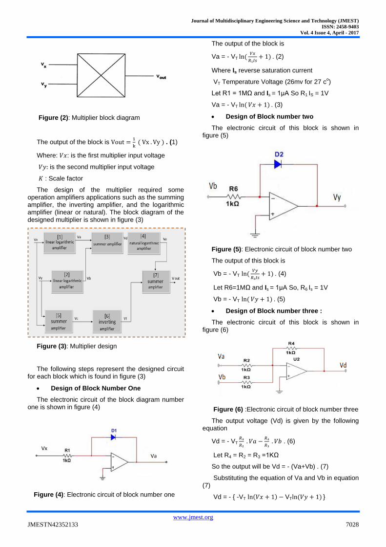
Design of Block number two
The electronic circuit of this block is shown in figure (5)
Figure (5): Electronic circuit of block number two
The output of this block is
Vb = - VT ln(𝑉𝑦
𝑅₆𝐼𝑠+ 1) . (4)
Let R6=1MΩ and Is = 1µA So, R6 Is = 1V
Vb = - VT ln( 𝑉𝑦 + 1) . (5)
Design of Block number three :
The electronic circuit of this block is shown in figure (6)
Figure (6) :Electronic circuit of block number three
The output voltage (Vd) is given by the following equation
Vd = - VT 𝑅₄
𝑅₂ . 𝑉𝑎 −
𝑅₄
𝑅₃ . 𝑉𝑏 . (6)
Let R4 = R2 = R3 =1KΩ
So the output will be Vd = - (Va+Vb) . (7)
Substituting the equation of Va and Vb in equation (7)
Journal of Multidisciplinary Engineering Science and Technology (JMEST) ISSN: 2458-9403
Vol. 4 Issue 4, April - 2017
www.jmest.org
JMESTN42352133 7030
order to check the performance of the multiplier circuit, first is the DC test and second AC test
Figure (11): Multiplier circuit
It’s important to make a test to ensure the results so there are two tests one of them is adding a DC input voltage and the output results was shown in table(1).
Table (1): DC test of Multiplier
Another test had been done when the two inputs are sinusoidal with different frequencies, the output, shown in figure (12)
Figure (12) AC test
B. Design of RF oscillator Block
The general block diagram of oscillator is given by the following figure (13)
Figure (13): General block diagram of oscillator
Where A is the gain of amplifier and B is the feedback factor of feedback network .The feedback factor is defined by
β = 𝑉𝑓
𝑉𝑜 .(18)
There are some of RF oscillators; one of them is colpitts circuit by using operational amplifier. The
colpitts oscillate is shown in figure (14)
Figure (14): Colpitts oscillator circuit
β = Vf
Vo from the above circuit Vf = −I ZC₂ Vo = I Z∁₁
Substituting the values of Vf and Vo in equation (18)
β = −I ZC₂
I ZC₁ =
1
j WC₂1
jWC₁
= −C₁
C₂ =
C₁
C₂ ∟180
o .(19)
The oscillator frequency of this circuit can be found by the following equation
f = 1
2π√LCeq . (20)
Where L is the inductor value Ceq is the equivalent
Journal of Multidisciplinary Engineering Science and Technology (JMEST) ISSN: 2458-9403
Vol. 4 Issue 4, April - 2017
www.jmest.org
JMESTN42352133 7032
Figure (18): Wein bridge oscillator circuit
After testing, the output waveform of the Wein bridge oscillator is given by the figure (19).
Figure (19): Wein bridge oscillator output wave form
The total sending of AM block and simulation can be shown in figure (20) which represents the total AM block system
Figure (20): The Total design of AM system block
The testing of the above circuit will be applied in order to find the modulation index for different values of amplitudes.
Modulation index
The AM modulation index is the measure of the amplitude variation surrounding an unmodulated carrier as with other modulation indices , in AM this quantity (also called modulation depth ) indicates how much the modulation varies around its orginal level .For AM it relates to variations in carrier amplitude and is defined as
Journal of Multidisciplinary Engineering Science and Technology (JMEST) ISSN: 2458-9403
Vol. 4 Issue 4, April - 2017
www.jmest.org
JMESTN42352133 7033
Table (3): Practical test of design
The samples of the output waveforms with respect the modulation index is shown in figures (21) ,(22) and (23)
Figure (21): The output waveform at modulation index (µ) = 0.4915
Fgure (22): The output waveform at modulation index (µ) = 0.9956
Figure (23): The output waveform at modulation index (µ) =1.4725
Conclusion:
AM is a kind of analog modulation and it is composed of several parts the most important parts are (modulator unit), (RF unit) and (audio unit) .In this project all these three parts were designed by using (operational amplifier) and and simulated by the program (Multisim version 12).The essential designed parts were examined to know the output waveform for every part to ensure that the design is compatible with the required conditions. After that the three parts were built in one system which represents the final design of AM system. The AM system was tested by entering signals which represents carrier signal and message signal with different amplitudes and at frequencies taken from the design of audio circuit and RF circuit, we noticed that the the output waveform was identical with the standards and after that the modulating index was calculated as a multiple case at multiple cases.
References:
1. MD. Ruhul Amin, Study of Amplitude Modulation (AM) and calculation of modulation index and SNR using Matlab. Paper published at 26 MAY 2010.
2. D.K.Sharma , A. Mishra& Rajiv Saxena, ANALOG & DIGITAL MODULATIONTECHNIQUES, Ujjain Engineering College, Ujjain, MP Madhav Institute of Technology & Science, Gwalior, MP,Jaypee Institute of Engineering & Technology, Guna, Mp 2008.
Study on the amplitude modulation of wind turbine noise: September 2013
4. W Les Huson, Huson & Associates Pty .AMPLITUDE MODULATION CASE STUDY AT THE LEONARDS HILL WIND FARM, VICTORIA, AUSTRALIA , AM Conference Cardiff 20 March 2014.
5. Nhut Minh Ngo, Masashi Unoki, and Ryota Miyauchi, Data Hiding Scheme for Amplitude Modulation Radio Broadcasting Systems, Japan Advanced Institute of Science and Technology 1-1 Asahidai, Nomi, Ishikawa,2013.
6. A. L. Chakraborty, W. Johnstone, M. Lengden, G. Stewart, K. Duffin ,Journal: Sensors and Actuators B-chemical - SENSOR ACTUATOR B-CHEM , vol. 150, no. 1, pp. 367-375, 2010