University of Tennessee, Knoxville University of Tennessee, Knoxville TRACE: Tennessee Research and Creative TRACE: Tennessee Research and Creative Exchange Exchange Masters Theses Graduate School 5-2019 Design and Switching Performance Evaluation of a 10 kV SiC Design and Switching Performance Evaluation of a 10 kV SiC MOSFET Based Phase Leg for Medium Voltage Applications MOSFET Based Phase Leg for Medium Voltage Applications Xingxuan Huang University of Tennessee, [email protected]Follow this and additional works at: https://trace.tennessee.edu/utk_gradthes Recommended Citation Recommended Citation Huang, Xingxuan, "Design and Switching Performance Evaluation of a 10 kV SiC MOSFET Based Phase Leg for Medium Voltage Applications. " Master's Thesis, University of Tennessee, 2019. https://trace.tennessee.edu/utk_gradthes/5464 This Thesis is brought to you for free and open access by the Graduate School at TRACE: Tennessee Research and Creative Exchange. It has been accepted for inclusion in Masters Theses by an authorized administrator of TRACE: Tennessee Research and Creative Exchange. For more information, please contact [email protected].
Transcript
University of Tennessee, Knoxville University of Tennessee, Knoxville
TRACE: Tennessee Research and Creative TRACE: Tennessee Research and Creative
Exchange Exchange
Masters Theses Graduate School
5-2019
Design and Switching Performance Evaluation of a 10 kV SiC Design and Switching Performance Evaluation of a 10 kV SiC
MOSFET Based Phase Leg for Medium Voltage Applications MOSFET Based Phase Leg for Medium Voltage Applications
Follow this and additional works at: https://trace.tennessee.edu/utk_gradthes
Recommended Citation Recommended Citation Huang, Xingxuan, "Design and Switching Performance Evaluation of a 10 kV SiC MOSFET Based Phase Leg for Medium Voltage Applications. " Master's Thesis, University of Tennessee, 2019. https://trace.tennessee.edu/utk_gradthes/5464
This Thesis is brought to you for free and open access by the Graduate School at TRACE: Tennessee Research and Creative Exchange. It has been accepted for inclusion in Masters Theses by an authorized administrator of TRACE: Tennessee Research and Creative Exchange. For more information, please contact [email protected].
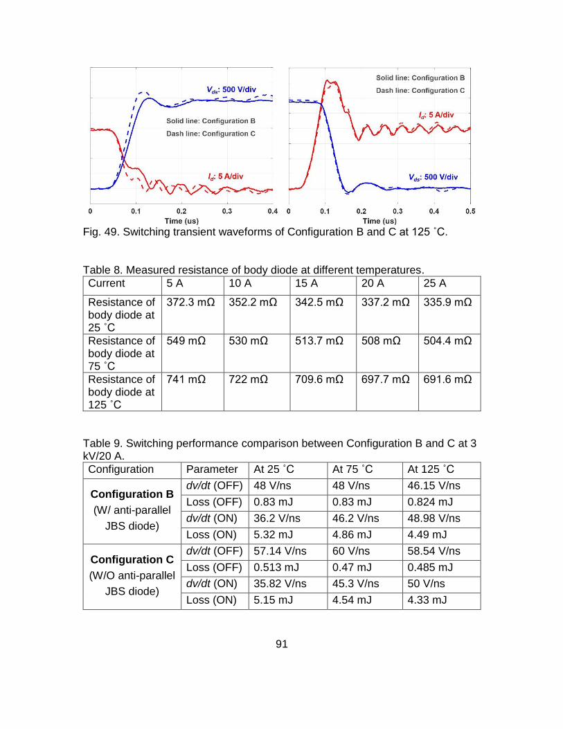
Fig. 49. Switching transient waveforms of Configuration B and C at 125 ˚C. ...... 91
Fig. 50. Nonlinear output capacitor of the anti-parallel SiC JBS diode. ............... 93
1
CH 1. INTRODUCTION
1.1 Medium Voltage Converters
Nowadays, more and more power flow is controlled and processed by
power electronics converters with high power conversion efficiency. Particularly,
medium voltage (MV, from 1 to 35 kV AC) power converters are playing a crucial
role in critical applications, including the modern grid and MV motor drives [1].
MV power converters have a wide range of applications in the power grid.
At the distribution level, various MV converters are needed to support the stable
operation of the grid, such as solid state circuit breaker and fault current limiter for
protection [2], [3], active power filter (APF) for improved power quality [4], static
synchronous compensator (STATCOM), and unified power flow controller. As the
capacity of the installed renewable energy sources keeps increasing, the efficient
interface for renewable energy sources draws increasing attention. MV converters
interface the renewable energy sources with the grid efficiently, with less stages
and less complicated structure. MV DC system is promising in interfacing the
utility-level solar farms to the grid with lower cost and higher efficiency, and
enables the possibility for DC transmission at the medium voltage level. New MV
converters have also been proposed to achieve smaller size and better
controllability, such as solid state transformer [6] and continuously variable series
reactor [7].
MV motor drives are indispensable driving forces in industrial,
transportation, and military applications. Motors and their drives consume a large
2
percentage of electricity supplied to industry. With the same power rating, MV
motor drives are able to achieve lower losses and higher power density compared
to low voltage drives [8]. MV variable speed drives are installed to drive
compressors in the oil and gas industry, high-power motors in mining and steel
industry, and so on. Trains and naval electric ships with higher DC-link voltage also
require MV drives [9].
Si-based power semiconductor devices dominate in current MV converters,
including IGBTs, thyristors, gate turn-off thyristors (GTOs), and integrated gate-
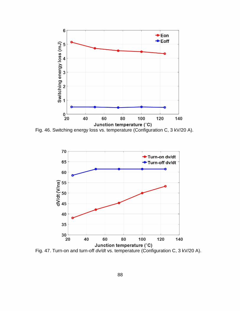
commutated thyristors (IGCTs). The Si IGBT shown in Fig. 1(a) is prevalent in MV
converters because of simple gate driver design and relatively high switching
frequency. Thyristors, GTOs, and IGCTs are only considered for extremely high
power applications, due to low conduction loss at large current. Si MOSFETs
shown in Fig. 1(b), with lower switching loss than Si IGBTs, typically cannot be
used in MV converters, otherwise the conduction loss is extremely large [10].
Fig. 1. Physical structure and current flow of IGBT and power MOSFET [10].
3
However, Si IGBTs have gradually become the bottleneck in the
development of high-performance MV converters. The limitations of Si IGBTs for
MV applications include relatively low blocking voltage, high switching loss, and
low switching frequency. Since the invention of IGBT in 1980s, the performance
improvement of Si IGBTs has driven the development of high-performance MV
converters. The design and fabrication process of Si IGBTs are mature and
approaching the limit of Si material. Power semiconductor devices with higher
blocking voltage are highly desirable, yet the voltage rating of Si IGBTs
commercially available for MV applications is limited to 6.5 kV, due to the
conduction losses. Also, because of current i2 in Fig. 1(a) that cannot be actively
shut down and the resulting tail current, it is difficult to further reduce the switching
loss of Si IGBTs [10]. The tail current during the turn-off transient contributes to a
large percentage of the switching loss. This is why the switching frequency of MV
converters based on 6.5 kV Si IGBTs is usually limited to 1 kHz. In summary, Si
IGBTs with limited blocking voltage and low switching frequency are not suitable
for future high-performance MV converters.
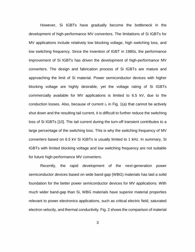
Recently, the rapid development of the next-generation power
semiconductor devices based on wide band-gap (WBG) materials has laid a solid
foundation for the better power semiconductor devices for MV applications. With
much wider band-gap than Si, WBG materials have superior material properties
relevant to power electronics applications, such as critical electric field, saturated
electron velocity, and thermal conductivity. Fig. 2 shows the comparison of material
4
Fig. 2. Summary of the material properties of Si, SiC, and GaN for power electronics applications [11]. properties of Si and two representative WBG materials, silicon carbide (SiC) and
gallium nitride (GaN). Particularly, SiC has the best maturity in wafer processing
and manufacturing as well as commercial availability of power semiconductor
devices among all promising WBG materials [11]. SiC has several different
polymorphic crystalline structures, each of which has different material properties.
In this thesis, only 4H-SiC is considered and discussed because it has the best
prospect in practical power electronics applications [12].
Excellent material properties of SiC bring the SiC power semiconductor
devices higher blocking voltage, higher operation temperature, and potential for
higher switching frequency. Since the release of the first commercially available
SiC Schottky barrier diode (SBD) in 2001, tremendous progress has been made
in SiC power semiconductor devices, including both low voltage and high voltage
5
devices, both majority carrier devices and minority carrier devices. A wide range
of high voltage SiC power semiconductor devices have been designed and
produced for MV applications, including junction barrier Schottky (JBS) diode,
MOSFET, IGBT, and thyristor [13]-[15]. Due to the ten times higher critical electric
field of SiC material, high voltage SiC devices are able to achieve much higher
voltage rating than their Si counterparts. With rated voltage ranging from 6.5 kV to
20 kV, these emerging SiC devices leveraging the superior characteristics of SiC
material are suitable for MV applications.
1.2 10 kV SiC MOSFETs for MV Applications
The 10 kV SiC MOSFET is one of the most promising high voltage SiC
power semiconductor devices to replace 6.5 kV Si IGBTs in MV applications [16]-
[19]. The on-resistance of the SiC MOSFET with blocking voltage up to 15 kV is
still acceptable, since SiC material tremendously reduces the drift layer resistance.
Research and development efforts have been spent on the 10 kV SiC MOSFET
for over a decade. As the leader in SiC power semiconductor devices,
Wolfspeed/Cree has designed and fabricated three generations of 10 kV SiC
MOSFETs, with the specific on-resistance reduced from 160 mΩ-cm2 to 100 mΩ-
cm2 at room temperature [16]-[19]. The latest 3rd generation 10 kV SiC MOSFET
is studied in this thesis. Compared to Si IGBTs for MV applications, 10 kV SiC
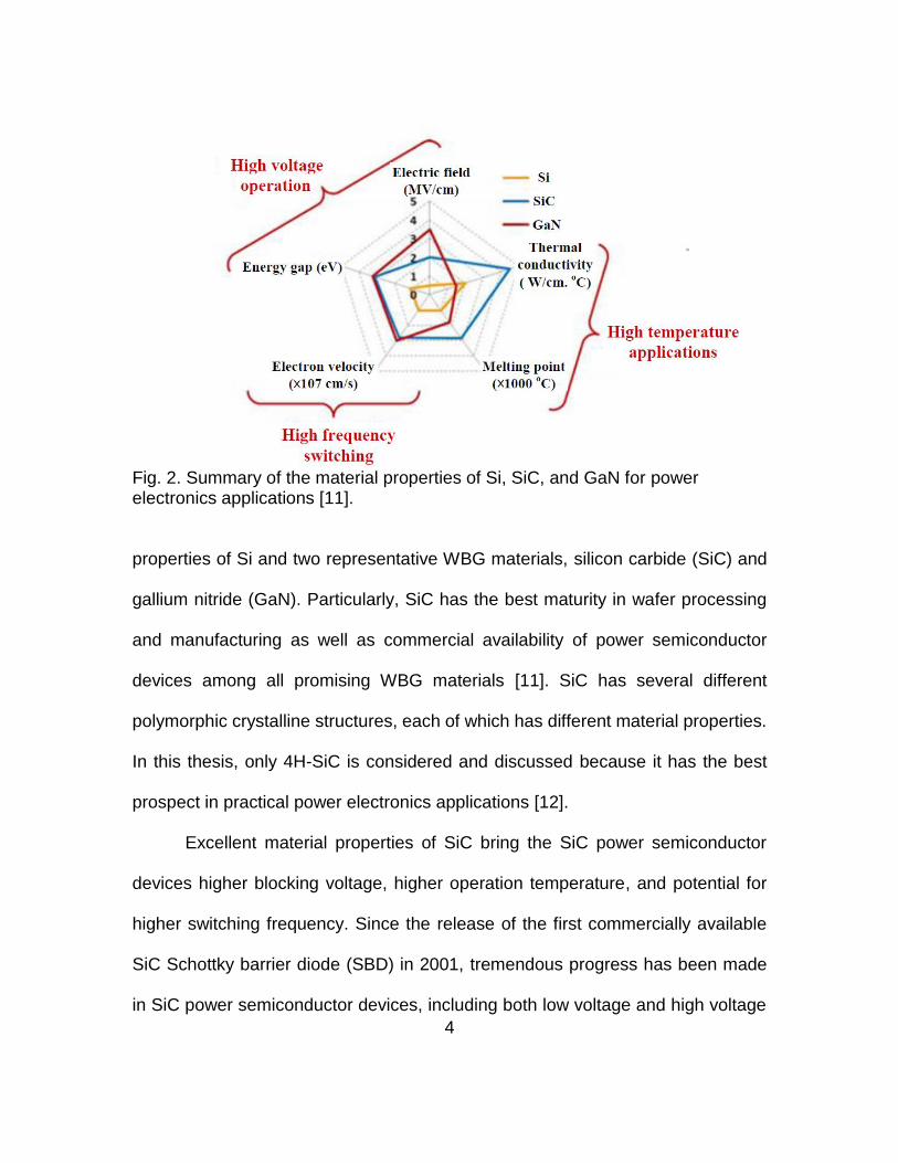
MOSFETs have higher voltage rating and operation temperature, lower switching
loss, and faster switching speed, as shown in Fig. 3. These benefits at the device
6
Fig. 3. Summary of device-level benefits and converter-level benefits of 10 kV. level further facilitate comprehensive benefits at the converter level, such as
simpler converter topology and design, higher efficiency, smaller size and weight,
and higher control bandwidth, which are also summarized in Fig. 3. Therefore, 10
kV SiC MOSFETs are promising to play a critical role in the future high-
performance MV converters.
10 kV SiC MOSFETs have relatively low on-resistance because of low
specific on-state resistance of SiC unipolar devices [20]. To achieve the same
blocking voltage level, much thinner drift layer and much higher doping density can
be used if Si wafer is replaced by SiC wafer. Therefore, the on-resistance of SiC
majority carrier devices is significantly reduced compared to their Si-based
counterparts at the same voltage level. Fig. 4 shows the comparison of the specific
on-resistance and its theoretical limit of SiC and Si majority carrier devices [20].
7
Fig. 4. Specific on-resistance vs. breakdown voltage for Si and SiC [20]. The newest generation of 10 kV SiC MOSFETs has specific on-resistance close
to its theoretical limit.
Furthermore, 10 kV SiC MOSFETs have faster switching speed, >20X lower
switching losses, and hence are able to switch at much higher frequency than 6.5
kV Si IGBTs with similar current rating [14], [19]. Due to the lower specific on-
resistance shown in Fig. 4, SiC MOSFETs typically have small die size, including
10 kV SiC MOSFETs. As a result, the parasitic capacitors are smaller, contributing
to the faster switching speed. The high saturated electron velocity of SiC material
also benefits the fast switching speed of 10 kV SiC MOSFETs. In the fundamental
point of view, the 10 kV SiC MOSFET as a majority carrier device, has faster
switching transients by eliminating the injection of minority charges and hence the
turn-off tail current, which is also illustrated in Fig. 1 [10]. The body diode of 10 kV
SiC MOSFETs also has much lower reverse recovery loss than Si PiN diodes,
8
which is attributed to the shorter minority carrier lifetime of SiC material [12].
MV converters benefit comprehensively from the superior performance of
10 kV SiC MOSFETs [17], [21]. The fast switching speed and low switching energy
loss give rise to the low converter switching loss. The volume and weight of the
cooling system could also be smaller. The switching frequency can be increased
to tens of kilohertz to achieve smaller size of passive components and higher
power density. The higher blocking voltage of 10 kV SiC MOSFETs reduces the
number of required devices and simplify the converter topology and design. With
10 kV SiC MOSFETs, two-level topologies can be adopted for MV drives with 4.16
kV line-to-line voltage. In MV motor drives, high switching frequency enabled by
10 kV SiC MOSFETs can support the high speed direct motor drives without the
gearbox, leading to smaller footprint and higher system density [22], [23]. Simpler
multi-level topologies can be used to directly interface the distribution grid by using
10 kV SiC MOSFETs, without the series connection of switching devices. These
benefits are also of great significance in emerging MV applications, such as electric
vehicle (EV) fast charger and data center power supply [21], [24].
In addition to benefits, fast switching speed of 10 kV SiC MOSFETs brings
new challenges. Generally these new challenges result from high dv/dt and high
di/dt generated by the fast switching speed. For instance, the drain-to-source
voltage Vds of the 10 kV SiC MOSFET typically falls from 6 kV to nearly 0 V within
100 ns during the turn-on transient. The high dv/dt (>60 V/ns) lasts for much longer
time than the dv/dt in low voltage (<6.5 kV) SiC MOSFETs. It is challenging to drive
9
the 10 kV SiC MOSFET while fully utilizing its fast switching speed. The gate driver
should isolate high voltage with high dv/dt in power and signal transmission. The
common-mode current and accelerated insulation degradation caused by high
dv/dt should be tackled, and the cross-talk issue should be evaluated and
addressed. Moreover, the fast switching speed makes the switching performance
of 10 kV SiC MOSFETs more sensitive to the parasitics in the power stage,
especially parasitic capacitors. It is still unknown what is these parasitic capacitors’
influence on the switching transients and performance of the 10 kV SiC MOSFETs.
1.3 Motivation and Objective
10 kV SiC MOSFETs are promising to boost the performance of MV
converters substantially, including the footprint, power density, specific power, and
efficiency. To apply the emerging advanced 10 kV SiC MOSFET in MV power
conversion systems, its switching behavior and performance should be
investigated and deeply understood. The investigation results are not only helpful
in understanding the switching transients of 10 kV SiC MOSFETs, but also
provides the switching energy loss data, design considerations, and guidelines for
the MV converters based on 10 kV SiC MOSFETs.
The half bridge phase leg is one of the most fundamental building blocks
for MV converters. It is the building block for two-level DC-DC bidirectional
converters, three-phase voltage source converters, and other MV converters. It
has two identical switching devices, and each switching device should have a
freewheeling diode to allow bi-directional current. The investigation results of half
10
bridge phase leg based on 10 kV SiC MOSFETs can be the foundation for the
study and design of more complicated building blocks and converters. The device’s
switching performance in the half bridge phase leg is widely accepted to guide the
converter loss estimation and design. Hence, this thesis concentrates on the study
of the half bridge phase leg based on 10 kV SiC MOSFETs. In this thesis, the
phase leg is defined as the half bridge phase leg with two identical switches
allowing bi-directional current.
In previous study, the switching performance of 10 kV SiC MOSFET has
been investigated with double pulse test (DPT), a commonly adopted method to
study the switching behavior and performance of a power semiconductor device.
With much faster switching speed than Si IGBTs, switching transients of 10 kV SiC
MOSFETs are more sensitive to the parasitics in the converter. Particularly,
parasitic capacitors in the power stage of the converter influence the switching
energy loss and dv/dt significantly and bring more ringing during the switching
transients. Nonetheless, the DPT setup for testing the 10 kV SiC MOSFETs is
often designed and built to minimize the parasitics in the power stage, and hence
have different characteristics from MV converters. In fact, the DPT setup usually
does not have the capability to operate continuously as part of a converter. As a
result, the conventional DPT setup is unable to identify and investigate the impact
of parasitic capacitors in the power stage on the switching performance. The
switching performance evaluation results with DPT sometimes deviate greatly from
11
what have been observed in converter operation, as reported in the study of low
voltage SiC MOSFETs [25], [26].
A phase leg with continuous operation capability as part of a MV converter
is an ideal platform to fully evaluate the switching performance of the 10 kV SiC
MOSFET and investigate the impact of the parasitic capacitors. One essential
issue in the phase leg design is how to design the robust gate driver for 10 kV SiC
MOSFETs when the phase leg is operating continuously [15]. It is also challenging
to test the phase leg and prove its continuous operation capability at dc-link voltage
higher than 6 kV. The testing should be nondestructive and extremely cautious,
because the 10 kV SiC MOSFET is expensive to produce and not commercially
available. Protection under overcurrent/short circuit conditions is necessary in the
gate driver to clear the fault before the MOSFET is damaged. In addition to the
overcurrent protection, more design considerations should be recognized in the
gate driver design to support the continuous operation.
The freewheeling diode also impacts the switching performance of the 10
kV SiC MOSFET in the phase leg, which can be implemented with body diode and
the external anti-parallel JBS diode. Typically, the body diode of SiC MOSFET has
small reverse recovery charge. Nonetheless, the reverse recovery performance of
the body diode of low voltage SiC MOSFETs becomes much worse as junction
temperature rises to 125 ˚C. Anti-parallel Schottky diode is recommended in
converters based on low voltage SiC MOSFETs to reduce reverse recovery current
and switching loss over a wide temperature range [11]. Regarding the 10 kV SiC
12
MOSFET, the impact of body diode and external anti-parallel JBS diode on the
switching behavior and loss has not been explored in detail to determine whether
to use anti-parallel diode in the converter.
The first motivation of this work is to design and test a 6.5 kV phase leg
based on 10 kV SiC MOSFET with continuous operation capability to serve as a
building block of a MV converter. The considerations and challenges of the design
and testing are explored. Then, the second motivation is to utilize the phase leg
prototype to evaluate the influence of the parasitic capacitors in the converter
power stage on the switching performance of 10 kV SiC MOSFETs with much
higher dv/dt than Si IGBTs. The third motivation is to conduct the quantitative
analysis about the impact of the freewheeling diode on the switching performance
of 10 kV SiC MOSFETs in order to clearly demonstrate the difference that adding
the anti-parallel JBS diode makes compared to using the body diode as the
freewheeling diode.
This thesis presents the detailed design and testing procedures of a 6.5 kV
phase leg based on the discrete 10 kV/20 A SiC MOSFETs from Wolfspeed with
continuous operation capability as a building block of a MV converter, with the
design of a robust gate driver for continuous operation introduced in detail. The
designed phase leg is utilized to evaluate the switching performance of the 10 kV
SiC MOSFET. The impact of the parasitic capacitors due to the load inductor and
the heatsink of the converter on the switching performance is investigated
comprehensively. To have a more complete understanding of the switching
13
performance of the 10 kV SiC MOSFET, the impact of the body diode and the anti-
parallel JBS diode on the switching performance is also studied in depth.
Meanwhile, the design principles are summarized to guide the MV converter
design based on 10 kV SiC MOSFETs.
1.4 Thesis Outline
The goal of this thesis is to evaluate the switching performance of the 3rd
generation 10 kV/20 A SiC MOSFET from Wolfspeed comprehensively, with the
impact of parasitic capacitors in the power stage of a MV converter considered. To
conduct the switching performance evaluation, a 6.5 kV half bridge phase leg is
designed and built for continuous operation as a building block of a MV converter.
The phase leg is fully tested and validated at 6.5 kV with the developed systematic
testing procedures.
Chapter 2 reviews the previous investigation of the switching performance
of 10 kV SiC MOSFETs with DPT. The design and testing of the 10 kV SiC
MOSFET based phase leg are also reviewed, focusing on the gate driver design
and overcurrent protection scheme. To have a more comprehensive review, the
progress in other high voltage SiC MOSFETs and IGBTs are also introduced.
Chapter 3 introduces the design and testing of the 6.5 kV half bridge phase
leg based on the discrete 10 kV/20 A SiC MOSFETs. The phase leg is designed
and tested to be capable of operating continuously at 6.5 kV dc-link voltage with
dv/dt up to 80 V/ns. Design considerations and challenges are presented in detail,
as well as the developed systematic testing procedures and testing results.
14
Chapter 4 investigates the impact of the parasitic capacitors in the converter
on the switching performance of the 10 kV SiC MOSFET with the DPT setup based
on the phase leg introduced in Chapter 3. The influence of the parasitic capacitors
caused by the load inductor and the heatsink on switching transients and losses is
investigated in detail.
Chapter 5 discusses the impact of the freewheeling diode on the switching
performance of 10 kV SiC MOSFETs. Specifically, the influence of body diode and
the added anti-parallel SiC JBS diode on the switching transients and losses is
studied in depth. The reverse recovery performance of the body diode is analyzed
over a wide temperature range. The switching performance with and without the
anti-parallel JBS diode is compared quantitatively to study the impact of adding
anti-parallel JBS diode.
Chapter 6 concludes the work presented in this thesis, and the future work
about the phase leg design and the switching performance investigation is
presented.
15
CH 2. LITERATURE REVIEW
Numerous efforts have been spent on the switching performance evaluation
of 10 kV SiC MOSFETs and the design of 10 kV SiC MOSFET based phase leg
recently, in order to apply this next-generation MOSFET in high-performance MV
power conversion systems in the future. The freewheeling diode in the phase leg
also attracts research interest, which can be the body diode or the added anti-
parallel JBS diode. In this chapter, the previous research efforts about the 10 kV
SiC MOSFETs will be summarized, including the switching performance
evaluation, phase leg design and test, and the selection of freewheeling diode.
Since the literature studying 10 kV SiC MOSFETs is still limited, the research about
other high voltage SiC devices (>6.5 kV) will also be reviewed.
2.1 Switching Performance Evaluation of 10 kV SiC MOSFETs
With fast switching speed, the switching performance of 10 kV SiC
MOSFETs is sensitive to numerous impact factors. Switching performance
evaluation should be conducted in detail to understand how to control the switching
transients and improve the switching performance. Typically, the switching
performance essential to the converter design is the research focus, especially the
switching energy loss and dv/dt. Switching loss contributes to a large portion of the
total converter loss in converters based on SiC devices with high switching
frequency, and it has profound influence on the switching frequency selection and
passive component design. The common mode noise caused by dv/dt poses great
challenge to the gate driver design with the isolated power supply and the control
16
circuits and signals [15], [27]. In addition, insulation issues occur if the high
blocking voltage also has high dv/dt [28].
The most common method to characterize the switching performance of a
power semiconductor device is DPT with the clamped inductive load circuit [11],
[29]. The basic operation principle of DPT is that the gate-to-source voltage Vgs of
the device under test (DUT) has two short pulses for the characterization of both
turn-on and turn-off transient in hard switching condition. Detailed working
principles of DPT will not be covered in this thesis. The essential aspects of DPT
include the control signal for DUT, the load inductor, the freewheeling path, and
the measurement setup. Two circuit configurations are usually used in DPT for the
switching performance characterization, depending on the complementary switch
to conduct the current when DUT is off. As shown in Fig. 5, the switch/switch pair
adopts the upper device which is always off to provide the current path when DUT
is off. The upper device and the DUT are identical. This configuration is also called
the phase leg configuration. In the switch/diode pair, a discrete diode with similar
current and voltage rating to the DUT is used as the freewheeling diode. The two
configurations are selected based on the purpose of DPT, and DPT configuration
should be similar to the intended converter [11]. The DUT is usually the lower
device because of its grounded source and the convenience in measurement. The
upper device can be the DUT as well, as displayed in Fig. 6. Then, the differential
voltage probe is required to measure the drain-to-source voltage of DUT. With a
hotplate or oven, the junction temperature of the DUT can be regulated.
17
(a) (b) Fig. 5. Two circuit configurations used in DPT: (a) switch/switch pair; (b) switch/diode pair.
(a) (b) Fig. 6. Two different kinds of DPT: (a) the lower device in the phase leg as the DUT; (b) the upper device in the phase leg as the DUT.
18
DPT has been commonly used to evaluate the switching performance of
high voltage SiC devices, including both the switch/diode pair and switch/switch
pair. The switching behavior and the impact of some factors have been revealed
by analyzing the switching waveforms and data. In [30], the DPT setup with
switch/diode pair is built to investigate the switching performance of the 15 kV SiC
MOSFET under different gate resistances and junction temperatures. It is found
that smaller gate resistance and higher junction temperature are able to accelerate
the turn-on process. The turn-off transient is mainly capacitive charging process
and hence is less dependent on gate driver parameters and the junction
temperature. The switching performance of 15 kV SiC IGBTs have also been
characterized with the switch/diode pair [30], [31], with both switching energy loss
and dv/dt analyzed in detail. Generally, DPT with switch/diode pair is helpful in
understanding the turn-on and turn-off transient and the influence of temperature
and gate driver, and it only requires one high voltage SiC device. However, it is
only suitable for evaluating the switching performance of the device in the
unidirectional DC-DC converter and other converters requiring either high-side or
low-side switch to be the diode, in terms of switching energy loss and dv/dt. DPT
configuration should be the same as the devices’ configuration in the converter to
have convincing evaluation of the switching performance. The data obtained in
DPT with switch/diode pair are not accurate to indicate the dv/dt and switching loss
of a two-level inverter or rectifier, whose fundamental building block is the phase
leg with two identical switches. In fact, the two-level inverter/rectifier, three-phase
19
or single phase, is prevalent in MV and high power applications. Therefore, DPT
with phase leg configuration in Fig. 5(a) is more preferable to evaluate the
switching performance of high voltage SiC devices for MV applications.
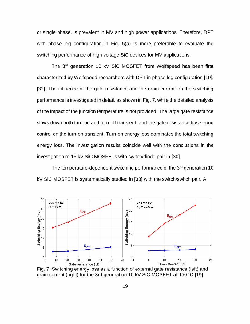
The 3rd generation 10 kV SiC MOSFET from Wolfspeed has been first
characterized by Wolfspeed researchers with DPT in phase leg configuration [19],
[32]. The influence of the gate resistance and the drain current on the switching
performance is investigated in detail, as shown in Fig. 7, while the detailed analysis
of the impact of the junction temperature is not provided. The large gate resistance
slows down both turn-on and turn-off transient, and the gate resistance has strong
control on the turn-on transient. Turn-on energy loss dominates the total switching
energy loss. The investigation results coincide well with the conclusions in the
investigation of 15 kV SiC MOSFETs with switch/diode pair in [30].
The temperature-dependent switching performance of the 3rd generation 10
kV SiC MOSFET is systematically studied in [33] with the switch/switch pair. A
Fig. 7. Switching energy loss as a function of external gate resistance (left) and drain current (right) for the 3rd generation 10 kV SiC MOSFET at 150 ˚C [19].
20
detailed device model in Fig. 8 is built to perform the systematic study of the
switching behavior and performance. Generally temperature has slight impact on
the turn-on transient and negligible effect on the turn-off transient, as indicated in
the switching waveforms in Fig. 9 and Fig. 10 (Rgoff = 3 Ω and Rgon = 15 Ω). During
the turn-off transient, the channel current drops to zero quickly due to low channel
current (<20 A) and high dv/dt. The turn-off process is thereby mainly the
charging/discharging of parasitic output capacitors of the MOSFETs, and dv/dt is
hence higher at higher load current. The parasitic capacitors are independent of
temperature. The junction temperature has little influence on the turn-off transient,
and the measured turn-off loss is mainly the energy stored in the output capacitor
of the DUT [33] [34].
Turn-on transient is slightly impacted by the temperature. The turn-on dv/dt
is higher at higher junction temperature due to the lower gate threshold voltage.
Meanwhile, the overshoot in drain current Id increases because of the increased
Fig. 8. Detailed device model of 10 kV SiC MOSFET [33].
21
Fig. 9. Turn-on (right) and turn-off (left) waveforms of the 10 kV SiC MOSFET at 25 ˚C [33].
Fig. 10. Turn-on (right) and turn-off (left) waveforms of the 10 kV SiC MOSFET at 125 ˚C [33].
22
displacement current in the parasitic capacitors. The turn-on loss reduces slightly
at higher temperature. Generally, junction temperature only slightly impacts the
switching transients of the 3rd generation 10 kV SiC MOSFET, and higher junction
temperature makes the turn-on transient faster. Such temperature-dependent
switching behaviors of 15 kV SiC MOSFETs have also been reported [35], [36].
In summary, DPT with both switch/switch pair and switch/diode pair has
been adopted to characterize the switching performance of 10 kV SiC MOSFETs
and other high voltage SiC devices. Characterization results show that the junction
temperature only has slight influence on the switching performance. The turn-on
transient of 10 kV SiC MOSFETs is mainly controlled by the gate driver
parameters, while the turn-off transient is mainly determined by the parasitic
capacitors since the channel current decreases to zero quickly.
Nevertheless, most previous studies have not investigated the impact of
parasitic capacitors in the MV converter on the switching performance of high
voltage SiC devices. The conventional DPT setup used in previous investigation is
designed to minimize the circuit parasitics, hence different from the real converters
with parasitics from numerous sources. For instance, the load inductor in
conventional DPT setup typically only has single-layer winding to reduce the
parasitic capacitor as much as possible, which is often not the case in MV
converters [31], [33]. In fact, the fast switching speed of SiC devices makes their
switching transients sensitive to the parasitic capacitors [37], [38]. If the parasitic
capacitors are negligible in DPT setup, the switching transients and losses
23
obtained in DPT could deviate significantly from experimental results in real
converters based on SiC devices. The switching loss in real converters could be
significantly higher than what is estimated based on DPT results [25], [26].
Therefore, it is necessary to investigate the impact of parasitic capacitors in the
converter on the switching performance of 10 kV SiC MOSFETs. To achieve this
target, the conventional DPT setup is not a suitable setup.
2.2 Design and Test of 10 kV SiC MOSFET Based Phase Leg
Half bridge phase leg is the fundamental building block for a variety of MV
converters. To have continuous operation capability, the phase leg usually consists
of two MOSFETs, the gate driver for MOSFETs, the busbar, and the heatsink. High
required voltage and high dv/dt bring numerous challenges in the design of the
phase leg, especially in the gate driver design and overcurrent protection design.
It is also challenging to determine how to test the phase leg comprehensively,
considering the high dc-link voltage and the expensive MOSFETs.
2.2.1 Gate Driver Design
The function of gate driver for the 10 kV SiC MOSFET is to drive the
MOSFET based on the PWM signal from the controller and protect the MOSFET
in short circuit/overcurrent conditions. The input of gate driver is the PWM signal
generated by the controller, and then in normal operation the gate driver follows
the input signal to output appropriate driving voltage and current for the turn-on
and turn-off of the device. When the short circuit or overcurrent happens, the gate
driver should be able to detect the fault and turn off the device safely to prevent
24
the device failure. For better clarity, the study of protection design will be reviewed
in the next subsection.
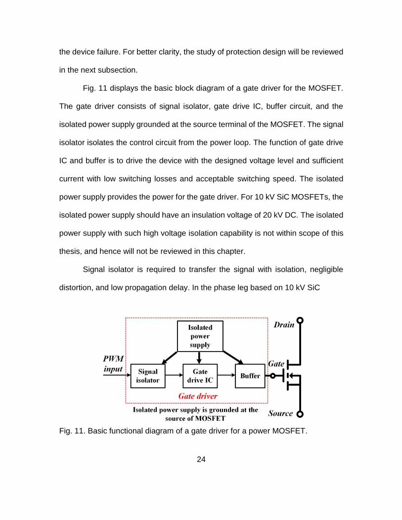
Fig. 11 displays the basic block diagram of a gate driver for the MOSFET.
The gate driver consists of signal isolator, gate drive IC, buffer circuit, and the
isolated power supply grounded at the source terminal of the MOSFET. The signal
isolator isolates the control circuit from the power loop. The function of gate drive
IC and buffer is to drive the device with the designed voltage level and sufficient
current with low switching losses and acceptable switching speed. The isolated
power supply provides the power for the gate driver. For 10 kV SiC MOSFETs, the
isolated power supply should have an insulation voltage of 20 kV DC. The isolated
power supply with such high voltage isolation capability is not within scope of this
thesis, and hence will not be reviewed in this chapter.
Signal isolator is required to transfer the signal with isolation, negligible
distortion, and low propagation delay. In the phase leg based on 10 kV SiC
Fig. 11. Basic functional diagram of a gate driver for a power MOSFET.
25
MOSFETs, the signal isolator in the gate driver for the upper MOSFET should
withstand the voltage bouncing periodically between 0 and dc-link voltage with high
dv/dt. The main challenge is to have high isolation voltage (>7 kV) and high
common mode transient immunity (CMTI) (>100 V/ns) simultaneously. The
propagation delay and maximum frequency range are not critical for the signal
isolator for 10 kV SiC MOSFETs with switching frequency typically lower than 80
kHz [21], [24].
Several kinds of off-the-shelf digital isolators are commercially available
with good CMTI and adopted in the gate drivers for low voltage SiC MOSFETs,
including capacitive solution, transformer-based solution, and opto-coupler.
However, none of them achieves the continuous isolation voltage of over 7 kV.
Furthermore, the clearance and creepage requirement should be satisfied in the
digital isolator. The clearance for 10 kV is 50 mm for the external traces in PCB
according to IPC-2221B standard [39].
Signal isolator solutions with over 7 kV isolation voltage for high voltage SiC
devices include the solutions based on planar transformer [40], coreless
transformer [41], and fiber optics. Among these solutions, the solution with fiber
optic transmitter and receiver has become the dominant solution. The isolation
voltage and CMTI of this solution can be extremely high if the power supplies in
each side offer sufficient isolation. With fiber optic cable, the clearance and
creepage requirements are easily satisfied. The typical propagation delay of the
transmitter and receiver is 30 ns. The total delay in signal isolation is less than 80
26
ns. The high signal rate (50 MBd) of the fiber optic transmitter and receiver ensures
the accurate transfer of PWM signals [42]. 5 V TTL logic is preferred with better
noise immunity, compared to 3.3 V TTL logic.
The gate drive IC and buffer operate together with gate resistors and other
auxiliary circuitry to drive the switching device and control the switching speed.
The buffer is optional and only adopted to increase the driving current. The gate
drive voltage and gate resistors are selected by considering the static
characteristics, switching performance, and short circuit performance. The off-
state gate voltage Vg,off for 10 kV SiC MOSFETs usually ranges from -6 V and -1
V. The negative Vg,off is implemented to ensure the reliable turn-off. For 10 kV SiC
MOSFETs, gate drive voltage in on state Vg,on ranges from 15 V to 20 V to have
low on-state resistance. Actually the on-resistance only has slight difference as
Vg,on increases from 15 V to 20 V [33], yet higher Vg,on increases the short circuit
current, leading to stricter requirement on the response time of the protection [43]
[44].
After Vg,on and Vg,off are selected, gate resistors are tuned to achieve the
desired switching transients and losses. Different gate resistors can be designed
for turn-on and turn-off transients. In the case of 10 kV SiC MOSFETs, gate
resistors are selected based on the trade-off between switching loss and switching
speed, especially during the turn-on transient. Then, the required peak driving
current can be calculated, in which the internal gate resistance should be
considered.
27
𝐼𝑠𝑜𝑢𝑟𝑐𝑒 =𝑉𝑔,𝑜𝑛−𝑉𝑔,𝑜𝑓𝑓
𝑅𝑔,𝑜𝑛 (𝑇𝑢𝑟𝑛 − 𝑜𝑛 𝑡𝑟𝑎𝑛𝑠𝑖𝑒𝑛𝑡) (1)
𝐼𝑠𝑖𝑛𝑘 =𝑉𝑔,𝑜𝑛−𝑉𝑔,𝑜𝑓𝑓
𝑅𝑔,𝑜𝑓𝑓 (𝑇𝑢𝑟𝑛 − 𝑜𝑓𝑓 𝑡𝑟𝑎𝑛𝑠𝑖𝑒𝑛𝑡) (2)
The selection of gate drive IC should particularly consider the peak driving
current, rise/fall time, and propagation delay. The peak source/sink drive current
of the gate drive IC should be higher than the required current, otherwise the buffer
is needed. The buffer can be IC with high driving current or BJT-based current
boosters in parallel [45], [46]. Short rise/fall time and propagation delay time are
required to fully utilize the fast switching speed of the 10 kV SiC MOSFETs.
The cross-talk issue should also be evaluated and tackled in the gate driver
design for high voltage SiC devices. In one half bridge phase leg, if dv/dt is too
high during the turn-on transient, the spurious gate voltage in the other device
could be higher than the gate threshold voltage with the current through the Miller
capacitor (gate-to-drain capacitor), resulting in partial shoot-through and higher
losses [47]. The cross-talk often sets the limit for the turn-on dv/dt of SiC
MOSFETs, if it is not addressed. The partial shoot-through has been reported in
the phase leg based on high voltage SiC MOSFETs when the turn-on gate
resistance is low [35].
Active Miller clamping is a common method to suppress the cross-talk
without sacrificing the switching speed [48], [49]. The gate driver for 10 kV/10 A
SiC MOSFET in [48] adopts an active Miller clamping design to maintain the off-
state of the MOSFET. When high dv/dt occurs during the turn-on transient of one
MOSFET, the gate driver for the other MOSFET in off state provides a low
28
impedance path for Miller capacitive current and clamps the gate voltage to ensure
the reliable turn-off. The clamping circuit is only activated when device is off.
Analytical analysis of cross-talk in low voltage SiC MOSFETs is also
effective in the evaluation of cross-talk of high voltage SiC devices. In fact,
previous analysis shows that cross-talk is not serious in some high voltage SiC
devices. After evaluating the cross-talk of 3rd generation 10 kV/20 A SiC MOSFET,
it is concluded that specific anti-cross-talk design is not necessary in the gate driver
[33]. The excellent performance in cross-talk is attributed to the much larger input
capacitance of the 10 kV/20 A SiC MOSFET, compared to its Miller capacitance.
The calculated maximum increase in Vgs is 5.0 V in the worst case when all Miller
capacitive current charges the input capacitor of MOSFET. Therefore, partial
shoot-through does not occur when Vg,off is below -4 V. DPT results of 10 kV SiC
MOSFETs show that the cross-talk has little impact on the turn-on transient and
loss (15 Ω turn-on gate resistor). Yet the spurious gate voltage is not measured
to provide the direct evidence.
In summary, the previous gate driver design for high voltage SiC devices
usually focuses on realizing fast switching speed and reliable isolation. Signal
isolation is typically achieved by fiber optics. The selection of components
emphasizes the driving capability and low delay. Cross-talk in the 3rd generation
10 kV SiC MOSFET is significantly alleviated by its large input capacitance, yet it
is an issue for some high voltage SiC devices with lower ratio between input
capacitor and Miller capacitor, such as 15 kV SiC MOSFETs from Wolfspeed [47].
29
With emphasis on the fast switching speed, most gate driver design for high
voltage SiC devices in the literature has not paid enough attention to the
continuous operation. During the continuous operation, the controller usually does
not know the status of the communication and the gate driver. The feedback signal
sent back to the controller only reports the overcurrent fault. Considering the higher
cost and less robustness of high voltage SiC devices, more efforts can be spent
on the continuous operation of the gate driver and the high voltage SiC device.
2.2.2 Overcurrent Protection Design
One critical function of the gate driver is the protection in overcurrent or
short circuit conditions. The protection is more crucial in MV and high power
applications, in which power semiconductor devices are more expensive. The
protection scheme should have fast response, good noise immunity, and easy
implementation. With smaller die and higher current density, SiC devices have
shorter short circuit withstand time than Si IGBTs and MOSFETs. Fast response
time is hence required, which inherently contradicts the strong noise immunity. The
fast switching transients of SiC devices makes it more challenging to achieve fast
response with sufficient noise immunity. Short response time is also desirable as
it benefits the long-term reliability. In this subsection, overcurrent protection
schemes for SiC MOSFETs are reviewed.
Desaturation (Desat) protection scheme commonly adopted for the
overcurrent protection of Si IGBTs has been successfully implemented in a variety
of SiC MOSFETs with fast response and strong noise immunity [49]-[51]. The
30
design shown in Fig. 12 for 1.2 kV SiC MOSFET has achieved a fast response
time of 210 ns [50]. Desat protection monitors the drain-to-source voltage drop Vds,
and the protection is triggered once the monitored Vds exceeds the threshold. The
desat diode with the same voltage rating as the MOSFET is necessary to isolate
the high voltage in the drain terminal. In desat protection, the blanking time is
needed to screen the voltage fall period during the turn-on transient and avoid the
false triggering, which accounts for a large percentage of the response time.
The threshold current of desat protection is determined by the device’s
output characteristic and the set threshold voltage. With the same drain current,
SiC MOSFETs have significantly higher Vds at higher junction temperature. Thus,
desat protection for SiC MOSFETs has different threshold currents as junction
temperature varies. The threshold current is higher at lower junction temperature.
Also, the drain current does not have hard saturation in SiC MOSFETs. In the
overcurrent or short circuit fault condition, the drain current continues rising
drastically during the delay time of desat protection, leading to the peak current
much higher than the threshold current. The current rise during the response time
should be taken into account when determining the threshold current.
Other overcurrent protection schemes for SiC MOSFETs have been
proposed by evaluating the current in a way independent of the output
characteristic of the MOSFET. The stray inductance in series with the source
terminal of the SiC MOSFET can be used as a sensor to derive the current and
serve for the protection, with the carried di/dt information [50], [51]. It is difficult to
31
Fig. 12. The implementation of desat protection for SiC MOSFETs [50]. implement this method for SiC MOSFETs with different packages and ensure high
noise immunity. A sufficient, but not too large, parasitic inductance with readily
connectible terminals is needed to implement this method. Then debugging in the
lab is necessary to measure the stray inductance for the threshold selection and
check the noise immunity. Protection schemes based on the current sensor are
also investigated. It is concluded that Rogowski coil has excellent overall
performance in terms of accuracy, bandwidth and linearity among numerous
current sensing methods, such as shunt resistor, Hall sensor, and current
transducer [52]-[54].
High-bandwidth Rogowski coil sensor with active integrator has been
demonstrated in the protection of SiC discrete devices and modules [53], [55]-[58].
PCB-based Rogowski coil stands out due to low profile, integration capability, and
repeatability. The protection scheme based on Rogowski coil detects the fault
32
within 100 ns, regardless of the short circuit type and the junction temperature. The
total response time is short and constant in different conditions, so the threshold
current can be easily selected. Nonetheless, the active integrator has to be reset
periodically when the device is off to overcome the difficulty of Rogowski coil in
measuring DC current, otherwise the sensor error keeps increasing [57], [58]. To
ensure the accuracy of the sensor and the protection, the device should be turned
off periodically with the off-state longer than a minimum length. The method is also
expensive and complicated, and requires more space for devices with large
package [55]-[58].
Among the reviewed overcurrent protection schemes, desat protection and
the protection based on PCB-based Rogowski coil are suitable for SiC MOSFETs,
with excellent overall performance, in terms of implementation, response time, and
noise immunity. Desat protection provides effective overcurrent protection for SiC
MOSFETs with low cost and easy implementation. The design process should
consider the variance of the threshold current in different conditions. Protection
based on Rogowski coil has constant threshold current in different conditions and
shorter response time, yet requires complicated implementation and high cost to
ensure sufficient sensor accuracy and noise immunity. The two methods should
be selected based on the specifications of the application.
2.2.3 Testing of the Phase Leg
The phase leg should be fully tested to validate its capability to operate
continuously at rated voltage and function as part of a MV converter. Continuous
33
test is hence required. The testing should be designed and implemented to make
sure that all components in the phase leg are fully validated at rated voltage.
Meanwhile, it is challenging to design the test procedures to endeavor to avoid the
damage of expensive high voltage SiC devices. Incremental testing steps should
be taken to qualify the components, especially the expensive SiC devices, before
the final continuous test.
How to test the phase leg or the converter based on high voltage SiC
devices comprehensively has received little discussion in previous literature. DPT
and short circuit test are usually conducted before the continuous test to validate
the SiC devices and the gate driver. MV converters based on high voltage SiC
devices have been designed and tested at rated voltage and power, yet the
detailed incremental testing steps are not covered. In [59], comprehensive testing
and qualification of the gate driver and its isolated power supply for high voltage
SiC MOSFETs and IGBTs are discussed in detail, including DPT, short circuit test,
and continuous test. The testing focuses on validating the gate driver’s thermal
performance and its performance in suppressing common mode current, including
the continuous test as the buck-boost converter with high common-mode voltage
magnitude. Nonetheless, the sequence of the testing is not clearly defined, and
only DC-DC continuous test is designed.
In summary, the testing of the phase leg based on high voltage SiC devices
has still not been fully discussed, although converters based on high voltage SiC
devices have been demonstrated at full power and voltage. The challenge is to
34
fully test the phase leg at rated voltage and meanwhile endeavor to minimize the
risk of damaging the expensive SiC devices during the test.
2.3 Freewheeling Diode for 10 kV SiC MOSFETs
It is required that every switch in the phase leg should provide the
freewheeling diode in voltage source converters and numerous DC-DC converters.
The freewheeling diode provides the conduction path for the load current when
both switches are off in the phase leg. In hard switching condition, the impact of
the freewheeling diode on the switching performance of Si devices and low voltage
SiC MOSFETs in the phase leg have been deeply understood. Considerations in
selecting the freewheeling diode are well explained. The reverse recovery of the
freewheeling diode with PN junction increases the current overshoot and energy
loss during the turn-on transient [10]. SiC MOSFETs have their own body diode
with small reverse recovery charge that can serve as the freewheeling diode [12].
Meanwhile, an external anti-parallel SiC Schottky diode with negligible external
reverse recovery charge can be added to function as the freewheeling diode during
the dead time.
Anti-parallel Schottky diode is recommended in converters based on low
voltage SiC MOSFETs to achieve stable switching energy loss at different junction
temperatures [11], [60]. This is because the body diode of the low voltage SiC
MOSFET has significantly worse reverse recovery performance as junction
temperature rises [60], [61]. The parasitic output capacitor of the Schottky diode
also causes increase in the switching loss. Hence, the SiC Schottky should be
35
selected to ensure that the reduction in switching loss due to improved reverse
recovery performance is more substantial than the increase in switching loss
brought by its parasitic capacitor [11], [60].
10 kV SiC JBS diode can be added as the anti-parallel diode to improve the
reverse recovery in the phase leg based on 10 kV SiC MOSFETs. Experimental
results have revealed that the anti-parallel 10 kV SiC JBS diode has nearly zero
reverse recovery charge at various temperatures [62]. Currently, the body diode of
10 kV SiC MOSFET is sufficiently reliable to function as the freewheeling diode
[63], [64]. In fact, several years ago, most 10 kV SiC MOSFETs available for
switching performance evaluation have an anti-parallel JBS diode inside the
package, because the MOSFET will degrade if body diode conducts current [65].
With the anti-parallel JBS diode inside the package, the JBS diode conducts a
major portion of the freewheeling current, and it is thereby difficult to study the
reverse recovery performance of the body diode and the impact of the body diode
or the external JBS diode on the switching transients and performance of 10 kV
SiC MOSFETs over a wide temperature range.
The reverse recovery performance of a diode is also commonly
characterized with DPT with a setup similar to the DPT setup for MOSFETs, as
drawn in Fig. 13. If the body diode of a MOSFET is under test, the channel of that
MOSFET is always kept off. With one terminal grounded, the diode under test is in
parallel with the load inductor. When the upper switch S turns on, the diode current
is forced to commutate to the upper switch, and the reverse recovery performance
36
can be evaluated by measuring the diode current. With DPT, researchers at
Wolfspeed have characterized the body diode of the 3rd generation 10 kV/20 A SiC
MOSFET, revealing that the body diode has the reverse recovery charge of 1.2 μC
and 1.8 μC at 25 ˚C and 150 ˚C, respectively [14]. The measured reverse recovery
current, however, also includes the displacement current in parasitic capacitor Cj
which is charged during the turn-on process of the upper switch. Because of the
high dv/dt of the upper switch, the 10 kV SiC MOSFET in this case, the capacitive
current accounts for a large portion of the measured reverse recovery current.
The substantial effect of the capacitive current on the reverse recovery
characterization of 10 kV SiC diodes is demonstrated in [66]. After eliminating the
effect of the capacitive current, the calculated reverse recovery current Irr of the
body diode in 10 kV/10 A SiC MOSFET is lower than 2 A at 25 ˚C and 125 ˚C. The
reverse recovery charge of the body diode is not calculated. It is concluded that
the body diode of the 10 kV SiC MOSFET has small reverse recovery current at
different temperatures.
Fig. 13. Circuit diagram of DPT for diode reverse recovery characterization.
37
In summary, the freewheeling diode in the phase leg plays an essential role
in the switching transients of 10 kV SiC MOSFETs, especially the turn-on transient.
The reverse recovery characterization of the freewheeling diode for 10 kV SiC
MOSFETs should consider the effect of the capacitive current due to the parasitic
capacitor of the diode. The reverse recovery current of the body diode in 10 kV/10
A SiC MOSFET is lower than 2 A at 25 ˚C and 125 ˚C, but the reverse recovery
charge is not calculated. What is the impact of the reverse recovery of body diode
on the switching performance is still unknown at different temperatures. Neither is
the outcome after adding the anti-parallel JBS diode with nearly zero reverse
recovery charge.
2.4 Summary
Previous work on the switching performance evaluation of 10 kV SiC
MOSFETs and other high voltage SiC devices and the design of the phase leg
based on high voltage SiC devices is reviewed in this chapter. First, the switching
performance evaluation with DPT is reviewed together with the impact factors of
the switching performance. Then, the existing work on the design and validation of
the phase leg based on the high voltage SiC devices is presented, especially the
gate driver design with overcurrent protection and the testing of the phase leg. In
the end, freewheeling diode candidates for the phase leg based on 10 kV SiC
MOSFETs and the study of their reverse recovery performance are reviewed,
including the body diode and the anti-parallel SiC JBS diode.
38
CH 3. DESIGN AND TEST OF A 10 KV SIC MOSFET BASED
PHASE LEG
The design of a half bridge phase leg based on 10 kV SiC MOSFETs with
continuous operation capability is introduced in this chapter, which is validated in
the continuous test at 6.5 kV dc-link voltage with dv/dt up to 80 V/ns. The design
target of the phase leg is the continuous operation as one building block of a MV
power conversion system. To achieve the target, the design considerations and
details of the high-speed gate driver and overcurrent protection for the 10 kV SiC
MOSFET are discussed, and the testing procedures and results of the phase leg
are presented in detail.
3.1 Overview of the Phase Leg
3.1.1 10 kV SiC MOSFET
The half bridge phase leg is based on 10 kV/20 A discrete SiC MOSFETs
from Wolfspeed (XPM3-10000-0350B). The device has a non-isolated package
with the large drain plate also for heat dissipation, as shown in Fig. 14. Gate
terminal and source terminal are on the top of the package. Inside the package is
one 3rd generation 10 kV/350 mΩ SiC MOSFET die. The die only has one wire
bond for the connection with the gate terminal, forming a weak connection point in
the package.
Characterization results with a curve tracer show that the 10 kV SiC
MOSFETs available for the phase leg construction have almost the same on-
resistance in forward conduction and reverse conduction with the same gate
39
voltage and junction temperature. The 3rd generation 10 kV/350 mΩ SiC MOSFET
does not have the degradation issue during the body diode conduction [63], [64].
Therefore, the body diode is used as the freewheeling diode, and external anti-
parallel JBS diode is not needed in the phase leg. The body diode conducts
reverse current and serves as the freewheeling diode during the dead time. Gate-
to-source voltage Vgs has little influence on the on-resistance as long as it exceeds
15 V, as indicated in Fig. 14. As the junction temperature increases from 25 ˚C to
150 ˚C, the on-resistance keeps increasing to over 0.8 Ω.
3.1.2 Architecture of the Phase Leg
The designed 6.5 kV half bridge phase leg consists of two MOSFETs, two
isolated power supplies, the gate driver, the heatsink, the PCB busbar, and the dc-
link capacitor. The architecture of the phase leg is shown in Fig. 15(a). Such
architecture is designed to ensure that the phase leg has the capability to operate
as a building block for a modular MV converter. The communication interface
Fig. 14. Discrete 10 kV SiC MOSFET in the half bridge phase leg (left) and its forward characteristic at room temperature (right).
40
marked in green in Fig. 15(a) communicates with the controller via fiber optics with
reliable signal isolation. Four terminals are available for connection, including DC+,
DC-, midpoint of DC-link, and midpoint of the half bridge phase leg. The phase leg
has an 8.75 μF dc-link capacitor, realized by placing four 1.9 kV/35 µF film
capacitors in series. The rated dc-link voltage of the phase leg is 6.5 kV, with 1.1
kV margin for overvoltage during the switching transients.
The detailed three-dimensional (3D) design of the phase leg is drawn in Fig.
15(b). A gate driver board is placed above the two MOSFETs to drive the devices,
powered by two isolated power supplies. Part of the power loop is realized in the
gate driver board. To connect the drain plate in the bottom of the device package,
high voltage wires are utilized. The PCB busbar finally finishes the power loop by
connecting the dc-link capacitor with the MOSFETs. FR4 is the insulation material
in the PCB busbar, and better material can be adopted for more reliable insulation.
(a) (b) Fig. 15. Half bridge phase leg based on 10 kV SiC MOSFETs: (a) Architecture of the phase leg; (b) Detailed 3D model of the phase leg.
41
Each MOSFET in the phase leg has a separate floating heatsink for heat
dissipation. The heatsink is not isolated from the MOSFET, hence the heatsink has
the same potential as the drain plate of the MOSFET it is connected to. During the
continuous operation, a fan is used to cool devices and heatsinks.
3.2 Gate Driver Design
The gate driver for the 10 kV/20 A SiC MOSFETs is designed to realize fast
switching speed and robust continuous operation of the MOSFET. To achieve the
target, especially in continuous operation condition, specifications of the gate
driver are developed and summarized in Table 1. The main challenges are high
voltage insulation and high dv/dt. The gate driver board is designed to meet the
clearance and creepage requirement for 10 kV to achieve robust insulation [39].
The dead time function in the gate driver is desirable to prevent the shoot-through,
regardless of the input gate signal. Feedback signal sent back to the controller in
every switching cycle, as shown in Fig. 15, is necessary for the controller to monitor
the status of the communication and gate driver during the continuous operation.
If a short circuit or overcurrent fault is detected, a fault signal is sent back to the
controller via a feedback signal.
The specifications in Table 1 have been successfully achieved in the
designed gate driver, which is composed of signal transfer and feedback stage,
gate driving stage, and overcurrent protection stage. The block diagram of the gate
driver is shown in Fig. 16, in which three stages in the gate driver are marked with
different colors.
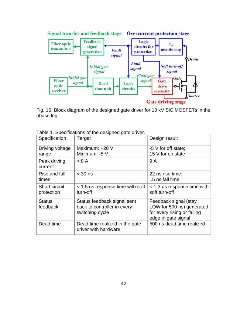
42
Fig. 16. Block diagram of the designed gate driver for 10 kV SiC MOSFETs in the phase leg. Table 1. Specifications of the designed gate driver.
Specification Target Design result
Driving voltage range
Maximum: +20 V Minimum: -5 V
-5 V for off state; 15 V for on state
Peak driving current
> 8 A 9 A
Rise and fall times
< 30 ns 22 ns rise time; 15 ns fall time
Short circuit protection
< 1.5 us response time with soft turn-off
< 1.3 us response time with soft turn-off
Status feedback
Status feedback signal sent back to controller in every switching cycle
Feedback signal (stay LOW for 500 ns) generated for every rising or falling edge in gate signal
Dead time Dead time realized in the gate driver with hardware
500 ns dead time realized
43
3.2.1 Signal Transfer and Feedback Stage
Signal transfer and feedback stage is responsible for the communication
between the controller and the gate driver during the continuous operation. The
communication is realized with fiber optics to provide ample signal isolation
between the controller and the gate driver with high voltage and high dv/dt. The
gate driver has one receiver for input PWM signal and one transmitter for feedback
signal sent back to controller, as can be seen in Fig. 16.
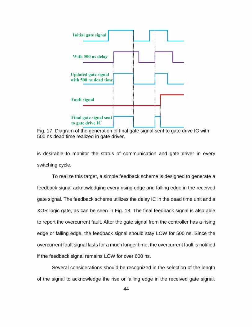
The dead time function is implemented with a delay IC in this stage. The
delay IC (DS1100Z-500+ from Maxim) generates the signal with 500 ns delay. With
a AND logic IC and the delay IC, the dead time is realized by applying 500 ns delay
to the rising edge of the initial gate signal and zero delay to the falling edge. The
updated gate signal becomes the final gate signal for gate drive IC if overcurrent
fault is not detected. The final gate signal is always LOW if the overcurrent
protection is triggered until it is reset. The generation of the gate signal sent to the
gate drive IC is summarized in Fig. 17.
The feedback signal sent from the gate driver is essential in the continuous
operation. In most gate drivers for SiC power devices reported in the literature, the
feedback signal is only designed to transmit the overcurrent fault signal. In this
case, the controller knows nothing about the status of the gate driver and
communication. For example, if the fiber optic receiver in the gate driver fails, the
controller will not know that it actually loses control of the state of the MOSFET.
The controller is not notified until the overcurrent happens. Such delay is not
acceptable in a MV converter. Hence, a feedback signal sent back to the controller
44
Fig. 17. Diagram of the generation of final gate signal sent to gate drive IC with 500 ns dead time realized in gate driver. is desirable to monitor the status of communication and gate driver in every
switching cycle.
To realize this target, a simple feedback scheme is designed to generate a
feedback signal acknowledging every rising edge and falling edge in the received
gate signal. The feedback scheme utilizes the delay IC in the dead time unit and a
XOR logic gate, as can be seen in Fig. 18. The final feedback signal is also able
to report the overcurrent fault. After the gate signal from the controller has a rising
edge or falling edge, the feedback signal should stay LOW for 500 ns. Since the
overcurrent fault signal lasts for a much longer time, the overcurrent fault is notified
if the feedback signal remains LOW for over 600 ns.
Several considerations should be recognized in the selection of the length
of the signal to acknowledge the rise or falling edge in the received gate signal.
45
This feedback scheme requires the conduction time of the 10 kV SiC MOSFET to
be longer than the signal for the acknowledgement. Long feedback signal for
acknowledgement limits the duty cycle when the MOSFET operates at higher
frequency. The discrete 10 kV SiC MOSFETs have the switching frequency up to
80 kHz in soft-switching converters [21], [24]. The long feedback signal for the
acknowledgement also leads to long delay time for the controller to identify the
overcurrent fault based on the received feedback signal. The feedback signal for
the edge acknowledgement should also not be too short for the controller to read.
In this case, it could be overwhelmed by the highly unpredictable noise in the
feedback signal. Finally, the feedback signal for the edge acknowledgement is
determined to be 500 ns LOW to have strong noise immunity, and it only requires
the duty cycle higher than 4% at 80 kHz switching frequency.
Fig. 18. Diagram of the generation of final feedback signal sent back to controller.
46
The designed feedback scheme can monitor the status of fiber optic
communication and numerous components in the gate driver. If any of the gate
driver components inside the green box in Fig. 19 fails, the feedback signal will not
be correct. The delay IC in the dead time unit is also monitored, since it is utilized
for feedback signal generation. If the feedback signal does not turn LOW within
200 ns after the rising or falling edge in the gate signal, the fault is detected by the
controller. Therefore, the designed feedback signal is helpful in monitoring the
status of the fiber optic communication and the gate driver and is able to quickly
detect the fault.
3.2.2 Gate Driving Stage
The core of the gate driving stage is the gate drive IC. Signal isolation is not
required in the gate drive IC since the fiber optics provide ample isolation for the
input PWM signal. The gate drive IC is selected based on the developed
specifications in Table 1. The main considerations are peak driving current, rise/fall
Fig. 19. Components in the gate driver which are monitored through the feedback signal sent back to the controller (inside the green box).
47
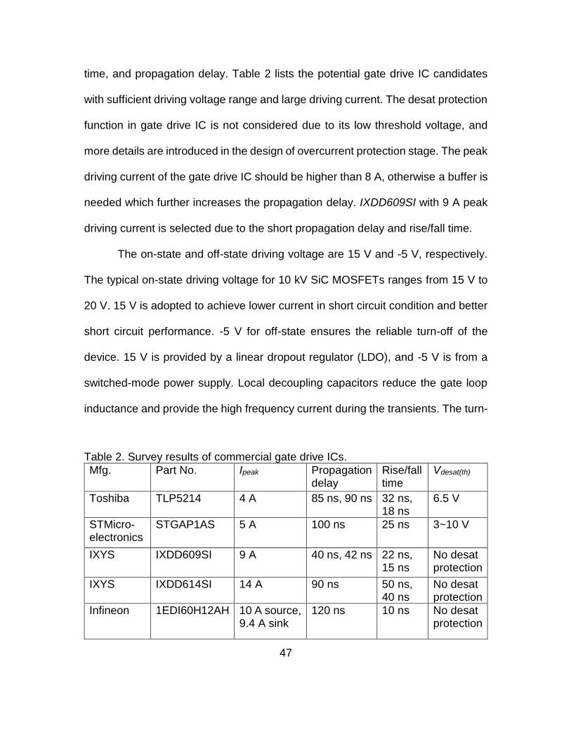
time, and propagation delay. Table 2 lists the potential gate drive IC candidates
with sufficient driving voltage range and large driving current. The desat protection
function in gate drive IC is not considered due to its low threshold voltage, and
more details are introduced in the design of overcurrent protection stage. The peak
driving current of the gate drive IC should be higher than 8 A, otherwise a buffer is
needed which further increases the propagation delay. IXDD609SI with 9 A peak
driving current is selected due to the short propagation delay and rise/fall time.
The on-state and off-state driving voltage are 15 V and -5 V, respectively.
The typical on-state driving voltage for 10 kV SiC MOSFETs ranges from 15 V to
20 V. 15 V is adopted to achieve lower current in short circuit condition and better
short circuit performance. -5 V for off-state ensures the reliable turn-off of the
device. 15 V is provided by a linear dropout regulator (LDO), and -5 V is from a
switched-mode power supply. Local decoupling capacitors reduce the gate loop
inductance and provide the high frequency current during the transients. The turn-
Table 2. Survey results of commercial gate drive ICs.
Mfg. Part No. Ipeak Propagation delay
Rise/fall time
Vdesat(th)
Toshiba TLP5214 4 A 85 ns, 90 ns 32 ns, 18 ns
6.5 V
STMicro-electronics
STGAP1AS 5 A 100 ns 25 ns 3~10 V
IXYS IXDD609SI 9 A 40 ns, 42 ns 22 ns, 15 ns
No desat protection
IXYS IXDD614SI 14 A 90 ns 50 ns, 40 ns
No desat protection
Infineon 1EDI60H12AH 10 A source, 9.4 A sink
120 ns 10 ns No desat protection
48
on and turn-off gate resistance are 15 Ω and 3 Ω, respectively, to achieve the
trade-off between switching speed and switching loss.
With -5 V Vgs in off state, active Miller clamp circuit to prevent cross-talk is
not necessary for the 3rd generation 10 kV/20 A SiC MOSFET, thanks to its large
ratio between input capacitance and Miller capacitance [33]. The 15 Ω turn-on
resistance and 3 Ω turn-off resistance are also helpful in limiting the turn-on dv/dt
to 80 V/ns and the spurious gate voltage [67]. Two transient voltage suppression
(TVS) diodes are added between the gate and the source to clamp Vgs at 16 V and
-5.4 V when there is abnormal oscillations in the gate.
3.2.3 Overcurrent Protection Stage
Among the several overcurrent protection schemes for SiC MOSFETs,
desat protection scheme stands out in the protection of the discrete 10 kV/20 A
SiC MOSFETs. Desat protection has relatively easy implementation to achieve
fast response time, high noise immunity, and effective protection in different cases.
Other methods, such as protection based on Rogowski coils, require much more
efforts in design and testing to guarantee high noise immunity.
The designed desat protection scheme protects the 10 kV SiC MOSFET in
short circuit/overcurrent condition with a response time of less than 1.3 μs. After
the fault is detected, soft turn-off is applied with a gate resistance of 47 Ω to safely
turn off the MOSFET, and the fault is reported to the controller via the feedback
signal. The short circuit withstand time of the 3rd generation 10 kV/20 A SiC
MOSFETs typically range from 2 μs to 10 μs. Such a wide range of short circuit
49
performance is reasonable since the device is still under in R&D stage and not
mature enough for commercial applications. Wolfspeed has also reported the 3rd
generation 10 kV SiC MOSFET with enhanced short circuit performance and over
13.6 μs short circuit withstand time at 5 kV [14]. Therefore, the protection should
respond within 1.5 μs after a short circuit or overcurrent fault occurs to safely
protect the MOSFET. Considering the tolerance of components and other non-
ideal factors, the specification for the response time is 1.3 μs.
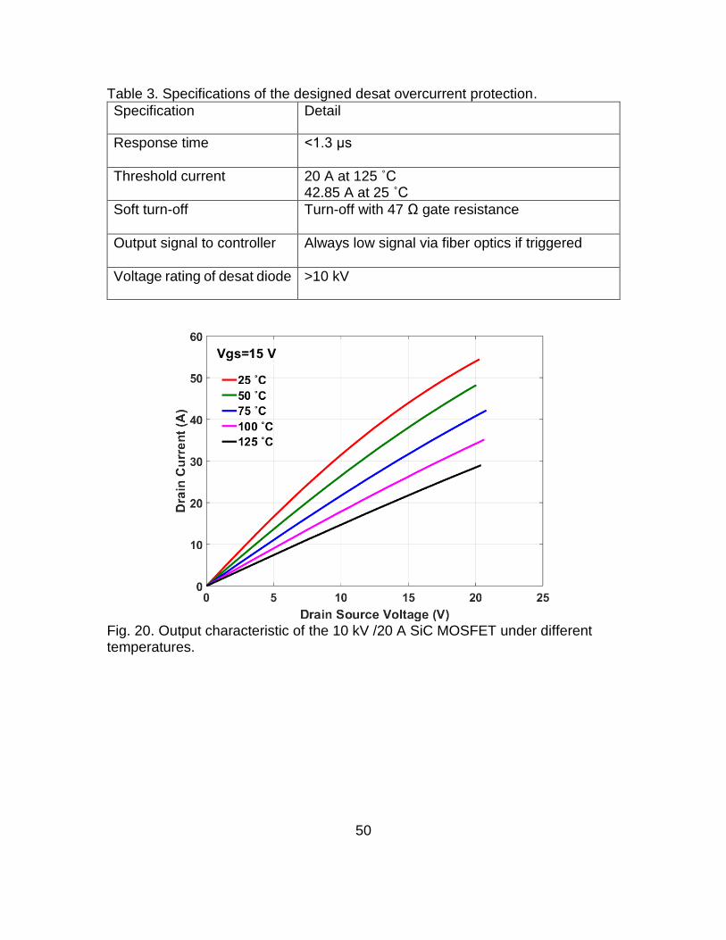
The threshold voltage of desat protection is determined based on the output
characteristic of the 10 kV/20 A SiC MOSFET, which is heavily influenced by the
junction temperature, as illustrated in Fig. 20. The threshold current is lower at
higher temperature due to the higher on-state voltage drop. The threshold voltage
is selected based on the output characteristic at 125 C to avoid the false triggering
during the normal operation at lower junction temperature. The threshold current
should be set as low as possible, since the drain current of the SiC MOSFET still
increases rapidly in active region. In other words, the drain current of the SiC
MOSFET stills rises significantly during the response time, and the drain current
cannot be clamped by the MOSFET, which further increases the short circuit
energy loss. At 125 ˚C, the selected threshold current is 20 A, the rated current of
the 10 kV SiC MOSFET. Taking into account slight variances in the output
characteristic among different devices, the threshold voltage is 15 V, leading to
42.85 A threshold current at 25 ˚C. The specifications of the designed desat
protection are summarized in Table 3.
50
Table 3. Specifications of the designed desat overcurrent protection.
Specification Detail
Response time <1.3 μs
Threshold current 20 A at 125 ˚C 42.85 A at 25 ˚C
Soft turn-off Turn-off with 47 Ω gate resistance
Output signal to controller Always low signal via fiber optics if triggered
Voltage rating of desat diode >10 kV
Fig. 20. Output characteristic of the 10 kV /20 A SiC MOSFET under different temperatures.
51
In addition, the voltage drop on the desat diode should be considered when
determining the threshold voltage. The desat diode blocks the dc-link voltage when
the MOSFET is in off state to protect the desat protection circuitry. The rated
voltage of the desat diode should be the same as that of the MOSFET to achieve
good reliability. The desat diode with 10 kV blocking voltage is implemented with
four 3.3 kV SiC Schottky diodes (GAP3SLT33-220FP) in series together with
balancing resistors. The pads in PCB for the 3.3 kV diode are coated with insulation
material (Konform SR). Such design ensures good commercial availability and
robustness. Also, the parasitic capacitance in parallel with the desat diode and the
displacement current are reduced effectively, which significantly benefits the noise
immunity of the protection. Still, the implementation with four diodes introduces 4
V total voltage drop [68]. Thus, the eventual selected threshold voltage is 19 V for
the desat protection.
Desat protection can be implemented by either the gate drive IC with desat
protection function or the circuitry based on discrete components. The gate drive
IC with desat protection usually requires large blanking capacitor to suppress the
noise in high dv/dt conditions, leading to long response time. Also, the 19 V
threshold voltage for the 10 kV/20 A SiC MOSFET is much higher than the
threshold of desat protection provided by the gate drive IC. With better flexibility to
achieve strong noise immunity, the circuitry based on discrete components is
hence designed to realize desat protection, and the details are shown in Fig. 21,
in which the parasitic capacitors marked in red should be considered in the design.
52
Fig. 21. Implementation of desat protection in the gate driver for 10 kV SiC MOSFETs. Resistors R1, R2, and blanking capacitor Cblk together realize the blanking time
which prevents the false triggering during the turn-on transient when the drain-to-
source voltage Vds drops quickly to on-state voltage. The clamping diode Dblk limits
the voltage Vdesat to 21 V to protect the comparator. The comparator and the logic
control circuit are grounded at -5 V. Resistor Rcla (20 Ω) and MOSFET Mcla clamps
Vdesat at -5 V when the 10 kV SiC MOSFET is shut off, and they prevent the false
triggering due to the high dv/dt during the turn-off transient.
The response time of desat protection is mainly determined by the blanking
time. The blanking time should not be over until the drain-to-source voltage Vds
drops to on-state voltage without ringing. If blanking time is too short, Vdesat will be
charged to exceed the threshold before it is clamped by Ddesat. It is necessary to
check the turn-on transients of the 10 kV SiC MOSFET to set a suitable blanking
time. Preliminary DPT results show that required blanking time is longer if the load
53
current is higher. According to the DPT results at 6.25 kV/20 A with the same gate
driver parameters (see Fig. 22), it takes 480 ns for Vds to reach steady state, after
Vgs starts to rise. The junction temperature has little influence on the length of this
time interval. Considering the delay in gate drive IC, the blanking time should be
longer than 550 ns to avoid the false triggering of the protection when the 10 kV
SiC MOSFET turns on normally. The minimum response time that can be achieved
by the designed desat protection is 600 ns with enough noise immunity.
High noise immunity during the turn-off transient with positive dv/dt is
necessary for desat protection. The displacement current through the parasitic
capacitor of the desat diode charges Cblk and increases Vdesat during the turn-off
transient with positive dv/dt, and the protection can be falsely triggered. The
oscillation owing to the high dv/dt makes the situation worse. To damp the ringing
Fig. 22. Turn-on transient of the 10 kV SiC MOSFET at 6.25 kV/20 A.
54
due to high dv/dt, a small resistor R2 (47 Ω) is added. Rcla and Mcla are designed
to clamp Vdesat before high turn-off dv/dt occurs. In other words, the clamp should
be effective within the turn-off delay time. If the gate signal has a falling edge, Vdesat
is pulled down to -5 V after 80 ns delay. Vdesat is solidly clamped at -5 V before the
positive dv/dt occurs during the turn-off transient. A RC circuit is added in the gate
of Mcla to realize the 80 ns delay and suppress the noise at the gate of Mcla. During
the turn-on transient, Vdesat is also clamped at -5 V for 80 ns before it starts to rise.
Hence, the 80 ns delay in the gate of Mcla is part of the blanking time.
The blanking time is tuned by changing R1 and Cblk. The blanking time is
indeed the time it takes to charge Vdesat from -5 V to the 19 V threshold voltage Vth.
Hence, all parasitic capacitors between Vdesat and -5 V should be considered,
including nonlinear parasitic capacitors from Dblk and Mcla as well as the capacitor
due to the PCB layout. The blanking time is calculated with the following equations.
𝑡𝑏𝑙𝑘 = 𝜏 𝑙𝑛 (𝑉𝑐𝑐+5
𝑉𝑐𝑐−𝑉𝑡ℎ) (3)
𝜏 = 𝐶𝑡𝑜𝑡𝑎𝑙(𝑅1 + 𝑅2) (4)
In the equations, Ctotal is the total capacitance between Vdesat and -5 V. A large Cblk
is preferred to suppress the noise in Vdesat and achieve better noise immunity.
Finally, 6.49 kΩ R1 and 75 pF Cblk are selected to provide 1.2 μs blanking time and
strong noise suppression. In one prototype of the gate driver, the distribution of
1.26 μs total response time is shown in Table 4, determined by the experiment in
the initial test at 0 V dc-link voltage. The parasitic capacitors account for 44.3% of
55
Table 4. Distribution of the total response time in one gate driver prototype.
Total response time
Comparator and control delay
Blanking time due to Cblk
Blanking time due to all parasitic caps
Blanking time due to delay in the gate of Mcla
1.26 μs 0.04 μs 0.6 μs 0.54 μs 0.08 μs
the total blanking time (1.22 μs). The shorter response time is achievable by
reducing R1 and parasitic capacitor due to Dblk and Mcla as well as layout. Blanking
capacitor Cblk should only be reduced slightly. By choosing 4 kΩ R1 and 56 pF Cblk,
the response time will be reduced to 730 ns.
3.3 Testing of the Phase Leg
The designed half bridge phase leg should be tested comprehensively to
be qualified for a building block for a MV converter. The continuous test at 6.5 kV
is required. Considering high dc-link voltage together with high dv/dt and the
immaturity of the MOSFETs, the testing becomes more important and challenging
[69]. The cautious testing procedures should be designed to quickly identify any
issues and prevent the damage of the expensive 10 kV SiC MOSFETs. The
developed systematic testing procedures and testing results of the phase leg will
be presented.
3.3.1 Testing Procedures
Detailed and systematic testing procedures have been developed to
standardize the testing. Generally, the testing is designed to be nondestructive and
reduce the risk of damage of the expensive MOSFETs. Before the testing at phase
leg level, each part is tested individually. The testing of the phase leg is conducted
56
Table 5. Details of four steps in the systematic testing of the phase leg.
Step Name Purposes
No. 1 Initial test 1. Electrical connection check; 2. Gate drive function and protection at 0 V
No. 2 Double pulse test (DPT)
Fundamental test of MOSFETs and the phase leg up to 6.5 kV/ 20 A
No. 3 Short circuit test Desat protection of the gate driver at 6.5 kV dc-link voltage
No. 4 Continuous test Continuous operation of the half bridge phase leg at 6.5 kV dc-link voltage
step by step with four steps in total, as listed in Table 5. The testing steps should
be conducted in sequence. Only after the phase leg operates well in the previous
step could the testing move on to the next.
In the initial test, it is necessary to check the electrical connection between
the 10 kV SiC MOSFET and the gate driver board. Particularly, the connection of
gate terminal is a concern, since the wire bond for the gate is a weak point. The
gate-to-source voltage Vgs is measured and checked with the PWM gate signal
applied, especially the rising edge and falling edge. The rising time and falling time
of Vgs are measured and compared with the estimated value. If the rising or falling
time is too short, the gate region of the die is not well connected with the gate
driver board. Desat protection together with soft turn-off is examined by
disconnecting the desat diode from the drain terminal and feeding in the gate
signal. In addition to the soft turn-off, attention should be paid to the response time
and feedback signal. In summary, this step checks the gate loop and the circuitry
for desat protection and soft turn-off.
The next step is DPT of both the upper MOSFET and lower MOSFET. DPT
57
is the fundamental electrical test for the MOSFETs and the phase leg, including
the functionality and insulation capability of all components. Even if the insulation
failure occurs, the damage is still limited. DPT of the upper MOSFET also provides
the preliminary test of the capability of the gate driver and the isolated power supply
to withstand high common mode voltage with high dv/dt. DPT of the lower
MOSFET is conducted first with the body diode of the upper MOSFET as the
freewheeling diode. The results of DPT at lower dc-link voltage are checked before
conducting DPT at higher dc-link voltage, especially the switching transients. The
DPT is conducted up to 6.5 kV/20 A. Then, the DPT test setup is reconfigured for
the DPT of the upper MOSFET conducted also up to 6.5 kV/20 A.
The short circuit test is conducted for the upper and lower MOSFETs as the
No. 3 step to make sure that the overcurrent protection is able to protect the
MOSFET at rated dc-link voltage. Two types of short circuit tests are commonly
conducted, including the hard switching fault (HSF) and fault under load (FUL) [70]-
[72]. HSF is the short circuit occurring during the turn-on transient, while FUL is
the short circuit fault during the on-state. The desat protection has shorter
response time and lower energy loss in FUL fault due to the positive dv/dt in the
drain-to-source voltage, and the dv/dt results in negligible increase in Vgs and the
short circuit current of the 10 kV/20 A SiC MOSFET [50], [71]. Therefore, only HSF
short circuit test is conducted, which is the worst case for the designed desat
protection. The testing results at lower dc-link voltage are examined before the
HSF test at higher dc-link voltage. After the short circuit test of the lower MOSFET
58
is finished, the test setup is reconfigured to test the desat protection for the upper
MOSFET. The HSF short circuit test also tests if the designed overcurrent
protection is fast enough to protect the MOSFET and turn it off safely.
Continuous test is the last step to test the continuous operation capability
of the phase leg at 6.5 kV rated voltage. In the continuous test, the half bridge
phase leg is configured as a half bridge inverter with inductive load (175 mH), as
shown in Fig. 23. The continuous test as an inverter enables both MOSFETs in the
phase leg to conduct time-varying and bi-directional current in one line cycle. It is
thereby a more comprehensive test than the continuous test as a DC-DC
converter.
175 mH is the highest inductance that can be realized with the high voltage
inductive load in the laboratory, and the rated peak current for continuous
operation is 9 A. 300 Hz fundamental frequency is chosen to further increase the
impedance of the inductive load and limit the magnitude of output AC current. The
active power is the power loss in the test setup. The continuous test adopts bipolar
SPWM modulation to regulate output sinusoidal current, with the switching
frequency of 10 kHz. The peak value of the output AC current Iout is calculated with
the following equation.
𝐼𝑜𝑢𝑡 =0.5𝑚𝑉𝑖𝑛
2𝜋𝑓𝑙𝑖𝑛𝑒𝐿𝑙𝑜𝑎𝑑 (5)
The modulation index m regulates the magnitude of the output AC current as the
dc-link voltage Vin increases. Lload is 175 mH, and fline is 300 Hz, the fundamental
frequency of the test.
59
Fig. 23. Circuit diagram of the continuous test of the designed phase leg.
The continuous test should last for at least five minutes. In reality, multiple-
pulse test lasting for several line cycles (<20 ms) is conducted as the preliminary
stage of the continuous test. The multiple-pulse test is helpful in checking the
hardware setup and control signal of the continuous test. Once the phase leg
operates well in the multiple-pulse test at 6.5 kV, the test setup and the control
signal are ready for the continuous test. The continuous test is also conducted at
lower dc-link voltage first, and the results are carefully evaluated before the test at
higher dc-link voltage. The success in such continuous test proves that the phase
leg is a qualified building block for both DC-DC and AC-DC MV converter.
3.3.2 Testing Results
The built half bridge phase leg has been tested by following the developed
testing procedures. Other than step No. 1, all testing procedures should be
conducted with the designed high voltage test platform. The test platform is
60
equipped with high voltage DC power supply from Spellman, different high voltage
load inductors, the input capacitor, the controller with fiber optic interface, and so
on. Therefore, the test platform can be easily configured for DPT, short circuit test
for both lower and upper MOSFET, and the continuous test. The half bridge phase
leg prototype in the test platform can be seen in Fig. 24, in which some components
of the test platform are not shown. The 7 mH air core inductor serves as the load
inductor in DPT, and the fan is only for the continuous test.
Testing results have shown that the designed phase leg is capable of
operating continuously at 6.5 kV rated dc-link voltage, with satisfactory
performance in all testing procedures. Results of the short circuit test and the
continuous test will be discussed in detail. The DPT results are not shown in this
chapter, since DPT results and switching performance will be studied in depth in
Chapters 4 and 5.
Fig. 24. Half bridge phase leg prototype in the high voltage test platform.
61
Short circuit test results explicitly prove that the designed protection is able
to protect the 10 kV SiC MOSFET at 6.5 kV. As shown in the HSF test waveform
of the lower MOSFET in Fig. 25, the soft turn-off with a di/dt of 0.57 A/ns is
triggered after the 1.27 μs response time, leading to negligible overvoltage under
160.8 A peak current. The MOSFET is safely turned off at 6.5 kV rated voltage.
The HSF test results of the upper MOSFET at 6.5 kV is displayed in Fig. 26, and
the MOSFET is safely turned off with 1.2 μs response time. The peak current is
still lower than 20X rated current of the MOSFET. Vgs of the upper MOSFET cannot
be measured due to the high common voltage, still the di/dt and voltage overshoot
indicate the soft turn-off. The response time of desat protection for both MOSFETs
meets the 1.3 μs specification, and the slight difference is caused by the
components’ tolerances.
Fig. 25. HSF short circuit test waveform of the lower device in the phase leg.
62
The continuous test of the phase leg has been conducted with the dc-link
voltage up to 6.5 kV. The continuous test as a half bridge inverter outputs the
sinusoidal load current, as can be seen in the continuous test waveform at 6 kV in
Fig. 27. With a modulation index of 0.6, the maximum load current is 6.5 A. The
high frequency component in the load current during the switching commutation is
due to the displacement current in the parasitic capacitor of the load inductor. This
can be seen clearly in the zoom-in waveform of the switching transient in Fig. 28.
The upper window in Fig. 28 shows the overview waveform at 6.5 kV, and
the main window features the turn-off transient of the lower MOSFET as the
synchronous rectifier with 5.5 A load current. The body diode of the lower MOSFET
still conducts after its channel is shut off, so Vds of the lower device is nearly zero
Fig. 26. HSF short circuit test waveform of the upper device in the phase leg.
63
Fig. 27. Waveform of the continuous test of the phase leg at 6 kV.
Fig. 28. Zoom-in waveform of the continuous test of the phase leg at 6.5 kV.
64
until the upper MOSFET turns on. Vds of the lower MOSFET is measured with a
high voltage differential probe, and Vgs of the lower MOSFET is monitored with a
1 GHz passive voltage probe. Without any anti-cross-talk circuit, Vgs of the lower
MOSFET increases slightly due to high dv/dt (>70 V/ns), yet the margin between
its peak and the gate threshold voltage is still large. This waveform demonstrates
that the cross-talk is not a serious issue in the 10 kV/20 A SiC MOSFETs due to
high input capacitance compared to Miller capacitance. The designed phase leg
also has good thermal performance. Fig. 29 displays the thermal image of the
phase leg at 6 kV/6 A, in which the peak temperature is less than 60 ˚C.
3.4 Summary
Based on the discrete 10 kV/20 A SiC MOSFETs, the 6.5 kV half bridge
phase leg is designed to serve as a building block of a modular MV converter. The
phase leg has two MOSFETs, two isolated power supplies with 20 kV isolation
capability, the gate driver, the heatsink, the PCB busbar, and the dc-link capacitor.
The designed gate driver fully utilizes the fast switching speed of 10 kV SiC
MOSFETs and supports the robust continuous operation of the 6.5 kV phase leg,
with overcurrent protection, dead time function, and status feedback in every
switching cycle. The designed desat protection clears the fault with a response
time of less than 1.3 μs with strong noise immunity. The feedback signal from the
gate driver helps the controller monitor the status of the fiber optic communication
and gate driver in every switching cycle.
65
Fig. 29. Thermal image of the continuous test of the phase leg at 6 kV.
Systematic testing procedures are developed to test the phase leg and its
continuous operation capability at 6.5 kV, including DPT, HSF short circuit test,
and AC-DC continuous test. With strict sequence, the testing procedures are able
to test the phase leg comprehensively and endeavor to minimize the risk of device
damage. Testing results show that the designed overcurrent protection responds
within 1.3 μs in short circuit condition, and the peak current is lower than 200 A,
10X rated current of the MOSFET. The continuous operation capability of the
phase leg is validated by the continuous test at 6.5 kV as a half bridge inverter.
66
CH 4. IMPACT OF PARASITIC CAPACITORS ON SWITCHING
PERFORMANCE
The parasitic capacitors in the power stage of 10 kV SiC MOSFET-based
converters and their influence on the switching performance are investigated in
this chapter. With the capability to operate as part of a MV converter, the phase
leg introduced in Chapter 3 is a suitable platform to study the impact of parasitic
capacitors in the converter on the switching performance of 10 kV SiC MOSFETs.
In this chapter, the half bridge phase leg in Chapter 3 is fully leveraged in the DPT
setup for the switching performance evaluation. The parasitic capacitors in the
power stage are mainly caused by the heatsink, the anti-parallel SiC JBS diode,
and the load inductor, as summarized in Fig. 30. The effect of the external anti-
parallel JBS diode will be discussed in detail in Chapter 5. This chapter addresses
the influence of parasitic capacitors caused by the load inductor and the heatsink
design (shown in Fig. 30(b) and (c)) on the switching performance.
Fig. 30. Three major sources of the parasitic capacitor in the power stage.
67
When investigating the effective parallel capacitor (EPC) of the load
inductor, the parasitic inductance of the cable or wire connecting the load inductor
with the phase leg (Ls in Fig. 30) should be considered. The effect of parasitic
capacitors due to the heatsink for the phase leg is determined by the thermal
design and the grounding scheme of the heat sink. The half bridge phase leg with
two thermal designs introducing different parasitic capacitors is tested to discuss
the effect of parasitic capacitors caused by the heatsink.
4.1 Experimental Setup
The circuit diagram of DPT based on the designed half bridge phase leg is
shown in Fig. 31. A large input capacitor is added in parallel with the dc-link
capacitor to serve as energy storage capacitor during DPT. Before DPT, the dc-
link voltage is charged to the desired voltage level by a 15 kV/800 mA high voltage
DC power supply from Spellman. The negative terminal of the DC power supply is
required to be solidly grounded. Then, the power supply is shut down, so DPT is
completed by using the energy stored in the dc-link capacitor and input capacitor.
The two auxiliary power supplies for the gate driver board and the oscilloscope are
grounded at the grounding point of the half bridge phase leg. A 100 kΩ resistor is
inserted between the grounding point of the phase leg and the grounding point of
the DC power supply, which makes the DPT setup a single point grounded system
during DPT. DPT based on the designed phase leg is conducted at room
temperature. Since the switching performance of 10 kV SiC MOSFETs is only
68
Fig. 31. Circuit diagram of the DPT based on the designed half bridge phase leg.
slightly influenced by the junction temperature, DPT at room temperature is
sufficient for the investigation.
The compact half bridge phase leg design poses a challenge to the accurate
measurement of the fast switching transient of the drain current Id and the drain-
to-source voltage Vds of DUT, which is the lower device in the half bridge phase
leg. The voltage measurement is conducted with a 75 MHz high voltage passive
probe from Tektronix through Kelvin connection. Commercial Rogowski coil and
current probe are the two current measurement methods commonly used in the
DPT of high voltage SiC MOSFETs. Commercial Rogowski coil current transducer
is preferable in the current measurement of the compact phase leg due to its
flexibility, but it only has a bandwidth of 30 MHz. Also, the measurement results of
Rogowski coil are easily interfered by fast switching transients with high dv/dt [55].
Experimental results show that Rogowski coil (CWT Ultra mini from PEM) has
significant noise in the measurement result if it is placed near the current
69
measurement point. During the switching transient shown in Fig. 32, the magnitude
of noise in Ch2 (Rogowski coil without any current passing through the coil)
reaches 2.15 A as Vds rises with a dv/dt of 25.44 V/ns.
Therefore, current probe (TCP0030A from Tektronix) is selected for current
measurement due to its higher bandwidth (120 MHz) and better noise immunity.
An additional wire is inserted in the power loop of the phase leg to accommodate
the current probe, resulting in an increase of 72 nH in the power loop inductance.
The inserted wire can be eliminated if high-bandwidth current measurement is not
necessary. Table 6 summarizes the adopted measurement setup for DPT. In
addition, common mode chokes are used to reduce the impact of common mode
current on the measurement. The test setup together with the measurement setup
can be seen in Fig. 33. The probes are connected with a high-speed oscilloscope
on the top layer of the cabinet, which is solidly grounded.
Fig. 32. Noise in the measurement result of commercial Rogowski coil (Ch2) without any current passing through the coil.
70
Fig. 33. DPT test setup based on the designed half bridge phase leg together with measurement setup. Table 6. Summary of the selected measurement setup for the DPT.
Measurement Drain current Drain-to-source voltage
Gate-to-source voltage
Probe Tektronix TCP0030A
Tektronix P6015A
Tektronix TPP1000
Bandwidth 120 MHz 75 MHz 1 GHz
71
4.2 Impact of Parasitic Capacitor in Load Inductor
The load inductor in practical applications has non-negligible EPC, hence
introducing considerable parasitic capacitance in the converter. EPC of the load
inductor is charged or discharged during the switching transients, and hence
should not be neglected when investigating the switching performance. To study
the impact of the EPC of the load inductor on the switching performance of the 10
kV SiC MOSFET, the 85 mH inductor manufactured by Control Transformer for 15
kV distribution grid applications is used as the load inductor in the DPT setup,
which passes the hipot test at 31 kV. With vacuum pressure impregnation (VPI)
process [73], the inductor has the capability to maintain the insulation in harsh
conditions and serve in practical MV applications. The size of the inductor is 508
mm × 266.7 mm × 444.5 mm. Keysight E4990A impedance analyzer shows that it
has a parasitic EPC of 35.1 pF.
High voltage wire or cable is needed to connect the load inductor with the
switching devices, bringing parasitics in series with the load. Usually the distance
between the load and the switching devices of the MV converter is considerable.
In the experimental setup, high voltage (15 kV) AWG 12 wire is used for the
connection between the phase leg and the inductor, since the high voltage cable
is expensive and not available in the laboratory. The high voltage wire with a length
of 19.4 feet (5.92 m) in the experimental setup can be modeled as a 6.46 μH in
series with a small resistance, since its parasitic capacitance is negligible. The
parasitic inductance Ls in Fig. 30 is thus 6.46 μH, and should be taken into account
in the analysis. In fact, MV converters for industrial applications use MV cables for
72
the connection, and MV cables also effectively increase EPC of load due to the
shielding layer. The EPC of load inductor can be adjusted by adding the external
EPC in parallel with the high voltage load inductor, as can be seen in Fig. 34. Two
capacitors (27 pF and 106 pF) have been used as the external capacitor to
increase EPC of the load inductor. Considering the MV cables’ significant impact
on EPC of load in practical converters, such increase in EPC by adding external
capacitors is reasonable.
DPT results at 6.25 kV reveal that the larger parasitic EPC in the load
inductor slows down both turn-on and turn-off transient of the 10 kV SiC MOSFET
and results in higher total switching energy loss. The turn-on energy loss increases
as the parasitic EPC of the load increases, while the turn-off energy loss
decreases, as shown in the DPT results as load current varies from 4 A to 20 A in
Fig. 34. High voltage load inductor with external capacitor to increase its EPC.
73
Fig. 35. Larger EPC in the load inductor results in higher total switching energy
loss because the turn-on energy loss dominates. An increase of 106 pF in the EPC
(4X EPC) results in 16% increase in total switching energy loss at 4 A and 11.1%
increase at 20 A. As load current increases from 4 A to 20 A, the percentage
increase in total switching energy loss due to increase of EPC becomes lower.
The increase in turn-on energy loss is mainly attributed to the increased
current overshoot and longer voltage fall time in the turn-on transient. With
increased EPC in the load inductor, a larger effective capacitance needs to be
charged from 0 V to 6.25 kV during the turn-on transient. The current overshoot
during the turn-on of the 10 kV SiC MOSFET is higher, since its turn-on current
overshoot is dominated by the charging current of capacitors in parallel with the
synchronous device [66]. The longer voltage fall time leads to lower turn-on dv/dt,
as indicated in Fig. 36. In the switching transient analysis, dv/dt is calculated as
the average dv/dt when Vds changes from 90% to 10% of the dc-link voltage.
Meanwhile, the turn-off energy loss decreases as EPC of the load inductor
becomes larger. The turn-off transient becomes slower with longer voltage rise
time if the load inductor has a larger EPC. In fact, the turn-off transient is slowed
down more substantially than the turn-on transient. The drain current of DUT drops
more quickly, and meanwhile its Vds rises more slowly, as shown in the switching
waveform in Fig. 37. The measured turn-off loss of the 10 kV SiC MOSFET
consists of the loss due to the overlap between Vds and the channel current and
the energy stored in the output capacitor of DUT. The overlap loss decreases,
74
Fig. 35. Turn-on and turn-off energy loss at 6.25 kV when the load inductor has different EPCs.
Fig. 36. Turn-on dv/dt and turn-off dv/dt at 6.25 kV when the load inductor has different EPCs.
75
Fig. 37. Turn-off transient waveform at 6.25 kV/4 A when the load inductor has different EPCs. while the energy stored in the capacitor remains the same. Therefore, the turn-off
energy loss benefits from the increased EPC in the load inductor.
The switching transients are heavily shaped by the resonance between the
parasitic inductance Ls and EPC of the load inductor, which results in ringing load
current during switching transients. The turn-off transient, particularly, is influenced
which counts on the load current to charge the output capacitor of DUT. The impact
of the resonance on the turn-off transient is easily observed at lower load current
when the turn-off time is longer (see Fig. 37). Drain current has significant ringing
during the current fall time, resulting in the slight ringing in Vds. The ringing is
attributed to the considerable oscillation in the load current owing to the large Ls
from the wire. At higher current, the turn-off dv/dt changes dramatically during the
76
voltage rise time, as can be seen in Fig. 38. The low instantaneous dv/dt period is
caused by the slower discharge of the EPC in the load inductor and hence the
negative di/dt in the load current. Then, the instantaneous dv/dt becomes high
again since the load current rises as the resonance continues. Fig. 38 also
illustrates that larger EPC in the load inductor leads to longer voltage rise time and
lower average dv/dt, but the peak dv/dt is still almost the same.
In summary, the resonance between the parasitic inductance Ls and EPC
brings oscillation in the load current and hence the ringing in Vds and Id, especially
during the turn-off transient. Larger EPC in the load inductor results in higher turn-
on energy loss, lower turn-off energy loss, and higher total switching energy loss.
Larger EPC in the load also slows down both the turn-on and turn-off transient and
reduces average dv/dt, but it does not necessarily alleviate the peak dv/dt stress.
Fig. 38. Turn-off transient waveform at 6.25 kV/20 A when the load inductor has different EPCs.
77
4.3 Impact of Parasitic Capacitors Due to Heatsink
The heatsink is also able to cause non-negligible parasitic capacitors in the
converter. Parasitic capacitors brought by the heatsink design and their impacts
on the switching transients are complicated, depending on the heatsink design and
grounding scheme of the heatsink [37] [74]. In this work, DPT is conducted in the
phase leg with two different thermal designs to analyze the effect of the parasitic
capacitor due to the heatsink on the switching performance of the 10 kV SiC
MOSFET.
Two thermal designs have been implemented in the half bridge phase leg,
as summarized in Fig. 39. Thermal design A with two separate heatsinks for two
MOSFETs is the thermal design for the half bridge phase leg introduced in Chapter
3. The two heatsinks are not grounded, and their potentials follow the potential of
the drain plate they are connected to. Thermal design B has only one grounded
heatsink for the two MOSFETs. The thermal pad with high voltage insulation
capability is added between the devices’ drain plates and the grounded heatsink.
Therefore, two considerable parasitic capacitors between the drain plate and the
heatsink, Cp1, and Cp2, are generated. Cp1 is in parallel with the lower MOSFET
since its source is also grounded. Cp2 between the dc-link and the ground can be
neglected when analyzing the switching transients of DUT. In terms of parasitic
capacitance, thermal design A is a better design, in which the parasitic capacitance
due to heatsink is too small to consider, yet the heatsink for the lower MOSFET
has high dv/dt during switching transients. The parasitic capacitance between the
two heatsinks in thermal design A is less than 0.3 pF.
78
Fig. 39. Two thermal designs implemented in the half bridge phase leg.
In reality, the phase leg with thermal design B utilizes a grounded hotplate
as the heatsink, and a 3.4 mm ceramic layer with 20.8 kV/mm insulation capability
is placed between the MOSFETs and the grounded hotplate for insulation. The
calculated capacitance of Cp1 is 29.7 pF, which is small due to the thick ceramic
layer. In fact, the parasitic capacitance is likely to be so small in MV converters
using 10 kV SiC MOSFET power modules instead of the discrete device with the
large drain plate. The thermal design can be easily switched between thermal
design A and thermal design B. An air core inductor with single-layer winding is
used as the load inductor to reduce the impact of parasitics from the load.
Measurement setup for DPT is the same as Table 6.
DPT results at 6.25 kV show that the parasitic capacitor generated in
thermal design B significantly slows down the turn-off transient and increases the
turn-off loss. With thermal design B, the turn-off transient of the DUT is significantly
slower with lower turn-off dv/dt and increased turn-off loss. The slower turn-off
transient can be explained by the existence of Cp1 which effectively increases the
output capacitance of the DUT. A significant part of the measured turn-off loss of
79
the 10 kV SiC MOSFET is the energy stored in the output capacitor of the DUT.
Thus, as shown in Fig. 40, the increase in turn-off loss with thermal design B, ~0.65
mJ, is approximately the same as the energy stored in Cp1 from 0 V to 6.25 kV.
Since Cp1 is small in the implemented phase leg with thermal design B, there is
little difference in the turn-on transient of the DUT in the phase leg with thermal
design A and thermal design B, as can be seen in Fig. 40 and Fig. 41. With a 29.7
pF increase in the output capacitance of the DUT, the total switching energy loss
at 6.25 kV increases by 13.4% at 4 A, and it only has 4.8% increase at 20 A load
current.
The large drain plate of the discrete 10 kV SiC MOSFET for heat extraction
makes it easy to form large parasitic capacitor due to the heatsink. With thermal
Fig. 40. Comparison of turn-on and turn-off energy loss between the thermal design A and B at 6.25 kV.
80
Fig. 41. Comparison of turn-on and turn-off dv/dt between the thermal design A and B at 6.25 kV. design B, Cp1 could be larger than 29.7 pF since the thermal pad between the
device and the heatsink is usually thinner than 1.5 mm for low thermal resistance.
For instance, assuming the adoption of the insulated thermal pad SARCON 100X-
m with a thickness of 1 mm, Cp1 will be 53.9 pF. To investigate the influence of a
larger Cp1 caused by thermal design B, an external capacitor (106 pF) is added in
parallel with the lower device in the phase leg with thermal design A, which is
shown as the external capacitor in Fig. 33.
Test results show that a large parasitic capacitor caused by the thermal
design B also slows down the turn-on transient and results in significantly
increased switching energy loss. The influence of the external 106 pF capacitor on
the switching performance of DUT is summarized in Fig. 42. The switching energy
loss and dv/dt data are normalized based on test results with thermal design A,
81
Fig. 42. Impact of the 106 pF parasitic capacitor due to heatsink on the switching energy loss and dv/dt (Normalized based on data from thermal design A). which can be seen in Fig. 40 and Fig. 41. Typically the turn-on energy loss
increases by ~10% after the 106 pF capacitor is added. Meanwhile, the total
switching energy loss has a percentage increase of 44.5% and 20.1%, at 4 A and
20 A, respectively, which is mainly contributed by the increased turn-off loss.
Hence, the total switching loss of the converter based on the discrete 10 kV SiC
MOSFET has over 20% increase if a 106 pF parasitic capacitor is caused by the
grounded heatsink. The impact of the considerable parasitic capacitor caused by
thermal design B on the converter switching loss is more significant at light load.
4.4 Summary
The designed half bridge phase leg based on the 10 kV SiC MOSFET has
been utilized to perform DPT to study the impact of the parasitic capacitor in the
82
MV converter on the switching performance. The larger EPC in the load inductor
makes both the turn-on and turn-off transient slower, leading to increased total
switching energy losses. An increase of 106 pF in EPC (4X EPC) results in 16%
increase in total switching energy loss at 4 A and 11.1% increase at 20 A. The
large parasitic inductance in series with the load causes more ringing during the
switching transients, especially the turn-off transient. The larger EPC in the load
inductor extends the duration of switching transients and reduces average dv/dt,
but not necessarily reduces peak dv/dt.
Two different thermal designs with different parasitic capacitors have been
implemented in the phase leg. The 106 pF parasitic capacitor that could be caused
by the large drain plate of MOSFET and the grounded heatsink, slows down both
turn-on and turn-off transient significantly, leading to around 40% increase in total
switching energy loss when load current is lower than 10 A. The best heatsink
design for the 10 kV SiC MOSFETs with non-isolated package is to have a floating
heatsink for each MOSFET, in order to minimize the resulting parasitic capacitor.
At the converter level, parasitic capacitors in the power stage result in higher
percentage increase in switching loss when converter operates at lighter load.
83
CH 5. IMPACT OF BODY DIODE AND ANTI-PARALLEL JBS
DIODE ON SWITCHING PERFORMANCE
The impact of the body diode and the anti-parallel JBS diode on the
switching performance of the 3rd generation 10 kV SiC MOSFET from Wolfspeed
(CPM3-10000-0350-ES) is investigated in detail at various junction temperatures.
The 10 kV SiC MOSFET module with an anti-parallel JBS diode in each switch, as
shown in Fig. 43, provides a suitable platform for the investigation. The switching
performance of three device configurations for one switch is tested and compared,
by which the impact of the body diode and the anti-parallel JBS diode can be
quantitatively analyzed. The investigation also guides the 10 kV SiC MOSFET
based converter design in the selection of the freewheeling diode.
5.1 Device under Test and Experimental Setup
The 10 kV SiC MOSFETs are packaged in a module (H-bridge) by Danfoss
Fig. 43. 10 kV SiC MOSFET module (H-bridge) packaged by Danfoss.
84
Fig. 44. Three device configurations for one switch available in the 10 kV SiC MOSFET module. Silicon Power, as displayed in Fig. 43. Every MOSFET in the module has a 10
kV/20 A anti-parallel SiC JBS diode (CPW3-10000-Z015B-ES from Wolfspeed).
The detailed configuration of one switch in the module is drawn as Configuration
A in Fig. 44. In addition to the 10 kV SiC MOSFET and JBS diode, a low voltage
Si Schottky diode is added in every switch which is able to prevent reverse current
flowing through the body diode of MOSFET. Both the Si Schottky diode and JBS
diode could be bypassed with a designed interface board.
The switching performance of three different device configurations can be
tested, as shown in Fig. 44. The three device configurations have different
combinations of freewheeling diodes during switching commutation. The diode in
red serves as the freewheeling diode. For example, the current commutates
between the channel of the MOSFET and the anti-parallel JBS diode in
Configuration A, while the switching commutation occurs between the channel of
the MOSFET and the body diode in Configuration C. With the high voltage DPT
setup, the performance of different device configurations can be quantitatively
85
compared, and the impact of the body diode and the anti-parallel JBS diode on the
switching transients can be investigated in detail.
DPT setup is established for the switching performance investigation under
various temperatures. The setup is similar to that introduced in Chapter 4, so only
the differences are introduced. The 10 kV SiC MOSFET module is connected with
the interface board and gate driver board through vertical pins. The Si Schottky
diode and the anti-parallel JBS diode can be bypassed with the switches in the
interface board. Hence, the reconfiguration between different device
configurations can be easily realized. The turn-on and turn-off gate resistance are
22 Ω and 11 Ω, respectively. The gate drive IC outputs 20 V/-5 V to drive the
MOSFET. The grounded hotplate (H0909AA from Wenesco) under the module
regulates the device junction temperature. A thermal pad is applied for electrical
insulation between the module and the hotplate. The thermal pad also results in
a temperature difference of several degree Celsius between the MOSFET and the
hotplate. The temperature difference can be obtained and compensated with an
offline test. The only difference in measurement setup is the drain current
measurement with the Rogowski coil (CWT Ultra mini from PEM). The compact
module design makes it difficult to accommodate the high-bandwidth current probe
to measure the drain current. When placing the Rogowski coil in the experimental
setup, the positions close to the switch node with high dv/dt should be avoided.
The DPT setup can be seen in Fig. 45, in which the 10 kV SiC MOSFET module
is placed between the gate driver board and the grounded hotplate.
86
Fig. 45. Picture of the DPT setup to evaluate the impact of body diode and anti-parallel JBS diode.
5.2 Impact of Body Diode
Configuration C with only the body diode is suitable for the evaluation of the
impact of the body diode on the switching performance. Switching performance of
the phase leg with Configuration C from 25 ˚C to 125 ˚C is investigated. The turn-
on energy loss decreases as the junction temperature increases. This
phenomenon is different from what has been reported in low voltage SiC
MOSFETs [11], [61]. The body diode of the 1.2 kV SiC MOSFET causes a
significant increase of turn-on energy loss at higher temperature due to the rapid
increase of reverse recovery charge as temperature rises. As for the 10 kV SiC
MOSFET, the switching loss decreases with the increasing temperature, indicating
stable reverse recovery performance of the body diode as temperature changes.
The current overshoot during the turn-on transient increases at higher temperature
87
due to larger displacement current caused by higher dv/dt. Still, the faster switching
speed and higher dv/dt makes the turn-on loss lower at higher temperature, as
shown in Fig. 46 and Fig. 47. At 3 kV/20 A, the turn-on loss decreases by 16%
from 25 ˚C to 125 ˚C. For the 10 kV SiC MOSFET, utilizing the body diode as
freewheeling diode leads to lower switching energy loss as temperature rises.
Switching performance comparison of Configuration A and B affirms that
the reverse recovery of the body diode has little impact on the switching transients
of the DUT. Experimental results show that the switching performance of
Configuration A is almost the same as that of Configuration B, as shown in data
obtained at 3 kV and 125 ˚C in Table 7. Detailed switching transients displayed in
Fig. 48 also indicate the almost identical switching performance between
Configuration A and B, which is tested at 75 ˚C. Since Configuration A and B have
almost the same switching performance, the reverse recovery performance of the
body diode is almost as good as that of the JBS diode. Considering the nearly zero
reverse recovery charge of the SiC JBS diode [62], the reverse recovery of the
body diode of the 10 kV SiC MOSFET is also negligible.
The excellent reverse recovery performance of the body diode is originally
due to the negligible excess carrier injection in on-state of the body diode. Output
characteristic of the body diode indicates the impact of excess carrier injection and
its reverse recovery performance. When the body diode has large on-state current,
the conductivity modulation due to injection of excessive minority carriers
effectively reduces the resistance of the body diode, but also results in reverse
88
Fig. 46. Switching energy loss vs. temperature (Configuration C, 3 kV/20 A).
Fig. 47. Turn-on and turn-off dv/dt vs. temperature (Configuration C, 3 kV/20 A).
89
Fig. 48. Switching transient waveforms of Configuration A and B at 75 ˚C (3 kV, 10 A). Table 7. Switching performance of Configuration A and B at 3 kV, 125 ˚C.
Load current Parameter Configuration A Configuration B
10 A
dv/dt (OFF) 22.6 V/ns 22.0 V/ns
Loss (OFF) 0.76 mJ 0.72 mJ
dv/dt (ON) 54.5 V/ns 50.0 V/ns
Loss (ON) 2.71 mJ 2.87 mJ
20 A
dv/dt (OFF) 48.0 V/ns 46.1 V/ns
Loss (OFF) 0.76 mJ 0.82 mJ
dv/dt (ON) 51.1 V/ns 49.0 V/ns
Loss (ON) 4.06 mJ 4.49 mJ
90
recovery current since they should be swept out during the turn-off transient.
Therefore, the minority carrier injection and reverse recovery of the body diode can
be evaluated by investigating the on-resistance of the body diode as a function of
the on-state current. Table 8 lists the measured resistance of the body diode as a
function of the conduction current at different temperatures, based on measured
output characteristic of the body diode. At 125 ˚C, the body diode resistance only
drops by 6.67% as current increases from 5 A to 25 A. Resistance of the body
diode is almost constant as current increases, indicating the slight impact of excess
carrier injection. It can be concluded that the body diode of the 3rd generation 10
kV SiC MOSFET has excellent reverse recovery performance over a wide
temperature range.
5.3 Impact of Anti-parallel JBS Diode
In terms of the switching performance, outcomes of adding external anti-
parallel SiC JBS diode are studied to provide a guideline for converter design.
Configuration B is achieved by adding an anti-parallel JBS diode in Configuration
C. The effect of adding a 10 kV anti-parallel JBS diode is hence analyzed with the
comparison of the switching performance between Configuration B and C.
Fig. 49 shows the switching transient waveforms of the phase leg based on
Configuration B and C at 3 kV/20 A, 125 ˚C. Configuration C without anti-parallel
diode during turn-off has higher dv/dt, shorter turn-off time, and lower measured
turn-off energy loss. Meanwhile, adding external anti-parallel JBS diode only has
slight impact on the turn-on transient. Table 9 illustrates the impact of the anti-
91
Fig. 49. Switching transient waveforms of Configuration B and C at 125 ˚C. Table 8. Measured resistance of body diode at different temperatures.
Current 5 A 10 A 15 A 20 A 25 A
Resistance of body diode at 25 ˚C
372.3 mΩ 352.2 mΩ 342.5 mΩ 337.2 mΩ 335.9 mΩ
Resistance of body diode at 75 ˚C
549 mΩ 530 mΩ 513.7 mΩ 508 mΩ 504.4 mΩ
Resistance of body diode at 125 ˚C
741 mΩ 722 mΩ 709.6 mΩ 697.7 mΩ 691.6 mΩ
Table 9. Switching performance comparison between Configuration B and C at 3 kV/20 A.
Configuration Parameter At 25 ˚C At 75 ˚C At 125 ˚C
Configuration B
(W/ anti-parallel
JBS diode)
dv/dt (OFF) 48 V/ns 48 V/ns 46.15 V/ns
Loss (OFF) 0.83 mJ 0.83 mJ 0.824 mJ
dv/dt (ON) 36.2 V/ns 46.2 V/ns 48.98 V/ns
Loss (ON) 5.32 mJ 4.86 mJ 4.49 mJ
Configuration C
(W/O anti-parallel
JBS diode)
dv/dt (OFF) 57.14 V/ns 60 V/ns 58.54 V/ns
Loss (OFF) 0.513 mJ 0.47 mJ 0.485 mJ
dv/dt (ON) 35.82 V/ns 45.3 V/ns 50 V/ns
Loss (ON) 5.15 mJ 4.54 mJ 4.33 mJ
92
parallel JBS diode on the switching performance of the 10 kV SiC MOSFET at
different temperatures tested at 3 kV/20 A, including dv/dt and switching energy
loss. The anti-parallel JBS diode also increases the turn-on energy loss slightly.
The turn-off transient is significantly slower after adding the anti-parallel JBS diode,
leading to about 70% increase in turn-off energy loss. At 25 ˚C and 75 ˚C, the total
switching energy loss increases by 8.6% and 13.6% at 3 kV/20 A, respectively,
after adding the JBS diode. In terms of the switching performance, adding the anti-
parallel diode increases the switching loss of the 10 kV SiC MOSFET and
significantly slows down its turn-off transient.
The external anti-parallel JBS diode influences the reverse recovery and
adds a nonlinear capacitor across the drain and source of the MOSFET, from the
perspective of the switching performance evaluation. The body diode of the tested
10 kV SiC MOSFET has excellent reverse recovery performance over a wide
temperature range. The benefit of JBS diode in the reverse recovery is thus
negligible. Then, in the switching transient analysis, adding the anti-parallel JBS
diode can be modeled by adding a small nonlinear capacitor in parallel with the
MOSFET. Nonlinear characteristic of the capacitor caused by the added anti-
parallel JBS diode is displayed in Fig. 50, according to the datasheet from
Wolfspeed. The non-linear capacitor has an equivalent capacitance of 64.97 pF in
terms of the energy at 3 kV.
With the anti-parallel JBS diode, the added nonlinear capacitor slows down
the turn-off transient, which is dominated by the capacitive charging process. The
93
Fig. 50. Nonlinear output capacitor of the anti-parallel SiC JBS diode. increase in the output capacitance of the device results in longer voltage rise time
and lower turn-off dv/dt. The measured turn-off loss increases since the capacitor
caused by the anti-parallel diode also stores energy during the turn-off transient,
which will be dissipated in the channel during the next turn-on transient in hard-
switching condition. The energy stored in the output capacitor of the JBS diode at
3 kV is calculated as follows.
𝐸𝐽𝐵𝑆,3𝑘𝑉 = ∫ 𝐶𝐽𝐵𝑆𝑣𝑑𝑣3𝑘𝑉
0= 0.292 𝑚𝐽 (6)
The energy stored in the output capacitor of the JBS diode is only slightly lower
than the increased turn-off loss after adding the anti-parallel diode.
In terms of the turn-on transient, the influence of the nonlinear capacitor
caused by the anti-parallel diode is limited. The turn-on transient is mainly
influenced by gate drive parameters and temperature [5], [6]. The added nonlinear
94
capacitor is not the dominant factor during the voltage fall time. The larger output
capacitance of the MOSFET due to the anti-parallel diode results in higher current
overshoot during the turn-on transient. As shown in Fig. 49, Configuration B with
the anti-parallel JBS diode has slightly higher current spike because of larger
output capacitance and displacement current. The displacement current
contributing to the turn-on current spike in Configuration B is calculated as follows.
𝐼𝑑𝑖𝑠 = (𝐶𝑜𝑠𝑠 + 𝐶𝐽𝐵𝑆)𝑑𝑣
𝑑𝑡 (7)
Coss is the output capacitance of the upper MOSFET, and CJBS is the output
capacitance of the anti-parallel JBS diode. In Configuration B, CJBS effectively
increases the displacement current and hence the current overshoot during the
turn-on transient. Thereby, the turn-on energy loss is also slightly higher after
adding the anti-parallel JBS diode, as can be seen in Table 9.
5.4 Summary
The impact of the body diode and the anti-parallel SiC JBS diode on the
switching performance of the 3rd generation 10 kV SiC MOSFET from Wolfspeed
is investigated in detail. The investigation and analysis are based on experimental
results of three different device configurations of one switch with different
freewheeling diodes. The reverse recovery of the body diode of the 10 kV SiC
MOSFET is negligible at various temperatures. Using its body diode as the
freewheeling diode, the 10 kV SiC MOSFET has lower switching loss as junction
temperature rises. Adding the anti-parallel JBS diode does not benefit the reverse
recovery performance and introduces the parasitic nonlinear capacitor, which
95
increases the switching loss of the 10 kV SiC MOSFET (>8.6% at 3 kV/20 A) and
significantly slows down its turn-off transient. It is not recommended to add the
anti-parallel JBS diode in the converter based on 10 kV SiC MOSFETs.
96
CH 6. CONCLUSIONS AND FUTURE WORK
6.1 Conclusions
10 kV SiC MOSFETs are prospective power semiconductor devices for
future MV converters with higher power density and efficiency. To apply them in
MV power conversion systems, their switching transients and performance should
be investigated and understood comprehensively. Numerous factors have
significant impact on the switching performance of fast-switching 10 kV SiC
MOSFETs, including parasitic capacitors and the freewheeling diode.
A 6.5 kV half bridge phase leg based on 10 kV SiC MOSFETs is designed
for the continuous operation as a building block of a MV converter. With
overcurrent protection, dead time function, and status feedback function, the
designed high-speed gate driver is critical for the robust continuous operation of
the phase leg. Systematic step-by-step testing procedures are developed to
comprehensively test the phase leg, which finally validates the phase leg design
with AC-DC continuous test at 6.5 kV.
The designed phase leg provides a suitable platform to quantitatively study
the impact of parasitic capacitors in the power stage of the converter on the
switching performance of 10 kV SiC MOSFETs, including EPC of load inductor and
the parasitic capacitor caused by the heatsink. The larger EPC of load inductor
makes both the turn-on and turn-off transient slower, leading to lower measured
turn-off loss and higher total switching energy loss. The resonance due to the large
EPC and parasitic inductance in series with the load causes more oscillations
97
during the switching transients, especially the turn-off transient. The parasitic
capacitor caused by the heatsink also extends the duration of switching transitions
and increases the switching loss. The 106 pF parasitic capacitor that could be
caused by the grounded heatsink, slows down turn-on and turn-off transient,
leading to around 40% increase in total switching energy loss when load current is
lower than 10 A. Generally, parasitic capacitors in the converter result in higher
percentage increase in converter switching loss at lighter load, and they slow down
the turn-off transient more significantly, compared to turn-on transient.
With negligible reverse recovery charge at various temperatures, the body
diode of 10 kV SiC MOSFETs is suitable to serve as the freewheeling diode.
Adding the anti-parallel JBS diode is not recommended for 10 kV SiC MOSFETs,
since it only introduces the parasitic nonlinear capacitor, resulting in slower turn-
off transients and higher switching losses.
6.2 Future Work
In terms of the phase leg design, the gate driver in this work is specifically
designed to support the robust continuous operation of the 10 kV/350 mΩ SiC
MOSFET. The size of the gate driver board can be smaller by further optimizing
the design and introducing a microcontroller, such as CPLD. With the
microcontroller and more added functions, the intelligent gate driver for 10 kV SiC
MOSFETs has better support of the reliable long-term operation of 10 kV SiC
MOSFETs. Also, the desat protection with discrete components for protection in
short circuit conditions still has drawbacks, including the relatively large footprint
98
and the response time limited by the blanking time. The desat protection circuitry
can be further optimized, and other overcurrent protection methods can be
explored to achieve easy implementation, fast response time (<500 ns), and strong
noise immunity at the same time.
With much higher dv/dt and di/dt than Si IGBTs, switching transients of 10
kV SiC MOSFETs are sensitive to parasitics in the converter, including both
parasitic capacitance and parasitic inductance. Only parasitic capacitance’s
impact on the switching transients is studied in this work, since the parasitic
inductance does not play an essential part in the switching transient of the 10 kV/20
A SiC MOSFET with low current rating. However, parasitic inductance, especially
the power loop inductance, could cause much more significant ringing, higher
overvoltage, and higher losses in10 kV SiC MOSFET modules [75] with higher
current rating, and hence should be investigated in the future work.
In this work, the impact of parasitic capacitance caused by the load inductor
and the heatsink design on the switching energy loss and transients is investigated
with the experiments, but no analytical model has been derived. The analytical
model can be built based on the DPT results and theoretical analysis, incorporating
the impact of load current, dc-link voltage, parasitic capacitance. The analytical
model is helpful in estimating the additional switching energy loss caused by the
parasitic capacitance and predicting the converter switching loss with better
accuracy.
99
REFERENCES
100
[1] ABB, [online]. Available: http: //new.abb.com /drives /medium - voltage - ac – drives. [2] J. Haefner and B. Jacobson, “Proactive hybrid HVDC breakers - a key innovation for reliable HVDC grids,” CIGRE symposium, Sep. 2011.
[3] A. Abramovitz, K. M. Smedley, “Survey of solid-state fault current limiters,” IEEE Trans. Power Electron., vol. 27, no. 6, pp. 2770-2782, Jun, 2012.
[4] M. Montero, E. Cadaval, F. Gonzalez, “Comparison of control strategies for shunt active power filters in three-phase four-wire systems,” IEEE Trans. Power Electron., vol. 22, no. 1, pp. 229-236, Jan. 2007.
[5] F. Z. Peng, Y. Liu, S. Yang, S. Zhang, D. Gunasekaran and U. Karki, "Transformer-Less Unified Power-Flow Controller Using the Cascade Multilevel Inverter," IEEE Trans. on Power Electron., vol. 31, no. 8, pp. 5461-5472, Aug. 2016.
[6] S. Xu, A. Q. Huang, and R. Burgos, “Review of solid-state transformer technologies and their application in power distribution systems,” IEEE Journal of Emerging and Selected Topics in Power Electronics, vol. 1, pp. 186-198, Sep. 2013.
[7] S. Zheng, J. Wang, F. Yang, F. Wang, L. Tolbert, D. Costinett, “A DC controller for continuous variable series reactors (CVSRs),” in Proc. of IEEE Energy Conversion Congress and Exposition (ECCE), pp. 5786-5793, 2015.
[8] G. Baoming, F. Z. Peng, A. T. de Almeida, and H. Abu-Rub, “An effective control technique for medium-voltage high-power induction motor fed by cascaded neutral-point-clamped inverter,” IEEE Trans. Ind. Electron., Vol. 57, no. 8, pp. 2659-2668, Aug. 2010.
[9] J. Casarin, P. Ladoux and P. Lasserre, "10kV SiC MOSFETs versus 6.5kV Si-IGBTs for medium frequency transformer application in railway traction," in Proc. of International Conference on Electrical Systems for Aircraft, Railway, Ship Propulsion and Road Vehicles (ESARS), Aachen, 2015, pp. 1-6.
[10] R. Erickson and D. Maksimovic, Fundamentals of Power Electronics. Kluwer Academics, 2000.
[11] Zheyu Zhang, "Characterization and Realization of High Switching-speed Capability of SiC Power Devices in Voltage Source Converter." PhD dissertation, University of Tennessee, 2015.
[12] “SiC power devices and modules,” Rohm Semiconductor Co., Appl. Note 13103EAY01, Jun. 2013.
[13] Q. Zhang, R. Callanan, M. Das, S. Ryu, A. Agarwal. J. Palmour, “SiC Power devices for microgrids,” IEEE Trans. Power Electron., vol. 25, no. 12, pp. 2889-2896, Dec. 2010.
[14] J. B. Casady, T. McNutt, D. Girder, and J. Palmour, “Medium voltage SiC
101
R&D update,” Wolfspeed, April 2016.
[15] S. Ji, Z. Zhang and F. Wang, "Overview of high voltage SiC power semiconductor devices: development and application," CES Transactions on Electrical Machines and Systems, vol. 1, no. 3, pp.254-264, 2017.
[16] J. Wang, T. Zhao, J. Li, A. Q. Huang, R. Callanan, F. Husna, A. Agarwal, “Characterization, modeling, and application of 10-kV SiC MOSFET,” IEEE Trans. Electron Devices, vol. 55, no. 8, pp. 1798-1806, Aug. 2008.
[17] D. Grider, M. Das, A. Agarwal, J. Palmour, S. Leslie, J. Ostop, R. Raju, M. Schutten, A. Hefner, “10 kV/120 A SiC DMOSFET half H-bridge power modules for 1 MVA solid state power substation,” in Proc. of ESTS, pp. 131-134, 2011.
[18] E. Eni, B. I. Incau, T. Kerekes, R. Teodorescu, S. Nielsen “Characterisation of 10 kV 10 A SiC MOSFET,” in Proc. of International Aegean Conference on Electrical Machine & Power Electronics (ACEMP), 2015, pp. 675-680.
[19] J. B. Casady et al., "New Generation 10kV SiC Power MOSFET and Diodes for Industrial Applications," in Proc. of PCIM Europe, Nuremberg, Germany, 2015, pp. 1-8.
[20] E. Van Brunt, D. Grider, V. Pala, S. Ryu, J. Casady and J. Palmour, "Development of medium voltage SiC power technology for next generation power electronics," in Proc. of IEEE International Workshop on Integrated Power Packaging (IWIPP), Chicago, IL, 2015, pp. 72-74.
[21] D. Rothmund, T. Guillod, D. Bortis and J. W. Kolar, "99.1 % Efficient 10 kV SiC-Based Medium Voltage ZVS Bidirectional Single-Phase PFC AC/DC Stage," IEEE Journal of Emerging and Selected Topics in Power Electronics. doi: 10.1109/JESTPE.2018.2886140
[22] F. Wang and L. M. Tolbert, ‘‘SiC high-speed MV direct drive vs. Si low-speed MV drive in compressor applications,’’ presented at the HMW Drive Workshop II NIST, Gaithersburg, MD, USA, 2014.
[23] S. Madhusoodhanan, K. Mainali, A. Tripathi, K. Vechalapu and S. Bhattacharya, "Medium voltage (≥ 2.3 kV) high frequency three-phase two-level converter design and demonstration using 10 kV SiC MOSFETs for high speed motor drive applications," in Proc. of IEEE Applied Power Electronics Conference and Exposition (APEC), Long Beach, CA, 2016, pp. 1497-1504.
[24] D. Rothmund, T. Guillod, D. Bortis and J. W. Kolar, "99% Efficient 10 kV SiC-Based 7 kV/400 V DC-Transformer for Future Data Centers," IEEE Journal of Emerging and Selected Topics in Power Electronics. doi: 10.1109/JESTPE.2018.2886139
[25] Z. Zhang, F. Wang, L. M. Tolbert, B. J. Blalock and D. J. Costinett, “Evaluation of Switching Performance of SiC Devices in PWM Inverter-Fed Induction Motor Drives,” IEEE Trans. Power Electron., vol. 30, no. 10, pp. 5701-5711, Oct. 2015.
102
[26] C. J. Cass, Y. Wang, R. Burgos, T. P. Chow, F. Wang and D. Boroyevich, “Evaluation of SiC JFETs for a Three-Phase Current-Source Rectifier with High Switching Frequency,” in Proc. of IEEE Applied Power Electronics Conference and Exposition (APEC), Anaheim, CA, USA, 2007, pp. 345-351.
[27] B. Hu et al., "A Survey on Recent Advances of Medium Voltage Silicon Carbide Power Devices," in Proc. of IEEE Energy Conversion Congress and Exposition (ECCE), Portland, OR, 2018, pp. 2420-2427.
[28] B. Florkowska, M. Florkowski, J. Roehrich, and P. Zydron, “The influence of PWM stresses on degradation processes in electrical insulation systems,” in Annual Report Conference on Electrical Insulation and Dielectic Phenomena, Oct 2010, pp. 1–4.
[29] Z. Zhang, B. Guo, F. F. Wang, E. A. Jones, L. M. Tolbert and B. J. Blalock, "Methodology for Wide Band-Gap Device Dynamic Characterization," IEEE Trans. Power Electron., vol. 32, no. 12, pp. 9307-9318, Dec. 2017.
[30] G. Wang et al., "Static and dynamic performance characterization and comparison of 15 kV SiC MOSFET and 15 kV SiC n-IGBTs," in Proc. of IEEE 27th International Symposium on Power Semiconductor Devices & IC's (ISPSD), Hong Kong, 2015, pp. 229-232.
[31] A. Kadavelugu et al., "Characterization of 15 kV SiC n-IGBT and its application considerations for high power converters," in Proc. of IEEE Energy Conversion Congress and Exposition (ECCE), Denver, CO, 2013, pp. 2528-2535.
[32] J. W. Palmour et al., "Silicon carbide power MOSFETs: Breakthrough performance from 900 V up to 15 kV," in Proc. of IEEE 26th International Symposium on Power Semiconductor Devices & IC's (ISPSD), Waikoloa, HI, 2014, pp. 79-82.
[33] S. Ji, S. Zheng, F. Wang and L. M. Tolbert, "Temperature-Dependent Characterization, Modeling and Switching Speed Limitation Analysis of Latest Generation 10 kV SiC MOSFET," IEEE Trans. on Power Electron., vol. 33, no. 5, pp. 4317-4327, 2018.
[34] S. Ji, S. Zheng, Z. Zhang, F. Wang and L. M. Tolbert, "Protection and temperature-dependent switching characterization of latest generation 10 kV SiC MOSFETs," in Proc. of IEEE Applied Power Electronics Conference and Exposition (APEC), Tampa, FL, 2017, pp. 783-788.
[35] K. Vechalapu, S. Bhattacharya, E. Van Brunt, S. Ryu, D. Grider and J. W. Palmour, "Comparative Evaluation of 15-kV SiC MOSFET and 15-kV SiC IGBT for Medium-Voltage Converter Under the Same dv/dt Conditions," IEEE Journal of Emerging and Selected Topics in Power Electronics, vol. 5, no. 1, pp. 469-489, March 2017.
103
[36] J. Thoma, S. Kolb, C. Salzmann and D. Kranzer, "Characterization of high voltage SiC devices with 15 kV blocking voltage," in Proc. of IEEE International Power Electronics and Motion Control Conference (PEMC), Varna, 2016, pp. 946-951.
[37] I. Josifović, J. Popović-Gerber and J. A. Ferreira, “Improving SiC JFET Switching Behavior Under Influence of Circuit Parasitics,” IEEE Trans. Power Electron., vol. 27, no. 8, pp. 3843-3854, Aug. 2012.
[38] S. Walder and X. Yuan, “Effect of load parasitics on the losses and ringing in high switching speed SiC MOSFET based power converters,” in Proc. of IEEE Energy Conversion Congress and Exposition (ECCE), Montreal, QC, 2015, pp. 6161-6168.
[39] Generic Standard on Printed Board Design, IPC-2221B, 2012.
[40] S. Am, P. Lefranc and D. Frey, "Design methodology for optimising a high insulation voltage insulated gate bipolar transistor gate driver signal transmission function," IET Power Electronics, vol. 8, no. 6, pp. 1035-1042, 6 2015.
[41] S. C. Tang, S. Y. Hui, and H. S.-H. Chung, “Coreless printed circuit board (PCB) transformers with multiple secondary windings for complementary gate drive circuits,” IEEE Trans. Power Electron., vol. 14, no. 3, pp. 431–437, May 1999.
[42] Broadcom, “DC-50MBd Versatile Link Fiber Optic Transmitter and Receiver”, AFBR-16xxZ and AFBR-26x4Z/25x9Z datasheet, Jul. 2016.
[43] E. Eni, S. Bęczkowski, S. Munk-Nielsen, T. Kerekes and R. Teodorescu, "Short-circuit characterization of 10 kV 10A 4H-SiC MOSFET," in Proc. of IEEE Applied Power Electronics Conference and Exposition (APEC), Long Beach, CA, 2016, pp. 974-978.
[44] S. Ji et al., "Short-Circuit Characterization and Protection of 10 kV SiC MOSFET," IEEE Trans. Power Electron., vol. 34, no. 2, pp. 1755-1764, Feb. 2019.
[45] C. DiMarino, J. Wang, R. Burgos and D. Boroyevich, "A high-power-density, high-speed gate driver for a 10 kV SiC MOSFET module," in Proc. of IEEE Electric Ship Technologies Symposium (ESTS), Arlington, VA, 2017, pp. 629-634.
[46] A. Anurag, S. Acharya, Y. Prabowo, G. Gohil and S. Bhattacharya, "Design Considerations and Development of an Innovative Gate Driver for Medium Voltage Power Devices with High dv/dt," IEEE Trans. Power Electron. doi: 10.1109/TPEL.2018.2870084
[47] Z. Zhang, F. Wang, L. M. Tolbert and B. J. Blalock, "Active Gate Driver for Crosstalk Suppression of SiC Devices in a Phase-Leg Configuration," IEEE Trans. Power Electron., vol. 29, no. 4, pp. 1986-1997, April 2014.
104
[48] D. N. Dalal et al., "Gate driver with high common mode rejection and self turn-on mitigation for a 10 kV SiC MOSFET enabled MV converter," in Proc. of 19th European Conference on Power Electronics and Applications (EPE'17 ECCE Europe), Warsaw, 2017, pp. P.1-P.10.
[49] X. Zhang et al., "A Gate Drive With Power Over Fiber-Based Isolated Power Supply and Comprehensive Protection Functions for 15-kV SiC MOSFET," IEEE Journal of Emerging and Selected Topics in Power Electronics, vol. 4, no. 3, pp. 946-955, Sept. 2016.
[50] Z. Wang, X. Shi, Y. Xue, L. M. Tolbert, F. Wang and B. J. Blalock, "Design and Performance Evaluation of Overcurrent Protection Schemes for Silicon Carbide (SiC) Power MOSFETs," IEEE Transactions on Industrial Electronics, vol. 61, no. 10, pp. 5570-5581, Oct. 2014.
[51] A. E. Awwad and S. Dieckerhoff, "Short-circuit evaluation and overcurrent protection for SiC power MOSFETs," in Proc. of 17th European Conference on Power Electronics and Applications (ECCE-Europe), Geneva, 2015, pp. 1-9.
[52] Chucheng Xiao, Lingyin Zhao, T. Asada, W. G. Odendaal and J. D. van Wyk, "An overview of integratable current sensor technologies," in Proc. of 38th IAS Annual Meeting on Conference Record of the Industry Applications Conference, Salt Lake City, UT, USA, 2003, pp. 1251-1258 vol.2.
[53] Y. Xue, J. Lu, Z. Wang, L. M. Tolbert, B. J. Blalock and F. Wang, "A compact planar Rogowski coil current sensor for active current balancing of parallel-connected Silicon Carbide MOSFETs," in Proc. of IEEE Energy Conversion Congress and Exposition (ECCE), Pittsburgh, PA, 2014, pp. 4685-4690.
[54] W. F. Ray, R. M. Davis, “High frequency improvements in wide bandwidth Rogowski current transducers,” in Proc. of IEEE European Conference on Power Electronics and Application (EPE), Sept. 1999, pp. 1-9.
[55] J. Wang, Z. Shen, R. Burgos and D. Boroyevich, "Design of a high-bandwidth Rogowski current sensor for gate-drive short circuit protection of 1.7 kV SiC MOSFET power modules," in Proc. of IEEE 3rd Workshop on Wide Bandgap Power Devices and Applications (WiPDA), Blacksburg, VA, 2015, pp. 104-107.
[56] J. Wang, Z. Shen, C. DiMarino, R. Burgos and D. Boroyevich, "Gate driver design for 1.7kV SiC MOSFET module with Rogowski current sensor for short circuit protection," in Proc. of IEEE Applied Power Electronics Conference and Exposition (APEC), Long Beach, CA, 2016, pp. 516-523.
[57] J. Wang, Z. Shen, R. Burgos and D. Boroyevich, "Integrated switch current sensor for short circuit protection and current control of 1.7-kV SiC MOSFET modules," in Proc. of IEEE Energy Conversion Congress and Exposition (ECCE), Milwaukee, WI, 2016, pp. 1-7.
105
[58] S. Mocevic et al., "Comparison between desaturation sensing and Rogowski coil current sensing for short circuit protection of 1.2 kV, 300 A SiC MOSFET module," in Proc. of IEEE Applied Power Electronics Conference and Exposition (APEC), San Antonio, TX, 2018, pp. 2666-2672.
[59] S. Parashar, A. Kumar and S. Bhattacharya, "Qualification of Gate drivers for Operation of High Voltage SiC MOSFETs and IGBTs," in Proc. of 9th IEEE International Symposium on Power Electronics for Distributed Generation Systems (PEDG), Charlotte, NC, 2018, pp. 1-5.
[60] X. Zhang, L. Gant, G. Sheh and S. Banerjee, "Characterization and Optimization of SiC Freewheeling Diode for Switching Losses Minimization Over Wide Temperature Range," in Proc. of PCIM Europe, Nuremberg, Germany, 2017, pp. 1-7.
[61] C. DiMarino, W. Zhang, N. Haryani, Q. Wang, R. Burgos and D. Boroyevich, "A high-density, high-efficiency 1.2 kV SiC MOSFET module and gate drive circuit," in Proc. of IEEE Workshop on Wide Bandgap Power Devices and Applications (WiPDA), Fayetteville, AR, 2016, pp. 47-52.
[62] Jun Wang, Yu Du, S. Bhattacharya and A. Q. Huang, "Characterization, modeling of 10-kV SiC JBS diodes and their application prospect in X-ray generators," in Proc. of IEEE Energy Conversion Congress and Exposition (ECCE), San Jose, CA, 2009, pp. 1488-1493.
[63] C. DiMarino, D. Boroyevich, R. Burgos, M. Johnson and G. -. Lu, "Design and development of a high-density, high-speed 10 kV SiC MOSFET module," in Proc. of 19th European Conference on Power Electronics and Applications (EPE'17 ECCE Europe), Warsaw, 2017, pp. P.1-P.10.
[64] B. Hull et al., "Reliability and stability of SiC power mosfets and next-generation SiC MOSFETs," in Proc. of IEEE Workshop on Wide Bandgap Power Devices and Applications (WiPDA), Knoxville, TN, 2014, pp. 139-142.
[65] A. Agarwal, H. Fatima, S. Haney, S. H. Ryu, “A new degradation mechanism in high-voltage SiC power MOSFETs,” IEEE Electron Device Lett., vol. 25, no. 7, pp. 587-589, 2007.
[66] Kumar et al., "Effect of capacitive current on reverse recovery of body diode of 10kV SiC MOSFETs and external 10kV SiC JBS diodes," in Proc. of IEEE Workshop on Wide Bandgap Power Devices and Applications (WiPDA), Albuquerque, NM, 2017, pp. 208-212.
[67] Z. Zhang, W. Zhang, F. Wang, L. M. Tolbert and B. J. Blalock, "Analysis of the switching speed limitation of wide band-gap devices in a phase-leg configuration," in Proc. of IEEE Energy Conversion Congress and Exposition (ECCE), Raleigh, NC, 2012, pp. 3950-3955.
[68] GeneSiC Semiconductor, “GAP3SLT33-220FP 3300 V SiC MPS Diode”, GAP3SLT33-220FP datasheet, Seo. 2018.
106
[69] D. Kranzer, J. Thoma, B. Volzer, D. Derix and A. Hensel, "Development of a 10 kV three-phase transformerless inverter with 15 kV Silicon Carbide MOSFETs for grid stabilization and active filtering of harmonics," in Proc. of 19th European Conference on Power Electronics and Applications (EPE'17 ECCE Europe), Warsaw, 2017, pp. P.1-P.8.
[70] Z. Wang et al., "Temperature-Dependent Short-Circuit Capability of Silicon Carbide Power MOSFETs," IEEE Trans. Power Electron., vol. 31, no. 2, pp. 1555-1566, Feb. 2016.
[71] R. S. Chokhawala, J. Catt, and L. Kiraly, “A discussion on IGBT shortcircuit behavior and fault protection schemes,” IEEE Trans. Ind. Appl., vol. 31, no. 2, pp. 256–263, Mar. 1995.
[72] S. Ji et al., "Short circuit characterization of 3rd generation 10 kV SiC MOSFET," in Proc. of IEEE Applied Power Electronics Conference and Exposition (APEC), San Antonio, TX, 2018, pp. 2775-2779.
[73] D. Evans, J. Knaster and H. Rajainmaki, "Vacuum Pressure Impregnation Process in Superconducting Coils: Best Practice," IEEE Transactions on Applied Superconductivity, vol. 22, no. 3, pp. 4202805-4202805, June 2012, Art no. 4202805.
[74] A. B. Jørgensen et al., "Reduction of parasitic capacitance in 10 kV SiC MOSFET power modules using 3D FEM," in Proc. of 19th European Conference on Power Electronics and Applications (EPE'17 ECCE Europe), Warsaw, 2017, pp. P.1-P.8.
[75] D. Johannesson, M. Nawaz and K. Ilves, "Assessment of 10 kV, 100 A Silicon Carbide MOSFET Power Modules," IEEE Trans. Power Electron., vol. 33, no. 6, pp. 5215-5225, June 2018.
107
VITA
Xingxuan Huang was born in Ruijin, Jiangxi Province in China. He started
his undergraduate study in Xi’an Jiaotong University in 2012 at Xi’an, China, and
graduated with a Bachelor’s degree in Electrical Engineering in 2016. He started
his graduate study at University of Tennessee at Knoxville in 2016 as a PhD
student, focusing on power electronics, especially the converter design based on