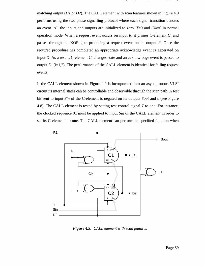
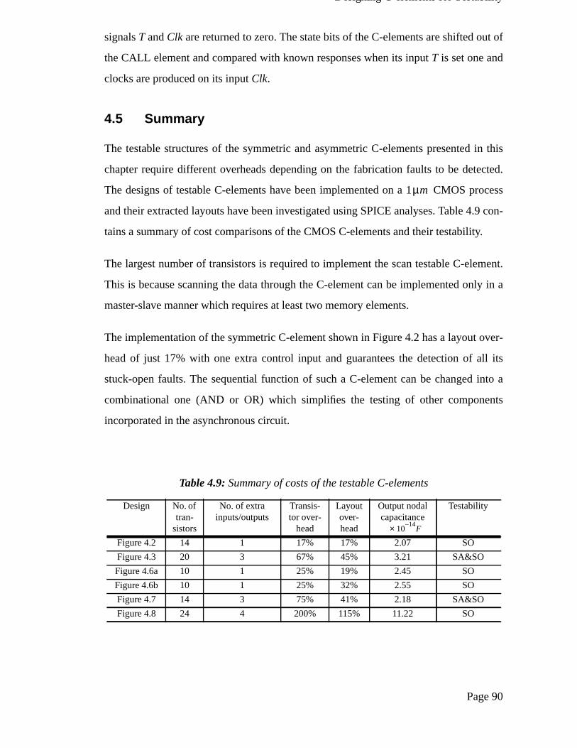
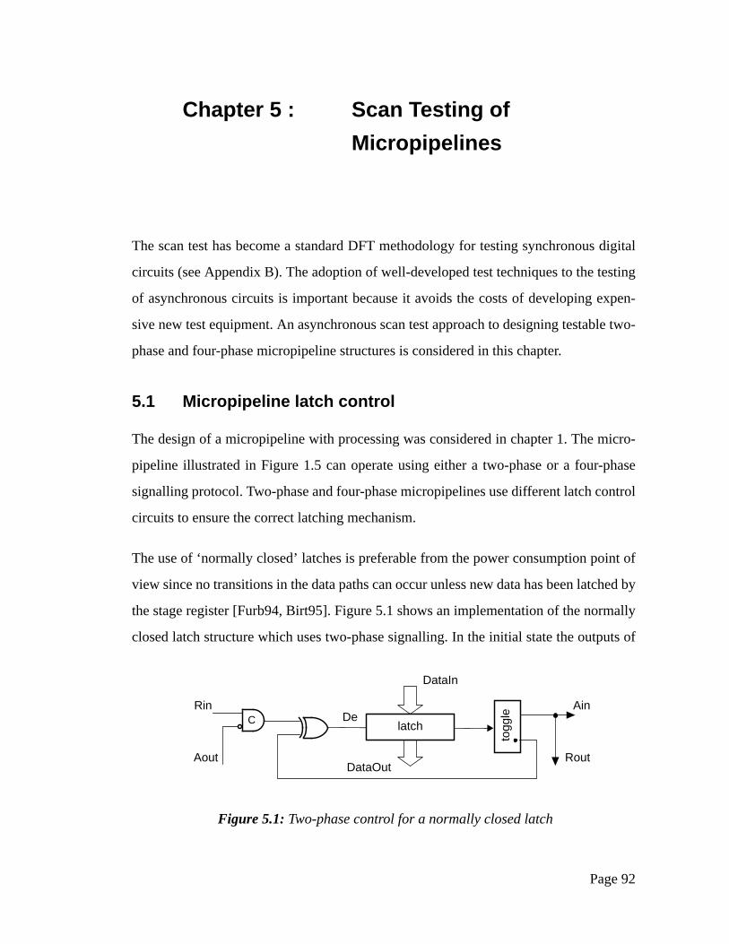
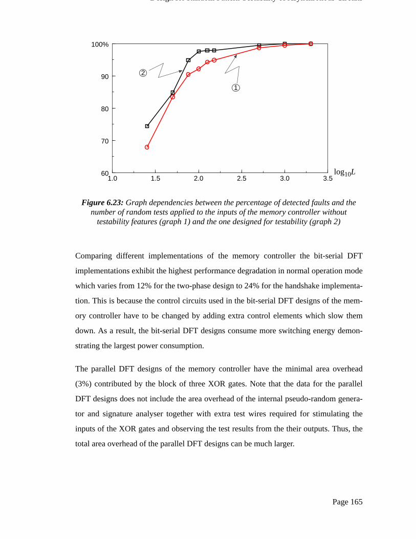
Design for Testability of Asynchronous VLSI Circuits A thesis submitted to the University of Manchester for the degree of Doctor of Philosophy in the Faculty of Science and Engineering Oleg Alexandrovich Petlin Department of Computer Science 1996
Transcript
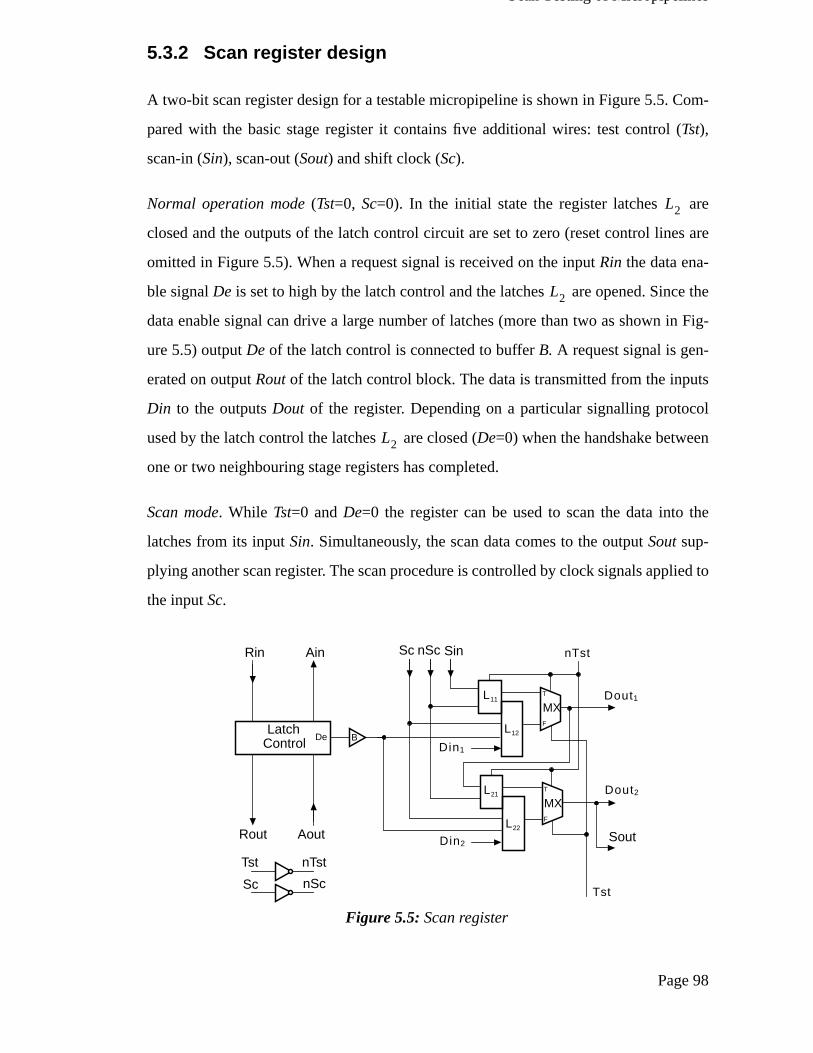
Design for Testability of
Asynchronous VLSI Circuits
A thesis submitted to
the University of Manchester
for the degree of
Doctor of Philosophy
in the Faculty of Science and Engineering
Oleg Alexandrovich Petlin
Department of Computer Science
1996
Page 2
Contents
Contents............................................................................................... 2List of Figures ..................................................................................... 7List of Tables..................................................................................... 12Abstract ............................................................................................. 14Declaration ........................................................................................ 15Copyright and the ownership of intellectual property rights............. 16Acknowledgements ........................................................................... 17The Author ........................................................................................ 18
1.3 Motivation for the chosen design methodologies................................... 281.4 Micropipelines........................................................................................ 29
3.1 Power consumption of CMOS circuits................................................... 583.2 Information theory and digital circuits ................................................... 593.3 Information content and transition probability....................................... 653.4 Discussion............................................................................................... 693.5 Summary................................................................................................. 70
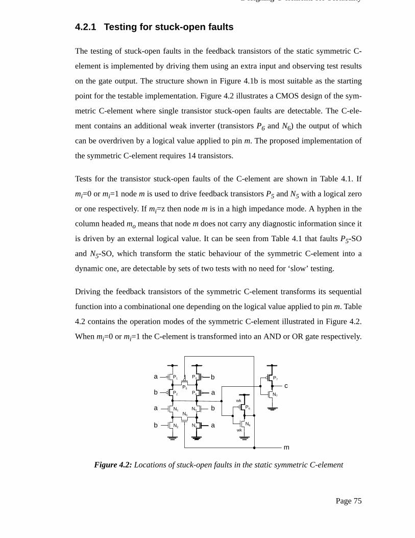
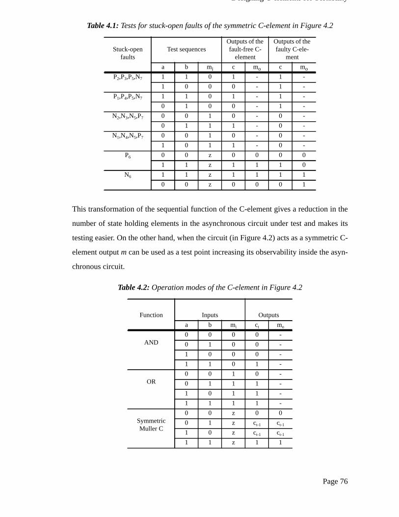
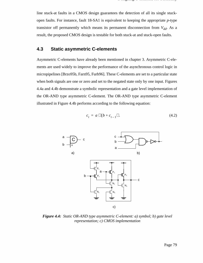
Chapter 4 : Designing C-elements for Testability............................ 72
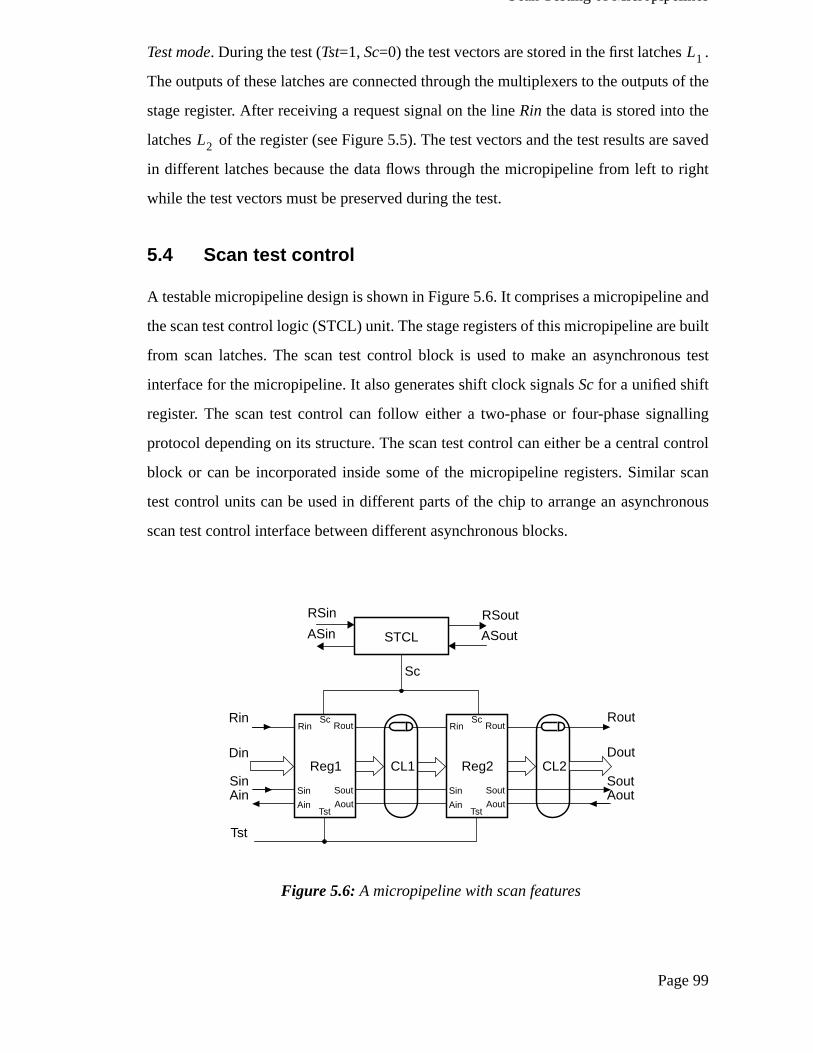
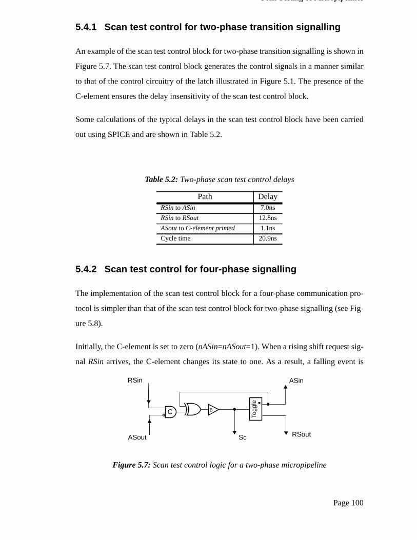
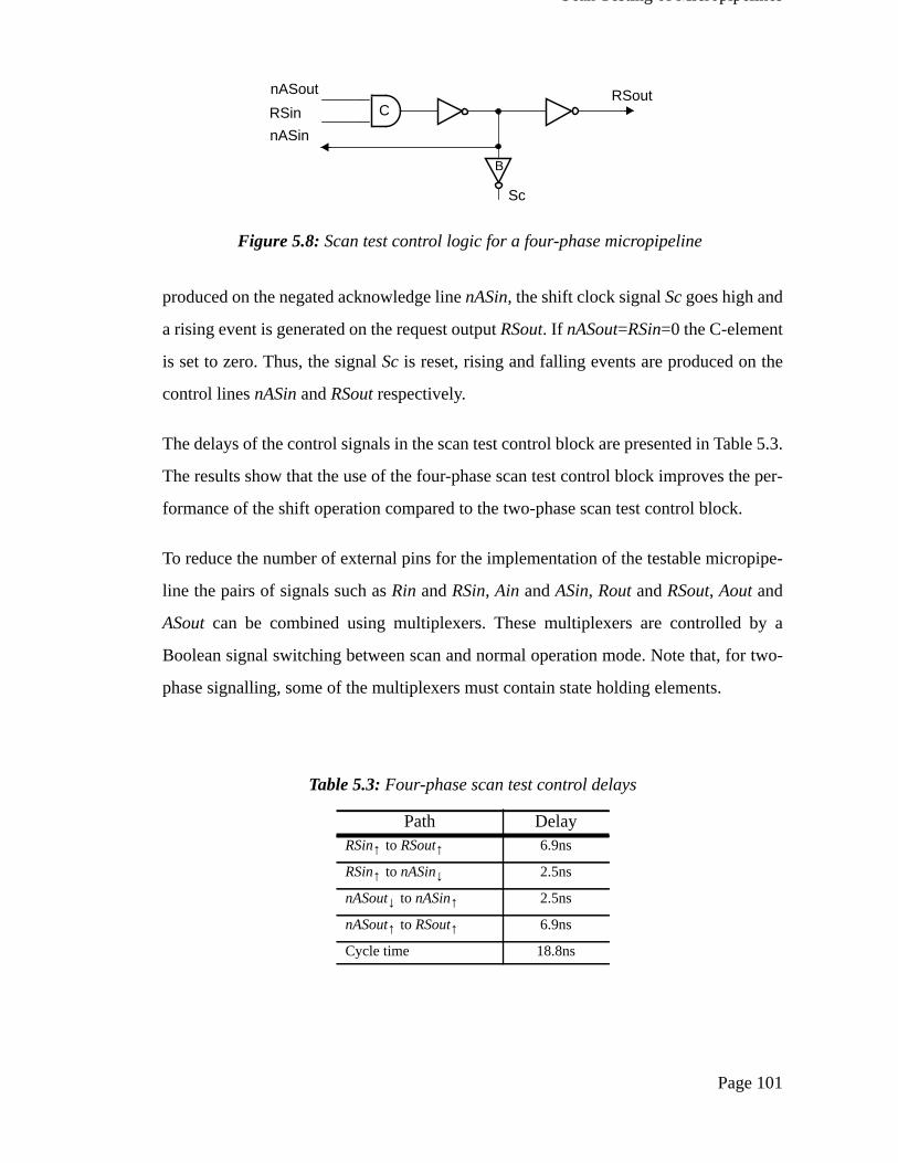
5.4 Scan test control ..................................................................................... 995.4.1 Scan test control for two-phase transition signalling..................... 1005.4.2 Scan test control for four-phase signalling .................................... 100
5.5 Test strategy.......................................................................................... 1025.6 Scan testing of asynchronous sequential circuits ................................. 106
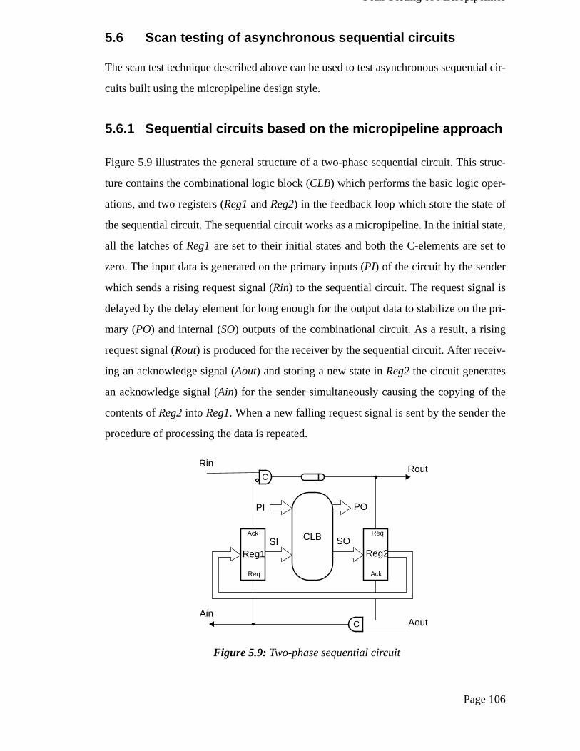
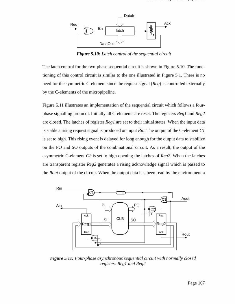
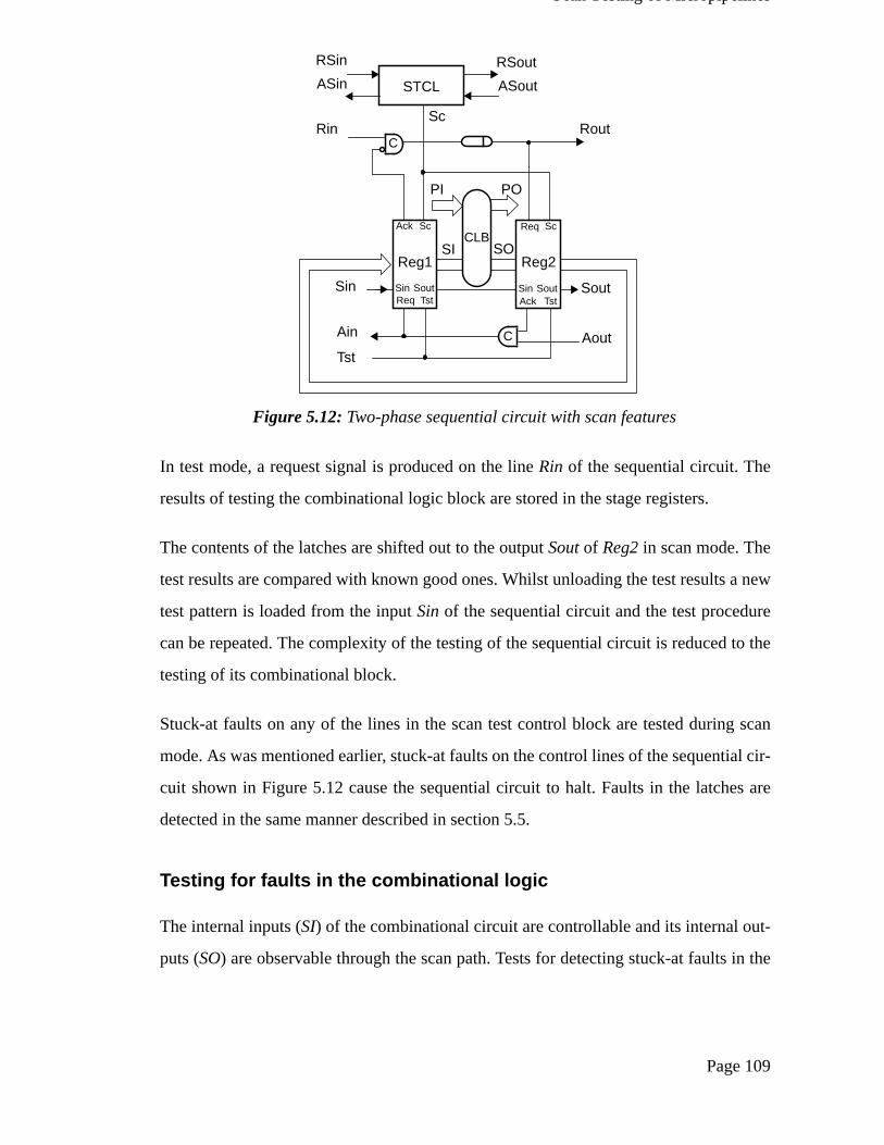
5.6.1 Sequential circuits based on the micropipeline approach.............. 1065.6.2 Scan test design.............................................................................. 1085.6.3 Scan test scenario........................................................................... 108
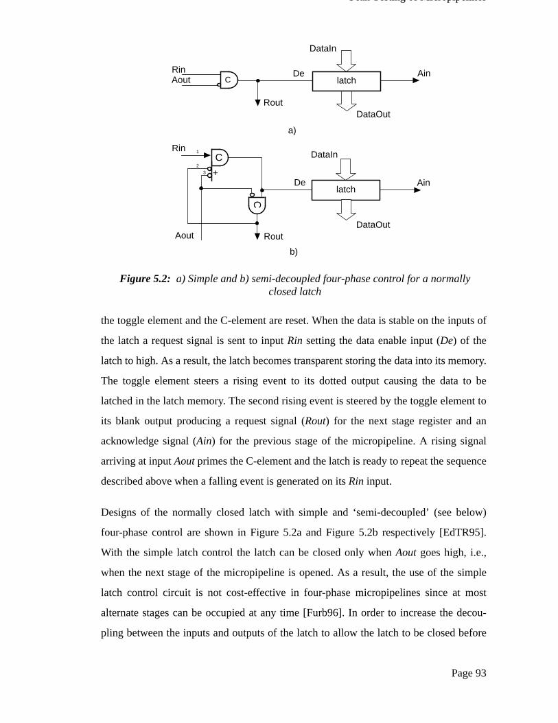
5.7 Testing faults in four-phase latch control circuits ................................ 111
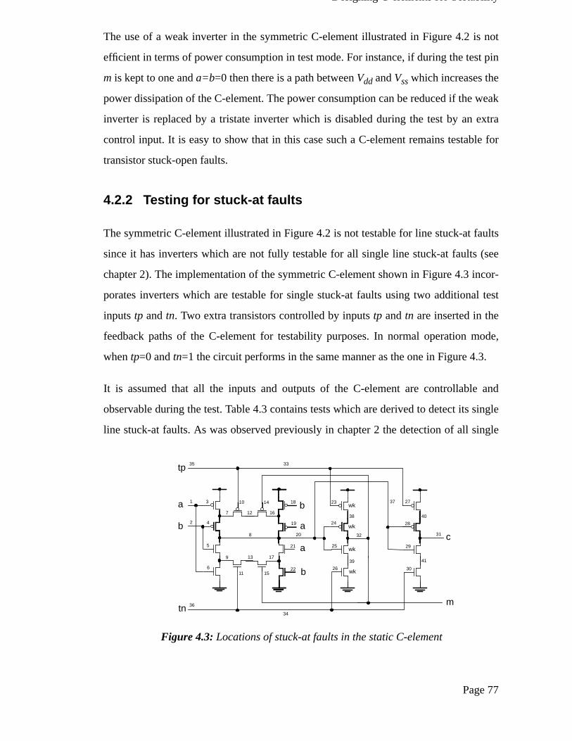
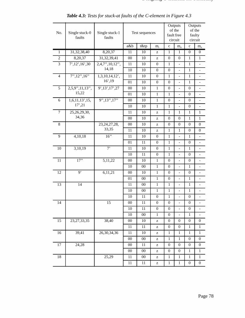
Contents
Page 4
5.7.1 Testing for faults in the semi-decoupled control circuit ................ 1115.7.2 Testing for faults in the control circuit of
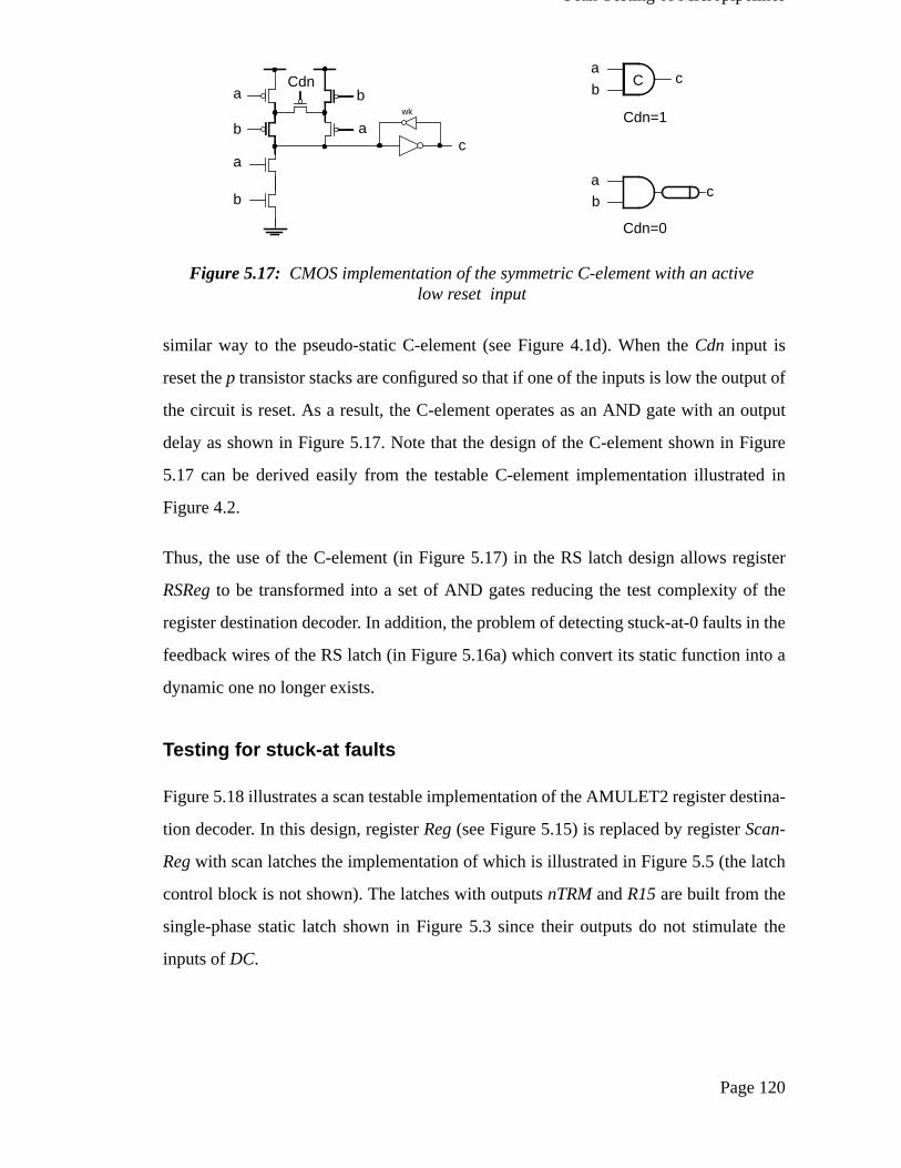
the four-phase sequential circuit ................................................... 1155.8 A case study of the AMULET2 register destination decoder............... 115
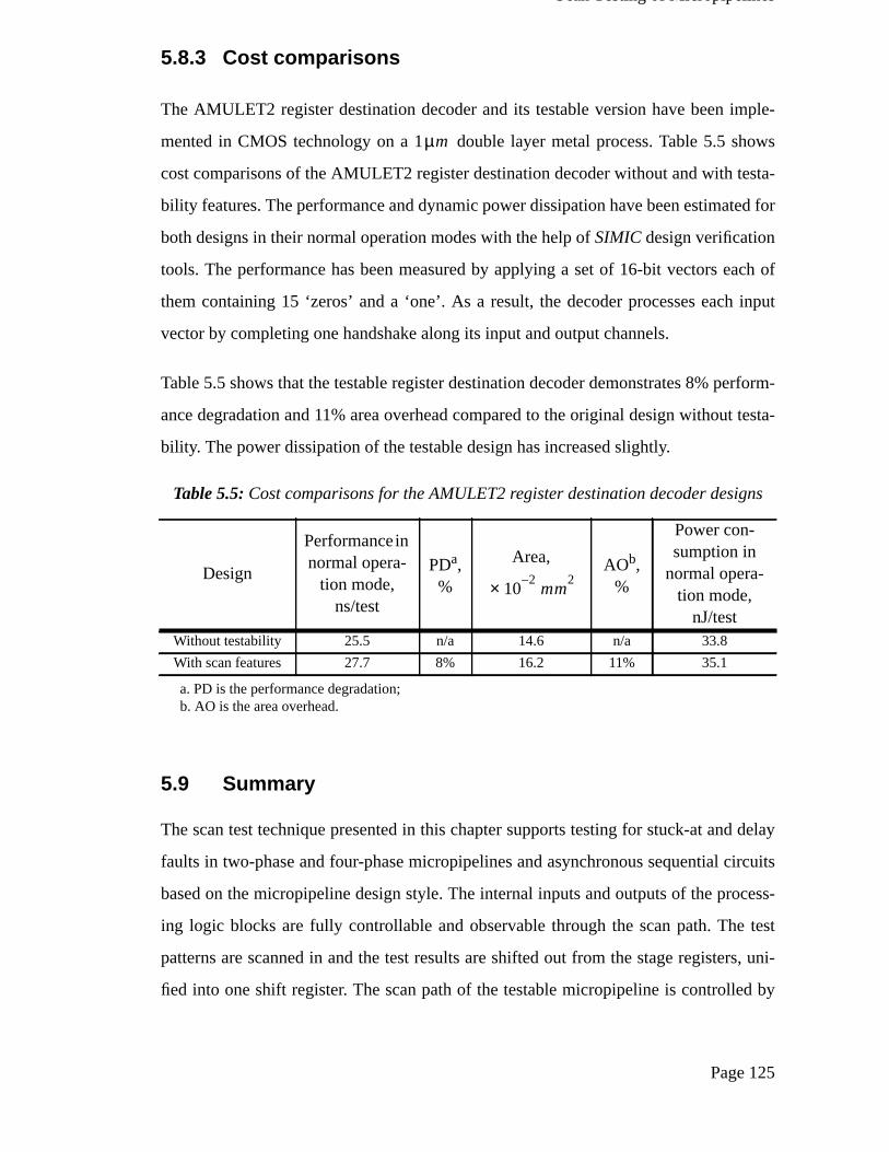
5.8.1 Design and implementation ........................................................... 1155.8.2 Design for testability...................................................................... 1185.8.3 Cost comparisons........................................................................... 125
6.2 Sequential circuit designs ..................................................................... 1346.3 Parallel random testing of sequential circuits....................................... 136
6.3.1 Probabilistic properties of an XOR gate........................................ 1366.3.2 Sequential circuit designs for random-pattern testability .............. 1366.3.3 Analysis of the parallel random testing technique......................... 141
6.4 Bit-serial random testing of sequential circuits .................................... 1416.4.1 Two-phase sequential circuit design.............................................. 1426.4.2 Four-phase sequential circuit design ............................................. 1466.4.3 Analysis of the bit-serial random test technique............................ 149
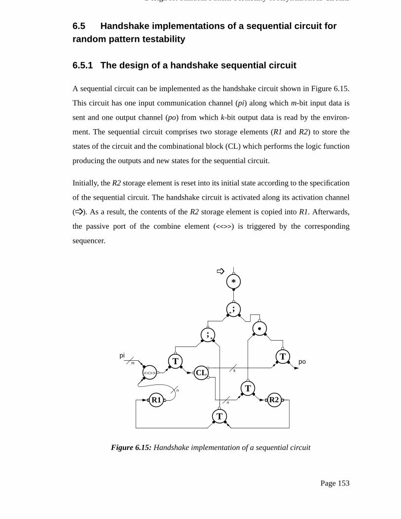
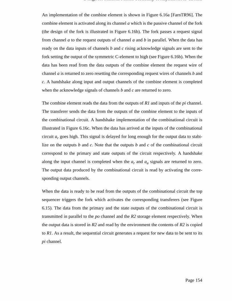
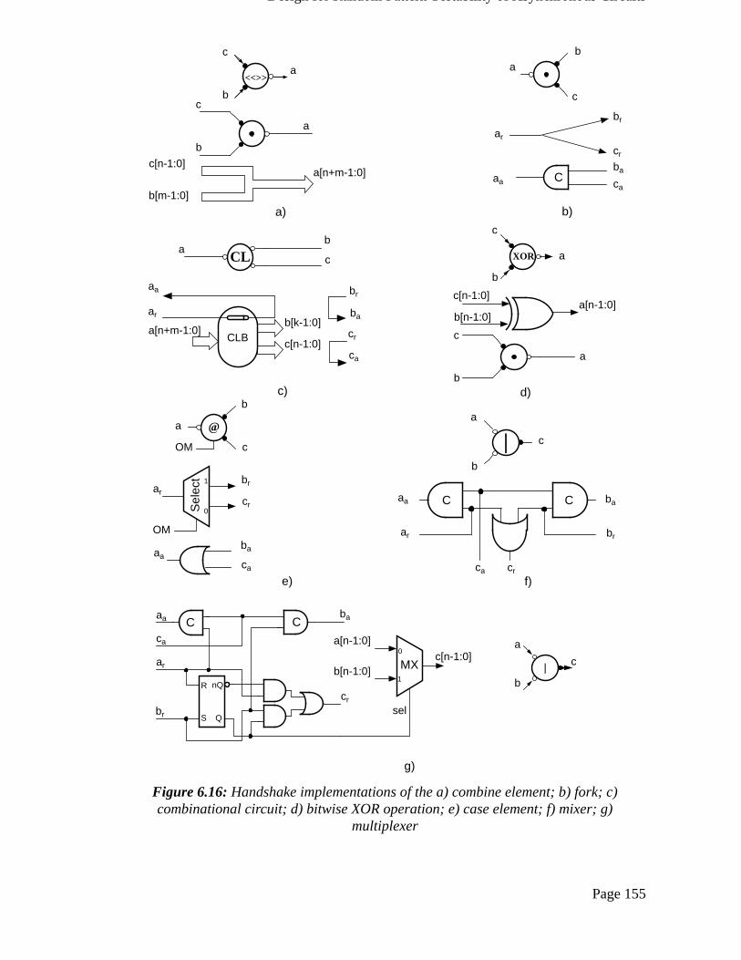
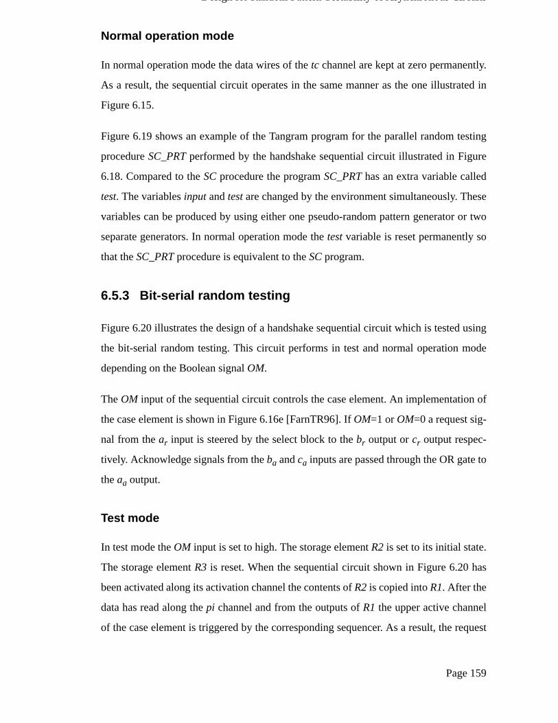
6.5 Handshake implementations of a sequential circuit for randompattern testability ...................................................................................153
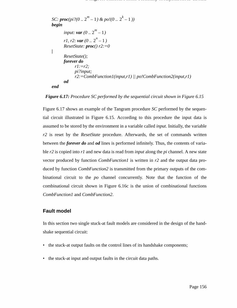
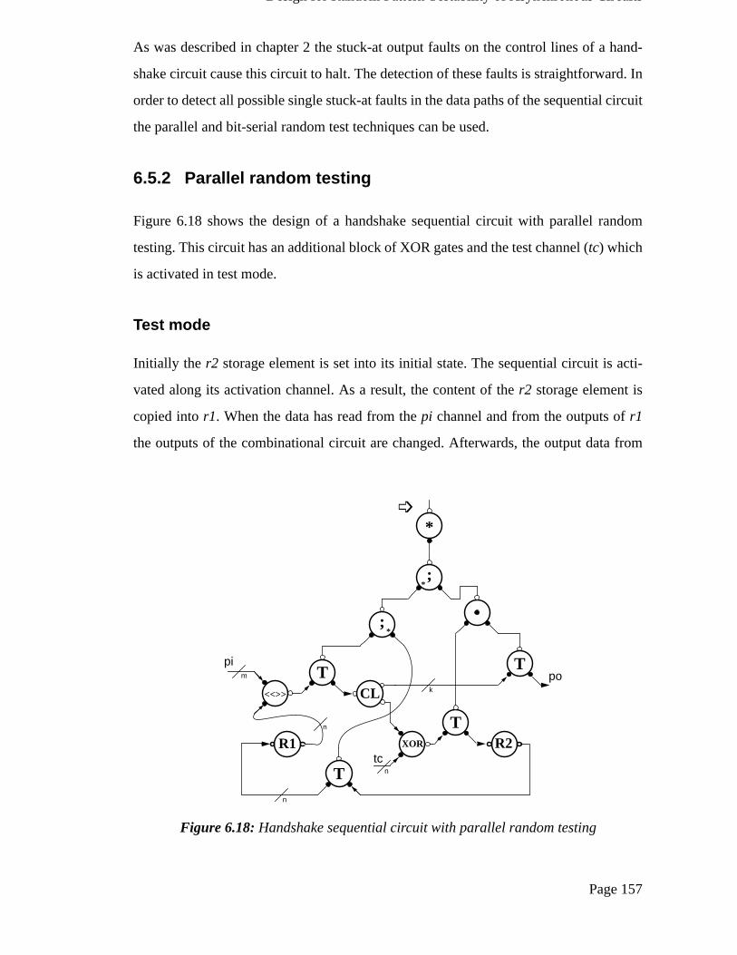
6.5.1 The design of a handshake sequential circuit ................................ 1536.5.2 Parallel random testing .................................................................. 1576.5.3 Bit-serial random testing................................................................ 159
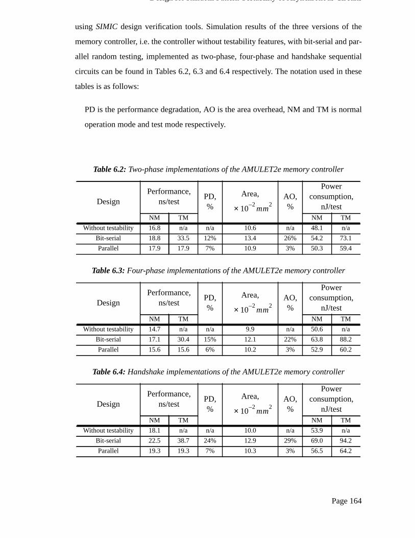
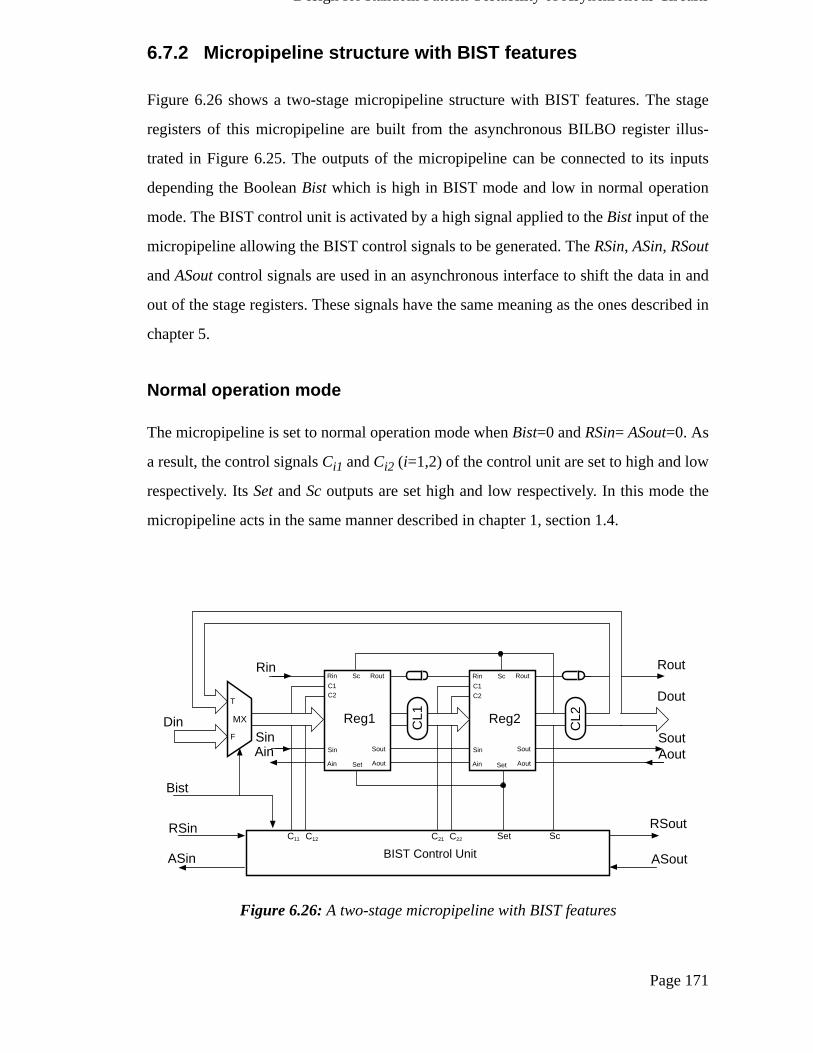
6.6 A case study of the AMULET2e memory controller ........................... 1636.7 Built-in self-testing of micropipelines.................................................. 167
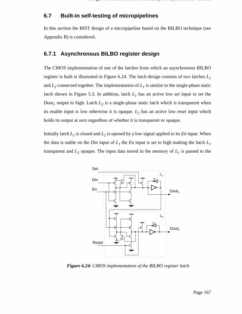
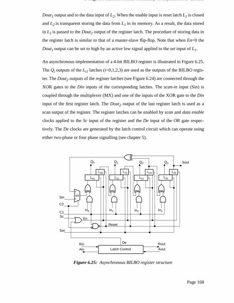
6.7.1 Asynchronous BILBO register design........................................... 1676.7.2 Micropipeline structure with BIST features .................................. 1716.7.3 Analysis of the BIST micropipeline structure ............................... 174
Chapter 7 : Design for Testability of an Asynchronous Adder...... 177
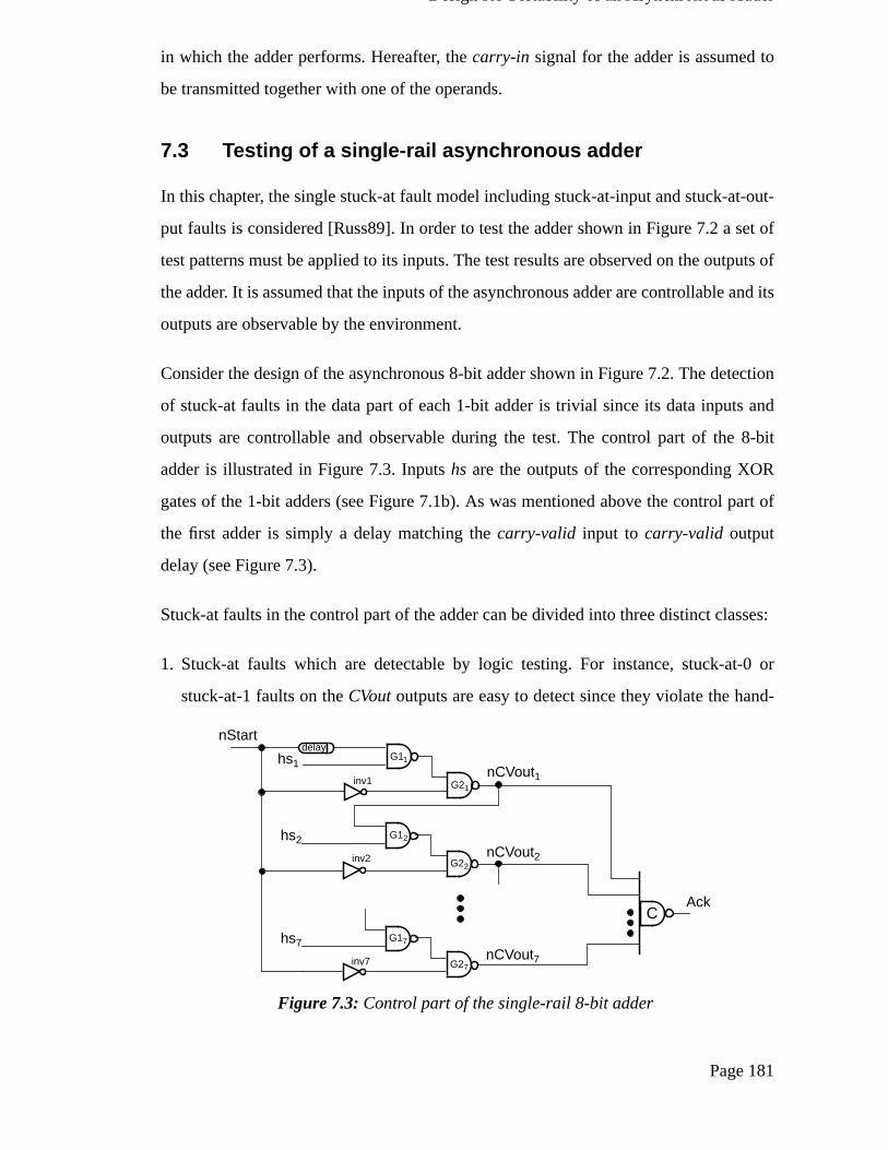
7.1 AMULET1 asynchronous adder........................................................... 1777.2 Single-rail asynchronous adder ............................................................ 1797.3 Testing of a single-rail asynchronous adder......................................... 181
7.3.1 Design for testability of the single-rail asynchronous adder ......... 183
Contents
Page 5
7.4 Dual-rail implementation of an asynchronous adder............................ 1867.5 Hybrid implementation of an asynchronous adder............................... 1887.6 A case study of an asynchronous comparator ...................................... 1907.7 Summary............................................................................................... 191
Chapter 8 : The Design and Test of an Asynchronous
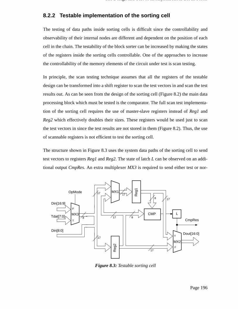
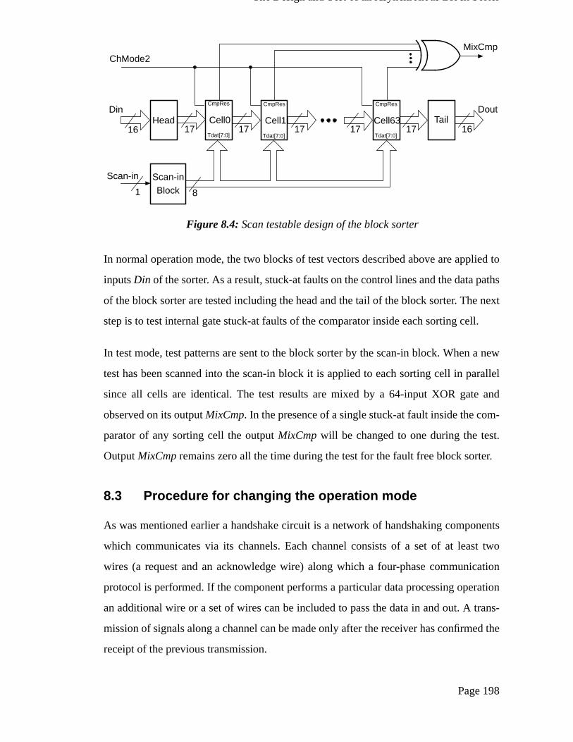
8.1 Design of the asynchronous block sorter.............................................. 1938.2 Testing the block sorter ........................................................................ 195
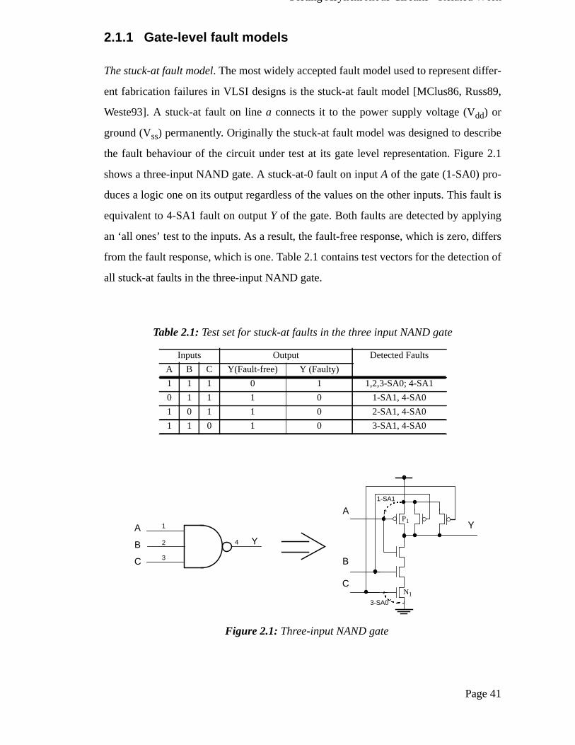
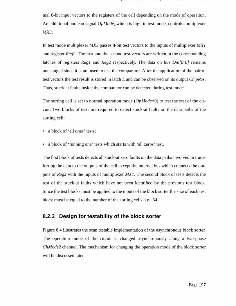
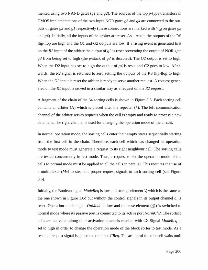
8.2.1 Fault model .................................................................................... 1958.2.2 Testable implementation of the sorting cell................................... 1968.2.3 Design for testability of the block sorter ....................................... 197
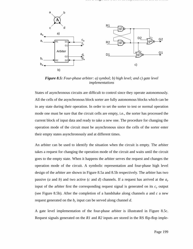
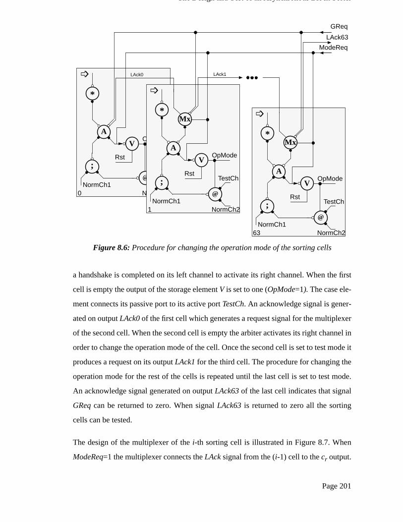
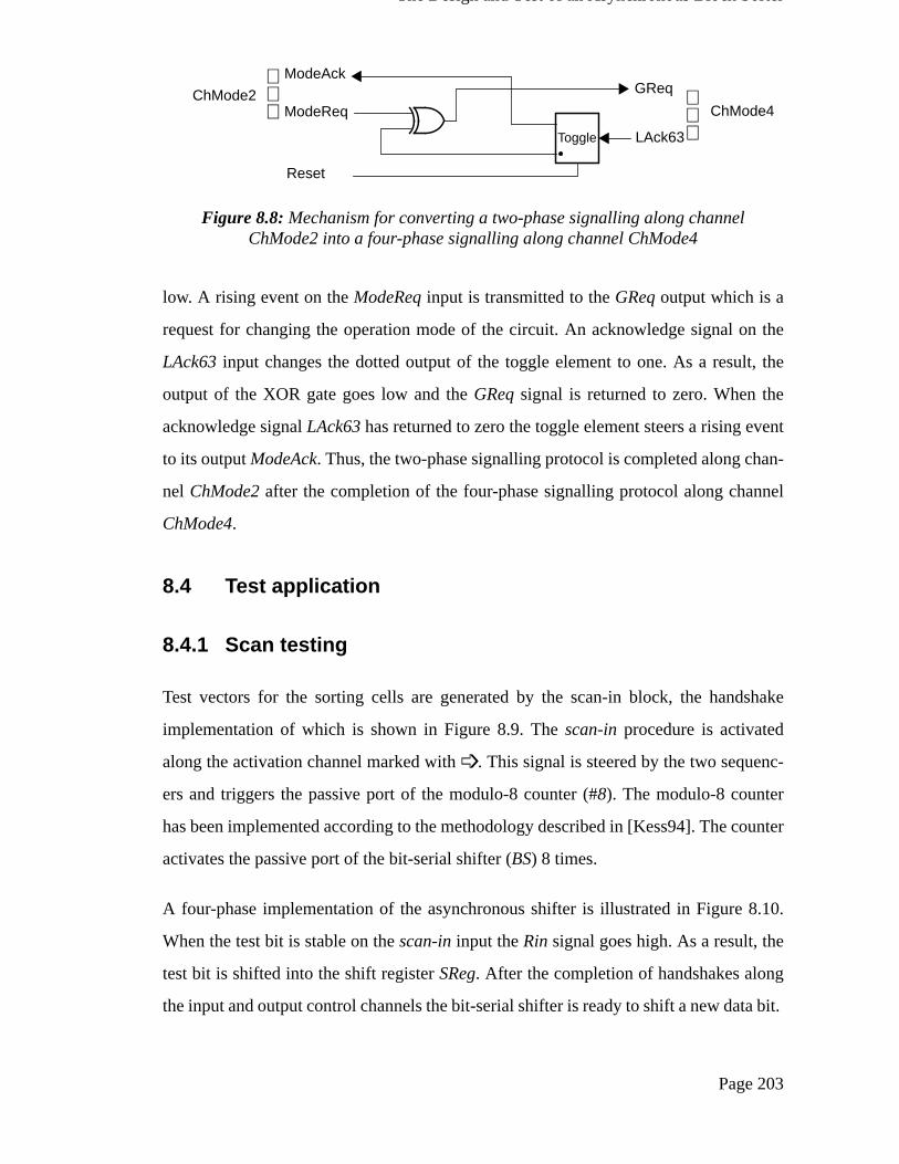
8.3 Procedure for changing the operation mode......................................... 1988.4 Test application .................................................................................... 203
Chapter 9 : Conclusions and Future Work ..................................... 210
9.1 Conclusions .......................................................................................... 2109.2 Future work .......................................................................................... 214
9.2.1 Testing control circuits .................................................................. 2149.2.2 Testing microprocessors ................................................................ 215
Appendix A : Testing of Synchronous VLSI Circuits ................... 216
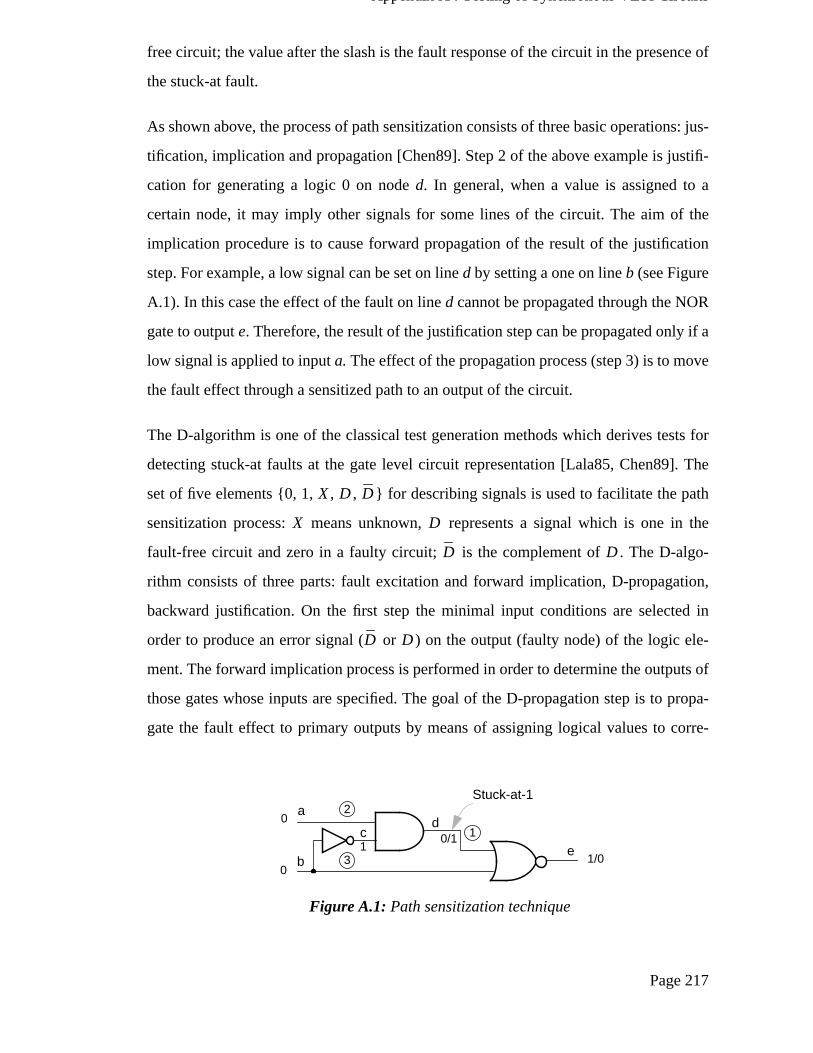
A.1 Test generation methods...................................................................... 216A.1.1 Algorithmic test generation .......................................................... 216A.1.2 Random pattern testing ................................................................. 218
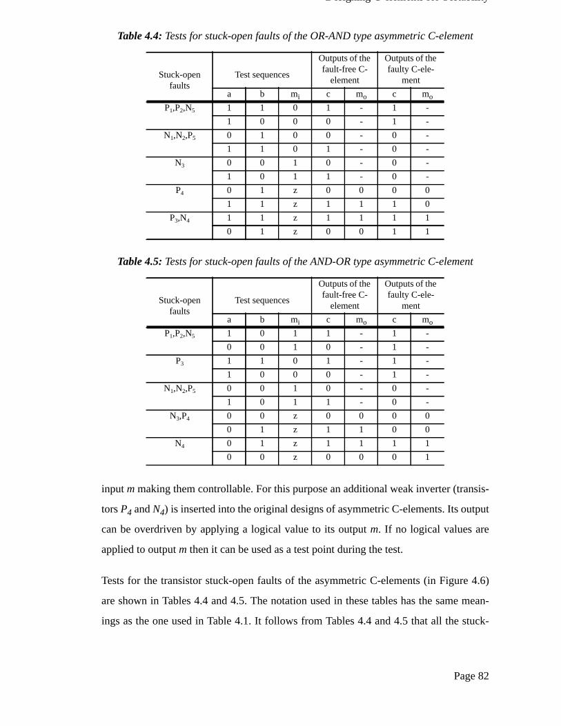
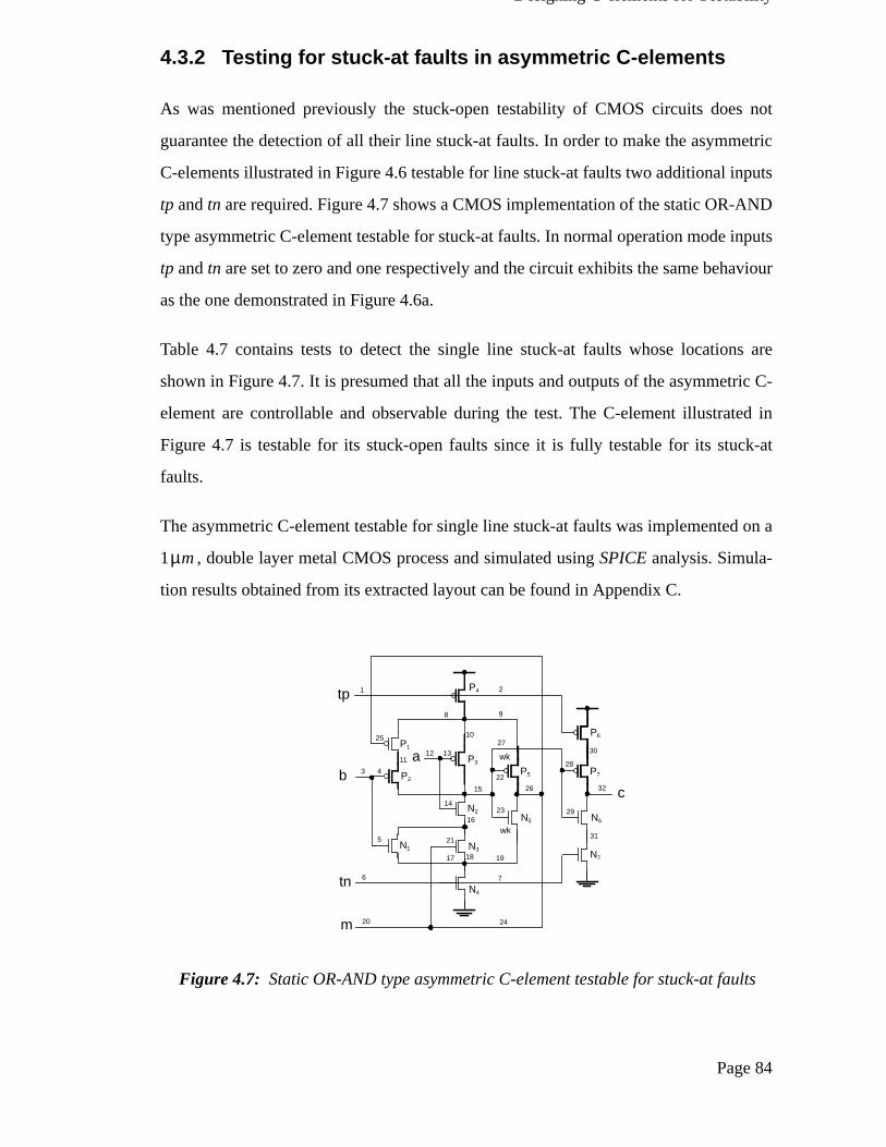
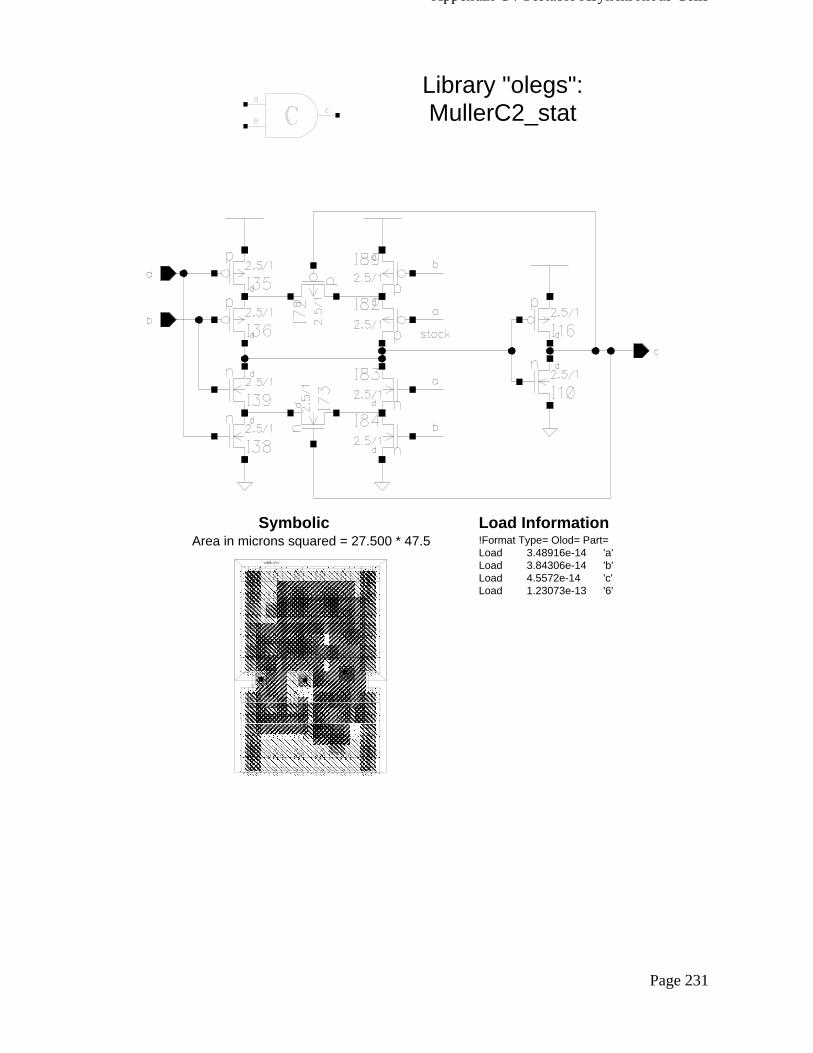
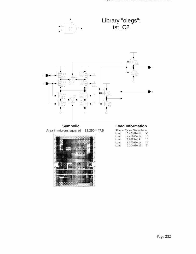
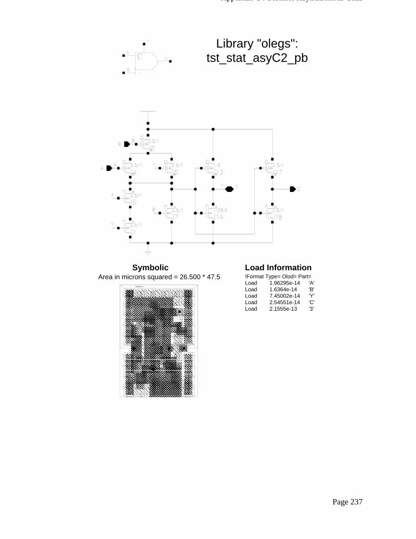
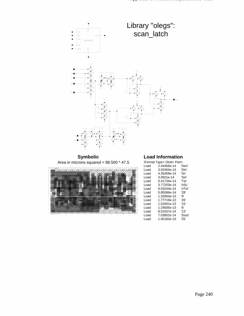
Appendix C : Testable Asynchronous Cells .................................. 230
Appendix D : AMULET2e memory controller.............................. 241
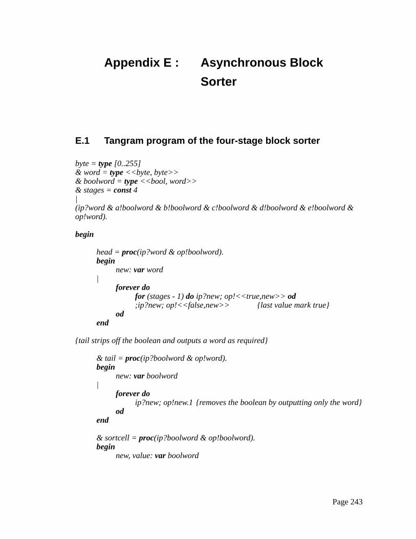
Appendix E : Asynchronous Block Sorter ..................................... 243
E.1 Tangram program of the four-stage block sorter ................................. 243E.2 Handshake implementations of the basic components of
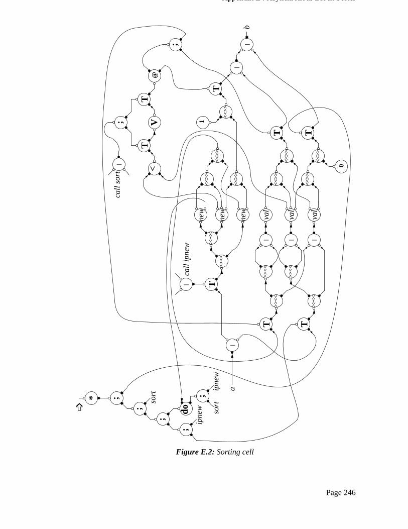
the block sorter .................................................................................... 245E.2.1 Handshake implementation of the head cell ................................. 245E.2.2 Handshake implementation of the sorting cell .............................. 245E.2.3 Handshake implementation of the tail cell .................................... 247
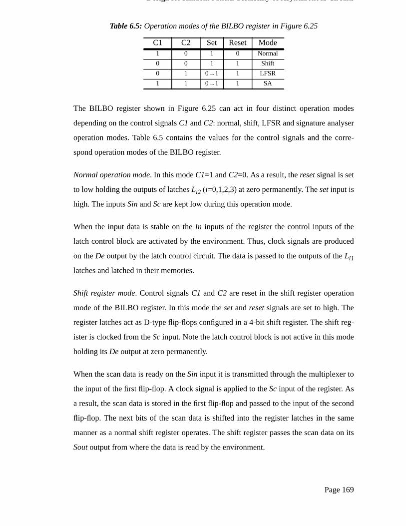
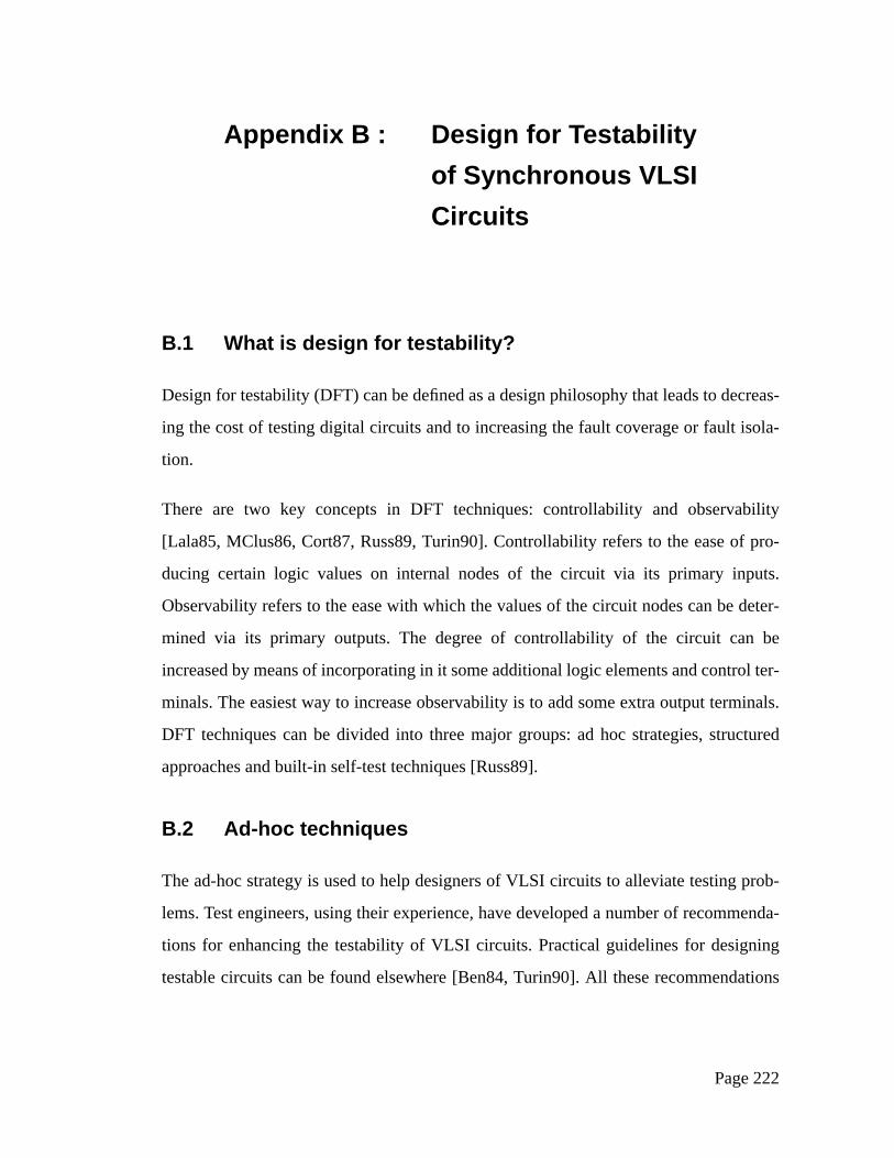
Table 6.5: Operation modes of the BILBO register in Figure 6.25...................169
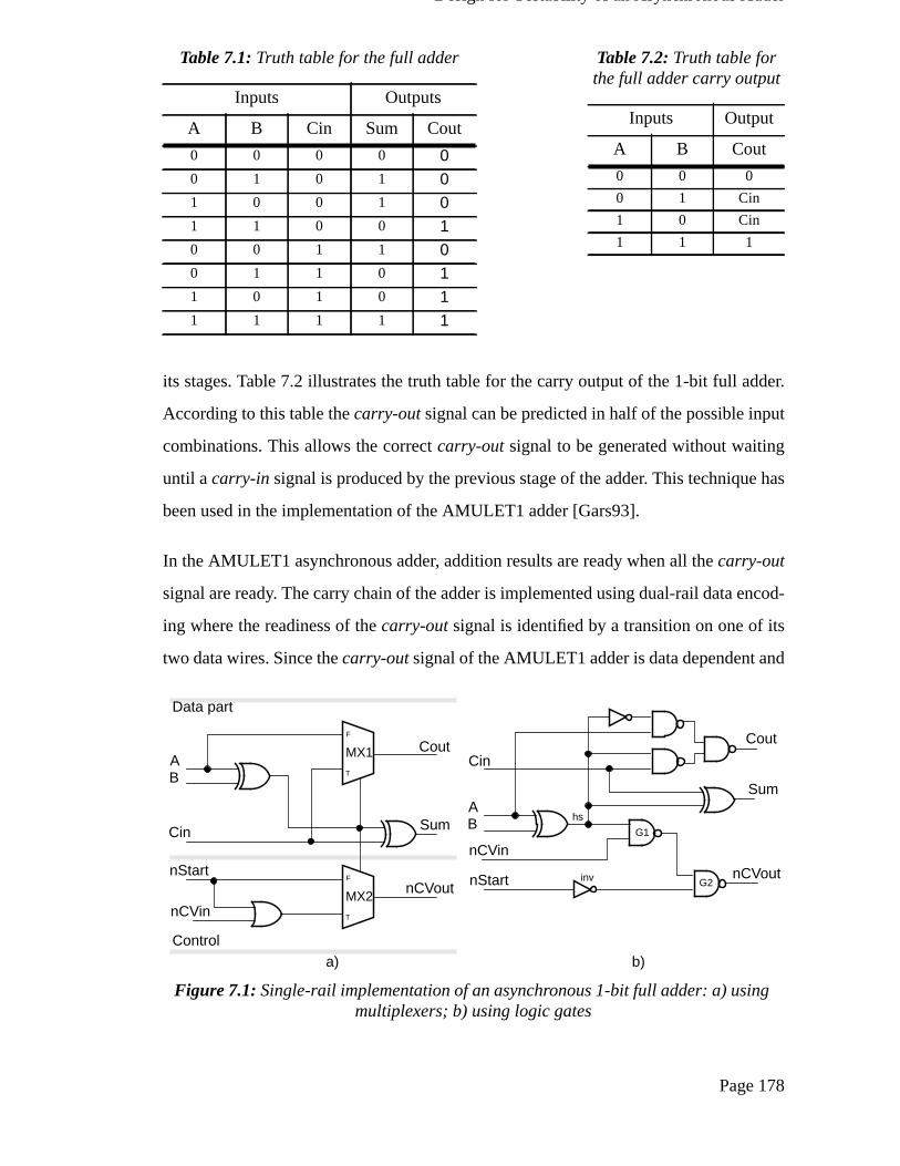
Table 7.1: Truth table for the full adder ............................................................178
Table 7.2: Truth table for the full adder carry output........................................178
Table 7.3: Simulation results of the comparator using
different adder designs .....................................................................192
Table 8.1: Simulation results and cost comparisons .........................................208
Table 9.1: Testability of micropipeline structures.............................................212
Table A.1: State sequence of the four-bit LFSR shown in Figure A.2b ........... 220
Table C.1: Names of the testable cells and their meanings .............................. 230
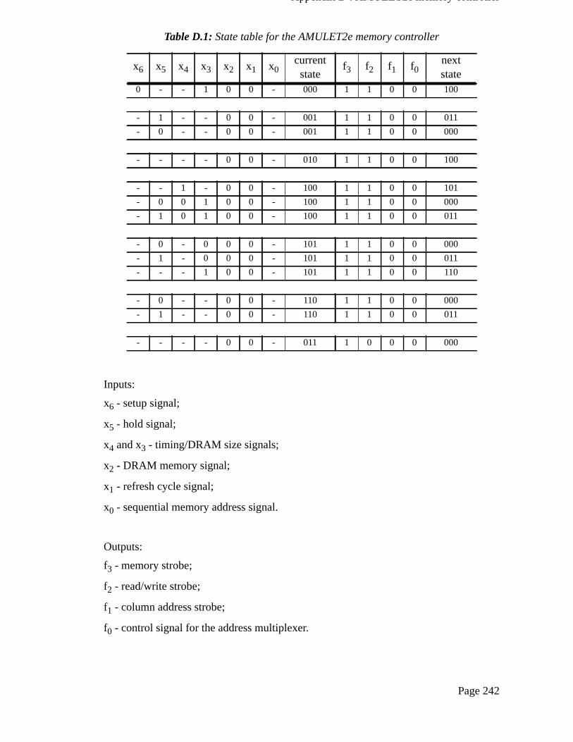
Table D.1: State table for the AMULET2e memory controller ........................ 241
Page 14
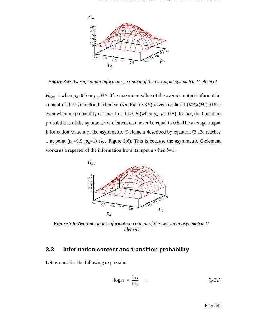
Abstract
Asynchronous design methodologies are a subject of growing research interest sincethey appear to offer benefits in low power applications and promise greater design mod-ularity. However, before these advantages can be exploited commercially, it must beshown that asynchronous circuits can be tested effectively in volume production. Thisthesis presents the results of research into various aspects of the design for testability ofasynchronous circuits.
Low power is often achieved by minimising circuit activity. However, testable designsrequire high transition probabilities. It is shown that design for testability and design forlow power are in direct conflict. As a result, the more testable a circuit is, the morepower it consumes. The resolution of this conflict can be found in the separation of nor-mal operation and test modes. In test mode the circuit activity is increased, dissipatingmore power.
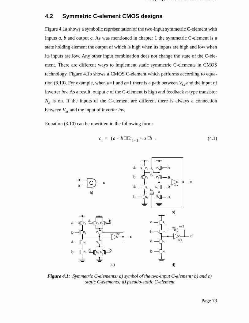
Many asynchronous designs use Muller C-elements in a large variety of applicationsincluding both control and data paths. Testable CMOS designs for C-elements are pre-sented which provide for the detection of transistor stuck-at and stuck-open faults.
The scan test technique is used to test stuck-at and delay faults in micropipelines. Thistechnique is generalised to the design for testability of either two-phase or four-phasemicropipelines. An asynchronous built-in self test (BIST) micropipeline design basedon the BILBO technique is presented. The proposed design for the BILBO registerallows stuck-at and delay faults to be detected inside the combinational circuits of themicropipeline.
Structural designs for random pattern testability techniques applicable to asynchronoussequential circuits are described. The proposed random test procedure provides for thedetection of all single stuck-at faults in the control and data paths of the sequential cir-cuit under test, reducing the overall test complexity to the testing of its combinationalnetwork.
Case studies of testable implementations of some high-level asynchronous functions,including an adder and a block sorter, are analysed for their testability, performance andarea cost. These designs show that, as expected, there is a trade-off to be made betweentestability and cost. However, satisfactory testability can be achieved for a circuitdesigned with a small area overhead for test circuitry and little performance degrada-tion.
Page 15
Declaration
No portion of the work referred to in this thesis has been submitted in support of an
application for another degree or qualification of this or any other university or institute
of learning.
Page 16
Copyright and the ownership of intellectual
property rights
Copyright in text of this thesis rests with the Author. Copies (by any process) either in
full, or of extracts, may be made only in accordance with instructions given by the
Author and lodged in the John Rylands University Library of Manchester. Details may
be obtained from the Librarian. This page must form part of any such copies made. Fur-
ther copies (by any process) of copies made in accordance with such instructions may
not be made without the permission (in writing) of the Author.
The ownership of any intellectual property rights which may be described in this thesis
is vested in the University of Manchester, subject to any prior agreements to the con-
trary, and may not be made available for use by third parties without the written permis-
sion of the University, which will prescribe the terms and conditions of any such
agreement.
Further information on the conditions under which disclosures and exploitation may
take place is available from the Head of Department of the Department of Computer
Science.
Page 17
Acknowledgements
During the years which I have spent in the Department of Computer Science at the Uni-
versity of Manchester I have received a great deal of help from many people, without
which the work described in this thesis would not have been achievable.
My supervisor Professor Steve Furber has been a great source of inspiration and moral
support. I would like to express my gratitude for his constant interest in my ideas and
research results and for correcting and commenting on drafts of this thesis.
The other members of the AMULET research group have created a friendly and com-
fortable atmosphere in which I have carried out my research. I am grateful to God that I
had the opportunity to conduct my research in the AMULET group which for me was a
rich source of ideas and vital material for the realization of my research results. I would
like to thank all of those people who have spent their valuable time to help me to under-
stand asynchronous VLSI design techniques.
I am especially grateful to Phil Endecott for his help and useful tips with theFrame-
Maker design environment. Many thanks to Craig Farnsworth whose invaluable practi-
cal recommendations and consultations with theCadence design environment and the
SIMIC design verification tools made it possible to implement my ideas in practice.
Some people have helped by reading and commenting on drafts of this thesis as well. I
must express my thanks to Phil Endecott and David Gilbert for their useful comments.
Page 18
The Author
Oleg Petlin obtained an Engineering degree (1989) and a Candidate of Technical Sci-
ences degree (1993) in Computer Science from Kiev Polytechnical Institute (Ukraine).
In 1994 he received a Master of Science degree in Computer Science from the Univer-
sity of Manchester.
This thesis is the result of three years of research as a member of the AMULET research
group at the University of Manchester. AMULET (Asynchronous Microprocessors
Using Low Energy Techniques) comprises several projects looking at different areas
where asynchronous logic techniques can be applied.
Page 19
To my mother
Page 20
Chapter 1 : Asynchronous VLSI
Circuits
This chapter starts by describing the major advantages of using asynchronous VLSI
designs and provides an overview of the asynchronous design methodologies and tech-
niques developed so far. Subsequent sections present descriptions of the micropipeline
and handshake circuit design methodologies which are the basic asynchronous design
styles used in the work described in this thesis. The importance of developing asynchro-
nous design for testability (DFT) techniques is discussed. Finally, the last section con-
tains a thesis overview describing the structure of this thesis and the results published by
the author.
1.1 Asynchronous VLSI circuits
Very Large Scale Integration (VLSI) circuits designed using modern Computer-Aided
Design (CAD) tools are becoming faster and larger, incorporating millions of smaller
transistors on a chip [Rice82, Russ87, Weste93]. VLSI designs can be divided into two
major classes: synchronous and asynchronous circuits. Synchronous circuits use global
clock signals which are distributed throughout their subcircuits to ensure correct timing
and to synchronize their data processing mechanisms. Asynchronous circuits contain no
global clocks. Their operation is controlled by locally generated signals [Mead80].
1.1.1 Motivation for using asynchronous circuits
A resurgence of interest in the design of asynchronous circuits has been stimulated by
their potential advantages compared to their synchronous counterparts:
• The absence of the clock skew problem. The largest problem with clocking in VLSI
circuits lies in distributing the clock at the same instant to all clocked elements across
Asynchronous VLSI Circuits
Page 21
the chip. “Clock skew” describes the phenomenon whereby different parts of the
VLSI system see the clock at slightly different times due to delay variations in the
clock interconnections. Clock distribution schemes which minimise the clock-skew
window become more and more costly in modern VLSI designs. This is because
modern state of art VLSI technology tends to use smaller transistors in larger chips
which increases the importance of physical delays along wires in a chip rather than
signal delays through transistors. For instance, the clock driver circuitry in the DEC
Alpha microprocessor occupies about 10% of the chip area [Dob93]. In asynchro-
nous circuits, the clock skew problem no longer exists since they do not use synchro-
nization clocks to control their operation.
• Performance. The fixed clock period in synchronous circuits is chosen using worst-
case performance analysis. As a consequence, synchronous circuits perform at their
worst-case rates. In asynchronous circuits, the communication between separate
blocks on the chip occurs when the data is ready to be transmitted. As a result, asyn-
chronous designs can exhibit typical case performance rather than worst-case per-
formance.
• Power consumption. The power consumption of VLSI circuits is important in porta-
ble digital systems since a design objective is to maximize the life of lightweight bat-
tery packs. All parts of a synchronous VLSI design are clocked even if they do not
produce “useful” results. In asynchronous circuits, only those parts of the circuit
which produce meaningful results are involved in the computation process. As a
result, the use of asynchronous circuits can lead to lower power consumption
[Birt95].
• Timing and design flexibility. If a synchronous VLSI circuit is required to work at a
higher clock frequency, all parts of the circuit must be improved to operate within the
shorter clock period. In an asynchronous circuit, performance can be enhanced by
modifying only the most active parts of the design using innovations in VLSI tech-
nology. Since asynchronous circuits communicate using signalling protocols rather
than clocks the modified components must only obey the requirements of the com-
Asynchronous VLSI Circuits
Page 22
munication protocol. In principal, greater throughput for synchronous circuits can be
achieved only when all VLSI components are realized on a new technology.
• Adoption to environmental variations. Changing environmental conditions can sig-
nificantly vary the logic delays in VLSI circuits. Synchronous circuits are simulated
extensively under a wide variation of parameters such as supply voltage and operat-
ing temperature to ensure that the chosen clock period guarantees correct operation
under all specified conditions. The adaptability of asynchronous VLSI circuits allows
them to function correctly under large environmental variations by allowing them to
operate more quickly or more slowly accordingly.
The advantages of asynchronous circuits have not yet been fully realised due to the fol-
lowing reasons:
• The design of asynchronous VLSI circuits for specific applications appears to be dif-
ficult due to the lack of suitable CAD tools.
• Special techniques for removing hazards in asynchronous circuits often lead to a sig-
nificant increase in silicon area [Lav93, Brzo95a].
Nevertheless, a growing interest from industry in asynchronous circuits is stimulating
research in design methodologies which can be used to develop efficient asynchronous
VLSI designs which could compete successfully in a market presently dominated by
synchronous circuits.
1.2 Asynchronous VLSI design methodologies
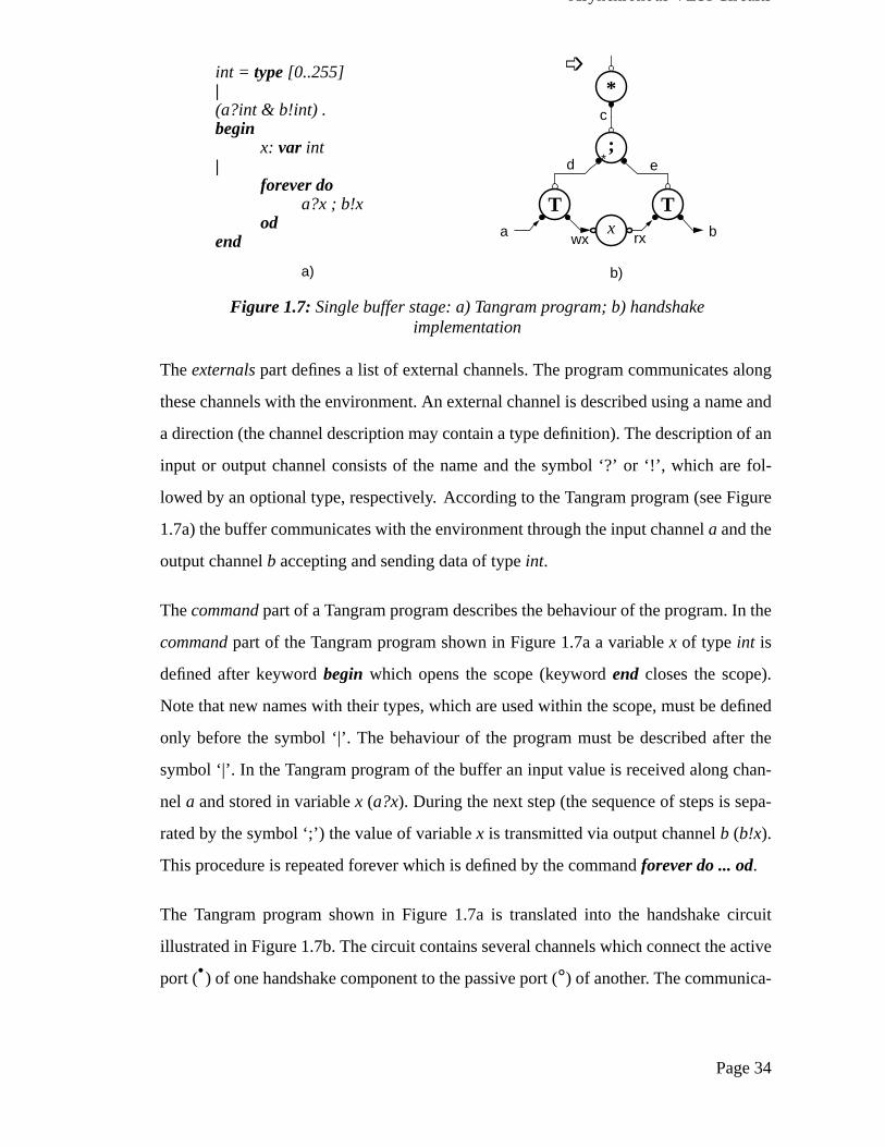
A large number of existing asynchronous design approaches can be classified using the
following three main criteria:
• delay models;
• data representation;
• signalling protocols.
Asynchronous VLSI Circuits
Page 23
1.2.1 Delay models in VLSI circuits
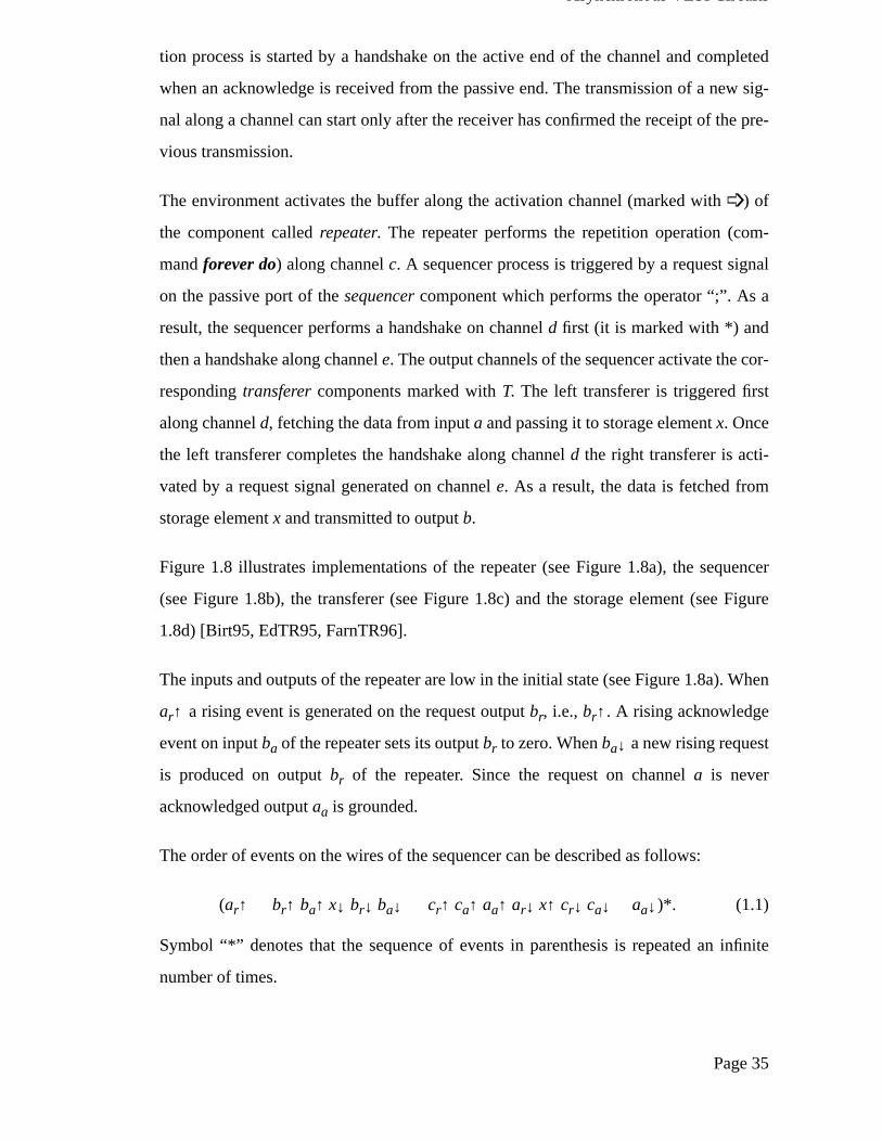
Delay models can be divided into three categories: fixed, bounded and unbounded delay
models. In the fixed delay model, the delay is assumed to have a fixed value. According
to the bounded delay model the delay may have any value in a given interval. In the
unbounded delay model, the delay can have any finite value. Delays in digital circuits
are associated with wires and gates. In principle, a circuit model is defined by its func-
tion and delay models for its wires and components [Birt95, Brzo95a].
Depending on the delay model assumption asynchronous circuits can be classified into
three major groups: delay-insensitive, speed-independent and bounded-delay circuits
[Birt95]:
• In delay-insensitive circuits all delays in gates and wires are allowed to be arbitrary
but finite.
• Gate delays inspeed-independent circuits are arbitrary and finite but signal transmis-
sions along wires are instantaneous. This assumption allows the use of the isochronic
fork [Berk91] where transitions on the forked parts arrive at their destinations at the
same time.
• A bounded-delay circuit uses the bounded delay model to ensure correct data
processing. In this model the delays through the data paths of the circuit are known
and bounded whereas the control logic remains delay-insensitive.
1.2.2 Data representation
Data in asynchronous circuits can be represented using either dual-rail or single-rail data
encoding.
Both delay-insensitive and speed-independent implementations require dual-rail encod-
ing of data where each data bit is represented by two wires: a “zero” propagation wire
Asynchronous VLSI Circuits
Page 24
and a “one” propagation wire. A standard level-sensitive dual-rail data encoding tech-
nique has four states:
• 00 - “initial state; data is not valid”;
• 10 - “transmission of a logical zero”;
• 01- “transmission of a logical one”;
• 11 - “illegal state”.
Once the data has been transmitted the wires must be returned to their initial state. Thus,
the presence of new data is indicated by a transition on one of the propagation wires.
The illegal state is not used in dual-rail data encoding.
The major disadvantage of using the dual-rail data representation compared to single-
rail data encoding, where each wire represents one bit of binary information, is that its
implementation requires twice as many wires and, as a consequence, leads to larger cir-
cuits. Bounded-delay asynchronous circuits allow the use of single-rail data encoding
where combinational logic circuits similar to those used in synchronous designs can be
used directly. This offers a significant reduction in silicon area.
1.2.3 Signalling protocols
Most asynchronous communications are based on using signalling protocols which
define a “handshake” procedure between two computation blocks [Berk93]. A typical
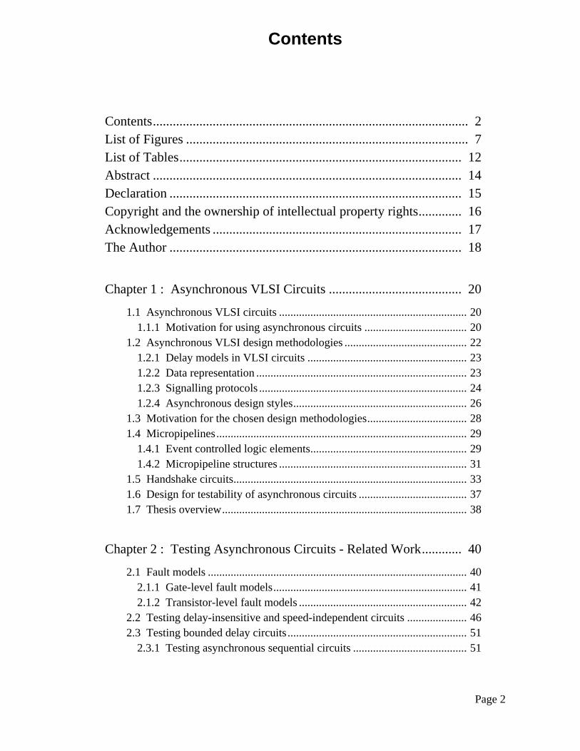
handshake protocol for a bundled-data system between a sender and a receiver is shown
SENDER RECEIVER
Request
Acknowledge
Data
Figure 1.1: Standard handshake signalling protocol
Asynchronous VLSI Circuits
Page 25
in Figure 1.1. According to this signalling scheme two control signals are required:
“request” and “acknowledge”. The request signal is used to initiate an action and the
acknowledge signal indicates the completion of the requested action. These control sig-
nals carry all the necessary timing information to provide for proper data communica-
tion. In the handshake protocol, there are always the initiator of the action which
generates the request and the passive circuit which waits for a request and then generates
the acknowledge. The full and empty circles in Figure 1.1 denote the active and the pas-
sive partners in the handshake procedure respectively.
Two transition signalling schemes can be used to implement an asynchronous signalling
protocol: two-phase (non-return to zero) and four-phase (return to zero) signalling
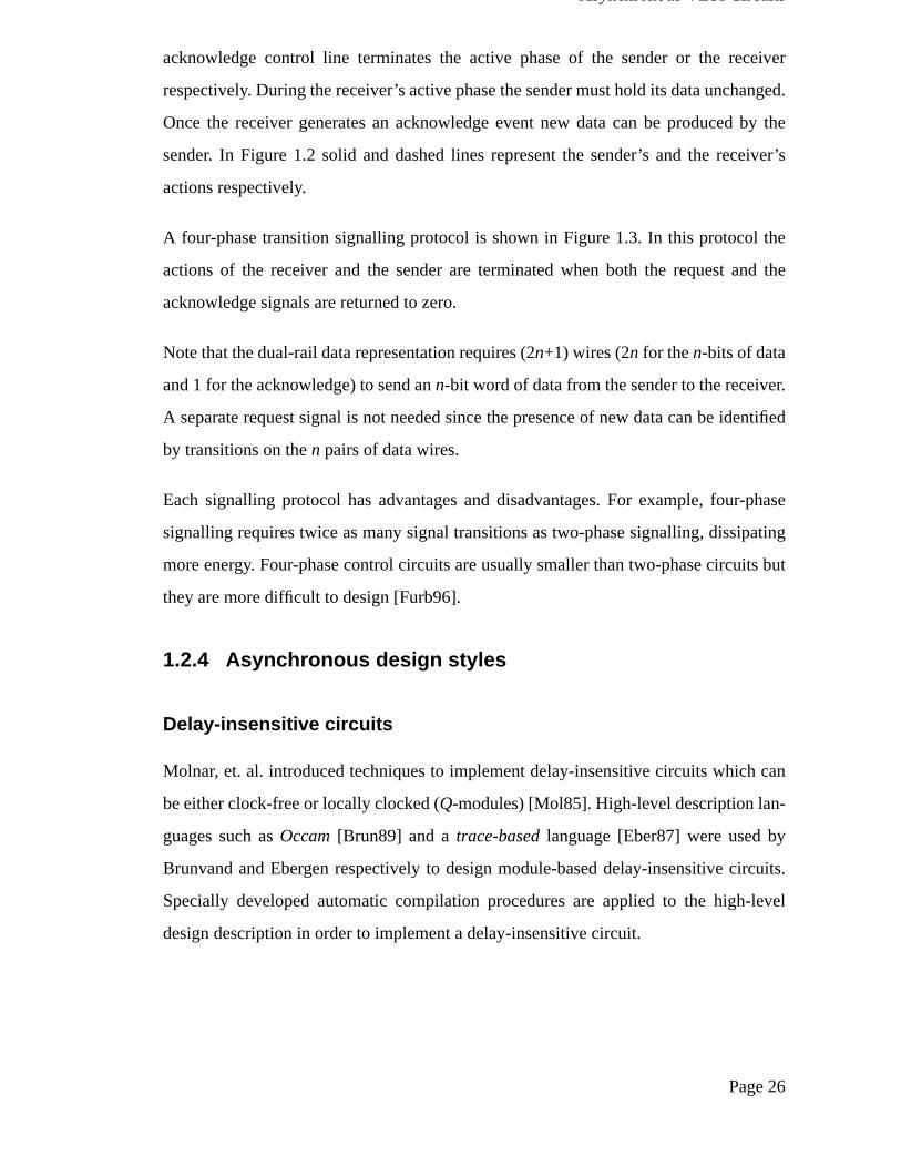
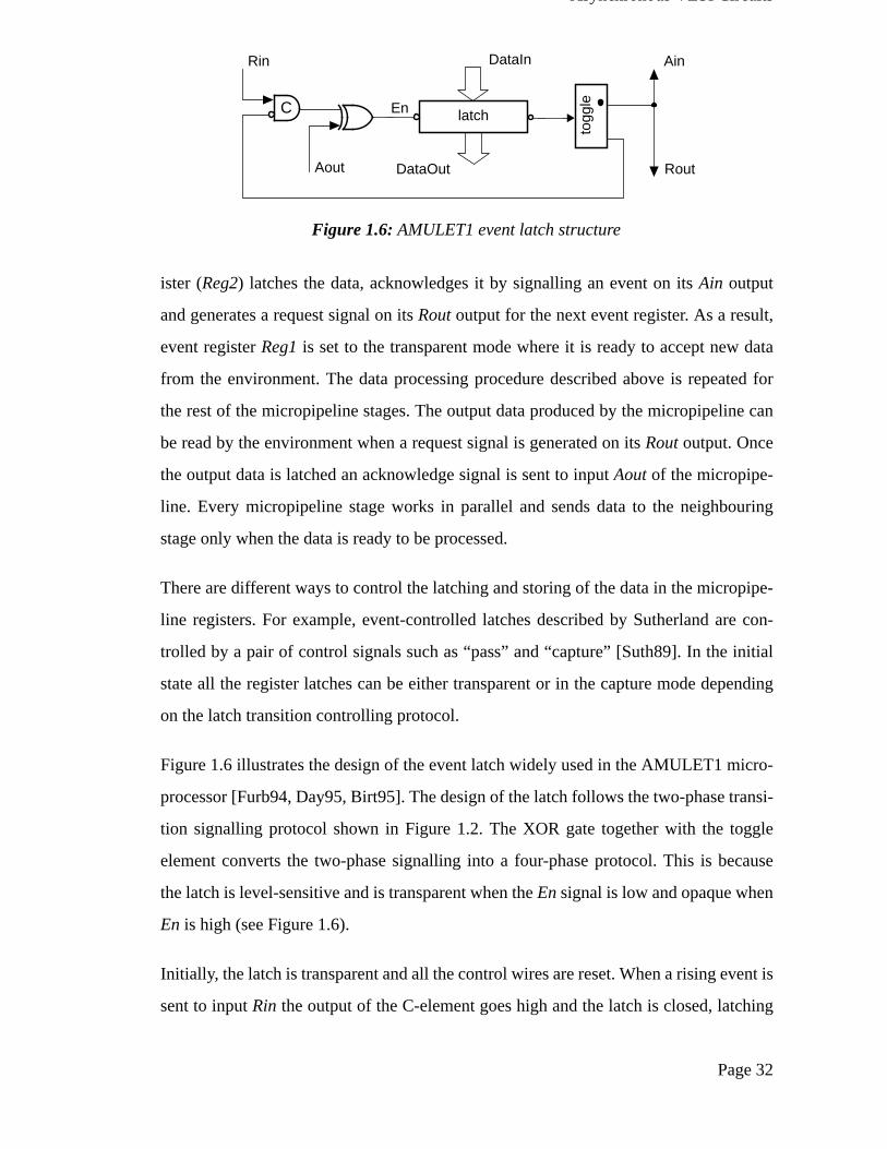
[Lav93, Birt95]. Figure 1.2 illustrates the two-phase bundled data signalling protocol.
There are two active phases in the communication process: the signal transitions (rising
or falling) on the request and acknowledge wires. An event on the request or the
Figure 1.2: Bundled-data protocol using two-phase transition signalling
Data
Acknowledge
Request
sender’s action receiver’s action
Figure 1.3: Bundled-data protocol using four-phase transition signalling
Request
Data
Acknowledge
Asynchronous VLSI Circuits
Page 26
acknowledge control line terminates the active phase of the sender or the receiver
respectively. During the receiver’s active phase the sender must hold its data unchanged.
Once the receiver generates an acknowledge event new data can be produced by the
sender. In Figure 1.2 solid and dashed lines represent the sender’s and the receiver’s
actions respectively.
A four-phase transition signalling protocol is shown in Figure 1.3. In this protocol the
actions of the receiver and the sender are terminated when both the request and the
acknowledge signals are returned to zero.
Note that the dual-rail data representation requires (2n+1) wires (2n for then-bits of data
and 1 for the acknowledge) to send ann-bit word of data from the sender to the receiver.
A separate request signal is not needed since the presence of new data can be identified
by transitions on then pairs of data wires.
Each signalling protocol has advantages and disadvantages. For example, four-phase
signalling requires twice as many signal transitions as two-phase signalling, dissipating
more energy. Four-phase control circuits are usually smaller than two-phase circuits but
they are more difficult to design [Furb96].
1.2.4 Asynchronous design styles
Delay-insensitive circuits
Molnar, et. al. introduced techniques to implement delay-insensitive circuits which can
be either clock-free or locally clocked (Q-modules) [Mol85]. High-level description lan-
guages such asOccam [Brun89] and atrace-based language [Eber87] were used by
Brunvand and Ebergen respectively to design module-based delay-insensitive circuits.
Specially developed automatic compilation procedures are applied to the high-level
design description in order to implement a delay-insensitive circuit.
Asynchronous VLSI Circuits
Page 27
Quasi delay-insensitive and speed-independent circuits
Martin proposed a methodology for designing so calledquasi delay-insensitive circuits
which differ from speed-independent circuits mainly in the assumption that all forks in
speed-independent circuits are isochronic, whereas quasi delay-insensitive circuits
allow forks to be either isochronic or delay-insensitive. The design process includes two
main steps:
• the developing of the high-level specification using thecommunicating sequential
processes (CSP) [Mart90] language;
• the translation of the high-level specification into a circuit implementation.
Philips research laboratories developed theTangram programming language which is
similar to CSP. A set of tools providing for the compilation of the Tangram program in a
handshake circuit has been implemented [Berk88, Berk91].
Several reports proposed a number of design techniques for speed-independent circuits
[Chu87, Meng89]. These design approaches are based on the high-level circuit specifi-
cation in the form of signal transition graph (STG).
Bounded-delay circuits
Bounded-delay circuits use thefundamental-mode assumption that the environment
must wait for long enough for the output data to stabilize on the circuit outputs. The
principles of fundamental-mode design techniques were developed first by Huffman
[Huff54] and later extended by Unger [Unger69].
A design approach to buildingburst-mode finite state machines was proposed by
Nowick et al. [Nowick91]. According to this approach:
• each state transition can occur under a certain set of input changes (so called aninput
burst) so that no burst from a particular state can be a subset of another burst from the
same state;
Asynchronous VLSI Circuits
Page 28
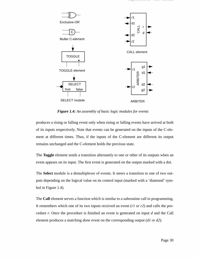
• any state must be entered with the same set of input values.
The proposed timing mechanism allows the burst-mode finite state machine to be
moved to a new state whenever the output associated with the previous state has
changed enabling the input signals to be changed.
Ivan Sutherland in his 1988 Turing Award lecture described an elegant approach to
building asynchronous pipelines called micropipelines [Suth89]. Micropipelines are
asynchronous, event-driven pipelines based on the bundled-data interface. In micropipe-
lines, the data is treated as a bundle, i.e. when the data produced by the sender is stable
the sender issues a request event to the receiver; the receiver acknowledges the receipt
of the data by sending an acknowledge event (see Figures 1.2 and 1.3). This handshak-
ing mechanism is repeated when further data is produced by the sender.
1.3 Motivation for the chosen design methodologies
As has been shown above there is a great variety of different asynchronous design tech-
niques. In this thesis the micropipeline and handshake circuit design methodologies are
considered for the following reasons:
• An asynchronous version of the ARM6 microprocessor (AMULET1) has been
designed by the AMULET research group at the Department of Computer Science in
the University of Manchester and fabricated by GEC Plessey Semiconductors Lim-
ited. AMULET1 was designed using the micropipeline design approach with two-
phase signalling which offers a good engineering framework for the design of com-
plex asynchronous VLSI circuits [Furb94, Pav94]. A second generation of asynchro-
nous ARM microprocessor called AMULET2 has recently been designed by the
AMULET group. The design of the AMULET2 microprocessor is based on the four-
phase micropipeline framework [Furb96].
• A great deal of engineering work has been carried out in the AMULET group to opti-
mise the design flow of asynchronous circuits initially described in the Tangram lan-
guage [Farn95, EdTR95]. In collaboration with Philips Research Laboratories an
Asynchronous VLSI Circuits
Page 29
effective design environment has been developed and incorporated within the
Clearly, both the pseudo-random pattern generator, which is used to generate stimulus
for the circuit under test, and the signature analyser, which collects the test results, must
operate asynchronously following the signalling protocol of the test object. The designs
of the asynchronous pseudo-random generator and signature analyser can be imple-
Design for Random Pattern Testability of Asynchronous Circuits
Page 128
mented using the corresponding synchronous LFSR and signature analyser described in
Appendix A. Figures 6.1a and 6.1b illustrate the design of an asynchronous LFSR and
signature analyser respectively. Both the synchronous LFSR in Figure 6.1a and the syn-
chronous signature analyser in Figure 6.1b are clocked by the latch control circuits
which can follow either two-phase or four-phase signalling. The two-phase latch control
circuit can be implemented using the circuit shown in Figure 5.1. An example of the
four-phase latch control circuit is shown Figure 6.2. TheRin signal is buffered to guar-
antee the required drive strength of the clock signal (Clk). TheRout andAout signals or
the Rin andAin signals in the latch control circuits of the asynchronous signature ana-
lyser or LFSR can be used by the environment to calculate the number of test vectors
applied to the circuit under test respectively.
Note that the synchronous LFSR and a signature analyser are built using shift registers
with master-slave flip-flops. This allows two different data latching schemes to be used
in four-phase signalling. According to the first data latching scheme the input data must
be stable beforeRin goes high untilAout is set to high. In the second data latching
Figure 6.1: Asynchronous a) pseudo-random pattern generator; b) signatureanalyser based on a synchronous LFSR
LFSR
Rin
Ain
n
Out
Rst
Rst
LatchControl
Rout
Aout
Synch
a)
SA
Rin
Ain
n
Out
Rst
Rst
LatchControl
Rout
Aout
Synch
b)
m
In
Clk Clk
Figure 6.2: Four-phase latch control
Rin
Ain
BRout
Aout
Clk
Design for Random Pattern Testability of Asynchronous Circuits
Page 129
scheme the input data must be stable until a handshake is completed along the input (Rin
andAin control wires) and output channels (Rout andAout control wires), i.e., all the
control signals are returned to zero. In contrast the two-phase latch control circuit allows
the input data to be changed on the inputs of the signature analyser when a rising or fall-
ing event is generated on theRout output (the clock signalClk has already returned to
zero).
Consider the circuit shown in Figure 6.2. WhenRin goes high setting the clock to high
the data is latched in the master latches of the register whereas the slave latches are
transparent. As a result, a new vector is produced on the outputs of the shift register.
When theRin signal is returned to zero the master latches of the register are transparent
whereas the slave latches are opaque. As a consequence, the outputs of the shift register
remain unchanged. Since the LFSR (see Figure 6.1a) does not have inputs it can be used
in both data latching schemes. Clearly, it is important for the signature analyser (see Fig-
ure 6.1b) to have its input data stable only beforeRin goes high. Thus, the input data can
be changed on the inputs of the signature analyser either afterAout is set to high (the
first data latching scheme) or after the completion of a handshake along its control chan-
nels (the second data latching scheme).
An asynchronous pseudo-random pattern generator and signature analyser can be imple-
mented as handshake circuits. Since the generator and signature analyser themselves are
built using the LFSR their handshake implementations are similar to the design of the
handshake storage element illustrated in Figure 1.8d. The pseudo-random generator can
be built either as an autonomous block (see Figure 6.3a) or request-driven handshake
circuit (see Figure 6.3b). The outputs of the signature analyser depend on its inputs and
the initial seed of its LFSR. As a result, the handshake implementation of the signature
analyser must be built as a request-driven block (see Figure 6.3c). Note that initializa-
tion signals for the LFSRs of the generator and signature analyser are not shown in Fig-
ure 6.3.
The autonomous generator shown in Figure 6.3a starts to perform after the activation of
its activation channel. When the sequencer has completed a handshake along its left
Design for Random Pattern Testability of Asynchronous Circuits
Page 130
channel a new vector is ready on the outputs of the LFSR. As a result, the transferer is
triggered by a request along the right channel of the sequencer fetching the data from the
outputs of the LFSR and generating a request for the test object. The circuit under test
accepts the test vector by completing a handshake along the output channel of the gener-
ator. Afterwards the generator produces a new pseudo-random vector on the outputs of
the LFSR and activates its output channel. The request-driven generator illustrated in
Figure 6.3b produces a new test vector only when its control channel is activated by the
circuit under test. Compared to the request-driven generator the use of the autonomous
pseudo-random generator is more effective in terms of performance since it acts in par-
allel with the circuit under test. The signature analyser shown in Figure 6.3c is a request-
driven handshake circuit which is activated when the input data is stable and its control
channel is triggered by the circuit under test. The transferer is used to transmit interme-
diate signatures from the outputs of the four-phase signature analyser (SA) to the envi-
ronment and count the number of tests applied to the inputs of the test object. Note that
Figure 6.3: Handshake implementations of the a) autonomous; b) request-drivenpseudo-random pattern generators; and c) the signature analyser
Out
;
T
*➩�
*
nLFSR
;*
LFSR
Control Channel
Data Channeln
a) b)
Out
;
T
*
nSA
Control Channel
Data Channelm
c)
Design for Random Pattern Testability of Asynchronous Circuits
Page 131
the signature analyser uses the second data latching mechanism where the input data is
changed on the inputs of the four-phase signature analyser after completing a handshake
along its left passive channel.
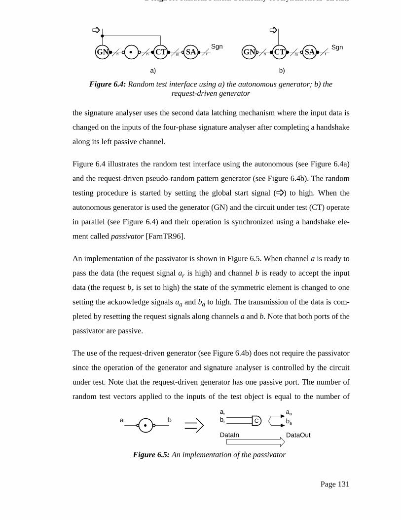
Figure 6.4 illustrates the random test interface using the autonomous (see Figure 6.4a)
and the request-driven pseudo-random pattern generator (see Figure 6.4b). The random
testing procedure is started by setting the global start signal (➩) to high. When the
autonomous generator is used the generator (GN) and the circuit under test (CT) operate
in parallel (see Figure 6.4) and their operation is synchronized using a handshake ele-
ment called passivator [FarnTR96].
An implementation of the passivator is shown in Figure 6.5. When channel a is ready to
pass the data (the request signal ar is high) and channel b is ready to accept the input
data (the request br is set to high) the state of the symmetric element is changed to one
setting the acknowledge signals aa and ba to high. The transmission of the data is com-
pleted by resetting the request signals along channels a and b. Note that both ports of the
passivator are passive.
The use of the request-driven generator (see Figure 6.4b) does not require the passivator
since the operation of the generator and signature analyser is controlled by the circuit
under test. Note that the request-driven generator has one passive port. The number of
random test vectors applied to the inputs of the test object is equal to the number of
mGN CT•n n SA r mGN CTn SA r
➩� ➩�
Figure 6.4: Random test interface using a) the autonomous generator; b) therequest-driven generator
Sgn
a) b)
Sgn
C
Figure 6.5: An implementation of the passivator
ar
br
aa
ba
DataIn DataOut•
a b
Design for Random Pattern Testability of Asynchronous Circuits
Page 132
requests generated on the output channel (Sgn) of the signature analyser. After the
required number of handshakes along channelSgn the signature produced on the output
of the signature analyser is compared with the good one. If they are equal, the circuit is
fault-free, otherwise it is faulty.
As was mentioned in Appendix A an LFSR can be designed to generate all possible
binary vectors on its outputs. Figure A.2b illustrates an implementation of the 4-bit syn-
chronous LFSR which goes through all 16 possible states including the ‘all zeros’ state.
The output sequence of this LFSR has the following unique property:
All possible pairs of 2-bit binary vectors can be found sequentially on the odd or even
outputs of the LFSR [Pet94].
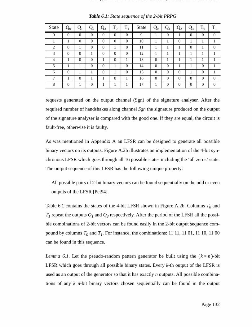
Table 6.1 contains the states of the 4-bit LFSR shown in Figure A.2b. ColumnsT0 and
T1 repeat the outputsQ1 andQ3 respectively. After the period of the LFSR all the possi-
ble combinations of 2-bit vectors can be found easily in the 2-bit output sequence com-
pound by columnsT0 andT1. For instance, the combinations: 11 11, 11 01, 11 10, 11 00
can be found in this sequence.
Lemma 6.1. Let the pseudo-random pattern generator be built using the ()-bit
LFSR which goes through all possible binary states. Everyk-th output of the LFSR is
used as an output of the generator so that it has exactlyn outputs. All possible combina-
tions of anyk n-bit binary vectors chosen sequentially can be found in the output
Table 6.1: State sequence of the 2-bit PRPG
State Q0 Q1 Q2 Q3 T0 T1 State Q0 Q1 Q2 Q3 T0 T1
0 0 0 0 0 0 0 9 1 0 1 0 0 0
1 1 0 0 0 0 0 10 1 1 0 1 1 1
2 0 1 0 0 1 0 11 1 1 1 0 1 0
3 0 0 1 0 0 0 12 1 1 1 1 1 1
4 1 0 0 1 0 1 13 0 1 1 1 1 1
5 1 1 0 0 1 0 14 0 0 1 1 0 1
6 0 1 1 0 1 0 15 0 0 0 1 0 1
7 1 0 1 1 0 1 16 0 0 0 0 0 0
8 0 1 0 1 1 1 17 1 0 0 0 0 0
k n×
Design for Random Pattern Testability of Asynchronous Circuits
Page 133
sequence of the pseudo-random pattern generator after it has passed through all its
states.
1Proof. The prove of this Lemma is trivial fork=1 since the LFSR is assumed to produce
all possible ( )-bit binary vectors on its outputs.
Let us prove this Lemma whenk=2. Hence, the LFSR has 2n outputs.
Let the even outputs of the LFSR be the outputs of the generator. Figure 6.6a shows the
mechanism for generating pseudo-random vectors on the even outputs of the LFSR. Let
us choose a certain pair ofn-bit vectors. The first vector from this pair of vectors is read
directly from the even outputs of the LFSR after the application of a clock signal at time
t (see Figure 6.6). Since the LFSR acts as a shift register the second vector is shifted
from its odd outputs after it is clocked at timet+1. As a result, there is a unique 2n-bit
vector which must be generated by the LFSR in order to produce the required pair of
vectors. Since the LFSR can go through all possible states the required vector can
be derived. This proof can be repeated for any other pairs ofn-bit vectors.
The mechanism for generating pseudo-random vectors on the odd outputs of the LFSR
is illustrated in Figure 6.6b. Let us fix a certain pair ofn-bit vectors. The first vector
from this pair is produced on the odd outputs of the LFSR at timet. After the application
of the next clock the contents of the even flip-flops of the LFSR are shifted into the odd
1. The idea of this proof was suggested by Prof. John Brzozowski in private discussions on thistopic.
k n×
q1(t) q2(t) q3(t) qn(t)
qn(t+1)q3(t+1)q2(t+1)q1(t+1)
1 2 3 4 5 6 2n2n-1
q1(t) q2(t) q3(t) qn(t)
qn(t+1)q3(t+1)q2(t+1)q1(t+1)
1 2 3 4 5 6 2n2n-1
a) b)
Figure 6.6: Mechanisms for generating pseudo-random vectors using a) even andb) odd outputs of the LFSR
2n-2
2n k+
Design for Random Pattern Testability of Asynchronous Circuits
Page 134
ones (see Figure 6.6b) producing the second vector. The content of the first output is
derived by XORing the outputs of some flip-flops including the last one. Note that the
number of inputs of the XOR gate and the flip-flops which feed its inputs depend on the
derivation polynomial of the LFSR. Regardless the outputs of those flip-flops which are
connected to the inputs of the XOR gate the content of the first flip-flop can be inverted
(when the output of the last flip-flop is a one) or can be unchanged (when the output of
the last flip-flop is a zero). As a result, there is a unique state of the LFSR which allows
the required pair of vectors to be generated on its odd outputs.
A similar proof can be continued easily for anyk more than 2. ❑
This property of the LFSR will be used to design of a micropipeline with BIST features
(see section 6.7).
6.2 Sequential circuit designs
The two-phase and four-phase designs of a asynchronous sequential circuit were dis-
cussed in chapter 5. The use of normally closed registersReg1 andReg2 is preferable
for scan testing since the contents of the state registers can be observed and controlled
along a scan path. If the test data is not shifted in and out of the state registers thenReg2
can be transparent initially. As a result, the sequential circuit latch control is faster than
the control of the circuit with normally closed state registers. There is no need to open
the latches ofReg2 every time the data is ready on the outputs of the combinational cir-
cuit. The data from theSO outputs of the combinational circuit is already stored inReg2
when a rising event is generated on theRout output. Note that the latch control of regis-
tersReg1 andReg2 for the two-phase sequential circuit shown in Figure 5.9 assumes
that both the registers are closed initially.
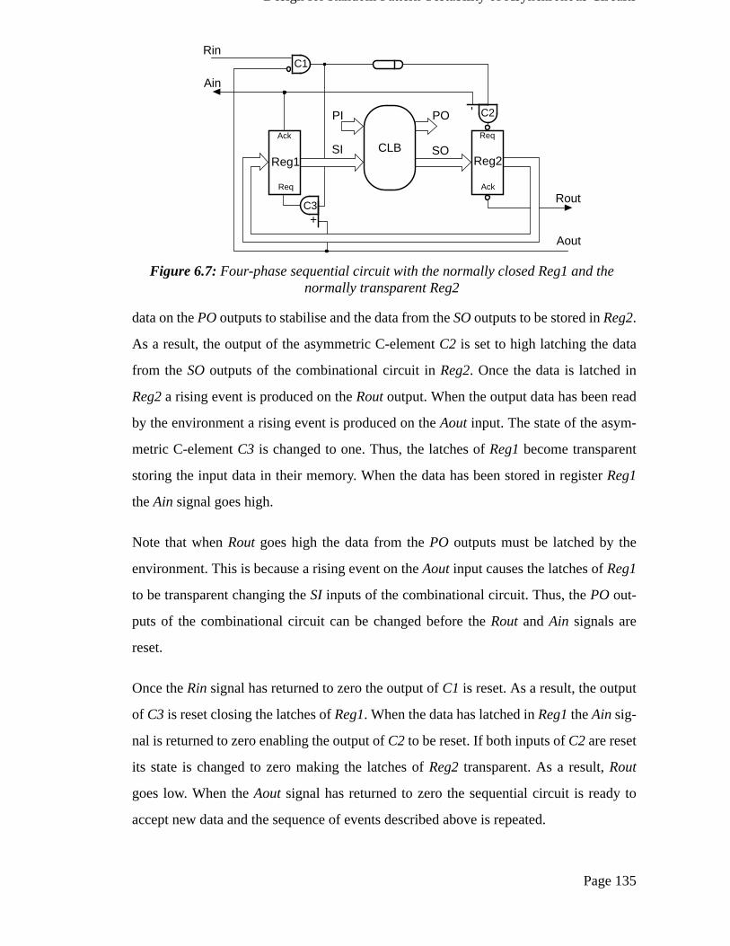
Figure 6.7 shows the design of a four-phase sequential circuit with the normally closed
Reg1 and the normally transparentReg2. Initially, all C-elements are reset. The latches
of Reg1 are set to their initial states. When a rising signal arrives at theRin input the out-
put of the C-elementC1 goes high. This rising signal is delayed for long enough for the
Design for Random Pattern Testability of Asynchronous Circuits
Page 135
data on the PO outputs to stabilise and the data from the SO outputs to be stored in Reg2.
As a result, the output of the asymmetric C-element C2 is set to high latching the data
from the SO outputs of the combinational circuit in Reg2. Once the data is latched in
Reg2 a rising event is produced on the Rout output. When the output data has been read
by the environment a rising event is produced on the Aout input. The state of the asym-
metric C-element C3 is changed to one. Thus, the latches of Reg1 become transparent
storing the input data in their memory. When the data has been stored in register Reg1
the Ain signal goes high.
Note that when Rout goes high the data from the PO outputs must be latched by the
environment. This is because a rising event on the Aout input causes the latches of Reg1
to be transparent changing the SI inputs of the combinational circuit. Thus, the PO out-
puts of the combinational circuit can be changed before the Rout and Ain signals are
reset.
Once the Rin signal has returned to zero the output of C1 is reset. As a result, the output
of C3 is reset closing the latches of Reg1. When the data has latched in Reg1 the Ain sig-
nal is returned to zero enabling the output of C2 to be reset. If both inputs of C2 are reset
its state is changed to zero making the latches of Reg2 transparent. As a result, Rout
goes low. When the Aout signal has returned to zero the sequential circuit is ready to
accept new data and the sequence of events described above is repeated.
Figure 6.7: Four-phase sequential circuit with the normally closed Reg1 and thenormally transparent Reg2
Rin
Rout
Aout
Ain
Reg1
Req
Ack
PI PO
SI SOCLB
C3
C1
+
Ack
Req
Reg2
- C2
Design for Random Pattern Testability of Asynchronous Circuits
Page 136
6.3 Parallel random testing of sequential circuits
6.3.1 Probabilistic properties of an XOR gate
It has already been reported that a 2-input XOR gate can be used to improve the effec-
tiveness of the random testing of synchronous VLSI circuits [Rom89, Souf95].
Consider the XOR gate with two inputs (a and b) and output c shown in Figure 3.2. Let
pa and pb be the probabilities of a one and zero on input a and b respectively. Suppose
that there is no correlation between inputs a and b. Then, according to equation 3.6 the
probability of a one (pc) on output c of the XOR gate can be calculated as follows:
pc = pa + pb - 2papb (6.1)
It is easy to show that if pa=0.5 in equation (6.1) then pc=pa=0.5 regardless of the value
of pb. This probabilistic property of the XOR gate can be described as follows.
If independent and equiprobable random signals are applied to one of the two inputs of
the XOR gate then:
1. The output signals produced by the gate are equiprobable.
2. The probabilistic properties of the output sequence do not depend on the probabilistic
properties of the input sequence applied to the other input.
Clearly, a fault effect can be transmitted easily through the XOR gate since any faulty
signal applied to one of its inputs changes its fault-free output.
6.3.2 Sequential circuit designs for random-pattern testability
The probabilistic properties of the XOR gate can be used for at-speed random testing of
synchronous sequential circuits [Souf95]. In this section asynchronous designs for ran-
dom-pattern testability of sequential circuits are considered.
Design for Random Pattern Testability of Asynchronous Circuits
Page 137
Figures 6.8 and 6.9 show the designs of two-phase and four-phase random pattern testa-
ble sequential circuits. The block of XOR gates performs a bit-wise XOR operation
between theSO outputs of the combinational circuit and additional test inputs (TI). The
outputs of the XOR block are connected to the inputs ofReg2 and test outputs (TO).
During normal operation mode theTI inputs are kept at zero and the sequential circuit
operates according to its specification.
In test mode test vectors generated by the pseudo-random generator are applied to theTI
inputs and thePI inputs. The test results are observed on thePO andTO outputs by the
Figure 6.8: Two-phase sequential circuit with parallel random testing
RinRout
AoutAin
Ack
Req
Reg2Reg1
Req
Ack
PI PO
SISO
C
CLB
C
TI
TO
XOR
Figure 6.9: Four-phase sequential circuit with parallel random testing
Rin
Rout
Aout
Ain
Reg1
Req
Ack
PI PO
SISOCLB
C3
C1
+
Ack
Req
Reg2XOR
TI
TO
- C2
1
2
Design for Random Pattern Testability of Asynchronous Circuits
Page 138
signature analyser. Note that vectors produced by the pseudo-random generator are
equiprobable and independent. Thus, according to the probabilistic properties of the
XOR gate the output vectors produced by the XOR block are equiprobable and inde-
pendent of the probabilistic properties of theSO outputs. As a result, equiprobable and
independent stimuli are applied to the inputs ofReg2 and fault effects from theSO out-
puts can be detected on theTO outputs. After the application of each pseudo-random
test to thePI inputs of the sequential circuit the combinational circuit and registersReg1
and Reg2 are tested concurrently. This random testing procedure is called ‘parallel’
because random test patterns are applied to thePI andSI inputs of the combinational cir-
cuit in parallel.
Stuck-at faults on the inputs and outputs ofReg1 andReg2 are equivalent to the corre-
sponding faults on theSI inputs of the combinational circuit. Stuck-at faults on the
inputs of the XOR block can be easily detected on theTO outputs. As a consequence,
the total test time for detecting stuck-at faults in the data paths of the sequential circuits
(see Figure 6.8 and 6.9) is determined by the random test time of their combinational
circuits.
Number of random patterns required for testing combinational
circuits
There are two important characteristics of random testing:
• the number of patterns which must be produced by the test pattern generator to pro-
duce the desired set of test vectors;
• the probability of detecting all possible faults from the predetermined class of the cir-
cuit’s faults.
The first parameter reflects the practical usability of random testing or simply the ran-
dom pattern testability of the circuit. The second parameter is a characteristic of the
quality of random testing.
Design for Random Pattern Testability of Asynchronous Circuits
Page 139
Suppose that to detect all the stuck-at faults in the predetermined set of the combina-
tional network’s stuck-at faults it is necessary to generate on itsN inputs (N=n+m,
wheren andm are the number ofSI andPI inputs to the combinational circuit respec-
tively) a random test of lengthL.
The test confidence probability threshold () is the probability that all the stuck-at
faults in the circuit will be detected during its random testing. The escape probability
threshold of the test ( ) is the probability that at least one stuck-at fault from
the predetermined set of faults will not be identified.
Thus, the upper bound on the number of random test patterns (L) applied to the inputs of
the combinational circuit can be estimated using the following formula [Savir84,
Wag87]:
, (6.2)
wherepd is the minimal detection probability of a fault from the set of the circuit’s
faults;r is the number of faults which have the minimal detection probabilitypd.
Testing for faults in the control circuits
As was shown in chapters 1 and 5 stuck-at faults on the control lines of the two-phase
sequential circuit illustrated in Figure 6.8 are easy to detect since they cause the circuit
to halt. These faults are detected either in normal operation mode or test mode.
Most stuck-at faults on the control lines in the four-phase sequential circuit shown in
Figure 6.9 violate the communication protocol between the circuit and the environment
causing the circuit to halt. There are some faults which can cause premature firings. For
example, fault 1-SA0 causes a premature falling event on the output ofC2. Fault 2-SA1
causes a premature rising event on the output ofC3.
Fault 1-SA0 cannot be detected by checking the order of events on the control inputs
and the outputs of the circuit. This fault can be detected in test mode by converting the
pt
qt 1 pt–=
Lqt r⁄( )ln
1 pd–( )ln--------------------------≥
Design for Random Pattern Testability of Asynchronous Circuits
Page 140
asymmetric C-element C2 into a symmetric one as shown in Figure 6.10. The symbolic
representation of the C-element C2 and its CMOS implementation are illustrated in Fig-
ure 6.10a and 6.10b respectively. When inputs In1 and In2 are low the p-transistor stack
is on and the output of the C-element is reset. If In1=1 the output of the C-element goes
high. When In1=0 and In2=1 the state of the C-element remains unchanged. Figure
6.10c illustrates a CMOS implementation of the C-element which can operate as a sym-
metric C-element (Tst=0) and the asymmetric one (Tst=1) shown in Figure 6.10b.
After the initialization of all control wires C2 is set to test mode (Tst=0) when it operates
as the symmetric C-element. In the fault-free circuit, when the Rin and Aout inputs are
set to high the Ain and Rout signals go high. In the presence of fault 1-SA0 the output of
C2 cannot be set to high. Thus, the Rout output remains unchanged, i.e. Rout=0. In order
to check if C2 acts as the symmetric or asymmetric C-element the Rin signal must be set
to high after the initialization of the circuit. If Rout goes high C2 operates as the asym-
metric C-element, otherwise it acts as the symmetric one.
Fault 2-SA1 can be detected easily since it violates the order of events on the inputs and
outputs of the circuit. After the initialization the Rin signal is set to high. In the presence
of fault 2-SA1 the output of C3 is set to high. As a result, Ain goes high whereas this
must happen only after setting the Aout input to high.
Out
wkIn1
In2C
In1
In2Out
Figure 6.10: Asymmetric C-element: a) symbol; b) CMOS implementation; c)testable CMOS implementation
a)
c)
-
TstOut
wkIn1
In2
b)
Design for Random Pattern Testability of Asynchronous Circuits
Page 141
6.3.3 Analysis of the parallel random testing technique
Advantages
• The implementation of the parallel random testing technique does not require the
control structure of the sequential circuit to be changed.
• The total test time depends of the random test time of the combinational logic block
and can be calculated easily.
• The sequential circuit is tested at its normal speed which allows a large number of
random test vectors to be applied to the inputs of its combinational circuit.
Disadvantages
• The parallel random testing technique requiresn extra test inputs andn extra test out-
puts, wheren is the number of theSO outputs.
• The technique introduces a certain level of hardware redundancy which includes the
block of two-input XOR gates, the pseudo-random generator and the signature ana-
lyser incorporated into the testable circuit design.
• The block of XOR gates in the feedback of the sequential circuit requires the intro-
duction of an extra delay matching signal delays through the XOR gates.
6.4 Bit-serial random testing of sequential circuits
The general idea for alleviating the test problem of asynchronous sequential circuit
shown in Figures 5.9 and 6.7 is common for all sequential circuits, i.e. during the test the
whole sequential circuit must be divided into a combinational part and memory ele-
ments which are tested separately.
Design for Random Pattern Testability of Asynchronous Circuits
Page 142
6.4.1 Two-phase sequential circuit design
Figure 6.11 illustrates the design of a testable two-phase sequential circuit. This circuit
contains some additional elements such as a register (Reg3) for collecting the test data
from theSO outputs of the combinational circuit, a block of XOR gates to mix the test
data and the multiplexer to switch the data flow during the test phase. Also there are two
XOR gates, multiplexers and a toggle element to provide the proper control signalling.
C
C
Figure 6.11: Two-phase sequential circuit with bit-serial random testing
Rin
Ain
Aout
Rout
MX
MX
MX
XOR
delay1
Togg
le
dela
y2
PI
PO
n
n-1
n
n
n
Sin
Sout
n
n
n
TF
F
T
F
T
OM
OM
SI
SO
CLB
Reg3 ReqAck
Reg2Req Ack
Reg1Req Ack
Design for Random Pattern Testability of Asynchronous Circuits
Page 143
The sequential circuit performs in two modes (normal operation and test mode) which
are set by switching the Boolean signal on the operation mode input (OM). There are
two additional pins (Sin andSout) inserted in the design to scan test patterns intoReg1
for stimulating theSI inputs of the combinational circuit and scan its responses out dur-
ing the test.
Test mode
In test mode, the Boolean signalOM is set to high. The control part of the circuit shown
in Figure 6.11 is reconfigured to provide the desired asynchronous test control interface.
All the latches ofReg1 are set to their initial states whereas all the latches ofReg3, all
the C-elements and the toggle element are set to zero. The primary inputs (PI) of the
combinational circuit and theSin input of the circuit are connected to the outputs of the
two-phase pseudo-random generator. The responses from thePO outputs of the combi-
national circuit and theSout output of the sequential circuit are compressed by the two-
phase signature analyser.
A request signal (Rin) from the generator is delayed for long enough for the output data
to stabilize on the outputs of the combinational logic block. The data from theSO out-
puts of the combinational circuit is mixed with the output data ofReg3 in the block of
two-input XOR gates. The outputs of the XOR gates come through the multiplexer to
the inputs ofReg2 and are latched inReg2. After receiving an acknowledge signal from
Reg2, which is steered by the toggle element, the content ofReg2 is copied intoReg3.
When the data is captured byReg3 it generates an acknowledge signal on its outputAck.
This signal causes the multiplexer to connect the first (n-1) most significant bits ofReg1
and the scan-in inputSin of the circuit to the inputs ofReg2. Simultaneously, a request
signal is produced for the signature analyser on theRout output. The data from the out-
puts of the multiplexer is captured byReg2 when a new request signal appears on its
request inputReq (in fact, this is the acknowledge signal forReg3 which is delayed until
the multiplexer has switched). A new acknowledge signal fromReg2 is steered by the
toggle element and passes to the corresponding input of the symmetric C-element where
Design for Random Pattern Testability of Asynchronous Circuits
Page 144
it waits for an acknowledge signal from the signature analyser. The primary outputs of
the combinational circuit and the scan-out output ofReg3, which is actually thenth bit
of Reg3, are collected by the signature analyser. Once an acknowledge signal is received
on theAout input:
1) the content ofReg2 is copied intoReg1;
2) an acknowledge signal is sent to the generator.
When the generator has finished producing a new test pattern, a new request signal is
generated on theRin input of the circuit and the test procedure described above is
repeated again.
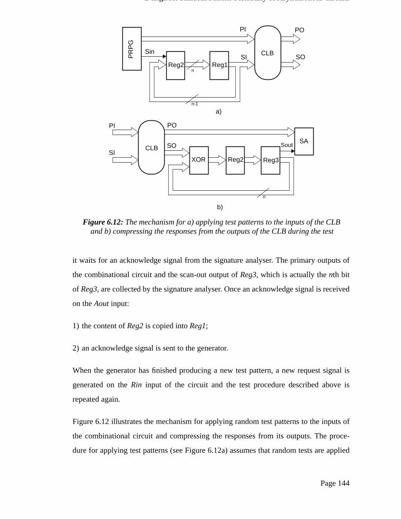
Figure 6.12 illustrates the mechanism for applying random test patterns to the inputs of
the combinational circuit and compressing the responses from its outputs. The proce-
dure for applying test patterns (see Figure 6.12a) assumes that random tests are applied
CLBPR
PG
Reg1n
n-1
Sin
PI PO
SI SO
Reg2XOR Reg3
SACLB
PO
SOSI
PI
n
Sout
Figure 6.12: The mechanism for a) applying test patterns to the inputs of the CLBand b) compressing the responses from the outputs of the CLB during the test
a)
b)
Reg2
Design for Random Pattern Testability of Asynchronous Circuits
Page 145
both to thePI inputs of the combinational circuit and theSin input of the sequential cir-
cuit. During the test registersReg1 andReg2 are configured to shift a new test bit to
Reg1 after receiving a request signal from the generator. As a result, random test bits are
shifted inReg1 bit-serially from theSin input of the circuit.
The process of collecting and compressing test data from the outputs of the combina-
tional circuit (see Figure 6.12b) consists of two parts. The first one includes the direct
analysis of the responses from thePO outputs of combinational circuit by means of the
external signature analyser. The second part is a signature analyser which compresses
the responses from theSO outputs of the combinational circuit. RegistersReg2, Reg3
and the block of XOR gates are configured in such way that the current contents ofReg3
are mixed (with the help of the XOR operation) with a new response which is produced
on theSO outputs of the combinational circuit. The contents ofReg3 are observed on its
n-th output.
SO15 SO14 SO0
L215
L2L2L314 0L3 L3
01415
Sout
L2 L3
L2 L3 L2 L3
L2 L3 L2 L3 L2 L3
SO15 r( )
SO14 r( )
SO0 r( )
SO1 r( )Sout(r)
1 2 15
Figure 6.13: Compressing the test data from the internal outputs of the CLB: a) thestructure of the signature analyser; b) the equivalent schematic of the signature
analyser
a)
b)
L2L3
Design for Random Pattern Testability of Asynchronous Circuits
Page 146
The signature analyser used for collecting the test data from the SO outputs of the com-
binational circuit is illustrated in Figure 6.13. The general structure of this signature
analyser (see Figure 6.13a) is similar to the structure of the BILBO signature analyser
(see Appendix B). The equivalent schematic of such a signature analyser (see Figure
6.13b) shows that the procedure for compressing the test data from the SO outputs of the
combinational circuit is similar to the XOR operation. After receiving each request sig-
nal (r) the input bits are delayed for a different number of steps (request signals) depend-
ing on their position numbers and then XORed.
Normal operation mode
In normal operation mode, the OM input of the sequential circuit is reset. The outputs of
the toggle element and the outputs of Reg3 are held at zero permanently. Initially, all the
C-elements are reset. The latches of Reg1 are set to their initial states. After receiving a
request signal at the Rin input from the sender data is processed by the sequential circuit
in the same way as was described for the circuit shown in Figure 5.9.
6.4.2 Four-phase sequential circuit design
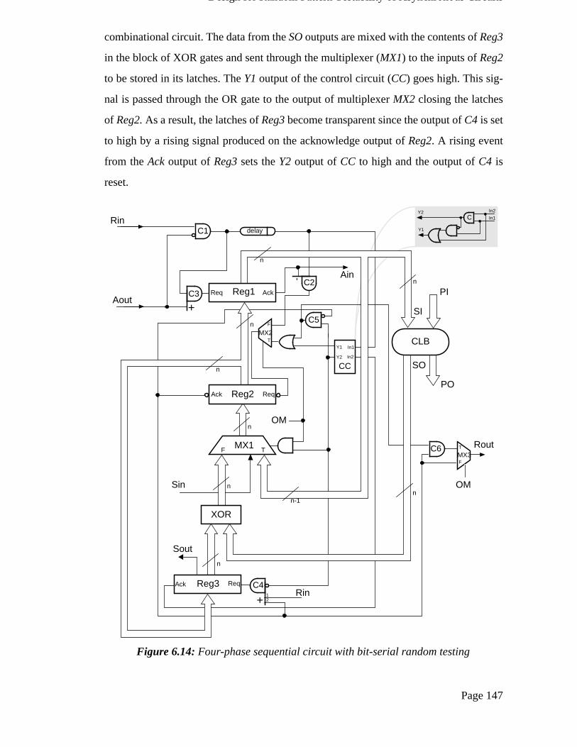
Figure 6.14 shows the design of a four-phase sequential circuit with bit-serial random
testing. This circuit performs in two modes depending on the value applied to the
Boolean signal OM: test (OM=1) and normal operation mode (OM=0).
Test mode
In test mode the OM input is set to high and all C-elements are reset. The latches of
Reg1 are set to their initial states. The latches of Reg3 are reset. Note that registers Reg1
and Reg3 are closed whereas the latches of Reg2 are transparent initially.
When a test vector has been applied to the PI and Sin inputs by the four-phase pseudo-
random generator the Rin signal goes high setting the output of C1 to high. This signal is
delayed for long enough for the output data to stabilize on the PO and SO outputs of the
Design for Random Pattern Testability of Asynchronous Circuits
Page 147
combinational circuit. The data from the SO outputs are mixed with the contents of Reg3
in the block of XOR gates and sent through the multiplexer (MX1) to the inputs of Reg2
to be stored in its latches. The Y1 output of the control circuit (CC) goes high. This sig-
nal is passed through the OR gate to the output of multiplexer MX2 closing the latches
of Reg2. As a result, the latches of Reg3 become transparent since the output of C4 is set
to high by a rising signal produced on the acknowledge output of Reg2. A rising event
from the Ack output of Reg3 sets the Y2 output of CC to high and the output of C4 is
reset.
Figure 6.14: Four-phase sequential circuit with bit-serial random testing
Rin
Aout
RoutMX1
MX2
XOR
delay
PI
PO
n
n-1
n
n
n
Sin
Sout
n
n
TF
T
F
OM
OM
SI
SO
CLB
Reg3 ReqAck
Reg2Ack Req
Reg1Req Ack
C4
+
C6
C1
MX3F
T
C3
+
nC5
n
- C2Ain
12
CC
In1
In2
Y1
Y2
CIn2
In1
Y1
Y2
Rin
Design for Random Pattern Testability of Asynchronous Circuits
Page 148
The latches ofReg3 become opaque storing in their memory a current signature of the
data produced on theSO outputs of the combinational circuit. The mechanism for col-
lecting the data form theSO outputs was discussed in the previous section of this chap-
ter.
Note that a high signal from theY2 output ofCC switches multiplexerMX1 so that it
connects the (n-1) less significant outputs ofReg1 and theSin input to the inputs of
Reg2. A falling signal from theAck output ofReg3 resets theY1 output ofCC making
the latches ofReg2 transparent. Afterwards a falling signal from theAck output ofReg2
sets the output ofC5 to high. As a consequence, the latches ofReg2 become opaque
again. Once theAck output ofReg2 is set to high the state ofC6 is changed to one pro-
ducing a rising event on theRout output of multiplexerMX3.
When the data form thePO outputs and theSout output has been collected by the exter-
nal signature analyser theAout signal goes high. The output ofC3 is set to high making
the latches ofReg1 transparent. A rising signal from theAck output ofReg1 is passed to
theAin output of the circuit. Once theRin signal is returned to zero the output ofC1 is
reset changing the state ofC3 to zero. As a result,Reg1 is closed storing a new test vec-
tor which is applied to theSI inputs of the combinational circuit. The mechanism for
producing tests for theSI inputs of the combinational circuit is similar to that described
in the previous section of this chapter.
The Y2 output ofCC is reset changing the state ofC5 to zero. The latches ofReg2
become transparent and a falling event is generated on theAck output ofReg2. Thus,C6
moves to the zero state resetting theRout output of the circuit. If theAout input is reset
the sequential circuit is ready to accept a new test from the generator and the sequence
of events described above is repeated.
Normal operation mode
When the Boolean signalOM is low the sequential circuit performs in normal operation
mode. In the initial state all the C-elements are reset. The latches ofReg1 are set to their
Design for Random Pattern Testability of Asynchronous Circuits
Page 149
initial states. The output of the symmetric C-element of CC is kept high (see Figure
6.14) and the outputs of Reg3 are kept low during normal operation mode. When the
data is ready on the PI inputs and the Rin input is set to high the sequential circuit oper-
ates in the same manner as the circuit shown in Figure 6.7.
6.4.3 Analysis of the bit-serial random test technique
Advantages
The random pattern testable sequential circuits shown in Figures 6.11 and 6.14 have
some important features which simplify their random testing.
Complexity of the test procedure. During the test the combinational part of the sequen-
tial circuit is tested separately from the memory elements which makes the testing of the
circuit much easier.
Test performance. Compared to the scan test approach the bit-serial test procedure does
not require a test pattern to be scanned into the shift register before the testing and the
test data to be scanned out after the application of the test pattern. During the random
testing of the sequential circuits (see Figures 6.11 and 6.14), test patterns are produced
on the SI inputs of their combinational circuits with the help of shifting the contents of
Reg1 by one bit. A new test bit is loaded from the generator after receiving a request sig-
nal. The test data from the SO outputs of the combinational circuit is collected in Reg3
after the application of each new test pattern to the inputs of the combinational circuit.
There is no need to shift all the contents out of Reg3 after applying a new test pattern to
the inputs of the circuit (the test data is compressed and stored into register Reg3 and
observed on its n-th output after the application of each test pattern). In this case the ran-
dom pattern testing of such a circuit is approximately (n-1) times faster then a traditional
scan test method, where n is the number of latches of Reg1.
Number of random test patterns. The analysis of the circuits illustrated in Figures 6.11
and 6.14 shows that the number of random test patterns required to detect all their single
Design for Random Pattern Testability of Asynchronous Circuits
Page 150
stuck-at faults in the data paths is equal to the number of test patterns for detecting all
the stuck-at faults in their combinational parts. This is because of the following proper-
ties:
• all the stuck-at faults on the inputs/outputs of registersReg1 andReg2 are equivalent
to the corresponding faults on theSI inputs of the combinational logic block;
• all the stuck-at faults on the inputs/outputs of the block of XOR gates andReg3 are
detected easily during the test of the combinational circuit (the circuitry which col-
lects the test data from the internal outputs of the combinational circuit (see Figure
6.13) is similar to the BILBO register);
The use of either equiprobable or weighted random test patterns. The bit-serial random
testing allows either equiprobable or weighted random test vectors to be applied to the
inputs of the combinational circuit during its testing.
Random testing using only equiprobable random test patterns is not always the optimal
test procedure for obtaining the minimal (or close to minimal) number of random test
patterns in order to guarantee the detection of all the circuit’s stuck-at faults. In order to
reduce the number of random test patterns, special methods have been derived for
achieving optimal output signal probabilities for generators of weighted pseudo-random
test patterns [Agra76, ChinTR84, Waic89]. The upper bound for the random test length
L can be calculated using formula (6.2).
Disadvantages
Complex circuit control. Two-phase and four-phase implementations of the bit-serial
random testing technique require the initial control circuit of the corresponding sequen-
tial circuit to be changed. The introduction of extra elements into the control circuit can
make its testing more difficult.
A fault simulation analysis of the two-phase and four-phase control circuits was carried
out usingSIMIC design verification tools [Sim94]. It was observed that stuck-at faults
Design for Random Pattern Testability of Asynchronous Circuits
Page 151
on the control lines of the two-phase sequential circuit (see Figure 6.11) are easy to
detect since either they cause the circuit to halt or they change the data flow during the
test which can be identified easily. There are some stuck-at faults in the two-phase con-
trol circuit (on the false inputs of the control multiplexers) which cannot be detected in
test mode. They will manifest themselves during normal operation mode by preventing
any activity on theRout andAin outputs, hence causing the whole circuit to deadlock.
In the four-phase sequential circuit shown in Figure 6.14 most stuck-at faults on the con-
trol lines manifest themselves during the test by causing the circuit to halt. A stuck-at
fault on the control input ofMX1 can be detected easily since it changes the data flow
during the test. Note that stuck-at faults on the control wires which are not involved in
test mode can only be identified during normal operation mode by causing the circuit to
halt.
The stuck-at faults which cause premature firings on the outputs ofC2 andC3 can be
tested in the same manner described in section 6.3.2. Faults 1-SA1 and 2-SA1 cause pre-
mature rising events on the output ofC4. These faults can be detected by converting the
asymmetric C-element into a symmetric one using an additional control input (Tst) as
shown in Figure 5.13. After the initialization the following sequence of steps can be
used to identify these faults:
1. OM=1.
2. Tst is set to high. C4 operates as a symmetric C-element.
3. Rin↑
TheAck output ofReg2 goes high setting the output ofC4 to high. As a result, theY2
output ofCC goes high.
3. Aout↑ andRin↓
The output ofC2 is reset.
Design for Random Pattern Testability of Asynchronous Circuits
Page 152
4. When the Ain output has reset OM=0.
The Multiplexer MX2 is switched connecting the output of C2 to the Req input of
Reg2. Thus, C4 goes to the zero state if it is fault-free and the output of C4 remains
unchanged in the presence of faults 1-SA1 and 2-SA1. Note that the output of C5 is
set to high.
5. OM=1.
Fault-free behaviour. The outputs of CC are reset. The Ack output of Reg2 goes high
changing the state of C6 to one. Afterwards, the output of C5 is reset and the output
of C6 is set to low. As a result, the Rout output goes high and then low.
Faulty behaviour. The outputs of CC remain unchanged (Y1=Y2=1). The output of
C6 is set to high and the Rout signal goes high.
The operation mode of the C-element C4 (symmetric or asymmetric) can be checked by
setting the sequential circuit in test mode and applying the sequence of events described
in section 6.4.2. If C4 operates as the symmetric C-element the whole circuit will halt.
Hardware redundancy. The hardware redundancy of the testable sequential circuits con-
sists of register Reg3, the block of n XOR gates, three multiplexers, the toggle element
and extra control elements to provide for the corresponding signalling. Clearly, the over-
all hardware redundancy of the testable circuit heavily depends on the complexity of its
combinational logic block: the more complex the combinational circuit is, the less
redundancy the testable sequential circuit has. As a result, this method of designing test-
able asynchronous sequential circuits is more effective in terms of hardware redundancy
for complex sequential circuits.
Performance degradation. There is some degradation in the performance of the testable
sequential circuits during normal operation mode. This is caused by the additional cir-
cuits incorporated in the data paths and the control circuit which inevitably slows down
the circuit performance.
Design for Random Pattern Testability of Asynchronous Circuits
Page 153
6.5 Handshake implementations of a sequential circuit forrandom pattern testability
6.5.1 The design of a handshake sequential circuit
A sequential circuit can be implemented as the handshake circuit shown in Figure 6.15.
This circuit has one input communication channel (pi) along whichm-bit input data is
sent and one output channel (po) from whichk-bit output data is read by the environ-
ment. The sequential circuit comprises two storage elements (R1 andR2) to store the
states of the circuit and the combinational block (CL) which performs the logic function
producing the outputs and new states for the sequential circuit.
Initially, theR2 storage element is reset into its initial state according to the specification
of the sequential circuit. The handshake circuit is activated along its activation channel
(➩�). As a result, the contents of theR2 storage element is copied intoR1. Afterwards,
the passive port of the combine element (<<>>) is triggered by the corresponding
sequencer.
;
T
R1
*➩�
R2
T
;*
*
Figure 6.15: Handshake implementation of a sequential circuit
<<>>
TCL
T
m
k
n
n
popi
Design for Random Pattern Testability of Asynchronous Circuits
Page 154
An implementation of the combine element is shown in Figure 6.16a [FarnTR96]. The
combine element is activated along its channel a which is the passive channel of the fork
(the design of the fork is illustrated in Figure 6.16b). The fork passes a request signal
from channel a to the request outputs of channel a and b in parallel. When the data has
ready on the data inputs of channels b and c rising acknowledge signals are sent to the
fork setting the output of the symmetric C-element to high (see Figure 6.16b). When the
data has been read from the data outputs of the combine element the request wire of
channel a is returned to zero resetting the corresponding request wires of channels b and
c. A handshake along input and output channels of the combine element is completed
when the acknowledge signals of channels b and c are returned to zero.
The combine element reads the data from the outputs of R1 and inputs of the pi channel.
The transferer sends the data from the outputs of the combine element to the inputs of
the combinational circuit. A handshake implementation of the combinational circuit is
illustrated in Figure 6.16c. When the data has arrived at the inputs of the combinational
circuit ar goes high. This signal is delayed for long enough for the output data to stabi-
lize on the outputs b and c. Note that the outputs b and c of the combinational circuit
correspond to the primary and state outputs of the circuit respectively. A handshake
along the input channel is completed when the ar and aa signals are returned to zero.
The output data produced by the combinational circuit is read by activating the corre-
sponding output channels.
When the data is ready to be read from the outputs of the combinational circuit the top
sequencer triggers the fork which activates the corresponding transferers (see Figure
6.15). The data from the primary and the state outputs of the combinational circuit is
transmitted in parallel to the po channel and the R2 storage element respectively. When
the output data is stored in R2 and read by the environment the contents of R2 is copied
to R1. As a result, the sequential circuit generates a request for new data to be sent to its
pi channel.
Design for Random Pattern Testability of Asynchronous Circuits
Page 155
Figure 6.16: Handshake implementations of the a) combine element; b) fork; c)combinational circuit; d) bitwise XOR operation; e) case element; f) mixer; g)
multiplexer
<<>>
a[n+m-1:0]
b[m-1:0]
c[n-1:0]
c
b
a
ar
aa
ba
br
ca
crCLBa[n+m-1:0]
b[k-1:0]
c[n-1:0]
CLa
b
c
c
b
a
a) b)
C
ar
br
cr
ba
caaa
a
b
c
XOR
a
c
b
c[n-1:0]
b[n-1:0]a[n-1:0]
a
c
b
d)c)
CCaa
ar
ca cr
|a
b
c@
aaba
ca
ar
Sel
ect 1
0
br
cr
a
b
cOM
OM
CC
|
R
S Q
ar
ca
cr
aa ba
selbr
nQ
a[n-1:0]
b[n-1:0] MX
0
1
c[n-1:0]a
b
c
br
ba
f)e)
g)
Design for Random Pattern Testability of Asynchronous Circuits
Page 156
Figure 6.17 shows an example of the Tangram procedureSC performed by the sequen-
tial circuit illustrated in Figure 6.15. According to this procedure the input data is
assumed to be stored by the environment in a variable calledinput. Initially, the variable
r2 is reset by theResetState procedure. Afterwards, the set of commands written
between theforever do andod lines is performed infinitely. Thus, the contents of varia-
bler2 is copied intor1 and new data is read frominput along thepi channel. A new state
vector produced by functionCombFunction1 is written inr2 and the output data pro-
duced by functionCombFunction2 is transmitted from the primary outputs of the com-
binational circuit to thepo channel concurrently. Note that the function of the
combinational circuit shown in Figure 6.16c is the union of combinational functions
CombFunction1 andCombFunction2.
Fault model
In this section two single stuck-at fault models are considered in the design of the hand-
shake sequential circuit:
• the stuck-at output faults on the control lines of its handshake components;
• the stuck-at input and output faults in the circuit data paths.
Figure 6.21: Bit-serial random testing procedure SC_BST
Design for Random Pattern Testability of Asynchronous Circuits
Page 163
Normal operation mode
The BooleanOM is reset in normal operation mode allowing the lower active channel of
the case element to be controlled from its passive channel. The outputs of the storage
elementR3 are held at zero permanently. As result, the handshake sequential circuit
shown in Figure 6.20 performs in the same manner as the one described in Figure 6.15.
6.6 A case study of the AMULET2e memory controller
An extended version of the AMULET2 microprocessor called AMULET2e has been
implemented to connect the microprocessor to a wide variety of static and dynamic
memories and peripheral chips. Figure 6.22 shows a block diagram of the AMULET2e
microprocessor which incorporates the AMULET2 processor core together with an on-
chip cache and an external memory interface.
The memory interface of the AMULET2e microprocessor includes a memory controller.
The memory controller is a finite state machine which has seven inputs (m=7), four out-
puts (k=4) and 3-bit coded states (n=3). The state table for the AMULET2e memory
controller is shown in Table D.1 in Appendix D.
Two-phase, four-phase and handshake designs of the memory controller have been
implemented in CMOS technology on a 1 double layer metal process and simulated
Figure 6.22: Block diagram of the AMULET2e microprocessor
Cache
memory
Memoryinterface
x[6:0]
f[3:0]
Memorycontroller
AMULET2
processor
core
Address
Data
adr[29:0]
data[31:0]
ms[7:0]
wr[3:0]
cas[3:0]
read
treq
tack
Reset
µm
Design for Random Pattern Testability of Asynchronous Circuits
Page 164
using SIMIC design verification tools. Simulation results of the three versions of the
memory controller, i.e. the controller without testability features, with bit-serial and par-
allel random testing, implemented as two-phase, four-phase and handshake sequential
circuits can be found in Tables 6.2, 6.3 and 6.4 respectively. The notation used in these
tables is as follows:
PD is the performance degradation, AO is the area overhead, NM and TM is normal
operation mode and test mode respectively.
Table 6.2: Two-phase implementations of the AMULET2e memory controller
DesignPerformance,
ns/testPD,%
Area, AO,%
Powerconsumption,
nJ/testNM TM NM TM
Without testability 16.8 n/a n/a 10.6 n/a 48.1 n/a
Bit-serial 18.8 33.5 12% 13.4 26% 54.2 73.1
Parallel 17.9 17.9 7% 10.9 3% 50.3 59.4
Table 6.3: Four-phase implementations of the AMULET2e memory controller
DesignPerformance,
ns/testPD,%
Area, AO,%
Powerconsumption,
nJ/testNM TM NM TM
Without testability 14.7 n/a n/a 9.9 n/a 50.6 n/a
Bit-serial 17.1 30.4 15% 12.1 22% 63.8 88.2
Parallel 15.6 15.6 6% 10.2 3% 52.9 60.2
Table 6.4: Handshake implementations of the AMULET2e memory controller
DesignPerformance,
ns/testPD,%
Area, AO,%
Powerconsumption,
nJ/testNM TM NM TM
Without testability 18.1 n/a n/a 10.0 n/a 53.9 n/a
Bit-serial 22.5 38.7 24% 12.9 29% 69.0 94.2
Parallel 19.3 19.3 7% 10.3 3% 56.5 64.2
102–× mm
2
102–× mm
2
102–× mm
2
Design for Random Pattern Testability of Asynchronous Circuits
Page 165
Comparing different implementations of the memory controller the bit-serial DFT
implementations exhibit the highest performance degradation in normal operation mode
which varies from 12% for the two-phase design to 24% for the handshake implementa-
tion. This is because the control circuits used in the bit-serial DFT designs of the mem-
ory controller have to be changed by adding extra control elements which slow them
down. As a result, the bit-serial DFT designs consume more switching energy demon-
strating the largest power consumption.
The parallel DFT designs of the memory controller have the minimal area overhead
(3%) contributed by the block of three XOR gates. Note that the data for the parallel
DFT designs does not include the area overhead of the internal pseudo-random genera-
tor and signature analyser together with extra test wires required for stimulating the
inputs of the XOR gates and observing the test results from the their outputs. Thus, the
total area overhead of the parallel DFT designs can be much larger.
Figure 6.23: Graph dependencies between the percentage of detected faults and thenumber of random tests applied to the inputs of the memory controller without
testability features (graph 1) and the one designed for testability (graph 2)
1.0 1.5 2.0 2.5 3.0 3.560
70
80
90
100%
log10L
2
1
Design for Random Pattern Testability of Asynchronous Circuits
Page 166
It can be seen from Tables 6.2, 6.3 and 6.4 the designs of the memory controller with
testability features dissipate more energy than the implementations without testability
(see chapter 3).
Finally, the four-phase designs of the memory controller exhibit the best performance in
both test and normal operation modes whereas the implementations of the two-phase
designs exhibit the lowest performance degradation.
Figure 6.23 shows graphs 1 and 2 which demonstrate the dependencies between the per-
centage of detected faults in the combinational circuit of the memory controller and the
number of random test patterns applied to the inputs of the controller without testability
features and its parallel and bit-serial DFT designs respectively. The fault simulation
analysis was carried out with the help ofSIMIC design verification tools. Note that the
number of tests in Figure 6.23 is represented in a logarithmical scale on the base 10. As
follows from Figure 6.23 the percentage of detected faults in the memory controller and,
hence, its random pattern testability is higher in the second case (graph 1 lies below
graph 2).
In order to calculate the number of equiprobable random tests required for testing the
combinational circuit of the memory controller formula (6.2) can be used. A fault simu-
lation analysis carried out with the help of theSIMIC fault simulator showed that there
are 8 stuck-at faults (r=8) in the combinational part of the controller which have the
minimal detection probability (pd= ). As a result, the upper bound of the ran-
dom pattern test length is equal toL=2243 andL=3422 forpt=0.9 andpt=0.99 respec-
tively. According to Figure 6.23 all the stuck-at faults in the combinational circuit of the
controller are detected after the application of 2000 random tests and 1000 random tests
for case 1 and 2 respectively.
1.95 103–×
Design for Random Pattern Testability of Asynchronous Circuits
Page 167
6.7 Built-in self-testing of micropipelines
In this section the BIST design of a micropipeline based on the BILBO technique (see
Appendix B) is considered.
6.7.1 Asynchronous BILBO register design
The CMOS implementation of one of the latches from which an asynchronous BILBO
register is built is illustrated in Figure 6.24. The latch design consists of two latches L1
and L2 connected together. The implementation of L1 is similar to the single-phase static
latch shown in Figure 5.3. In addition, latch L1 has an active low set input to set the
Dout1 output to high. Latch L2 is a single-phase static latch which is transparent when
its enable input is low otherwise it is opaque. L2 has an active low reset input which
holds its output at zero regardless of whether it is transparent or opaque.
Initially latch L1 is closed and L2 is opened by a low signal applied to its En input. When
the data is stable on the Din input of L1 the En input is set to high making the latch L1
transparent and L2 opaque. The input data stored in the memory of L1 is passed to the
Figure 6.24: CMOS implementation of the BILBO register latch
L1
L2
Reset
En
Din
Dout1
Dout2
Set
wk
wk
wk
wk
Design for Random Pattern Testability of Asynchronous Circuits
Page 168
Dout1 output and to the data input ofL2. When the enable input is reset latchL1 is closed
andL2 is transparent storing the data fromL1 in its memory. As a result, the data stored
in L1 is passed to theDout2 output of the register latch. The procedure of storing data in
the register latch is similar to that of a master-slave flip-flop. Note that whenEn=0 the
Dout1 output can be set to high by an active low signal applied to theset input ofL1.
An asynchronous implementation of a 4-bit BILBO register is illustrated in Figure 6.25.
TheQi outputs of theLi1 latches (i=0,1,2,3) are used as the outputs of the BILBO regis-
ter. TheDout2 outputs of the register latches (see Figure 6.24) are connected through the
XOR gates to theDin inputs of the corresponding latches. Thescan-in input (Sin) is
coupled through the multiplexer (MX) and one of the inputs of the XOR gate to theDin
input of the first register latch. TheDout2 output of the last register latch is used as a
scan output of the register. The register latches can be enabled byscan anddata enable
clocks applied to theSc input of the register and theDe input of the OR gate respec-
tively. TheDe clocks are generated by the latch control circuit which can operate using
either two-phase or four phase signalling (see chapter 5).
Figure 6.25: Asynchronous BILBO register structure
Sout
Sc
Sin
C1
C2
Ain AoutRin De
En
MXF
T
Set
L01
L02
L11
L12
L21
L22
L31
L32
In0
Q0 Q1
In1 In2 In3
Reset
Rout
Latch Control
Q2 Q3
Design for Random Pattern Testability of Asynchronous Circuits
Page 169
The BILBO register shown in Figure 6.25 can act in four distinct operation modes
depending on the control signalsC1 andC2: normal, shift, LFSR and signature analyser
operation modes. Table 6.5 contains the values for the control signals and the corre-
spond operation modes of the BILBO register.
Normal operation mode. In this modeC1=1 andC2=0. As a result, thereset signal is set
to low holding the outputs of latchesLi2 (i=0,1,2,3) at zero permanently. Theset input is
high. The inputsSin andSc are kept low during this operation mode.
When the input data is stable on theIn inputs of the register the control inputs of the
latch control block are activated by the environment. Thus, clock signals are produced
on theDe output by the latch control circuit. The data is passed to the outputs of theLi1
latches and latched in their memories.
Shift register mode. Control signalsC1 andC2 are reset in the shift register operation
mode of the BILBO register. In this mode theset andreset signals are set to high. The
register latches act as D-type flip-flops configured in a 4-bit shift register. The shift reg-
ister is clocked from theSc input. Note the latch control block is not active in this mode
holding itsDe output at zero permanently.
When the scan data is ready on theSin input it is transmitted through the multiplexer to
the input of the first flip-flop. A clock signal is applied to theSc input of the register. As
a result, the scan data is stored in the first flip-flop and passed to the input of the second
flip-flop. The next bits of the scan data is shifted into the register latches in the same
manner as a normal shift register operates. The shift register passes the scan data on its
Sout output from where the data is read by the environment.
Table 6.5: Operation modes of the BILBO register in Figure 6.25
C1 C2 Set Reset Mode1 0 1 0 Normal
0 0 1 1 Shift
0 1 0→1 1 LFSR
1 1 0→1 1 SA
Design for Random Pattern Testability of Asynchronous Circuits
Page 170
LFSR operation mode. The BILBO register operates as an LFSR whenC1=0 andC2=1.
In this mode, thereset signal is set to high and theSc input is reset. Note that the data
from theIn inputs of the BILBO register is blocked by a zero signal applied to itsC1
input (the outputs of the corresponding AND gates are reset). Thus, the BILBO register
(see Figure 6.25) can perform as the 4-bit LFSR illustrated in Figure A.2a.
Initially, the set input of the register is reset setting theQi outputs and the outputs of
latchesLi2 (i=0,1,2,3) to high. When the register outputs are stable theset input is set to
high. As a result, the ‘all ones’ state is the initial state of the LFSR. The LFSR generates
a new output vector every time when a new clock signal is produced by the latch control
block on itsDe output.
Signature analyser operation mode. When the control signalsC1 andC2 are set to high
the BILBO register can operate as a signature analyser. In this mode, thereset signal is
set to high and theSc input is reset permanently. Note that the data from theIn inputs of
the register is enabled by a high signal applied to theC1 input. As a result, the BILBO
register is configured as the 4-bit signature analyser shown in Figure A.4.
In the initial state the outputs of the signature analyser are set to high by a low signal
applied to theset input of the BILBO register. When the outputs of the signature ana-
lyser are stable the set signal is set to high. Once the data are ready on theIn inputs the
signature analyser is clocked from theDe output of the latch control block. As a result,
the current contents of the register is mixed with the new input data in the same manner
described in Appendix A.
The design of the asynchronous BILBO register shown in Figure 6.25 is similar to the
one considered in Appendix B. As a consequence, the testability properties of the asyn-
chronous BILBO register towards its stuck-at faults is the same as that of the synchro-
nous one. Note that all stuck-at faults of the BILBO register including faults on either
the control lines or its data paths can be detected when the register is forced to perform
in all its operation modes.
Design for Random Pattern Testability of Asynchronous Circuits
Page 171
6.7.2 Micropipeline structure with BIST features
Figure 6.26 shows a two-stage micropipeline structure with BIST features. The stage
registers of this micropipeline are built from the asynchronous BILBO register illus-
trated in Figure 6.25. The outputs of the micropipeline can be connected to its inputs
depending the Boolean Bist which is high in BIST mode and low in normal operation
mode. The BIST control unit is activated by a high signal applied to the Bist input of the
micropipeline allowing the BIST control signals to be generated. The RSin, ASin, RSout
and ASout control signals are used in an asynchronous interface to shift the data in and
out of the stage registers. These signals have the same meaning as the ones described in
chapter 5.
Normal operation mode
The micropipeline is set to normal operation mode when Bist=0 and RSin= ASout=0. As
a result, the control signals Ci1 and Ci2 (i=1,2) of the control unit are set to high and low
respectively. Its Set and Sc outputs are set high and low respectively. In this mode the
micropipeline acts in the same manner described in chapter 1, section 1.4.
Figure 6.26: A two-stage micropipeline with BIST features
Din
Rin
AinSin Sout
Rout
Aout
Dout
SoutSin
Reg2
Sc
C1
C2
BIST Control Unit
RSin
ASin ASout
RSout
Rin Rout
Ain Aout
SoutSin
Reg1
Sc
C1C2
Rin Rout
Ain AoutSet Set
CL1MX
F
T
Bist
C11 C12 C21 C22 Set Sc
CL2
Design for Random Pattern Testability of Asynchronous Circuits
Page 172
BIST mode
In BIST mode the Boolean signal Bist is set high enabling the control unit to produce
control signals for the stage registers of the micropipeline.
The micropipeline shown in Figure 6.26 can be tested for stuck-at faults using the fol-
lowing test algorithm:
1. Testing for stuck-at faults in the register latches involved in the shift operation. The
shift operation is tested by setting the stage registers into the shift register mode and
applying an alternating test to the Sin input of the micropipeline. Since the stage reg-
isters are united in one shift register the alternating test is passed through all the reg-
ister latches. Note that the shift operation is controlled by clock signals generated on
the Sc output of the control unit.
2. Testing for stuck-at faults in the combinational circuits. The combinational circuit
CL1 is tested when register Reg1 is set to the LFSR mode and Reg2 is set to the sig-
nature analyser mode. The latches of Reg1 and Reg2 are set to high initially (see Fig-
ure 6.25). After the generation of a request signal on the Rin input of the
micropipeline the LFSR applies a new random test vector to the inputs of CL1 and its
responses are collected by the signature analyser. This test procedure is similar to the
one shown in Figure B.5. The Rin input is triggered enough times for the LFSR to
generate on the inputs of CL1 the required number of random test vectors. The
number of random tests can be calculated using formula (6.2). The combinational cir-
cuit CL2 is tested in the same way described above when Reg2 acts as the LFSR and
Reg2 is the signature analyser. The responses from CL2 are passed through the multi-
plexer to the inputs of Reg2. Note that the signatures produced by the signature ana-
lysers are shifted out to the Sout output of the micropipeline every time when the
testing of each combinational circuit has completed.
3. Testing for stuck-at faults on the Din inputs and Dout outputs. Stuck-at faults on the
Dout outputs of the micropipeline can be tested by observing the responses from CL2
during its testing. Stuck-at faults on the Din inputs are tested in normal operation
Design for Random Pattern Testability of Asynchronous Circuits
Page 173
mode (Bist=0). In this mode, the ‘all zeros’ and ‘all ones’ tests are applied to theDin
inputs of the micropipeline (two request signals are applied to theRin input). Note
that the contents ofReg1 are shifted out after the application of each test.
The use of the above test algorithm allows most of stuck-at faults in the micropipeline to
be detected. Note that faultsreset-SA1 in the register latches (see Figure 6.24) cannot be
identified in BIST mode whereas they can be tested in normal operation mode. The test
algorithm is simple:
1. Set the micropipeline in normal operation mode.
2. Set all the latches of the micropipeline to high (Set=1).
3. Set=0 and apply a test to theDin inputs of the micropipeline.
4. Generate one request signal on theRin input.
5. Shift the contents of the stage registers out to theSout output.
In the presence of faultreset-SA1 in thei-th latch of thej-th (j=1,2) stage register the
response bit latched in its (i+1)-th latch will be inverted (see Figure 6.25).
Using the micropipeline structure shown in Figure 6.26 delay faults in its combinational
circuits can be tested. In this case the number of latches in the BILBO registers (see Fig-
ure 6.25) must be doubled by adding one extra D-type flip-flop after each register latch.
Note that the outputs of the extra flip-flops are held at zero during normal operation
mode. The linear feedback of the BILBO register must be changed according to the new
derivation polynomial for the LFSR of the double length. In addition, an NOR gate can
be added to the design of the LFSR (see Figure A.2b) in order to allow the LFSR to go
through all its possible states.
According to Lemma 6.1 the modified LFSR can produce all possible combinations
between any two 2-bit binary vectors chosen sequentially on its outputs when the LFSR
has passed through all its possible states. Thus, any possible pair of test vectors can be
Design for Random Pattern Testability of Asynchronous Circuits
Page 174
generated on the inputs of the combinational circuits during their testing. As a result,
delay faults and stuck-at faults can be detected in the combinational circuits of such a
micropipeline (see chapter 5).
6.7.3 Analysis of the BIST micropipeline structure
The BIST technique for micropipelines presented in this section has advantages and dis-
advantages.
Advantages
• The BIST micropipeline structure shown in Figure 6.26 allows the generation of ran-
dom tests and the collection of the test results on the chip.
• The combinational circuits of the micropipeline are tested separately at the normal
circuit speed making possible the application of a large number of tests to their
inputs.
• The asynchronous BILBO register design described in this section has the same
properties as that of its synchronous counterpart. As a result, the BIST control unit
can be implemented in a similar way to the one for the synchronous BIST design.
• The BIST micropipeline design allows the testing of its combinational circuits either
for stuck-at or delay faults.
Disadvantages
• The implementation of the micropipeline with BIST features requires the use of
BILBO registers. As a consequence, the BIST version of the micropipeline imposes a
certain degree of area overhead which depends on the complexity of its combina-
tional part.
• The performance of the BIST micropipeline is degraded in normal operation mode
since some extra logic elements are added in its data paths. For instance, the input
Design for Random Pattern Testability of Asynchronous Circuits
Page 175
data arriving at theIn inputs of the BILBO register (see Figure 6.25) comes through
extra AND and XOR gates before being latched in theLi1 latches. These extra delays
must be taken into account to ensure the proper bundled data interface.
6.8 Summary
Different asynchronous implementations of the pseudo-random pattern generator and
signature analyser have been proposed in this chapter. These designs allows the syn-
chronous LFSR to be used to build either the generator or signature analyser.
Two structural DFT approaches to designing asynchronous sequential VLSI circuits
have been discussed. During test mode the asynchronous sequential circuit is tested
asynchronously in a manner similar to well-known DFT techniques: the combinational
logic block and all the storage elements are tested independently which simplifies the
test greatly.
The parallel random pattern testing technique described in this chapter uses the probabi-
listic properties of the 2-input XOR gate. According to this technique a block of XOR
gates is placed in the feedback data path of the sequential circuit and random test vectors
are applied to the second inputs of the XOR gates. The outputs of the XOR gates are
observed on the extra test outputs. As a result, the state registers and the combinational
circuit are tested in parallel. The proposed bit-serial random test technique provides for
the bit serial scanning of test patterns into the state registers of the sequential circuit and
the bit serial scanning out of the responses of the combinational logic block from the
internal signature register. This makes the testing faster then a traditional scan test. The
random pattern test length for the testable asynchronous sequential circuit is equal to the
test length of the random testing of the combinational circuit and can be estimated eas-
ily. The hardware redundancy of the proposed approach depends greatly on the com-
plexity of the combinational logic block.
The AMULET2e memory controller has been implemented as two-phase, four-phase
and handshake circuits using both the parallel and bit-serial design for random pattern
Design for Random Pattern Testability of Asynchronous Circuits
Page 176
testability techniques. The results show that the proposed design methods have practical
feasibility which allows them to be used to build various kinds of asynchronous sequen-
tial circuits for random pattern testability.
Finally, the proposed BIST micropipeline design can be used in asynchronous VLSI cir-
cuits where the pseudo-random pattern generator and the signature analyser are placed
on the chip.
Page 177
Chapter 7 : Design for Testability
of an Asynchronous
Adder
There are several different ways to implement an asynchronous adder, and each has par-
ticular testability characteristics. In this chapter the stuck-at fault model is used to
describe fault effects in various adder implementations. We show that stuck-at faults on
the data dependent control lines of the single-rail adder can cause both premature and
delayed firings of its control outputs. The choice of single-rail, dual-rail or combined
single and dual-rail (hybrid) data encoding techniques brings different trade-offs
between the testability, performance and area overhead. A case study of an asynchro-
nous comparator demonstrates that a hybrid implementation brings a reasonable com-
promise between the area overhead, performance degradation and testing costs.
7.1 AMULET1 asynchronous adder
An asynchronous ALU is a major element in the AMULET1 microprocessor. It has been
shown that about 80% of the operations performed by the ALU require different forms
of addition [Gars93]. The correct performance of the adder as the ‘busiest’ part of the
asynchronous ALU is therefore important for the correct functioning of the AMULET1
design as a whole.
Three input bits are used to implement a one-bit addition: two data bits and onecarry-in
bit which is effectively thecarry-out signal from the previous stage of the multi-bit
adder. The complete truth table of a 1-bit full adder is shown in Table 7.1. The perform-
ance of the multi-bit adder depends on the propagation speed of thecarry signal through
7.3.1 Design for testability of the single-rail asynchronous
adder
In order to make the asynchronous adder shown in Figure 7.2 testable, the logic redun-
dancy of its control part must be removed during the test. Figure 7.4 shows the design of
a testable asynchronous 1-bit adder. It performs in two modes: normal operation mode
and test mode. The mode of the adder is changed by the Boolean signal Tst which is high
in test mode and low in normal operation mode. Input Tst and the output of the XOR
gate (G3) are connected to the inputs of the asymmetric C-element.
Figure 7.5 illustrates a CMOS implementation of the asymmetric C-element. If both
inputs In1 and In2 are high the state of the asymmetric C-element is one. The output
(Out) of the C-element is set to zero when its input In1 is low. The C-element keeps its
current state under the application of any other input combinations. A stuck-at-0 fault on
one of the inputs of the asymmetric C-element prevents its output from being changed
from low to high. A stuck-at-1 fault on input In1 prevents the output of the asymmetric
C-element from being changed from one to zero. To detect a stuck-at-1 fault on input
In2 of the C-element the following pair of tests must be applied to its inputs: (00, 10). If
the state of the C-element is one the circuit is faulty, otherwise it is fault-free.
AB
Cin
nCVin
nStart
Cout
nCVout
Sum
Figure 7.4: Testable asynchronous 1-bit full adder with single-rail data encoding
Tst
G2
hsG1
C +
G3
Design for Testability of an Asynchronous Adder
Page 184
The output of the asymmetric C-element controls the NAND gate (G2) which can per-
form either as an NAND gate or as an inverter depending on the value of its control sig-
nal. A CMOS implementation of gateG2 is illustrated in Figure 7.6. If the mode control
signal (Tst) is low the gate performs as a two-input NAND gate. If the BooleanTst is
high, inputb of the gate is blocked and it performs as an inverter of inputa.
In normal operation mode the control part of the 8-bit adder is identical to the circuit
shown in Figure 7.3. A fault analysis of the control part of the adder has been carried out
with the help of automatic test generation program tools designed in the department of
Electrical Engineering at Virginia Polytechnic Institute [LeeTR93]. As a result, 27
redundant stuck-at faults have been identified. The fault coverage of the tests generated
for detecting faults in the control part of the adder is 53%.
In order to set the adder to test mode signalTst and outputshsi of XOR gatesG3i (i=1,
2,..., 7) are set to high. In test mode the control part of the adder is identical to an AND
Figure 7.5: Asymmetric C-element notation
Out
wkIn1
In2
C
+
In1
In2Out
Figure 7.6: Transistor level implementation of the NAND/INV gate
a
b
Tstc
Design for Testability of an Asynchronous Adder
Page 185
gate with outputnCVout7 as shown in Figure 7.7. Stuck-at faults in such a circuit can be
detected easily by a standard set of (n+1) tests for ann-input AND gate: one ‘all ones’
test andn ‘running zero’ tests. For the circuit illustrated in Figure 7.7n=7. Note that sig-
nalnStart is a control signal which must be returned to zero after the application of each
test vector. Moreover, the application of 7 ‘running zero’ tests detects whether or not all
gatesG2 of the control part perform as inverters.
To detect stuck-at faults on thenStarti→Ack path (i=1, 2,...,n) in the control part of the
i-th 1-bit adder, the following test algorithm can be used:
1. i=1.
2. Tst=0; hsi=0; hsj=1 (for all j ≠ i).
3. Tst=1. GateG2i performs as a NAND gate whereas gatesG2j (j ≠ i) perform as
inverters (see Figures 7.3 and 7.4).
4. SignalnStart is set to low and then to high.
5. If outputAck has been changed twice, pathnStarti→Ack is fault free, then go to step
6 else go to step 9.
Figure 7.7: Control part of the single-rail 8-bit adder in test mode.
hs1
hs2
hs7
nCVout1
nCVout2
nStartdelay
AckC
nCVout7
Design for Testability of an Asynchronous Adder
Page 186
6. i=i+1.
7. If i > n then go to step 8 else go to step 2.
8. The circuit is fault free. Go to step 10.
9. The circuit is faulty. Go to step 10.
10.End.
In summary, the logic testing of the asynchronous adder illustrated in Figure 7.2, which
contains the testable 1-bit adders shown in Figure 7.4, is difficult due to the test com-
plexity of its control part. For instance, 8 test vectors are required to test the data path of
the adder whereas the number of tests required to test the data dependent control part is
almost twice this number.
7.4 Dual-rail implementation of an asynchronous adder
A dual-rail implementation of an asynchronous 1-bit adder is shown in Figure 7.8a. It
contains a single-rail to dual-rail data conversion block (SDC), dual-rail and single-rail
XOR gates and a dual-rail multiplexer.
The single-rail conversion block modifies the single-rail data from inputsA andB into
the dual-rail data format. A gate level implementation of the conversion block is shown
in Figure 7.8b. When signalnStart is high the outputs of the conversion block are kept
low. If the data is ready to be transmitted to the adder signalnStart is set low and the sin-
gle-rail data from inputsA andB is converted into the dual-rail format. Designs of the
dual-rail multiplexer and XOR gate are illustrated in Figures 7.8c and 7.8d respectively.
The use of symmetric C-elements in the design of the XOR gate ensures its delay-insen-
sitivity which, in turn, simplifies its testing. As was mentioned above a stuck-at fault on
the inputs of the symmetric C-element is equivalent to the corresponding stuck-at fault
on its output.
Design for Testability of an Asynchronous Adder
Page 187
The single-rail result (Sum) of addition is produced by XORing signalsCin[1] and
hs[1]. Note that a control part which indicates when thecarry-out signals are ready is no
longer needed. The completion of the addition is identified by a rising transition on one
of thecarry outputs.
An example of the dual-rail implementation of an asynchronous 8-bit adder is shown in
Figure 7.9. The inputs and outputs of the adder are single-rail encoded. When a single-
rail data is ready on inputsA, B andCin acknowledge signalsAckA andAckB are set
high. As a result, signalnStart goes low and addition is started. The output data is ready
if the dual-rail carry outputs (Cout[1] andCout[0]) of all the 1-bit adders are different
which is indicated by a rising transition on outputAck. The actualcarry output is taken
from outputCout7[1] of the last 1-bit adder. After latching the outputs of the adder the
environment returns request signalReq to zero. Acknowledge signals go low and signal
nStart is set high. As a consequence, all the outputs of the adder are set to zero.
Figure 7.8: Implementations of a) a dual-rail asynchronous 1-bit full adder; b) aconversion element between single-rail and dual-rail data encoding; c) a dual-rail
multiplexer; d) a dual-rail XOR gate.
SDCA
B
A[1:0]B[1:0]
nStart
AB
nStart
hs[1:0]
hs[1]Cin[1] Sum
Cin[1:0]
Cout[1:0]
A[1]
A[0]B[1]B[0]
hs[1]
hs[0]
hs[1]
hs[0]
Cin[1]
Cin[0]
A[1]
A[0]
Cout[1]
Cout[0]
A
B
nStart
A[1]
A[0]
B[1]
B[0]
a) b)
c) d)
F
T
MXD
XorD
C
C
C
C
Design for Testability of an Asynchronous Adder
Page 188
A fault analysis of the dual-rail implementation of the 8-bit adder shown in Figure 7.9
was carried out usingSIMIC design verification tools developed by Genashor Corpora-
tion [Sim94, Ashki94]. The results show that the dual-rail adder is fully testable for its
stuck-at faults after the application of 29 test vectors during normal operation mode.
7.5 Hybrid implementation of an asynchronous adder
The implementation of the dual-rail asynchronous adder described in the previous sec-
tion requires more silicon area than that of the single-rail adder but it can be tested in its
normal operation mode. In this section a hybrid implementation of an asynchronous
adder is discussed. The design is called ‘hybrid’ because, firstly, some of the blocks of
the adder perform using dual-rail input data and, secondly, the hybrid adder has a control
part similar to that of the single-rail adder. As a result, the high level implementation of
the hybrid adder is identical to that of the single-rail adder.
The implementation of a hybrid 1-bit full adder is illustrated in Figure 7.10. It converts
the single-rail data from inputsA andB using the conversion block which is controlled
by the active lowstart signal (nStart). Outpuths[1] of the dual-rail XOR gate (XorD)
Figure 7.9: Dual-rail implementation of an asynchronous 8-bit adder
AB Sum
nStart
Cin0
nStart
A0 B0
CAckAAckB
Req
ReqA
ReqB
A1 B1 A7 B7
S0 S1 S7Add0 Add1
SDCC
C[1
:0]
nStart
AB Sum
Ack
Cout
Cin
3
Cin1Cout0Cout1
Cin0Cin1
Cout0Cout1
nStart
Add7AB Sum
Cin0Cin1
Cout0Cout1
C
Design for Testability of an Asynchronous Adder
Page 189
controls the single-rail multiplexer (MX) which connects thecarry input of the adder or
outputA[1] of the conversion block to its output. The control part of the adder uses both
outputs of the dual-rail XOR gate to generate acarry-valid signal which is active high.
Whenhs[0]=1, i.e., inputsA andB are equal, outputCVout of the adder goes high indi-
cating the completion of the addition. When input bitsA andB are differenths[1]=1 and
the symmetric C-element is primed (see Figure 7.10). The output of the C-element is set
to high when inputCVin goes high. As a result, a rising event is generated on theCVout
output of the adder.
As was mentioned above the design of the hybrid asynchronous adder is similar to that
of the single-rail adder shown in Figure 7.2. When the data is ready on the inputs of the
adder signalnStart is set to zero and the input data is converted to the dual-rail format.
The completion of the addition is indicated by a rising event on outputAck of the multi-
input symmetric C-element. When thestart signal is returned to zero the data and con-
trol outputs of the adder are reset. In order to return thecarry-valid output of the hybrid
asynchronous adder to zero all the symmetric C-elements in the control paths of the 1-
bit adders must be set to zero (see Figure 7.10). If allhsi[1] (i=0, 1, ... , 7) were set to
one all C-elements in the control part of the hybrid adder are returned to zero sequen-
tially starting from the first 1-bit adder and finishing in the last one. This is the worst
case performance of the hybrid asynchronous adder.
Figure 7.10: Hybrid implementation of an asynchronous 1-bit full adder
SDCA
B
A[1:0]B[1:0]
nStart
AB
nStarths[0]
hs[1]
Sum
Cin
CoutF
T
MX
CVin
CVout
XorD
A[1]
C
Design for Testability of an Asynchronous Adder
Page 190
A fault analysis of the hybrid asynchronous 8-bit adder shows that all its stuck-at faults
are testable and fault detection requires the application of 33 test vectors during its nor-
mal operation mode.
7.6 A case study of an asynchronous comparator
In this section the design of an asynchronous 8-bit comparator is considered. The com-
parator is used as a comparison block for a pair of 8-bit input vectors in an asynchronous
block sorter the implementation of which is described in chapter 8. Figure 7.11 illus-
trates the design of the asynchronous comparator. It contains an asynchronous 7-bit
adder to perform subtraction of the data from inputsA andB as follows
(7.3)
whereA=A[7:1] andB=B[7:1].
The carry input of the adder is generated by ORing the least significant bits of 8-bit
operandsA and , i.e.
. (7.4)
If Cout is low thenA is greater or equal toB otherwiseA is less thanB. Note that the 7-
bit adder of the comparator does not produce the results of subtraction. The comparator
shown in Figure 7.11 performs in a similar way as was described in previous sections for
a multi-bit asynchronous adder.
The 8-bit comparator was designed and implemented using a 1µm double metal CMOS
process with the help ofCadence CAD tools. Several versions of the comparator with
different implementations of its 7-bit adder have been simulated usingSIMIC design
verification tools. Simulation results are shown in Table 7.3. The single-rail adder with-
out testability features is taken as a base for estimating the relative characteristics of the
other adder designs since it requires the minimal silicon area and demonstrates the high-
est performance. The performance of each version of the comparator was calculated in
Cout A B Cin+ +=
B
Cin A 0[ ] B 0[ ]∨=
Design for Testability of an Asynchronous Adder
Page 191
normal operation mode by applying an identical set of 128 tests generated by a pseudo-
random pattern generator.
According to the simulation results shown in Table 7.3 the comparator with the dual-rail
adder demonstrates the largest area overhead (138%) compared to the comparator which
uses the single-rail adder without testability features. The comparator with the hybrid
adder shows the lowest performance which is close to that of the dual-rail comparator.
The comparator with the testable single-rail adder demonstrates the minimal area over-
head and performance degradation but requires a special test mode. The use of the
hybrid adder in the comparator brings a compromise between area overhead, perform-
ance degradation and testability. It is easy to test since 100% of its stuck-at faults are
detected in normal operation mode. However, it is 30% slower and its implementation is
almost twice as large as the comparator which uses the single-rail adder without testabil-
ity features.
7.7 Summary
Different designs of an asynchronous adder and their testability properties have been
investigated in this chapter. The single-rail implementation of an asynchronous adder is
least complex in terms of number of gates, and is fast, but it demonstrates low stuck-at
fault testability due to the logic redundancy in its control part. The logic testing of a sin-
Figure 7.11: Asynchronous 8-bit comparator
CAckAAckB
ReqReqA
ReqB
Ack
Cout
3
Asynchronous 7-bit adder
A BCout
CVoutCin
nStart
77
7
A[0]B[0]
A[7:1]
B[7:1]
inv[7:1]
Design for Testability of an Asynchronous Adder
Page 192
gle-rail asynchronous adder requires a special test mode to be implemented in order to
remove its logic redundancy. As a consequence, stuck-at faults which have not been
detected in normal operation mode can be identified in test mode. The dual-rail and
hybrid implementations of the asynchronous adder are fully testable for stuck-at faults
in normal operation mode but they require more area and exhibit lower performance.
The dual-rail implementation of an asynchronous adder is faster than the hybrid adder
but requires more silicon area. The dual-rail and hybrid adders can be used in asynchro-
nous VLSI designs where performance and area overhead are not critical but testability
in operation normal mode is important. The testable single-rail version of the adder can
be used in asynchronous VLSI circuits which can be tested in both normal operation
mode and test mode.
a. AO is the area overheadb. PD is the performance degradation
Table 7.3: Simulation results of the comparator using different adder designs
Adder design of thecomparator
Area,Performance,
ns/testAOa,
%PDb,%
No.extrapins
Single-railadder
untestable 3.85 24.15 - - -
testable 4.60 24.55 19 2 1
Dual-rail adder 9.17 30.48 138 26 0
Hybrid adder 7.40 31.50 92 30 0
102–
mm2
Page 193
Chapter 8 : The Design and Test of
an Asynchronous
Block Sorter
The design of an asynchronous block sorter and issues relating to its testability are dis-
cussed in this chapter. The sorter takes an input data stream and sends it to the output
sorted in a descending order. The scan test and BIST design methodologies are used to
implement the block sorter for testability.
8.1 Design of the asynchronous block sorter
The design of the asynchronous block sorter is shown in Figure 8.1. It consists of a head
cell, 64 sorting cells and a tail cell which are connected in a chain [Farn95, FarnTR96].
All these blocks are fully asynchronous and operate autonomously.
The head takes 16-bit vectors from its input and passes 17 bit vectors to the first sorting
cell. An extra boolean flag is added by the head to the input data. The first 63 input vec-
tors have zero flags and only the last 64-th input vector has a boolean flag set to one.
Flag one means the end of the block. The head contains an asynchronous modulo-63
counter which counts the number of input vectors passing through it. After completing
63 handshakes the head takes the last input vector and changes its boolean flag to one.
When 64 input vectors have been passed through the head to the first sorting cell the
head is ready to take a new block of input vectors.
Each sorting cell of the block sorter compares the 8 most significant bits of each new
input vector1 with a value stored in a register within the cell. Afterwards, each cell
1. According to the specification of the block sorter
The Design and Test of an Asynchronous Block Sorter
Page 194
passes the minimum vector to its output and stores the maximum one in its internal reg-
ister. As a result, the set of 64 input vectors are stored in 64 sorting cells in a descending
order.
The sorted block of 64 17-bit vectors are sent to the tail. The tail strips the boolean flag
off its input value. The Tangram program for the asynchronous four-stage block sorter
and handshake implementations of its basic components can be found in Appendix E1.
All the sorting cells of the block sorter are identical. A block diagram of the sorting cell
is shown in Figure 8.2. When a new block of input data is sent by the head to the sorting
cells, the first 17-bit input vector of the block is passed from theDin inputs to the inputs
of multiplexerMX1 and registerReg2. Note that the first vector of each new block of
1. By courtesy of Craig Farnsworth.
Figure 8.1: High level design of the block sorter
Cell63 Tail16 17 17
Din Dout
17 17 17 16Head Cell0 Cell1
Figure 8.2: Block diagram of the sorting cell
MX1
MX2
Reg
1
Reg
2
CMP L
17
17
17
17
17
17
17 8
178
F
T
Din
Dout
The Design and Test of an Asynchronous Block Sorter
Page 195
data is always stored in registerReg1 first. A new input vector is latched by register
Reg2.
The 8 most significant bits of registersReg1 and Reg2 are compared by comparator
CMP. The design of the comparator was considered in chapter 7. In particular, the com-
paratorCMP was designed using the hybrid implementation of its asynchronous adder.
The result of the comparison is stored in latchL which controls multiplexerMX2. If the
value stored inReg1 is greater than or equal to the current value ofReg2 then the state of
latchL is zero and the vector written inReg2 is sent through multiplexerMX2 to the out-
put of the cell. If the value ofReg1 is less than the value written inReg2 then the state of
latch L is changed to one. As a result, the contents ofReg1 are passed through multi-
plexer MX2 to its outputs. The contents ofReg2 are copied intoReg1 and the cell is
ready to write a new vector intoReg2 in order to compare it with the contents ofReg1.
The sorting procedure described above is repeated.
8.2 Testing the block sorter
8.2.1 Fault model
To design the asynchronous block sorter for testability we assume the stuck-at fault
model. In particular we consider two types of stuck-at faults:
• gate level stuck-at output faults inside the control circuits of the block sorter;
• gate level stuck-at faults (including stuck-at input and output faults) inside the data
processing blocks of the sorter.
Stuck-at faults on the control wires of the sorter are detected during its normal operation
mode since they violate the handshaking protocol causing the whole circuit to halt
[Dav90, Ron94]. The detection of stuck-at faults on the data paths of the circuit requires
more care to be taken since they may or may not manifest themselves by producing
wrong responses on the outputs of the block sorter.
The Design and Test of an Asynchronous Block Sorter
Page 196
8.2.2 Testable implementation of the sorting cell
The testing of data paths inside sorting cells is difficult since the controllability and
observability of their internal nodes are different and dependent on the position of each
cell in the chain. The testability of the block sorter can be increased by making the states
of the registers inside the sorting cells controllable. One of the approaches to increase
the controllability of the memory elements of the circuit under test is scan testing.
In principle, the scan testing technique assumes that all the registers of the testable
design can be transformed into a shift register to scan the test vectors in and scan the test
results out. As can be seen from the design of the sorting cell (Figure 8.2) the main data
processing block which must be tested is the comparator. The full scan test implementa-
tion of the sorting cell requires the use of master-slave registers instead ofReg1 and
Reg2 which effectively doubles their sizes. These registers would be used just to scan
the test vectors in since the test results are not stored in them (Figure 8.2). Thus, the use
of scannable registers is not efficient to test the sorting cell.
The structure shown in Figure 8.3 uses the system data paths of the sorting cell to send
test vectors to registersReg1 andReg2. The state of latchL can be observed on an addi-
tional outputCmpRes. An extra multiplexerMX3 is required to send either test or nor-
Figure 8.3: Testable sorting cell
MX1
MX2
Reg
1
Reg
2
CMP L8
17
17
17 8
178
F
T
MX3
Din[16:9]
Dout[16:0]
CmpRes
Din[8:0]
OpMode
F
T
Tdat[7:0]
17
17
The Design and Test of an Asynchronous Block Sorter
Page 197
mal 8-bit input vectors to the registers of the cell depending on the mode of operation.
An additional boolean signalOpMode, which is high in test mode, controls multiplexer
MX3.
In test mode multiplexerMX3 passes 8-bit test vectors to the inputs of multiplexerMX1
and registerReg2. The first and the second test vectors are written in the corresponding
latches of registersReg1 and Reg2 respectively. The data on busDin[8:0] remains
unchanged since it is not used to test the comparator. After the application of the pair of
test vectors the test result is stored in latchL and can be observed on its outputCmpRes.
Thus, stuck-at faults inside the comparator can be detected during test mode.
The sorting cell is set to normal operation mode (OpMode=0) to test the rest of the cir-
cuit. Two blocks of tests are required to detect stuck-at faults on the data paths of the
sorting cell:
• a block of ‘all ones’ tests;
• a block of ‘running one’ tests which starts with ‘all zeros’ test.
The first block of tests detects all stuck-at zero faults on the data paths involved in trans-
ferring the data to the outputs of the cell except the internal bus which connects the out-
puts ofReg2 with the inputs of multiplexerMX1. The second block of tests detects the
rest of the stuck-at faults which have not been identified by the previous test block.
Since the test blocks must be applied to the inputs of the block sorter the size of each test
block must be equal to the number of the sorting cells, i.e., 64.
8.2.3 Design for testability of the block sorter
Figure 8.4 illustrates the scan testable implementation of the asynchronous block sorter.
The operation mode of the circuit is changed asynchronously along a two-phase
ChMode2 channel. The mechanism for changing the operation mode of the block sorter
will be discussed later.
The Design and Test of an Asynchronous Block Sorter
Page 198
In normal operation mode, the two blocks of test vectors described above are applied to
inputsDin of the sorter. As a result, stuck-at faults on the control lines and the data paths
of the block sorter are tested including the head and the tail of the block sorter. The next
step is to test internal gate stuck-at faults of the comparator inside each sorting cell.
In test mode, test patterns are sent to the block sorter by the scan-in block. When a new
test has been scanned into the scan-in block it is applied to each sorting cell in parallel
since all cells are identical. The test results are mixed by a 64-input XOR gate and
observed on its outputMixCmp. In the presence of a single stuck-at fault inside the com-
parator of any sorting cell the outputMixCmp will be changed to one during the test.
OutputMixCmp remains zero all the time during the test for the fault free block sorter.
8.3 Procedure for changing the operation mode
As was mentioned earlier a handshake circuit is a network of handshaking components
which communicates via its channels. Each channel consists of a set of at least two
wires (a request and an acknowledge wire) along which a four-phase communication
protocol is performed. If the component performs a particular data processing operation
an additional wire or a set of wires can be included to pass the data in and out. A trans-
mission of signals along a channel can be made only after the receiver has confirmed the
receipt of the previous transmission.
Figure 8.4: Scan testable design of the block sorter
Head Cell0 Cell1 Cell63 Tail16 17
81
17 17 17 17 16
Scan-in
Din Dout
MixCmp
CmpRes
Tdat[7:0]
CmpRes CmpRes
Tdat[7:0]Tdat[7:0]
ChMode2
Scan-inBlock
The Design and Test of an Asynchronous Block Sorter
Page 199
States of asynchronous circuits are difficult to control since they operate autonomously.
All the cells of the asynchronous block sorter are fully autonomous blocks which can be
in any state during their operation. In order to set the sorter to test or normal operation
mode one must be sure that the circuit cells are empty, i.e., the sorter has processed the
current block of input data and ready to take a new one. The procedure for changing the
operation mode of the circuit must be asynchronous since the cells of the sorter enter
their empty states asynchronously and at different times.
An arbiter can be used to identify the situation when the circuit is empty. The arbiter
takes a request for changing the operation mode of the circuit and waits until the circuit
goes to the empty state. When it happens the arbiter serves the request and changes the
operation mode of the circuit. A symbolic representation and four-phase high level
design of the arbiter are shown in Figure 8.5a and 8.5b respectively. The arbiter has two
passive (a andb) and two active (c andd) channels. If a request has arrived at thear
input of the arbiter first the corresponding request signal is generated on itscr output
(see Figure 8.5b). After the completion of a handshake along channelsa andc a new
request generated on thebr input can be served along channeld.
A gate level implementation of the four-phase arbiter is illustrated in Figure 8.5c.
Request signals generated on theR1 andR2 inputs are stored in the RS flip-flop imple-
Arbiter
R1
R2
G1
G2
D1
D2
aa
ar
br
ba
cacr
drda
R1
R2
D1
D2 G2
G1
Vdd
Vdd
A
a b
c d
Figure 8.5: Four-phase arbiter: a) symbol; b) high level; and c) gate levelimplementations
a)
b)
c)
g1
g2
g3
g4
The Design and Test of an Asynchronous Block Sorter
Page 200
mented using two NAND gates (g1 andg2). The sources of the topp-type transistors in
CMOS implementations of the two-input NOR gatesg3 andg4 are connected to the out-
puts of gatesg2 andg1 respectively (these connections are marked withVdd on gatesg3
andg4). Initially, all the inputs of the arbiter are reset. As a result, the outputs of the RS
flip-flop are high and theG1 andG2 outputs are low. If a rising event is generated first
on theR2 input of the arbiter the output ofg2 is reset preventing the output of NOR gate
g3 from being set to high (thep-stack ofg3 is disabled). TheG2 output is set to high.
When theD2 input has set to high the output ofg4 is reset andG2 goes to low. After-
wards, theR2 signal is returned to zero setting the outputs of the RS flip-flop to high.
When theD2 input is reset the arbiter is ready to serve another request. A request gener-
ated on theR1 input is served in a similar way as a request on theR2 request.
A fragment of the chain of the 64 sorting cells is shown in Figure 8.6. Each sorting cell
contains an arbiter (A) which is placed after the repeater (*). The left communication
channel of the arbiter serves requests when the cell is empty and ready to process a new
data item. The right channel is used for changing the operation mode of the circuit.
In normal operation mode, the sorting cells enter their empty states sequentially starting
from the first cell in the chain. Therefore, each cell which has changed its operation
mode to test mode must generate a request to its right neighbour cell. The sorting cells
are tested concurrently in test mode. Thus, a request to set the operation mode of the
cells to normal mode must be applied to all the cells in parallel. This requires the use of
a multiplexer (Mx) to steer the proper request signals to each sorting cell (see Figure
8.6).
Initially, the Boolean signalModeReq is low and storage elementV, which is the same as
the one shown in Figure 1.8d but without the control signals in its output channelb, is
reset. Operation mode signalOpMode is low and the case element (@) is switched to
normal mode where its passive port is connected to its active portNormCh2. The sorting
cells are activated along their activation channels marked with➩. SignalModeReq is
set to high in order to change the operation mode of the block sorter to test mode. As a
result, a request signal is generated on inputGReq. The arbiter of the first cell waits until
The Design and Test of an Asynchronous Block Sorter
Page 201
a handshake is completed on its left channel to activate its right channel. When the first
cell is empty the output of the storage elementV is set to one (OpMode=1). The case ele-
ment connects its passive port to its active portTestCh. An acknowledge signal is gener-
ated on outputLAck0 of the first cell which generates a request signal for the multiplexer
of the second cell. When the second cell is empty the arbiter activates its right channel in
order to change the operation mode of the cell. Once the second cell is set to test mode it
produces a request on its outputLAck1 for the third cell. The procedure for changing the
operation mode for the rest of the cells is repeated until the last cell is set to test mode.
An acknowledge signal generated on outputLAck63 of the last cell indicates that signal
GReq can be returned to zero. When signalLAck63 is returned to zero all the sorting
cells can be tested.
The design of the multiplexer of thei-th sorting cell is illustrated in Figure 8.7. When
ModeReq=1 the multiplexer connects theLAck signal from the (i-1) cell to thecr output.
;
*
V
@
AOpMode
TestCh
NormCh2NormCh1
Rst
➩�
0
;
*
V
@
AOpMode
TestCh
NormCh2NormCh1
Rst
Mx
➩�
;
*
V
@
AOpMode
TestCh
NormCh2NormCh1
Rst
Mx
➩�
1
63
LAck1LAck0
GReq
LAck63
ModeReq
Figure 8.6: Procedure for changing the operation mode of the sorting cells
The Design and Test of an Asynchronous Block Sorter
Page 202
If the signalModeReq is reset a request from theGReq input is passed to thecr output of
the multiplexer. Note that acknowledge signals are passed from theca input of the mul-
tiplexer to itsLAcki output.
The block sorter is set to normal operation mode when boolean signalModeReq=0. As a
result, the multiplexers of the sorting cells are switched to pass a request signal from
input GReq to the right channels of their arbiters in parallel. When the cells are empty
the Boolean signalOpMode is set to low andGReq goes to high. Once acknowledged by
a rising event on outputLAck63 of the last cell signalGReq can be returned to zero.
WhenGReq=0 and theLAck signals of all the sells are returned to zero the block sorter
can operate in normal mode. Note that the use of acknowledge signalLAck63 ensures
the correct fulfilment of the procedure for setting the sorting cells to normal operation
mode since all the cells operate in parallel during the test.
In the presence of a stuck-at fault on inputGReq or a stuck-at-1 fault on theModeReq
input of a multiplexer the corresponding cell will not be set to normal mode which even-
tually causes the block sorter to halt. A stuck-at fault on theLAck input or a stuck-at-0
fault on theModeReq input of a multiplexer prevent the corresponding sorting cell from
being set to test mode. These faults can be easily identified by causing the block sorter to
halt.
The BooleanModeReq is a two-phase signal which is high in test mode and low in nor-
mal operation mode. Since the whole circuit operates using four-phase signalling a
mechanism for converting the two-phase signal into a four-phase one is required (see
Figure 8.8). In the initial state the toggle element is reset and the inputs of the circuit are
Mx
LAcki-1
c
Mxcr
ModeReq
ca
T
F
Figure 8.7: Implementation of the multiplexer
LAcki
GReqLAcki-1
GReq
LAcki
ModeReq
The Design and Test of an Asynchronous Block Sorter
Page 203
low. A rising event on the ModeReq input is transmitted to the GReq output which is a
request for changing the operation mode of the circuit. An acknowledge signal on the
LAck63 input changes the dotted output of the toggle element to one. As a result, the
output of the XOR gate goes low and the GReq signal is returned to zero. When the
acknowledge signal LAck63 has returned to zero the toggle element steers a rising event
to its output ModeAck. Thus, the two-phase signalling protocol is completed along chan-
nel ChMode2 after the completion of the four-phase signalling protocol along channel
ChMode4.
8.4 Test application
8.4.1 Scan testing
Test vectors for the sorting cells are generated by the scan-in block, the handshake
implementation of which is shown in Figure 8.9. The scan-in procedure is activated
along the activation channel marked with ➩. This signal is steered by the two sequenc-
ers and triggers the passive port of the modulo-8 counter (#8). The modulo-8 counter
has been implemented according to the methodology described in [Kess94]. The counter
activates the passive port of the bit-serial shifter (BS) 8 times.
A four-phase implementation of the asynchronous shifter is illustrated in Figure 8.10.
When the test bit is stable on the scan-in input the Rin signal goes high. As a result, the
test bit is shifted into the shift register SReg. After the completion of handshakes along
the input and output control channels the bit-serial shifter is ready to shift a new data bit.
Figure 8.8: Mechanism for converting a two-phase signalling along channelChMode2 into a four-phase signalling along channel ChMode4
Toggle
GReq
LAck63
ModeReq
Reset
ModeAck
ChMode2
ChMode4
The Design and Test of an Asynchronous Block Sorter
Page 204
Once the test vector is shifted into the shifter BS the counter completes a handshake
along the left channel of the bottom sequencer (see Figure 8.9). As a result, the contents
of the shift register SReg are copied into the 8-bit storage element (V8). Thus, the top
sequencer activates the transferrer which passes the contents of the storage element to
the Scan-out channel. If the environment is ready to accept the data from the Scan-out
channel the data from the outputs of the storage element is transmitted to the outputs of
the scan-in block.
When a handshake has completed along the Scan-out channel the scan-in block activates
its Scan-in channel and the procedure of scanning in a new test vector is repeated. The
8-bit storage element is used in the scan-in block to reduce the power dissipation of the
block sorter during the scanning in procedure. In the absence of this buffer the fre-
Figure 8.9: Handshake implementation of the scan-in block
#8
BS1 8
Scan-in
Scan-out
*
➩�
V8T;
;
8
SReg
Scan-in
Rin Rout
Ain Aout
8
Scan-out1
Figure 8.10: Four-phase bit-serial shift register
B
The Design and Test of an Asynchronous Block Sorter
Page 205
quently changing outputs of shift registerSReg would drive a large capacitance made by
the test inputs of the 64 sorting cells during the shifting in operation.
Figure 8.11 shows an example of theScanIn procedure written in the Tangram language.
The procedure has the variabletestbit, which is used to store a new data bit to be
scanned in, and variablesscantest andv8 used to store the scan test vector. Thescan_in
input channel is activated 8 times to shift the scan data from thetestbit variable into the
scantest variable (for 8 do command). Once the shift operation is completed the content
of thescantest variable is copied into thev8 variable. As a result, the content of thev8
variable is transmitted along thescan_out channel to the environment.
The test vectors for the comparator have been obtained using a set of automatic test gen-
eration program tools developed at Virginia Polytechnic Institute [LeeTR93]. A set of
18 pairs of 8-bit test vectors has been generated which detects all single stuck-at faults at
the gate level representation of the comparator (see Figure 7.11).
8.4.2 Built-in self testing
In the design of the block sorter with BIST features the scan-in block of the scan testable
block sorter (see Figure 8.4) is substituted by the pseudo-random pattern generator. The
Figure 8.11: Procedure ScanIn performed by the circuit shown in Figure 8.9
The Design and Test of an Asynchronous Block Sorter
Page 206
request-driven pseudo-random generator shown in Figure 6.3b was used in this BIST
design. Note that the scan-in input used in the scan testable design is no longer needed in
the implementation of the block sorter with BIST features.
An exact fault simulation analysis of the comparator illustrated in Figure 7.11 was car-
ried out with the help of theSIMIC fault simulator. As a result, three hard-to-detect
faults have been found (r=3) which have the minimal random pattern detection proba-
bility (pd= ). In order to calculate the upper bound of the random pattern test
(L) formula (6.2) can be used. The calculation results showed thatL=1741 andL=2920
for pt=0.9 andpt=0.99 respectively. The fault simulation results demonstrated that the
application of 1000 pairs of 8-bit random test vectors is enough to detect all stuck-at
faults inside the comparators of the sorting cells.
8.5 Simulation results and cost comparisons
The scan testable and BIST versions of the block sorter were designed usingCadence
CAD tools and simulated usingSIMIC design verification tools developed by Genashor
Corporation [Sim94], [Ashki94].
8.5.1 Scan testable design
According to the scan test approach described above all test vectors are scanned into
registerSReg of the scan-in block. The outputs of the scan-in block are shared by all the
sorting cells under test. The use of the system data paths of each cell in test mode
reduces the cost of the scan procedure. Since the sorting cells are identical the test vec-
tors can be applied to their inputs in parallel which makes the test procedure more effec-
tive. Note that the scan-in block is a fully asynchronous circuit which performs
autonomously. This means that while the first test is sent to registersReg1 of the sorting
cells (see Figure 8.3) the scan-in block can shift the second test in. As a result, the total
test application time is reduced.
1.95 103–×
The Design and Test of an Asynchronous Block Sorter
Page 207
According to the simulation results shown in Table 8.1 the minimum application time of
one pair of tests to each cell is 251ns. The area overhead for the scan testable design is
15.9% compared with the original version of the block sorter without testability fea-
tures. In normal operation mode, the overall performance of the testable block sorter is
degraded by 4% since extra components such as multiplexers and control handshake
components are added to the original design. The average dynamic power consumption
is equal to 28.4nJ per input vector in normal mode which is 7% more than that of the
original version. In test mode the average dynamic power consumption of the testable
sorter is equal to 27.8nJ per pair of tests.
A maximum of 8 extra pins are required to implement the scan testable sorter:
• 2 pins for the signalsModeReq andModeAck of the two-phase channelChMode2;
• 3 pins to implement theScan-in channel and 3 pins for the channel along which the
test results are observed.
The number of extra pins for the implementation of theScan-in channel and the result
observation channel can be reduced by sharing some of the system channels using select
blocks and multiplexers. As a result, the number of extra pins is reduced to 2.
8.5.2 Built-in self test design
The scan-in block in the BIST version of the block sorter was replaced by the asynchro-
nous pseudo-random pattern generator based on the 16-bit LFSR. The following deriva-
tion polynomial was used to design the LFSR:
.
Although the generator produces a new test vector at the time when a new request
arrives at its input the generation time of a random test vector is less than the time
required to shift a test into the scan-in block which operates autonomously. The simula-
tion results shows that the application time of a pair of random test vectors to each sort-
ing cell is 92ns which is 2.73 times less than that of the scan testable version. The area
f X( ) 1 X3
X4
X5
X16
+ + + +=
The Design and Test of an Asynchronous Block Sorter
Page 208
overhead of the BIST design is 15.4% compared with the original version of the block
sorter. In test mode, the average dynamic power consumption of the BIST sorter is equal
to 30nJ per pair of tests.
The maximum number of extra pins required to implement the BIST design is 5 since
there is no need for the Scan-in channel. Thus, the minimum number of extra pins is
equal to 2. Simulation results of the BIST version of the block sorter can be found in
Table 8.1.
8.6 Summary
It has been demonstrated how the asynchronous scan testing and BIST techniques can
be applied to design testable asynchronous circuits with regular structures. A case study
of an asynchronous block sorter has been presented. The sorter has been designed using
handshake components and post-optimized to achieve a minimal silicon area after its
compilation. The structural regularity of the block sorter makes it possible to test all of
its sorting cells in parallel sharing a common source of test vectors. This increases the
test performance of the circuit. The operation mode of the testable block sorter is
changed asynchronously using a two-phase communication channel.
a. NT is the number of transistorsb. T1 is the minimum application time of one input vector in normal operation modec. PD is the performance degradationd. T2 is the minimum application time of a pair of test vectors in test modee. SA is the silicon areaf. AO is the area overheadg. NEP is the number of extra pinsh. PC is the average power consumption per test in normal mode (NM) and test mode (TM)
Table 8.1: Simulation results and cost comparisons
E.2 Handshake implementations of the basic components of
the block sorter
E.2.1 Handshake implementation of the head cell
E.2.2 Handshake implementation of the sorting cell
(see next page)
*
;
T
op (a)
Figure E.1: Head cell
;
N#
;
<<>>
T
0
<<>>
|
1
|| Vip (ip)
T T
➩�
Appendix E : Asynchronous Block Sorter
Page 246
new
new
new
val
val
val
<<>>
<<>>
<<>>
>><<
>><<
| | |
>><<
>><<
>><<
>><<
T T
<<>>
<<>>
<<>>
<<>>
T
|
|
0
TT
<<>>
1
T
|
|
@
;
* ;
;
;
;
<
;
TV
T
|
do
;
call
ipne
w
ipne
w
ipne
w sortso
rt
call
sor
t
a
b
Figure E.2: Sorting cell
➩�
Appendix E : Asynchronous Block Sorter
Page 247
E.2.3 Handshake implementation of the tail cell
RUN
*
;
T VT
>><<b
op
Figure E.3: Tail cell
➩�
Page 248
References
[Abra90] M. Abramovici, M. Breuer, A. D. Friedman, “Digital Systems Testingand Testable Design”, Computer Science Press / Freeman, New York,1990.
[Abrah86] J. A. Abraham, W. K. Fuchs, Fault and error models for VLSI”, Proceed-ings of the IEEE, vol.74, no.5, May, 1986, pp. 639-654.
[Agra76] P. Agrawal, V. D. Agrawal, “On Monte Carlo testing of logic tree net-works”, IEEE Trans. on Computers, C-25(6), 1976, pp. 664-667.
[Agra81] V. D. Agrawal, “An information theoretic approach to digital fault test-ing”, IEEE Trans. Computers, Vol. C-30, No. 8, Aug., 1981, pp. 582-587.
[Agra92] P. Agrawal, V. D. Agrawal, S. C. Seth, “A new method for generatingtests for delay faults in non-scan circuits”, Proc. the Fifth Int. Conf. onVLSI Design, Bangalore, India, January 1992, pp. 4-11.
[Ashki94] A. Ashkinazy, D. Edwards, C. Farnsworth, G. Gendel, S. Shikand, “Toolsfor validating asynchronous digital circuits”, Proc. Int. Symp. onAdvanced Research in Asynchronous Circuits and Systems (Async94),Nov. 1994, pp. 12-21.
[Beerel92] P. A. Beerel, T. H.-Y. Meng, “Semi-modularity and testability of speed-independent circuits”, Integration, The VLSI Journal, 13(3), Sept., 1992,pp. 301-322.
[Beerel93] P. A. Beerel, T. Meng, “Automatic gate level synthesis of speed-inde-pendent sircuits”, Proc. IEEE/ACM Int. Conf. on CAD, IEEE ComputerSociety Press, Nov. 1993, pp. 261-267.
[Ben84] R. G. Bennetts, “Design of testable logic circuits”, Addison-Wesley Pub-lishers Limited, 1984.
[Berk88] C. H. Kees van Berkel, C. Niessen, M. Rem, R. W. J. J. Sages, “VLSIprogramming and silicon compilation”, Proc. ICCD'88, Rye Brook, NewYork, 1988, pp. 150-166.
[Berk91] C. H. Kees van Berkel, J. Kessels, M. Roncken, R. Saeijs, F. Schalij,“The VLSI programming language Tangram and its translation into hand-shake circuits”, Proc. European DAC, 1991, pp. 384-389.
[Berk93] C. H. Kees van Berkel, “Handshake circuits. An asynchronous architec-ture for VLSI programming”, Int. Series on Parallel Computation 5,Cambridge University Press, 1993.
[Berk94] C. H. Kees van Berkel, R. Burgess, J. Kessels, M. Roncken, F. Schalij, A.Peeters, “Asynchronous circuits for low power: A DCC error corrector”,IEEE Design & Test of Computers, Vol. 11, No. 2, 1994, pp. 22-32.
References
Page 249
[Birt95] G. Birtwistle, A. Davis (Eds), “Asynchronous digital circuit design”,Springer, 1995.
[Bost84] L. Bostock, S. Chandler, “Pure mathematics”, Stanley Thornes (Publish-ers) Ltd., 1984.
[Brun89] E. Brundvand, R. F. Sproull, “Translating concurrent programs intodelay-insensitive circuits”, Int. Conf. on CAD, ICCAD-89, IEEE Com-puter Society Press, 1989, pp. 91-97.
[Brzo95a] J. A. Brzozowski, C-J. H. Seger, “Asynchronous circuits”, Springer-Ver-lag New York, Inc., 1995.
[Brzo95b] J. A. Brzozowski, K. Raahemifar, “Testing C-elements is not elemen-tary”, Proc. 2nd Working Conf. on Asynchronous Design Methodologies,South Bank University, London, May 30-31, 1995, pp.150-159.
[Chan73] T. J. Chaney, C. E. Molnar, “Anomalous behavior of synchronizer andarbiter circuits”, IEEE Transactions on Computers, C-22(4), April, 1973,pp. 421-422.
[Chen84] H. H. Chen, R. G. Mathews, J. A. Newkirk, “Test generation for MOScircuits”, 1984 International Test Conference, October, 1984, pp. 70-79.
[Cheng89] K.-T. Cheng, V. D. Agrawal, “Unified methods for VLSI simulation andtest generation”, Kluwer Academic Publishers, USA, 1989.
[ChinTR84] C. Chin, E. J. McCluskey, “Weighted pattern generation for built-in self-test”, Stanford University, Centre for Reliable Comput., Technical Report84-249, Aug., 1984.
[Chu87] T.-A. Chu, “Synthesis of self-timed VLSI circuits from graph-theoreticspecifications”, PhD thesis, Massachusetts Institute of Technology.,1987.
[Cort87] J. Max Cortner, “Digital test engineering”, John Wiley & Sons, Inc.,USA, 1987.
[Dav90] I. David, R. Ginosar, M. Yoeli, “Self-timed is self-diagnostic”, TR-UT-84112, Department of Computer Science, University of Utah, Salt LakeCity, UT, USA, 1990.
[Davi81] R. David, P. Thevenod-Fosse, “Random testing of integrated circuits”,IEEE Transactions on Instrumentation and Measurement, Vol.IM-30(1),March, 1981, pp. 20-25.
[Day95] P. Day and J. Viv. Woods, “Investigation into micropipeline latch designstyles”, IEEE Trans. VLSI Systems, vol. 3, no. 2, June 1995, pp. 264-272.
[Deng94] A.-C. Deng, “Power analysis for CMOS/BiCMOS circuits”, Proc. of Int.Workshop on Low Power Design, Napa, Calif., USA, Apr. 24-27, 1994,pp. 3-8.
[Dob93] D. W. Dobberpuhl and et al. “A 200-MHz 64-bit dual-issue CMOSmicroprocessor”, Digital Technical Journal, 4 (4), 1993, pp. 35-50.
References
Page 250
[Eber87] J. C. Ebergen, “Translating programs into delay-insensitive circuits”,PhD thesis, Eindhoven University of Technology, 1987.
[Eber91] J. C. Ebergen, “A formal approach to designing delay-insensitive cir-cuits”, Distributed Computing, 5(3), 1991, pp. 107-119.
[EdTR95] D. Edwards, C. Farnsworth, “Exploitation of asynchronous circuit tech-nologies”, Tech. Report EXACT/MU/Nov/C4, Nov. 1995.
[Farn95] C. Farnsworth, D. A. Edwards, Jianwei Liu, S. S. Sikand, “A hybridasynchronous system design environment”, Proc. 2nd Working Conf. onAsynchronous Design Methodologies, South Bank University, May 30-31, 1995, pp. 91-98.
[FarnTR96] C. Farnsworth, “Tangram optimizations”, Technical Report, Departmentof Computer Science, University of Mancheter, Manchester, UK, toappear in 1996.
[Feug88] R. J. Feugate, “Introduction to VLSI testing”, Prentice Hall, New Jersey,USA, 1988.
[Furb94] S. B. Furber, P. Day, J. D. Garside, N. C. Paver, J. V. Woods,“AMULET1: A micropipelined ARM”, Proc. IEEE Computer Conf.,March 1994.
[Furb96] S. B. Furber, P. Day, “Four-phase micropipeline latch control circuits”, tobe published in IEEE Transactions on VLSI Systems, June, 1996.
[Gars93] J. D. Garside, “A CMOS VLSI implementation of an asynchronousALU”, IFIP WG 10.5 Working Conference on Asynchronous DesignMethodologies, Editors S. Furber, D. Edwards, Manchester, 1993.
[Hauck95] S. Hauck, “Asynchronous design methodologies: An overview”, Proc.IEEE, Vol. 83, No. 1, Jan. 1995, pp. 69-93.
[Haz92] P. Hazewindus, “Testing delay-insensitive circuits”, Ph.D. thesis,Caltech-CS-TR-92-14, California Institute of Technology, 1992.
[Huff54] D. A. Huffman, “The synthesis of sequential switching circuits”, J. Fran-klin Institute, 1954.
[Hulg94] H. Hulgaard, S. M. Burns, G. Borriello, “Testing asynchronous circuits:A survey”, TR-FR-35, Department of Computer Science, University ofWashington, Seattle, WA, USA, 1994.
[Kess94] J. L. W. Kessels, “Calculational derivation of a counter with boundedresponse time and bounded power dissipation”, Distributed Computing,8(3), 1994.
[Keut91] K. Keutzer , L. Lavagno, A. Sangiovanni-Vincentelli, “Synthesis for test-ability techniques for asynchronous circuits”, Int. Conf. on Computer-Aided Designs, 1991, pp. 326-329.
References
Page 251
[Khoc94] A. Khoche, E. Brunvand, “Testing micropipelines”, Proc. Int. Sympo-sium on Advanced Research in Asynchronous Circuits and Systems(Async94), Utah, Nov. 1994, pp. 239-246.
[Khoc95] A. Khoche, E. Brunvand, “A partial scan methodology for testing self-timed circuits”, Proc. 13th IEEE VLSI Test Symposium, Princeton, NewJersey, USA, May 1995, pp. 283-289.
[Lala85] P. K. Lala, “Fault tolerant and fault testable hardware design”, Prentice-Hall Int., Inc., London, UK, 1985.
[Lav93] L. Lavagno, A. Sangiovanni-Vincentelli, “Algorithms for synthesis andtesting of asynchronous circuits”, Kluwer Academic Publishers, 1993.
[LeeTR93] H. K. Lee and D. S. Ha, “On the generation of test patterns for combina-tional circuits”, Technical Report No. 12_93, Dept. of Electrical Eng.,Virginia Polytechnic Institute and State University, 1993.
[Li88] T. Li, “Design for VLSI asynchronous circuits for testability”, Int. J.Electronics, Vol. 64, No. 6, 1988, pp. 859-868.
[MClus86] E. J. McCluskey, “Logic design principles: with emphasis on testablesemicustom circuits”, Prentice/Hall International Inc., 1986.
[Mart89] A. J. Martin, “From communicating processes to delay-insensitive cir-cuits”, Tech. Report, Department of Computer Science, California Insti-tute of Technology, Caltech-CS-TR-89-1, 1989.
[Mart90] A. J. Martin, “Programming in VLSI: from communicating processes todelay-insensitive VLSI circuits”, In C. A. R. Hoare, editor, UT Year ofProgramming Institute on Concurrent Programming, Addison-Wesley,1990.
[Mead80] C. Mead, L. Conway, “Introduction to VLSI systems”, Addison-WesleyPublishing Company, 1980.
[Meng89] T. H.-Y. Meng, R. W. Brodersen, D. G. Messershmitt, “Automatic syn-thesis of asynchronous circuits from high-level specifications”, IEEETransactions on CAD, 8(11), Nov., 1989, pp. 1185-1205.
[Mol85] C. E. Molnar, T.-P. Fang, F. U. Rosenberger, “Synthesis of delay-insensi-tive modules”, In Henry Fuchs, editor, 1985 Chapel Hill Conf. on VLSI,Computer Science Press, Inc., 1985, pp. 67-86.
[Need91] W. M. Needham, “Designer's guide to testable ASIC devices”, Van Nos-trand Reinhold, New York, USA, 1991.
[Nowick91] S. M. Nowick, D. L. Dill, “Automatic synthesis of locally-clocked asyn-chronous state machines”, In Proc. Int. Conf. on CAD, Nov. 1991.
[Pag92] S. Pagey, G. Venkatesh, S. Sherlekar, “Issues in fault modelling and test-ing of micropipelines”, First Asian Test Symposium, Hiroshima, Japan,Nov. 1992.
References
Page 252
[Panc92] A. Pancholy, J. Rajski, L. J. McNaughton, “Emperical failure analisysand validation of fault models in CMOS VLSI circuits”, IEEE Trans.Design and Test of Computers, vol. 9, no. 2, March, 1992, pp. 72-83.
[Park89] E. S. Park, M. R. Mercer, T. W. Williams, “A statistical model for delay-fault testing”, IEEE Design and Test of Computers, vol. 6, no. 1, Febru-ary, 1989, pp. 45-55.
[Pav94] N. C. Paver, “The design and implementation of an asynchronous micro-processor”, PhD Thesis, University of Manchester, Manchester, UK,June 1994.
[PeTR95] O. A. Petlin, S. B. Furber, “Designing C-elements for testability”, Tech-nical Report UMCS-95-10-2, Department of Computer Science, Univer-sity of Mancheter, Manchester, UK, 1995.
[Pet94] O. A. Petlin, “Random testing of asynchronous VLSI circuits”, MSc The-sis, University of Manchester, 1994.
[Pet95a] O. A. Petlin, S. B. Furber, A. M. Romankevich, V. V. Groll, “Designingasynchronous sequential circuits for random pattern testability”, IEEProc.- Comput. Digit. Tech., Vol. 142, No. 4, July 1995.
[Pet95b] O. A. Petlin, S. B. Furber, “Scan testing of asynchronous sequential cir-cuits”, Proc. 5th Great Lakes Symposium on VLSI, New York, March1995, pp. 224-229.
[Pet95c] O. A. Petlin, S. B. Furber, “Scan testing of micropipelines”, Proc. 13thIEEE VLSI Test Symposium, Princeton, New Jersey, USA, May 1995,pp. 296-301.
[Pet95d] O. A. Petlin, S. B. Furber, “Power consumption and testability of CMOSVLSI circuits”, submitted to IEEE Transactions on CAD.
[Pet95e] O. A. Petlin, C. Farnsworth, S. B. Furber, “Design for testability of anasynchronous adder”,Proc. of IEE Colloquium on Design and Test ofAsynchronous Systems, London, UK, 28 Feb., 1996, pp. 5/1- 5/9.
[Putz71] G. R. Putzolu, J. P. Roth, “A heuristic algorithm for the testing of asyn-chronous circuits”, IEEE Transactions on Computers, C-20(6), June1971, pp. 639-647.
[Red86] M. K. Reddy, S. M. Reddy, “Detecting FET stuck-open faults in CMOSlatches and flip-flops”, IEEE Design & Test of Computers, vol. 3, no. 5,Oct. 1986, pp. 17-26.
[Rice82] R. Rice, “Tutorial: VLSI Support Technologies-Computer-Aided Design,Testing and Packaging”, IEEE Computer Society, Los Alamitos, Calif.,1982, pp. 228-308.
[Rom89] A. M. Romankevich, V. V. Groll, “On random pattern testability of digitalcircuits”, Proc. 12th Int. Conf. on Diagnostic Support of Digital Systems,Praha, Czech Republic, Sept. 1989, pp. 217-218.
References
Page 253
[Ron93] M. Roncken, R. Saeijs, “Linear test times for delay-insensitive circuits: acompilation strategy”, IFIP WG 10.5 Working Conference on Asynchro-nous Design Methodologies, Editors S. Furber, D. Edwards, Manchester,1993, pp. 13-27.
[Ron94] M. Roncken, “Partial scan test for asynchronous circuits illustrated on aDCC error corrector”, Proc. Int. Symp. on Advanced Research in Asyn-chronous Circuits and Systems (Async94), Nov. 1994, pp. 247-256.
[Rosie66] A. M. Rosie, “Information and communication theory”, Blackie & SonLtd., 1966.
[Russ85] G. Russell, D. J. Kinniment, E. G. Chester, M. R. McLauchlan, “CAD forVLSI”, Van Nostrand Reinhold (International), 1985.
[Russ87] G. Russell, “Computer aided tools for VLSI system design”, Peter Per-egrinus Ltd., 1987.
[Russ89] G. Russell, I. L. Sayers, “Advanced simulation and test methodologiesfor VLSI design”, Van Nostrand Reinhold (International), 1989.
[Savir84] J. Savir, P. H. Bardell, “On random pattern test length”, IEEE Trans. onComputers, vol. C-33(6), June, 1984, pp. 467-474.
[Scha93] F. Schalij, “Tangram manual”, Technical report UR 008/93, PhilipsResearch Laboratories Eindhoven, P.O. Box 80.000, 5600 JA Eindhoven,The Netherlands, 1993.
[Shan64] C. E. Shannon, W. Weaver, “The mathematical theory of communica-tion”, The University of Illinois Press, Urbana, 1964.
[ShenG92] A. Shen, A. Ghosh, S. Devadas, K. Keutzer, “On average power dissipa-tion and random pattern testability of CMOS combinational logic net-works”, ICCAD-92: IEEE/ACM Int. Conf. on CAD, Santa Clara, CA,Nov., 1992, pp.402-407.
[ShenM85] J. Shen, W. Maly, F. Ferguson, “Inductive fault analysis of MOS inte-grated circuits”, IEEE Trans. Design and Test of Computers, vol. 2, no. 6,Dec., 1985, pp. 13-26.
[Souf95] M. Soufi, Y. Savaria, B. Kaminska, “On the design of at-speed testableVLSI circuits”, Proc. 13th IEEE VLSI Test Symposium, Princeton, NewJersey, USA, May 1995, pp. 290-295.
[SproTR94] R. F. Sproull, I. E. Sutherland, C. E. Molnar, “Counterflow pipeline proc-essor architecture”, Technical Report SMLI TR-94-25, Sun Microsys-tems Labs, Inc., April, 1994.
[Suss84] A. K. Susskind, “A technique for making asynchronous sequential cir-cuits readily testable”, 1984 Int. Test Conf., 1984, pp. 842-846.
[Suth89] I. E. Sutherland, “Micropipelines”, Communications of the ACM, Vol.32, no. 6, pp. 720-738, June 1989.
References
Page 254
[Turin90] J. L. Turino, “Design to test: a definitive guide for electronic design,manufacturing, and service”, Van Nostrand Reinhold, New York, USA,1990.
[Unger69] S. H. Unger, “Asynchronous sequential switching circuits”, Wiley-Inter-science, New York, NY, 1969.
[Veen84] H. J. M. Veendrick, “Short-circuit dissipation of static CMOS circuit andits impact on the design of buffer circuits”, IEEE J. Solid-State Circuits,Vol. 19, Aug., 1984, pp. 468-473.
[Wad78] R. L. Wadsack, “Fault modelling and logic simulation of CMOS andMOS circuits”, Bell System Tech. Journal, vol. 57, May-June 1978, pp.1449-1474.
[Wag87] K. D. Wagner, C. K. Chin, E. J. McCluskey, “Pseudorandom testing”,IEEE Trans. on Computers, C-36(3), March, 1987, pp. 332-343.
[Waic89] J. A. Waicukauski, E. Lindbloom, F. B. Eichelberger, “A method for gen-erating weighted random test patterns”, IBM J. Res. and Dev., 1989, no.2, pp. 149-161.
[Weste93] N. H. E. Weste, K. Eshraghian, “Principles of CMOS VLSI design: Asystems perspective”, Addison-Wesley Publishing Co., 1993.
[Wey93] Chin-Long Wey, Ming-Der Shieh, D. Fisher, “ASCLScan: a scan designfor asynchronous sequential logic circuits”, Proc. IEEE Int. Conf. onComputer-Aided Design, 1993, pp. 159-162.
[Will73] T. W. Williams, J. B. Angell, “Enhancing testability of large scale inte-grated circuits via test points and additional logic”, IEEE Trans. Comput-ers, Vol. C-22, No. 1, Jan., 1973, pp. 46-60.
[Yuan89] J. Yuan, C. Svensson, “High-speed CMOS circuit technique”, IEEE Jour-nal on Solid-State Circuits, vol. 24, no. 1, Feb., 1989, pp. 62-70.