Page 1
/// -i, C;>
./
NASA Contractor Report 189057
Design of a Fast Computer-BasedPartial Discharge Diagnostic System
Jose R. Oliva, G.G. Karady and Stan Domitz
GRANT NAG3-1139
August 1991
SYST,M Finql _.),eDor* (Ariz,)n _ L_,tate Univ. )
I00 p C3CL O_A
_i _Z-I127,>
Unc I ,iS
G3/33 00_+7530
-" _ --_,-- ':_L_"_ ._:_L L.___-'Lv--_- - - -_
https://ntrs.nasa.gov/search.jsp?R=19920002054 2018-08-01T10:52:44+00:00Z
Page 3
ABSTRACT
Partial discharges cause progresive deterioration of insulating materials
working in high voltage conditions and may lead ultimately to insulator
failure. Experimental findings indicate that deterioration increases with the
number of discharges and is consequently proportional to the magnitude and
frequency of the applied voltage. In order to obtain a better understanding of
the mechanisms of deterioration produced by partial discharges,
instrumentation capable of individual pulse resolution is required. A new
computer-based partial discharge detection system was designed and
constructed to conduct long duration tests on sample capacitors. This system
is capable of recording large number of pulses without dead time and
producing valuable information related to amplitude, polarity and charge
content of the discharges. The operation of the system is automatic and no
human supervision is required during the testing stage. Ceramic capacitors
were tested at high voltage in long duration tests. The results obtained
indicate that the charge content of partial discharges shifts toward higher
levels of charge as the level of deterioration in the capacitor increases.
Page 5
TABLE OF CONTENTS
Page
vii
viii
4
LIST OF TABLES .......................................................................................................
LIST OF FIGURES .....................................................................................................
CHAPTER
1 INTRODUCTION ............................................................................................... 1
1.1 Background ........................................................................................... 1
1.2 Problem .................................................................................................. 4
1.3 Purpose ................................................................................................... 7
2 LITERATURE REVIEW .................................................................................... 9
2.1 Introduction .................................... _..................................................... 9
2.2 Detection networks .............................................................................. 10
2.3 Pulse processing instruments ........................................................... 19
2.4 Computer - based partial discharge diagnostic systems ............... 21
2.5 Conclusions ........................................................................................... 25
3 DESCRIFUON OF THE SYSTEM .................................................................... 27
3.1 Introduction .......................................................................................... 27
3.2 General description ............................................................................. 27
3.3 Data acquisition system theory ......................................................... 44
3.4 Operation of the partial discharge acquisition and
analysis system proposed ................................................................... 49
3.5 Description of the instruments ......................................................... 50
3.6 Calibration ............................................................................................. 64
EXPERIMENTAL VERIFICATION ................................................................. 72
4.1 General ................................................................................................... 72
4.2 Tests using a pulse generator ............................................................ 72
4.3 Testing of sample capacitors .............................................................. 76
ii
Page 6
CHAPTER Page
4.4 Conclusions from the measured results.........................................84
5 CONCLUSIONS AND RECOMMENDATIONS FOR FUTURE ..............
WORK ...................................................................................................................85
REFERENCES ............................................................................................................89
APPENDIX
A
B
C
Photograph of PD Data Acquisition system ................................... 93
Electrical Specifications of TEKTRONIX RTD 710 ........................ 95
Electrical Specifications of TEKTRONIX FDC 9503 ....................... 99
iii
Page 7
Table
3.1
3.2
LIST OF TABLES
Page
TEKTRONIX RTD 710 Waveform Digitizer
Electrical Specifications ................................................................................ 51
TEKTRONIX FDC 9503 Fast Data Cache
Electrical Specifications ................................................................................ 55
iv
Page 9
Figure
1.1
2.1
2.2
2.3
LIST OF FIGURES
Page
Block diagram of PD detection system ..................................................... 7
RCL network .................................................................................................. 12
Discriminating circuit .................................................................................. 13
Real dielectric representation ..................................................................... 15
Schering Bridge ............................................................................................. 182.4
2.5 Differential detector ...................................................................................... 19
2.6 Differential bridge ......................................................................................... 19
2.7 Pulse detector for PD energy measurement ............................................ 22
2.8 Block diagram of single - channel analyzer
(differential mode) ........................................................................................ 23
2.9 ADC Ramp and pulse train ........................................................................ 24
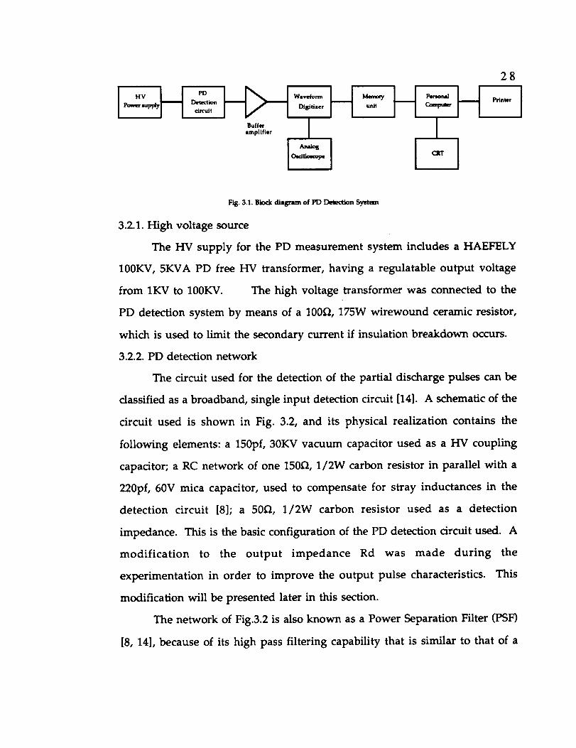
3.1 Block diagram of PD detection system ..................................................... 28
3.2 PD detection network ................................................................................... 29
3.3 AC frequency response of PD detection network ................................... 31
3.4 Response of the high pass RC network .................................................... 33
3.5 Response of the PSF to an exponential pulse across Ct ........................ 37
3.6 Response of the modified PSF to an exponential
pulse across Ct ................................................................................................ 37
3.7 PD detection circuit with modified output impedance ........................ 38
3.8 Calculated AC frequency response of modified PD
detection network ......................................................................................... 39
3.9 Experimental AC frequency response of modified PD
detection network ......................................................................................... 40
V
Page 10
Figure
3.10
3.11
3.12
3.13
3.14
3.15
3.16
3.17
3.18
3.19
3.20
4.1
4.2
4.3
4.4
Page
100 MHz Buffer amplifier ......................................................... . ................. 42
PD data acquisition and analysis system .................................................. 43
A/D transfer function .................................................................................. 44
Sampling time ............................................................................................... 46
Bi - slope triggering mode ........................................................................... 60
Charge injection to sample capadtor ........................................................ 64
High voltage calibration mode .................................................................. 65
Calibration pulse ec ....................................................................................... 68
Response of the PD detection network to a calibration pulse ............. 68
Calibration of the test circuit ...................................................................... 69
Voltage pulse used for calibration ............................................................. 70
Print-out of test 1 results ............................................................................. 74
Pulse used in test 2 ........................................................................................ 76
Typical partial discharge .............................................................................. 79
Test results of specimen #8 ......................................................................... 81
vi
Page 11
CHAPTER 1
INTRODUCTION
1.1. Background
Partial discharges, basically electric discharges that do not produce a
complete bridge between electrodes [1], cause progressive deterioration of an
insulating material and may lead ultimately to insulator failure.
The terms corona and partial discharges have been often used in the
literature to describe the same discharge phenomena [2]. In recent years, the
term corona has been reserved for visible phenomena, that may occur on a
high voltage transmission line [3], or around electrodes at low pressure
conditions [4].
For phenomena that are not visible, because they are internal to a
material or device, the term partial discharge is preferred. In the remaining
chapters of this thesis, these phenomena will be referred as partial discharges
or as PD.
Gas-filled voids or cavities within solid dielectrics are among the most
common sources of partial discharges [5]. These cavities may be produced as a
consequence of process control errors during the production of almost any
type of solid dielectric or liquid-impregnated solid dielectric. Air leaking into
the mold during curing may form a void, or insufficient pressure on the
liquid epoxy during curing may permit a gaseous cavity to develop due to the
vapor pressure of an epoxy component. In addition, foreign particles such as
dirt, paper, textile fibers, etc., in the dielectric may lead to void formation.
The permitivity of the medium in a cavity is frequently lower than
that of a solid insulation, which causes the field intensity in the cavity to be
Page 12
2
higher than in the dielectric. Accordingly, under normal working stress of
the insulation the voltage across the cavity may exceed the breakdown value
and may initiate breakdown in the void.
The significance of partial discharges on the life of insulation has long
been recognized. Every discharge event degrades the material due to the
energy impact of high energy electrons or accelerated ions, which causes
chemical transformations of many types.
The detection of partial discharges is based on energy exchanges which
take placeduringthedischarge. These exchanges are manifested as a)
electrical impulse events; b) dielectric losses; c) electromagnetic radiation
(ligh0; d) sound; e) increased gas pressure; t') heat and g) chemical reactions.
Discharge detection and measurement techniques may be based on the
observation of any of the above parameters [6].
Several measuring systems and techniques have been devised over the
years for partial discharge detection. These techniques encompass from the
simplest and oldest "hissing test", where noise produced by discharges was
used as an indication of their presence in the device under test, as well as
modern digital instrumentation.
Basically, PD measuring systems can be classified as non-electrical or
electrical, depending on which physical parameter associated with the
discharges is measured.
Non-electrical systems measure energy exchange in the form of
chemical transformation, gas pressure, heat, sound and light, the last two
being of more practical importance [1]. There are two disadvantages
associated with the use of non-electrical systems:
Page 13
3
Although they can detect the presence of internal discharges and
their location in a dielectric sample, the discharge magnitude cannot be
directly obtained.
- The testing environment plays an important role in the detection
sensitivity, as in the case of sound detectors testing samples in noisy
environments, where background noise drastically decreases the
detection sensitivity.
The most frequently used and the most successful PD detection
methods are electrical. These methods aim to separate the impulse currents
linked with partial discharges from any other phenomena. The impulse
current is then used to analyze the PD activity in the device under test.
Kreuger [1], identifies four steps that are needed for a complete
correlation of partial discharges with their degrading effect on insulating
materials: detection, measurement, location and evaluation.
Detection refers only to the certainty that discharges are present in the
sample under test. Once a discharge pulse has been detected, its magnitude
must be determined in the measurement stage. A physical quantity (or figure
of merit) which is both relevant to the harmfulness of the discharges and can
be measured with a discharge-detection method must be chosen. For some
apparatus under test, like power transformers and high voltage cables, it is
important to locate the precise source of partial discharges. This is not the
case when testing small devices like capacitors with capacitances of the order
of microfarads, for which the sensing of partial discharges is more important
than pinpointing the PD site [7]. The last step, evaluation, allows an
estimation of the type of danger that the detected discharges represent to the
Page 14
4
insulation being tested, and the information thus obtained is used to predict
the useful life of the sample under specific operating conditions.
This thesis is principally concerned with PD detection and analysis
systems capable of detecting, measuring, displaying and performing an
evaluation of the discharge activity of a device or material under test. Such
systems are often referred to as "PD diagnostic systems"[8]. The information
obtained is then used to get a better understanding of the degrading
mechanisms of PD's.
Two commercially available PD diagnostic systems are most commonly
used:
- PD energy measuring systems using a digital correlator [9, 10]
- Pulse height analyzers [8, 11]
1.2. Problem
Current research and development efforts to improve the ability of the
electrical insulation systems to withstand energy discharges are heavily
dependent on partial discharge diagnostic systems that can provide accurate
and meaningful test data.
The primary purposes of PD analysis in research and development are
basically to:
- Provide an empirical basis to correlate the PD behavior exhibited by
different types of dielectric materials under different test conditions.
- Gain a better understanding of the physical mechanisms related to PD
activity.
There are several experimental findings that support the need for fast
and detailed analysis of partial discharges:
Page 15
5
- Dielectrics under high stress conditions deteriorate due to the effect of
microdischarges that take place in gas-filled voids or cavities within
them [12].
- This deterioration increases with the number of discharges and is
consequently proportional to the frequency of the applied voltage. The
useful life of a dielectric is typically inversely proportional to frequency
[12].
- The number of discharges also increases with increasing electrical
stress in the dielectric. Moreover, the mechanism of deterioration is
affected by electrical stress [13].
From these findings, it is clear that PD measurement systems able to
produce individual pulse resolution from high frequency bursts will provide
valuable data to characterize partial discharges.
There is also a tendency in the design of modern electrical and
electronic systems to further stress dielectric materials:
- In aerospace applications, weight and physical size of electrical
equipment can be reduced by an increase in operating voltages and
frequencies [4]. Consequently, more stringent testing for PD is
necessary in order to assure high levels of reliability.
- Electronic devices like capacitors have to withstand large and fast
switching pulses associated with thyristors and power transistors in
modern power electronics applications [8].
Unfortunately, conventional analog PD detection and analysis systems
are not capable of performing high speed measurements because of their
relatively narrow detection bandwidth ( ~ 10 KHz to several hundred KHz )
Page 16
6
[8]. They have long time constants and in essenceintegrate the detected
signals; individual pulses contribute only to an average value [14].
The development of digital instrumentation has made an important
impact in the development of PD diagnostic systems. In modern equipment,
two techniques are currently used: Pulse height analysis using a Multichannel
analyzer (MCA), and PD energy measurement using a digital correlator.
Although these systems are far faster than conventional analog PD detection
systems, some drawbacks are associated with their performance:
- The processing time for each acquired pulse is made up of two
components: the time required to "shape" a PD pulse by increasing its
rise time before it is processed, in order to comply with the input signal
requirement of the instrument, and the inherent time required for the
instrument to process each pulse. The total time is in the order of
10_tsec for the Multichannel analyzer [15], and 140_ec for the digital
correlator [16].
- The data obtained from each pulse is used to perform a very specific
type of analysis. Once a pulse has been processed no further
inferences can be made about its waveshape.
There is then a need for a real time computer-based data acquisition
system able to perform PD analysis according to the following characteristics:
- Broadband detection systems with capability of individual pulse
resolution without the need of a shaping stage.
- Capability to produce valuable analysis from the individual pulse
data, making it a very flexible system able to produce not only statistical
information related to charge content but also to changes in repetition
rate and waveshape characteristics.
Page 17
- Automatic operation, so it can monitor life tests for long time frames
without human intervention.
- Ease of operation, preferably menu-driven operation, so no
complicated adjustments will be needed before each data acquisition.
- General purpose instrument that can be used to test different
materials or devices under different test conditions.
1.3. Purpose
The purpose of this thesis is to design and build a computer-based PD
diagnostic system having a sampling capability of 200 megasamples per
second and being able to operate in either a manual or automatic mode.
This project has been sponsored by the National Aeronautics and Space
Administration, NASA, as a research project to build a fast PD diagnostic
system to be used in testing materials and devices for future applications at
power frequencies of 20KHz. At this point in the project, the system has been
fully tested at 60Hz and the preliminary testing at high frequency voltages has
been started. The block diagram of the proposed system is shown in Fig. 1.1.
I" H" H)-t""-H- H--'H IPower supply Detection Printercircuit Disitizer unit
•;=, I I
Fig. 1.1. Block diagram of PD Detection System
This experimental system consists of 3 main parts:
a) High voltage source;
Page 18
8
b) PD detection network;
c) Data acquisition and analysis system.
The high voltage source is a 100KV, 5KVA PD free transformer, having
a regulatable output voltage from 1KV to 100KV. The PD detection system is
a RC network performing as a "straight PD detector" [1], where the discharges
of interest are separated from the power frequency voltage and the discharge
pulse voltage across a detection impedance is measured. The data acquisition
and analysis system consists of a 200 MHz digitizer in combination with a 4
Megaword memory unit connected to an IBM compatible computer through
a General Purpose Interface Bus (GPIB). Using dedicated software, the
computer controls the complete operation of the data acquisition system, by
setting the instrument's front panel acquisition controls, analyzing the
digitized data from each pulse and producing statistical analyses of the charge
content of each partial discharge.
Page 19
CHAPTER 2
LITERATURE REVIEW
2.1. Introduction
Commercially available instrumentation for the measurement of
partial discharges has been developed primarily for two applications:
manufacturing quality assurance and service life assessment.
The first one is the largest application for PD measuring equipment,
although a few systems, like the one reported by Boggs [17], have been
developed for PD measurements on installed systems.
Quality assurance covers PD testing during design and manufacturing
of insulated equipment, cables, devices and all electrical systems whose
reliability depends, to a great extent, on their capability to operate satisfactorily
for several years under high field conditions.
PD testing is specified for a very wide range of high field systems, and
high field systems nowadays include even many different types of low
voltage applications, such as integrated circuits which operate at very low
voltages across such thin dielectrics that the phenomena of charge injection
and degradation, usually associated only with highly stressed high voltage
dielectrics, can occur [18]. This means that high electrical stress does not
necessarily require high voltage.
The variety of instrumentation and measurement techniques for
partial discharges is as extensive as the different applications for the materials
and systems to be tested. In some cases of corona in air, the only concern is
radio interference and appreciable levels of PD are tolerable. In other cases,
such as solid dielectric materials used at high stress (> 2.5 KVrms/mm), no PD
Page 20
l0
should be detectable at the highest test voltage and the greatest available PD
detection sensitivity.
In general, and through experience, manufacturers and users now
have a clear understanding of the manufacturing process limitations.
Becauseof this, it is possible to determine the maximum PD level that can be
tolerated and the service life expected for a particular class of apparatus.
An electrical PD measuring system consists basically of two
components: a PD detection circuit and a pulse processing unit. Both have to
operate together as a coordinated system that maximizes the measuring
sensitivity required for the specific type of apparatus or material under test.
Over the years, several combinations of detection circuits and pulse
processing units have been used, and because of the large variety of such
systems, it is rather difficult to make a general classification. Kreuger [19] has
classified the PD measuring systems based on the number of inputs to the
detection circuit. Steiner [14] uses a different approach, making a classification
on the grounds of not only the number of inputs but also on bandwidth of
the detector and method of display information. A literature survey was
conducted in order to determine, as completely as possible, all of the different
commercially available PD measuring systems in use today. In order to cover
this subject in an organized way, we will review detection networks first and
then the complete PD measuring systems.
2.2. Detection networks.
Four basic network topologies are most commonly used for PD
detection:
- RLC networks
- Discriminating circuits
Page 21
11
- Loss detectors
- Differential or balanced detectors
These detection circuits can be classified according to two
characteristics: number of inputs and bandwidth.
A brief description of each one of these basic topologies will be
provided in this chapter. In addition, references to publications where more
detailed information about their performance can be found will be included.
Depending on the number of inputs, a detection circuit can be classified
as: a) single input (or "straight detection method" [1]), where a voltage or
current signal ( and any interference ) is measured at some point of the test
object, and b) multiple input, used to reduce the effect of interference. The
most common multiple input system uses two detection impedances. When
these impedances are similar, the circuit is called balanced. Black [21] presents
a very interesting report on PD pulse detection using balanced networks in
noisy environments.
With respect to bandwidth, PD detection circuits can be classified as
narrowband or broadband. The distinction between them is based upon the
ability of the circuit to resolve individual pulses. If the bandwidth of the
detector is sufficiently wide to resolve individual pulses, then the detector is
considered to be broadband, otherwise it is narrowband.
In general, commercial PD detection systems are bandpass in nature:
the signals of interest are small pulses superimposed on large, power
frequency voltages, and successful detection of the pulses requires separating
them from the power frequency voltages. Narrowband measuring systems
have long time constants and in essence integrate the detected signals;
individual pulses contribute only to an average value [20].
Page 22
12
2-2.1.RLC networks.
The most common circuit used for partial discharge detection is based
on a RLC network. In Fig.2.1, a schematic diagram of a typical RLC PD
detection network is shown. This circuit is implemented basically using a
high voltage coupling capacitor terminated in a measuring impedance.
This combination, also known as the pulse detection network or as the
power separation filter (PSF) [8], has a high pass filtering effect similar to that
of a single pole RC differentiating network. Stray inductances and nonideal
components influence the response of these networks, but their primary
behavior can be modeled as the second order response of an RLC network.
HV 0
Cs
-- Cc
L
o O_tp_t
Fig. 2.1. RLC network
It is important to recognize that the coupling capacitor Cc must be PD
free up to the maximum test voltage used for a particular specimen.
The PSF is a broadband single input detector, used by most PD detection
systems, as reported in [8, 9, 22]. In chapter 3, a detailed description of the
operation of this circuit is provided.
Page 23
13
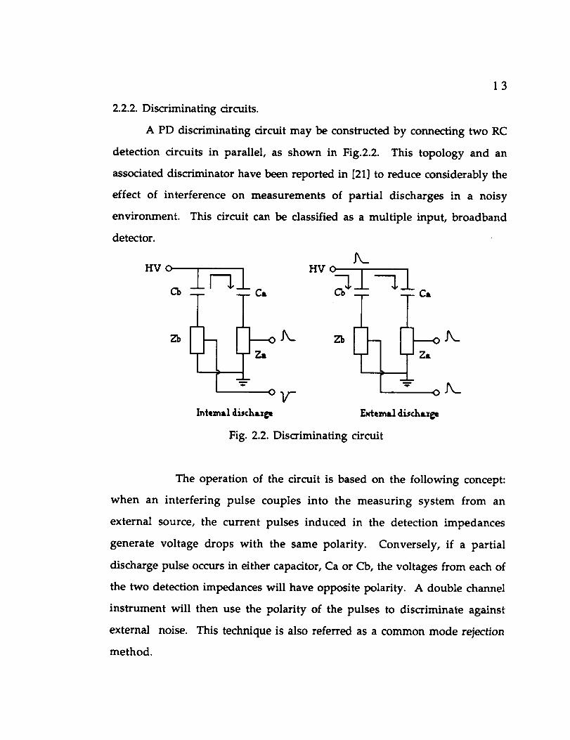
2.2.2.Discriminating circuits.
A PD discriminating circuitmay be constructed by connecting two RC
detection circuits in parallel, as shown in Fig.2.2. This topology and an
associated discriminator have been reported in [21]to reduce considerably the
effect of interference on measurements of partial discharges in a noisy
environment. This circuitcan be classifiedas a multiple input, broadband
detector.
HV 0
6%
Z%
Intez.al 4i*chLx_
HV o
[E.tem..1 di_¢hAxge
Fig. 2.2. Discriminating circuit
The operation of the circuit is based on the following concept:
when an interfering pulse couples into the measuring system from an
external source, the current pulses induced in the detection impedances
generate voltage drops with the same polarity. Conversely, if a partial
discharge pulse occurs in either capacitor, Ca or Cb, the voltages from each of
the two detection impedances will have opposite polarity. A double channel
instrument will then use the polarity of the pulses to discriminate against
external noise. This technique is also referred as a common mode rejection
method.
Page 24
14
This detector improves the sensitivity of partial discharge
measurements in situations where one or more of the following problems
are present:
- The HV transformer is not discharge-free at the operating voltage.
- Corona is present in the external circuit
- The supply line voltage contains pulse interference.
One of the advantages of this system is that the coupling capacitor does
not have to be discharge-free, and may even be replaced by a second test
component. This is possible when the polarity of the pulses is also compared
to the instantaneous applied voltage. Based on the fact that partial discharge
pulses will have polarities that depend on the instantaneous polarity of the
test voltage, the discriminating instrument can determine whether the PD
pulse ocurred across Ca or Cb. If a partial discharge occurs in Ca during the
positive half cycle of the test voltage, a positive voltage is then expected across
the detection impedance connected to Ca.
One of the disadvantages of this system is that strong interference may
cause the the system to block almost completely the processing of signals, and
become almost "blind". This occurs because whenever a noise pulse is
present, the discriminating instrument cannot respond to any incomming
pulses for a time typically of the order of 10 gsec. Consequently, continuous
interference can cause the system to become saturated.
To solve this problem, a subtraction technique is used to reduce the
continuous interference before the signals are processed by the discriminator.
2.2.3. Loss Detectors.
Loss detectors are commonly used to measure the dielectric strength of
insulating materials. Their use is based on the concept that an electrically
Page 25
15
stressed dielectric will exhibit losses due to its inherent conductivity. If partial
discharges are present, they will cause additional changes in the original
values (i.e., with no discharges) of capacitance and dissipation factor of the
specimen under test.
A real dielectric can be represented by the configuration in Fig.2.3a, i.e.,
as a parallel combination of a resistance R and capacitance C. Fig.2.3b is
the vector diagram of the electrical response of the circuit, where angle 0 (or
phase angle) represents the angle by which current leads voltage. If the
conductance of the sample (G), is zero as with an ideal capacitor, 0 is equal to
900; and if C = 0, as for a perfect resistor, then 0 will be equal to 0. From
Fig.2.3b follows that
tan_ = 1 (2. I)_RC
C
7± iT IR
Ira(Y)
°..o° .......
_C
)I) 8 l (Y)
Fig. 2.3. Real dielectric representation
Conduction through a resistor, unlike conduction through a perfect
capacitor, must always cause joule heating. By observation of Fig.2.3b, cos0
Page 26
16
can be related to a measure of the resistive component of the impedance and
hence the rate of heat generation or electrical power absorption. For materials
with very little conduction, cos0 can be considered equal to tanS, which is
commonly referred as the dissipation factor or "loss tangent" of the dielectric.
As reported by Dakin [23], internal discharges in a dielectric will cause
the capacitance and dissipation factor of the sample to change from their
initial values in the absence of internal discharges. This change in the value
of tan8 is commonly used in quality assurance to evaluate the dielectric
strength on stator coils and windings of high voltage rotating machines. The
method is known as "power factor tip up". The validity of the change of tanS,
AtanS, as a measure of PD activity is extensively discussed by Kelen in [24].
Tan8 has a particular advantage as a measure of the quality of a
specimen of insulation: it is dimensionless, and because of this fact, direct
comparisons can consequently be made on similar materials having widely
different geometries [25].
The most common loss detector in use today is the Schering bridge.
Fig. 2.4 shows a schematic representation of the basic configuration of this
bridge.
The specimen dielectric is placed in one of the arms of the Schering
bridge. The value of Atan8 can be obtained by balancing the bridge once
internal discharges are present in the specimen. PD's in the specimen
dielectric ( represented by Zx) will cause an unbalance in the bridge that can be
compensated by an adjustment in the values of R1 and C1. The relationship
between tan8 and the values of impedance Z1 will be found for the balance
conditions:
Zx = Z2. Z3. Y1 (2.2)
Page 27
17
By expanding this expression and equating the real and imaginary terms,
J "J 1 + joG1 ) (Z3)
R2C 1
Rx= C3 (2.4)
and
C3 R1
c_ = R2 (2.5)
By representing the dielectric sample as a parallel combination of a capacitor C
in parallel with a resistor R, as explained above, and using (2.4) and (2.5), the
following relationship can be obtained [26]:
tan8 - 1taRC - taRx cx = °xR1C_ (2.6)
Consequently, by balancing the bridge through the variable capadtance
C1, a reading on the change of tan8 can be obtained, and thus be directly
related to the appearance of partial discharges. In other words, at a voltage
below Vi (PD inception voltage), the measured value of loss tangent
represents the dielectric loss in the solid insulation; above Vi an additional
contribution to the measured value of loss tangent is made by the energy loss
due to partial discharges.
The basic topology of the Schering bridge of Fig.2.4 has been modified
over the years in order to improve sensitivity and eliminate stray
capacitances. A complete discussion of the different loss detectors in use is
given by Baker in [25].
Page 28
± ±
18
I Z1
Fig. 2.4. Schering Bridge
2.2.4. Differential detectors.
Differential detectors are commonly used when individual pulse
resolution is required when testing for PD's in noisy environments.
The test system is configured as a bridge detector, and a basic topology
for this circuit is depicted in Fig.2.5. The device under test is connected in the
specimen arm of the bridge. If the standard capacitor with impedance Zs
is identical to the specimen, the bridge will be balanced. Otherwise, the
variable impedances Z1 and Z2 must be adjusted to reach balance.
When the bridge is balanced, any interference coupled into the system
becomes a common mode signal which induces equal voltages at the detector
inputs. The signal is sensed as a differential voltage across the detection
transformer, so any common mode signals cancel.
A variation of this topology, known as a differential bridge, is shown in
Fig.2.6. In this circuit, balance is achieved by changing only the transformer
turns ratio, making this detector very easy to balance.
Page 29
HV?
-- ZC
T
m
Detectoz
.J_
19
Fig. 2.5. Differential detector
The disadvantage with this network is that large currents in the
specimen will also flow through the detection transformer, and construction
of a precision wideband transformer of the quality required in a bridge
detector with adequate current capacity is difficult.
HV
7
l DetectozZs _ Zcl- -
Fig. 2.6. Differential bridge
2.3. Pulse processing instruments.
Pulse processing instruments can be classified according to the way in
which the pulse information is processed and displayed. Three basic types can
be identified:
Page 30
2O
- Direct display
- Meter display
- Computer-based systems
2.3.1. Direct display.
A direct display instrument operates like an oscilloscope; the detected
pulse is displayed directly on a CRT. One of the most common direct displays
used for PD detection has an elliptical time base mode, in which the partial
discharge pulses are displayed around the perimeter of an ellipse. The
ellipse is displayed in such a way that top and bottom coincide with the
positive and negative peaks of the high voltage sine wave and the ends
coincide with the zero crossings. The discharge patterns displayed in
this way give a good indication of the type and source of the partial
discharges. Standard discharge patterns can be found in the instruction
manuals for commercially available instruments using this type of display
[27].
2.3.2. Meter display.
This type of display is associated with integrated measurements and is
implemented as a digital panel meter or as an analog meter movement.
The information provided is a quantity related to partial discharge
activity, the most common being the PD charge content in Coulombs.
Instruments like the HAEFELY PD detector [27] use a meter display to
complement simultaneously its elliptical time base display.
2.3.3. Computer based systems.
The development of digital instrumentation has made possible
significant advances in the knowledge of the degradation mechanisms of
partial discharges; the PD pulses are not only "seen" on the screen of the
Page 31
21
oscilloscope but can also be detected individually and their waveform
characteristics can be stored in digital form to be used later for a great variety
of analysis.
The most common commercially available computer-based
instruments under this classification are digital correlators and pulse height
analyzers.
2.4. Computer-based PD diagnostic systems.
2.4.1. Digital correlator.
Some investigators [9, 10] have reported the use of a digital correlator to
measure energy instead of charge as a figure of merit for PD. This method is
based on the fact that energy is an inherent property of the discharge, and that
an energy supply is essential to sustain a degradation process.
The measurement of energy is carried out by an evaluation of the
following expression:
N
Et = _ Ui Qi (2.7)
i=1
where Et is the energy supplied by the source over the time period t
during which N discharges have been produced, Qi and Ui being respectively
the apparent charge of discharge i and instantaneous value of the applied
voltage at the moment of the discharge.
This summation of products is performed by using the analysis
characteristics of a digital correlator. This instrument is basically a signal
analyzer capable of computing and displaying 100 points correlating
functions. A complete description of the digital correlator, which is beyond
Page 32
22
the scope of this report, can be found in [16]. The important feature of the
digital correlator is its ability to perform a mathematical operation with the
following characteristics:N
1Rxy(¢) = _- _ x ( k At - x ). y ( k At ) (2.8)
k=l
where x and y are the two waveforms to be correlated, N is the number of
times the evaluation will take place (or number of samples taken), x is the
delay time used for correlation purposes and At the sampling rate. The
instrument is able to perform the above calculation for 100 different values of
x, but for the specific application of the PD energy measurement, only the case
for which _ is equal to zero is of importance. Waveforms x and y will be
identified with Ui and Qi, respectively.
In Fig. 2.7, a topology for pulse detection and simultaneous
measurement of the instantaneous value of the applied voltage is provided.
As can be observed, the pulse detection arm of the circuit is basically a power
separation filter, as described earlier in this chapter.
C1
C2
i D
!
m
IoUb
Fig. 2.7. Pulse detector for PD energy measurement
Page 33
23
Although the concept presents very interesting possibilities for the
measurement of PD energy instead of charge, the instrument requires a
minimum of 140 ttsec to evaluate each pulse. Consequently, it is unable to
process pulses that occur with a frequency greater than 7 Khz.
2.4.2. Pulse height analyzers.
In conventional Partial discharge measuring systems, as described in [8,
11, 28], pulse height analysis is extensively used.
This type of analysis is performed by commercially available
instruments known as single channel analyzers (SCA) or multichannel
analyzers (MCA).
These instruments classify a pulse by its height within certain
preselected ranges, and the output of the analysis is a count of the number of
pulses that occurred within these ranges or intervals. Internally, the
equipment converts the height of the pulse (in Volts) to a charge level (in
Coulombs). If the analysis is made by sampling one channel at a time, the
apparatus is called SCA. Thus, the SCA is capable of recording only those
pulses falling within a single channel or section of an energy spectrum; all
other pulses are rejected. In Fig. 2.8 a block diagram of a typical SCA is shown.
Uppez level discziminatoz
IM,e i,m [ l.i_ea,
detectox [ Amplitiex)
ULDle_l E + AE)
LLD(h,,,1 Z)
Iarw,ez level disczimmatoz
Fig. 2.8. Block diagram of single-channel analyzer (differential mode)
Page 34
24
A significant limitation of the SCA, is its inability to perform a
complete analysis of an energy spectrum in a reasonably short time, because
in order to cover n channels, one must examine sequentially point by point n
individual channels, and this process takes a long time. Consequently, this
equipment is not useful for complete PD measurements over long periods of
time.
• In most practical PD detection systems, a MCA is used to perform pulse
height analysis. MCAs help to avoid the limitations of the SCAs by making
possible a faster scan analysis of an energy spectrum.
The basic principle of operation of the MCA involves an analog to
digital converter (ADC) as developed by Wilkinson, Hutchinson and Scarot
[15, 28]. The process can be summarized as follows: first, a small capacitor is
charged up to the peak of the incoming pulse; it is then discharged at constant
current. While the discharge is in progress, clock pulses from a stable
oscillator are counted by a scaler; the number of clock pulses counted is
proportional to the time the capacitor takes to discharge, and hence to the
original height of the pulse. This process is depicted in Fig. 2.9 [15].
The ADC converts the pulse height to a number proportional to the
energy of the event. This number identifies a dedicated memory location,
and one count is added to the contents of that memory location.
After data have been collected for some period of time, the memory
contains a set of numbers that correspond to the number of pulses in each
energy level bin.
As expressed in [28], the MCAs are capable of recording most of the
pulses associated with an energy spectrum. The only pulses not recorded are
those that occur while the analyzer is busy handling a previously acquired
Page 35
25
pulse. The time required for the MCA to process one single pulse is in the
order of 10_sec.
I_p_t
sisal -
Crystal co_txolledpulse tzLiw
Fig. 2.9. ADC Ramp and pulse train
The above description and the technical data of commercially available
MCAs lead to three important aspects of MCA performance for our
investigation: first, pulses having fast risetimes (< 1 _sec as specified for the
CANBERRA Series 35 PLUS Multichannel Analyzer [15]) must be "shaped"
prior to being input to the instrument in order to increase the rise time of
those pulses. As described in [8], a pulse-shaping amplifier can be used to
increase the magnitude and duration of the incoming pulses.
Second, the MCA is not able to process all incoming pulses from a
high frequency burst, because of the time required to evaluate each one of
them. And finally, once the information about the pulse height of a
single pulse has been obtained, no information is available about the shape of
the pulse, so no further conclusions about changes in the characteristics of the
waveshapes under different test conditions can be drawn.
Page 36
26
2.5. Conclusions from the literature review:
1. A dielectric under high stress conditions deteriorates due to the effect of
microdischarges that take place in gas-filled voids or cavities contained
within it.
2. These cavities are produced in most casesdue to process control errors
during the production of almost any type of solid dielectric or liquid-
impregnated solid dielectric.
3. Partial discharges produce reduction in the useful life of a dielectric
material. Consequently, a need to detect, measure and analyze the nature of
those discharges has arisen.
4. Several measuring systems and techniques have been devised for partial
discharge detection. Detection schemes which are most sensitive tend to be
application specific, while those which are of general applicability tend to
sacrifice some sensitivity.
5. Basically, PD detection systems can be classified as electrical and non-
electrical. Electrical systems are more commonly used.
6. The bandwidth of the detection system limits the quality of the information
that can be obtained. For research and development purposes, systems
capable of single pulse resolution are preferred.
7. Two commercially available instruments most commonly used for PD
analysis are Multichannel analyzers and Digital correlators.
8. These instruments present processing time constraints due to the "dead"
time associated with the processing of an individual pulse.
9. There is a need for fast computer-based PD diagnostic systems in order to
study PD degrading mechanisms in highly stressed dielectrics exposed to high
voltage and high frequency AC power sources.
Page 37
CHAPTER 3
DESCRIPTION OFTHE SYSTEM
3.1. Introduction
Most of the PD diagnostic systems in use today are based on the concept
of pulse height analysis, although some investigators have reported the use
of a digital correlator to perform PD energy measurements [9, 10]. Two
important disadvantages limit the quantity and quality of the data obtained by
using those instruments: a) the time required to process each pulse could
easily prevent a large number of pulses from being analyzed for high
frequency burst sources, and b) the data of each waveform cannot be stored for
further experimental work to correlate pulse characteristics with time, cavity
size and shape, dielectric material and frequency of the AC source.
In this thesis, a new PD measurement and analysis system is described.
Its overall characteristics and flexibility of operation make it a suitable option
for long duration test experiments, needed to increase the understanding of
the effect of PD's in the aging process of dielectrics.
3.2. General description
This new experimental system consists of 3 main parts:
a) High voltage source;
b) PD detection network;
c) Data acquisition and analysis system.
A block diagram of this system is shown in Fig. 3.1. The high voltage
source and detection network were located inside ASU's high voltage
laboratory, a completely shielded room acting as a Faraday cage [29].
Page 38
° H>-t""-H "-H HPower sul_y Detection Digitizer unitcircuit
• 1 1
28
Printer
Fig. 3.1. Block diagram of PD Detection System
3.2.1. High voltage source
The HV supply for the PD measurement system includes a HAEFELY
100KV, 5KVA PD free HV transformer, having a regulatable output voltage
from 1KV to 100KV. The high voltage transformer was connected to the
PD detection system by means of a 100_, 175W wirewound ceramic resistor,
which is used to limit the secondary current if insulation breakdown occurs.
3.2.2. PD detection network
The circuit used for the detection of the partial discharge pulses can be
classified as a broadband, single input detection circuit [14]. A schematic of the
circuit used is shown in Fig. 3.2, and its physical realization contains the
following elements: a 150pf, 30KV vacuum capacitor used as a HV coupling
capacitor; a RC network of one 150_, 1/2W carbon resistor in parallel with a
220pf, 60V mica capacitor, used to compensate for stray inductances in the
detection circuit [8]; a 50_, 1/2W carbon resistor used as a detection
impedance. This is the basic configuration of the PD detection circuit used. A
modification to the output impedance Rd was made during the
experimentation in order to improve the output pulse characteristics. This
modification will be presented later in this section.
The network of Fig.3.2 is also known as a Power Separation Filter (PSF)
[8, 14], because of its high pass filtering capability that is similar to that of a
Page 39
29
single pole RC differentiating network. Stray inductances and nonideal
components influence the response of these networks; so in the physical
realization of the circuit the following considerations were observed in order
to reduce the effect of stray elements:
- The leads of all elementswere kept as short aspossible.
- Carbon resistorswere used instead of wirewound ones,becauseof
their inherently smaller inductance.
- Elements C1, R1, Rd, D1 and D2 were all contained within a small
metallic box which structure was connected to the system ground.
lOOn, 175w
HVRI
Cs E_
S_m_lec*picitoz
±Cc lS0pt
30KVT
1,/2W R1 C1 60V
I o O_tp_t
D1 _ t P_ sonD2 I 1/2W
_J_t
Fig. 3.2. PD detection network
In order to protect the measuring instrument from high amplitude
transient pulses, that can be generated at the breakdown of a sample or by the
switching of the HV supply, two zener diodes D1 and D2 with minimum
breakdown voltage of 25V were connected as shown in Fig. 3.2.
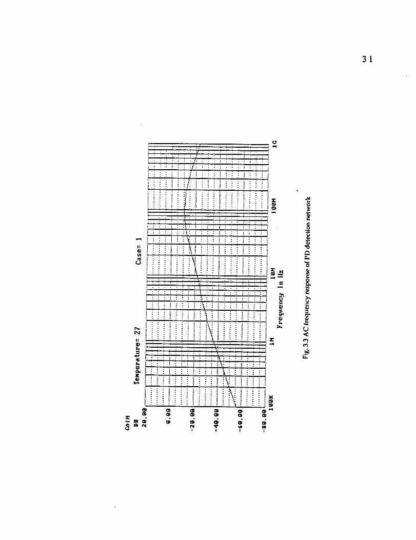
The AC frequency response of this circuit was calculated with PSPICE
4.04, a circuit simulator, by sweeping an AC input signal from 1KHz to 1GHz.
Page 40
30
The results of this simulation are presented in Fig.3.3, and the listing of the
PSPICEfile used to generatethis responsecan be found in Appendix A.1.
The cut-off frequency (lower 3dB frequency) of the circuit can be found
from [28]:
f _ 1 - 21.22 MHz (3.1)
2 7t R d C c
where C c = 150pF and R d - 50f2. Elements C1 and R1 do not affect appreciably
this value, as can be observed in Fig. 3.3. These results indicate that the 60 Hz
power frequency voltage is expected to be attenuated by:
flA = - 20 log _ = - 110.97 dB (3.2)
were fl = 21.22 MHz and f2 = 60 Hz. Experimentally, the attenuation observed
was - 109.03 dB, a value consistent with the theoretical results expected.
An analysis of the behavior of this circuit as a high-pass RC network to
4 different input signals at node 1 was prepared using the following functions:
a) sine-wave; b) step-function (step-voltage); c) pulse input and d) exponential
waveform.
3.2.2.1. Sine-wave function
If vi is a sine-wave of frequency f applied across the combination in
series of capacitor Cc and resistor Rd (the simplest representation of our
power separation filter), the output Vo at Rd represented as a function of
frequency is:1
(3.3)
Page 41
31
i iiii iiiiiiiiiiii
.... i-.-;:.
• • • • . . . o t . ° z
iiiil l-_:::i::i;ii!i
iiiil :i:::_:::!i!:_
::::::::::::::::::::::
_ • • • _ . • _ . . . ...
_ iiiii!i :::i::: :::_ : : : , : : : : : j : : : i : : : :i " : : i : "- : : : z : : : : : :
: i!!!::!!!.! : • " i _
! : : : i : : : i "" _""" :" • • _
i : : : i : : " -' : : "_ " " " : " ' " i
:I" " : " " " : " " " _ -• ° . . _ ° . •
...... . . _ • ! . . . . : : : _ _J
i : : : i : : : i : :', : : : : : - " t.
! ....... ! I : : : _ : : : _.g3
' : : • i • " " \ : : i "_1.. : : : :: i :::i _ i! i _. • . . _ • o :
, . . • .... _ ! : i : : :_,., _ : ! : ..' : : : _ : : : _ • _ ....- : • • • i
i i : : i : : : i : : : i _i_:i i : : : 1...... . : : _ : : : _ - . . _ : : :..... : • . : : Ji:::!::.!--._ _!i'_
i " " , : ::_ : _! : : : _
J I I I
Cv
e-0
"0
C_r..,
o
e-
(,e)
L_
Page 42
32
where the denominator ( 1 + (fl/f)2) 1/2 is the magnitude of gain of the
network and fl is the lower 3-dB frequency equal to 1/2_ RdCc as mentioned
earlier. At the frequency fl the magnitude of the capacitive reactance is equal
to the resistance Rd and the gain is 0.707. A Bode plot representing the
response of the circuit is presented in Fig. 3.3.
3.2.2.2. Step function
The response of this RC network to a step-voltage input is exponential,
with a time constant ¢ = RdCc. The output voltage has the form:
t
v 0 =vf +(v i -vf)e _ (3.4)
where vf and vi are the final and initial output voltages, respectively of the
step-voltage function. For t > 0, the input is a constant, and since Cc blocks the
dc component of the input, the final output voltage is zero, or vf = 0. Then
equation 3.4 becomes:
V 0 =v. el
t
RC (3.5)
3.2.2.3. Pulse input
If the pulse in Fig. 3.4a is applied to the RC network, the response for
times that are less than the pulse duration tp is the same as that for the step
voltage input. At the end of the pulse, the input falls abruptly by the amount
V, and, since the voltage at Cc cannot change instantaneously, the output
must also drop by V. Thus immediately after t = tp ( or at t = tp ÷ ), Vo = Vp - v;
Vo becomes negative and then decays exponentially to zero. For t > tp, Vo is
given by:tp (t - tp)
v 0=v(e RC.1) e RC (3.6)
Page 43
33
If RdCc >> tp, there is only a slight tilt to the output pulse and the
undershoot is very small, as shown in Fig. 3.4b. If RdCc << tp, the output
consists of a positive spike of amplitude v at the beginning of the pulse and a
negative spike of the same size at the end of the pulse, as shown in Fig. 3.4d.
3.2.2.4. Exponential input
In any RC network, vi = q/C + Vo, where q is the capacitor charge.
Differentiating this equation gives:
dvi i dv0 dvi v0 dv0
dt -C c + d'-_- or dt -R dC c + dt(3.7)
Suppose the input of the network is an exponential waveform given
t
v. = v( 1 - e _ ) (3.8)!
where z is the time constant of the input wave. Then equation 3.7 becomes:
t v0 dv °v -¥_ +_T e Rd C c dt
(3.9)
Defining n and x by n = RdCc/z and x = t/z, the solution of equation 3.9 [35],
subject to the condition that the capacitor voltage is initially zero, is given by
x
n___X_v.(e n _e-X) (3.10)Vo=n. 1
if n _ 1 and by
v 0 = v x e "x (3.11)
ifn = 1.
Near t = 0, the output follows the input.
smaller the output peak at Rd.
Also, the smaller RdCc is, the
Page 44
34
aJ
Q_
B
X
,.-,j
,,D
c_
Q_u_
e-i
m
_o°_r_L
OJ
0
I
/
_ C
,F.., 0
AA
w_
E Je-
_ o_
_J,.I=
C_
oJ "_"
_0
I
Page 45
35
L_
C_r',X
C
c__J
q_
C_
L_C
L
OJE
°_
L_
I
C
0
L_
!
"5
N
rJ_
J
C
L_
u'_
L_'_
(._
L_
Ls_ _
T
V
L_
_ r
L_
°--q _,Do_
C_
r_
Page 46
36
If the value of the coupling capacitor is fixed, along with all the
parameters in the circuit including stray capacitances, the resistor Rd will
determine the response of the circuit. Unfortunately, increasing the value of
Rd from 50_ produces a mismatch of impedances with the measuring
instrument. An effort was conducted to improve the response of the circuit
by modifying the detection impedance without producing ringing of the
signal. In order to simulate testing conditions, exponential waveforms were
used as input signals to the network.
It is reasonable to assume that typical partial discharges will have
characteristics close to an exponential waveform, with fast risetimes and long
decay times [12]. Consequently, an input signal having a risetime in the order
of 5 nsecs, and decay time of 100 nsecs was applied to the detection system
across the terminals of the sample capacitor to sense the expected response of
the circuit to PD's. This response was obtained using PSPICE 4.04, and the
input and output waveform are shown in Fig. 3.5. The characteristics of the
exponential waveform used in the simulation were determined from the
characteristics of actual PD's observed and recorded in previous tests.
With a change in the output impedance in the PD detection circuit, the
characteristics of the original pulse were recovered with satisfactory result.
When using an input signal with the same characteristics as in the case
presented in Fig. 3.5, the output signal obtained with this new arrangement
had characteristics closer to the original waveform, as can be observed in Fig.
3.6.
The major change made in the circuit was the substitution of a cascaded set of
three high-pass RC filters, as depicted in Fig. 3.7, for the 50ft detection
Page 47
_PDO50TDate/Time run: 02/05/91 _6:54:30 Temperature: 27.0
2. OV+ .................. +- ................. _- ................. 4- ..................
37
1.6v$
i
t
0.Sv _-
O._V
O,OV
-O._VOns
o v (i}
• • • L I'
"4"- '4'-- =4-
50ns lOOns 150ns 20Ons• v(3)
T3me
Fig. 3.5 Response of the PSF to an exponential pulse across Ct
wPD310kDate/Time Pun: 02109/91 11:07:28 lemDerature: 27.0
2.Dr + .................. 4- ................. +- ................. _ ................. -+
1.2V +
O.BV- I-i*
I
o
0"4Viii
0.0v-_ 4-Q*
ii
-O._V+ .................. +- ................. _ ................. _ .................Ons 50ns lOOns ! 50ns 2DOns
ov{l} -v(S)Time
Fig. 3.6 Response of the modified PSF to an exponential pulse across Ct
Page 48
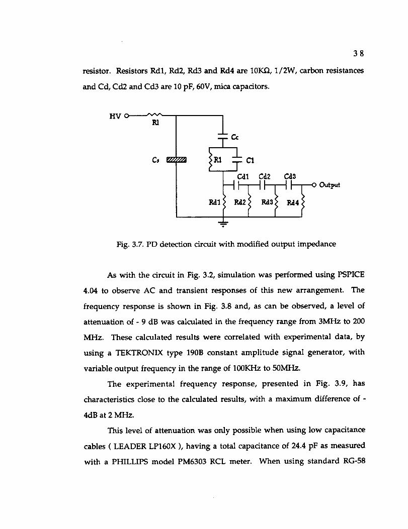
38
resistor. Resistors Rdl, Rd2, Rd3 and Rd4 are 10K_, 1/2W, carbon resistances
and Cd, Cd2 and Cd3 are 10 pF, 60V, mica capacitors.
HV
C_ z_
Fig. 3.7. PD detection circuit with modified output impedance
As with the circuit in Fig. 3.2, simulation was performed using PSPICE
4.04 to observe AC and transient responses of this new arrangement. The
frequency response is shown in Fig. 3.8 and, as can be observed, a level of
attenuation of - 9 dB was calculated in the frequency range from 3MHz to 200
MHz. These calculated results were correlated with experimental data, by
using a TEKTRONIX type 190B constant amplitude signal generator, with
variable output frequency in the range of 100KHz to 50MHz.
The experimental frequency response, presented in Fig. 3.9, has
characteristics close to the calculated results, with a maximum difference of -
4dB at 2 MHz.
This level of attenuation was only possible when using low capacitance
cables ( LEADER LP160X ), having a total capacitance of 24.4 pF as measured
with a PHILLIPS model PM6303 RCL meter. When using standard RG-58
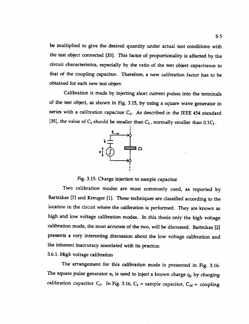
Page 50
4O
!lJ!i!tlt_
!!11!!11
!JrIi
I
,11Illil,!ttlillllII I
IIit
iillljl,!,
!lii_il I'liiii I
Iit
ll!li_l===
QD
II
I
N
tl
_v
c-O
r.,
E
e-
b.
t-
U<m
w
E-=
X
E
(qp) uo!]enue_V
Page 51
41
coaxial cable, a capacitance of 28.5 pF/ft is expected, and 5 feet of this cable
produced -16dB loss experimentally in the same range of frequencies and
under the same test conditions.
One of the problems found in the new arrangement was the distortion
of the output signal due to ringing. This effect was produced by signal
reflection due to the mismatch of impedances between the detection circuit
and the input impedance of the instrument.
With a low input impedance (50£2) at the instrument, the ringing effect
disappeared, but this arrangement was undesirable, because the high output
impedance (10K£2) of our detection circuit had no effect on the output signal
characteristics, because it was shunted by the instrument's low impedance.
An impedance matcher presenting a high input and low output
impedance was connected between the PD detection circuit and the
instruments. This circuit permits a pulse to be sensed across the PD detection
circuit output impedance, and the input of the instrument can be set to 50£2,
to match the coaxial cable impedance.
This circuit has the required characteristics needed for our specific
applications: high input and low output impedances, fast slew rate and broad
bandwidth. The key element in this circuit is a National Semiconductor
device LH0063. A diagram of this amplifier circuit is given in Fig. 3.10.
This amplifier has a gain of 1 for a bandwidth of 100 MHz, and
produces excellent results for matching of impedances between the detection
resistance and the instrument's low input impedance (50£2). The only
limitation found when using the LH0063 is its inherent dc offset of 5mV.
This component can be compensated at the data acquisition stage, as will be
explained in the next chapter. New amplifiers with virtually no output dc
Page 52
42
components are now been investigated, like the AVANTEK GPD 462, with a
frequency bandwidth of 200 MHz, a constant gain of 9dB and with the
advantage that only one dc source is required to power it.
I2-I0060
det&ho_ _ output
impecl,,_ce 50C_ _ 50 CA
-1S'V
Fig. 3.10. 100MHz Buffer amplifier
RC detection topologies are most commonly used to resolve individual
PD pulses when testing in controlled experimental environments, that is,
assuming that the following conditions are satisfied in the testing facilities:
- The HV transformer is discharge free at the testing voltage;
- Corona is not present in the external circuit;
- The supply line voltage does not contain high frequency interference;
- The coupling capacitor is PD free at the testing voltage.
To make sure these assumptions were valid in our laboratory, the
system was tested at high voltage with the sample dielectric C s removed.
The applied voltage was increased gradually and a TEKTRONIX 2430A
digital oscilloscope was used to monitor discharge activity across the detection
impedance R d. No pulses were detected up to 8.5KV rms; beyond that
voltage, small pulses with an amplitude of less than 2mV were observed.
Page 53
43
3.2.3. Data acquisition and analysis system
The heart of the proposed PD diagnostic system is the data acquisition
and analysis stage. This subsystem consists of the following elements:
a) Real time waveform digitizer;
b) Fast Data Cache;
c) General Purpose Interface Bus (GPIB);
d) IBM compatible computer;
e) Software (ASUPD v.1.7).
A schematic of the data acquisition system is shown in Fig. 3.11.
9503 Fast Dit. CAche
CH2 iw
Fig. 3.11. PD data acquisition and analysis system
Before we attempt a description of the different parts of the system, it is
important to mention some theoretical aspects of analog-to-digital (A/D)
converters, to provide a better understanding of the terminology involved in
data acquisition systems.
Page 54
3.3.Data acquisition systemstheory
The following is a basic introduction of data acquisition theory.
44
The
author found extensive information in [28, 30, 31]. The areas to be covered in
this section are quantizing, sampling and coding theory.
3.3.1. Quantizing theory
Analog to digital conversion is basically a two-step process: quantizing
and coding. Quantizing is the process of transforming a continuous analog
signal into a set of discrete output states. Coding is the process of assigning a
digital code word to each of the discrete output states. For example, in a 3-bit
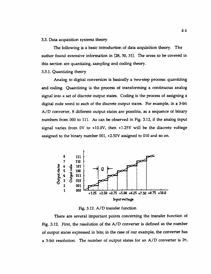
A/D converter, 8 different output states are possible, as a sequence of binary
numbers from 000 to 111. As can be observed in Fig. 3.12, if the analog input
signal varies from 0V to +10.0V, then +1.25V will be the discrete voltage
assigned to the binary number 001, +2.50V assigned to 010 and so on.
$ 111
? 110
_ 6 _ 101100
$ _ 011
0 o 010
2 0011 000 |
+1.25 +2,S0 +O.TS +S,O0 +6.25 +7.SO +8,?S +10.0
Input wltL_
Fig. 3.12. A/D transfer function
There are several important points concerning the transfer function of
Fig. 3.12. First, the resolution of the A/D converter is defined as the number
of output states expressed in bits; in the case of our example, the converter has
a 3-bit resolution. The number of output states for an A/D converter is 2n,
Page 55
45
where n is the number of bits. Consequently, an 8-bit converter has 256
output states, and a 10-bit converter has 1024 output states. As shown in Fig.
3.12, there are 2n-1 analog decision points in the transfer function. These
points are for example voltages +0.625 and +1.875, where +1.25 is the center
point of the output code word 001. The analog decision point voltages are
precisely halfway between the code word center points.
At any part of the input range of the A/D converter, there is a small
range of analog values within which the same output code word is produced.
This range is the voltage difference between two adjacent decision points and
can be found from the following expression:
Q_ FSR (3.12)2 n
where FSR stands for "Full Scale Range", or 10.0V in our example, and n is
the number of bits of resolution of the A/D converter. Evaluating (3.12) with
the values given in our example, Q is equal to 1.25V. In this expression, Q
represents the smallest analog difference which can be resolved, or
distinguished by the converter. If the number of resolution bits is increased,
this error is much smaller. For example, if n=10, the error in our case will be
reduced to 9.76mV.
3.3.2. Sampling theory
An A/D converter requires a small, but significant, amount of time to
perform the quantizing and coding operations. The time required to make
the conversion depends on several factors: the converter resolution, the
conversion technique, and the speed of the components employed in the
converter. The conversion speed required for a particular application
Page 56
46
depends on the time variation of the signal to be converted and on the
accuracydesired.
Conversion time, also known as aperture time or sampling time [30,
31], refers to the time uncertainty (or time window) in making a
measurement and results in an amplitude uncertainty (or error) in the
measurement if the signal is changing during this time.
As shown in Fig.3.13, the input signal to the A/D converter changes by
a value of AV during the sampling time ts in which the conversion is
performed.
1 .... o
is
Fig. 3.13. Sampling time
This difference can be considered an amplitude error or a time error;
the two are related as follows:
dV(t) (3.13)AV = t s dt
where dV(t)/dt is the rate of change with time of the input signal. For the
specific case of a sinusoidal input signal, for example, the maximum rate of
change occurs at the zero crossing of the waveform, and the amplitude error
is:
AV = t s atd ( A sincot )t - 0 = ts Ac0 (3.14)
Page 57
47
The resultant error, expressed as a fraction of the peak to peak full scale
value is:
AVE- 2A - _ f ts (3.15)
This result indicates that the sampling time required to digitize a 1 KHz
signal to a 10 bits resolution is:
E _ 320 nsecs. (3.16)ts- _f
where e is one part in 210 or approximately 0.001.
3.3.3. Coding theory
A/D converters interface with digital systems by means of an
appropriate digital code. While there are many possible codes to select, a few
standard ones are almost exclusively used with data converters. The most
popular code is "natural binary", or straight binary, which is used in its
fractional form to represent a number:
-1 2-2 -3 -nN=a12 +a 2 +a32 +...+an2 (3.17)
where each coefficient "a" assumes a value of zero or one, and the resulting
value N has a fractional value between zero and one. As an example,
consider a binary fraction that would be normally written as 0.110101. With
data converter codes the decimal point is omitted and the code word is
written 110101. This code word represents a fraction of the full scale value of
the converter and has no other numerical significance. The binary code word
110101 therefore represents the fraction 0.82775, where n = 6:
Page 58
1 x 2"1 = 0_5
1 x 2.2 = 0.25
0 x 2.3 = 0.0
1 x 2-4 = 0.0625
0 x 2.5 = 0.0
1 x 2-6 = 0.01525
0.82775
48
or 82.77% of full scale of the converter. If full scale is +10V, then the code
word represents +8.2775V. The natural binary code belongs to a class of codes
known as positive weighted codes, since each coefficient has a specific
positive weight. The leftmost bit has the most weight, 0.5 of full scale, and is
called the most significant bit, or MSB. The rightmost bit has the least weight,
2 -n of full scale, and is therefore called the least significant bit or LSB. The bits
in a code word are numbered from left to right from 1 to n.
The LSB has the same analog equivalent value as the quantizer error
Q, that is:
LSB - FSR (3.18)n
2
An important point to notice is that the maximum value of the digital
code, namely all l's, does not correspond with analog full scale but rather
with one LSB less than full scale, or FSR x ( 1 - 2 -n ). Consequently, a 10-bit
resolution converter with a 0 to +10V analog range has a maximum possible
code of 11 1111 1111, and this number represent a maximum analog value of
+10 ( 1- 2-10 ) = +9.99023V. In other words, the maximum analog value of the
converter, corresponding to all l's in the code, never quite reaches the point
defined as analog full scale.
Page 59
49
3.4.Operation of the PD acquisitionand analysis system proposed
A PD pulse across the detection impedance of the RC network will be
present at one of the input channels of the waveform digitizer. If this pulse
reaches a predefined voltage level,a triggerpulse will be generated internally
in the digitizerand a sampling and recording process will start.
The A/D stage produces a stringof binary code values, or "record",that
represents the original analog pulse voltage waveform. This string of binary
code data is stored temporarily in memory. The number of elements in this
array depends directlyon the memory size assigned to itby the user, as itwill
explained below in the description of the instruments.
Once all the data points of a memory record have been acquired, the
digitizerwill hold until a new triggerpulse isgenerated to startacquisition of
another pulse. This process will repeat until all the predefined number of
records have been acquired and stored.
When all the required number of pulses have been recorded, a data
transfer between the memory unit and the PC will start,one PD pulse record
at a time. The PC will analyze the data of the transfered string,and produce
statisticalinformation related to peak voltage value and charge content per
pulse.
In the case of peak value of the pulse, the maximum binary value
found in the array, either positive or negative, will be "scaled" to its analog
equivalent voltage value. The total number of pulses acquired will be
distributed according to their respective amplitudes. This is accomplished by
setting the number of bin levels n to be used for comparison purposes and
incrementing a count value assigned to each pair of bin levels according to
the actual amplitude of the pulse being analyzed. For example, if the
Page 60
50
amplitude of a pulse P1 is greater than the bin level L1 but smaller than the
immediate superior bin level L2, where L1 and L2 are two consecutive bin
levels, the count assigned to the pair L1-L2 will be increased in one unit, to
indicate that the PD pulse acquired had an amplitude within L1 and L2.
For charge content of the pulse, the absolute value of the peak voltage
will be multiplied by the calibration factor of the particular sample under test.
The calibration process will be discussed later in this chapter. As in the case of
the peak voltages, the number of bin levels n for charge comparisons is also
provided. The charge content of the pulse under analysis is compared with
successive bin levels, and a count is increased accordingly.
Once the analysis has been completed, a measurements file containing
the count values of all the bin level pairs can be sent to a printer.
3.5. Description of the instruments
3.5.1. Real Time Waveform Digitizer
The waveform digitizer used was a fully programmable TEKTRONIX
RTD 710 digitizer, whose electrical specifications are given in Table 3.1. More
detailed technical information about this instrument can be found in [31, 32].
The RTD 710 acquires an incoming analog waveform through
channels 1 and/or 2, producing a digitized stream of information that can be
sent to an external memory unit for further analysis.
The sampling rate will determine how closely the digitized
information will represent the original analog waveform. Depending on the
particular application, different sampling rates can be selected. For this
particular digitizer, a maximum sampling rate of 100 MHz (10nsecs) is
possible in dual channel mode, or 200 MHz (5nsec) in single channel or
"Channel 1 only" mode. An explanation for this difference is the following:
Page 61
51
TABLE 3.1
TEKTRONIX RTD 710 Waveform Digitizer
Electrical Specifications
Input Channels:
Input Range:
Analog Bandwidth:
AC - coupled lower -3dB point:
Input impedance:
Internal clock frequency:
Sample rate:
2, single ended. Supports X10
and X100 encoded probes for
high input voltage applications
+ 100 mV to_+ 50 V (200 mV to
100 V p-p ) in 28 steps.
DC to 100 MHz
10 Hz or less
1 Mr2 + 2%; 24 pF
200 MI--Iz + 0.001%
Single channel mode, 200MS/s;Dual channel mode, 100MS/s.
Page 62
52
when the digitizer operates in dual channel mode, one sample acquired at
channel 1 requires, as a minimum, a processing time of 5 nsecs. The sample
to be acquired then at channel 2 will require another 5 nsecs, consequently,
every sample at each channel takes a total of 10 nsecs.
The RTD 710 allocates a total of 32K 10 bit words of memory for each
channel. This memory is quite flexible; it can be divided into smaller record
lengths (1K, 2K, 4K, 8K or 16K).
The number of records available in dual channel mode can vary from
one record (with 32K word length) to 32 records ( with 1K length each). In our
application we use the "Channel 1 only" mode, which allows the memory to
have 64K words available and a maximum sampling rate of 200 MHz.
This digitizer has a total vertical resolution of 21° (1024) points. The
A/D scaling factor needed to convert digital to analog information is found by
dividing the predefined voltage range of the input channel by the total
resolution (1024):
SF- 2V (3.19)1024
The RTD710 can be set for a particular application by selecting its
acquisition parameters from the front panel or by programming them using a
GPIB (General Purpose Interface Bus). For our application, an IBM personal
computer was used to set up the digitizer.
The three major groups of parameters are:
a) Trigger
b) Recording mode
c) Record length
Page 63
53
3.5.1.1. Trigger characteristics
The RTD 710 has 3 trigger modes twith which to begin the recording of
a waveform:
1) Auto:
2) Normal:
3) Single:
The recording function free runs, recording the base
line in the absence of a triggering signal.
Recording starts with the occurrence of a valid
trigger signal. The digitizer waits for the trigger
before storing waveform information.
One record is made after the trigger event occurs.
After the recording ends, the digitizer enters the
Hold state.
This digitizer has many triggering capabilities, but for the present work
only one was used, the bi-slope triggering mode. This capability combines the
positive and negative slope trigger modes, in the sense that a trigger window
can be created between two predefined levels, one sensing when a particular
positive going pulse crosses the upper (or positive) trigger level and one
sensing when a negative going pulse crosses the lower (or negative) trigger
level. This function is very useful when the polarity of the pulses from a
particular source is unknown.
3.5.1.2. Recording mode
Of the four different recording modes provided in this digitizer, the
NORMAL mode was used for our work. In this mode, the digitizer acquires a
full waveform and depending on the selected trigger mode, as explained
above, the digitizer will stop the acquisition when a single record has been
filled or when it is triggered to acquired new information.
Page 64
54
3.5.1.3. Record length
As explained above, the built in memory _of 32K 10 bit words per
channel can be divided in smaller sections depending on the particular
application. If the Channel 1 only mode is used, the memory available is 64K
words, allowing up to 64 different records of 1K words each.
In order to perform analysis of the digitized information, the data for
each waveform has to be sent to a computer unit. There, with the aid of
suitable software, information about voltage or current peak levels, charge
and repetition rate can be obtained. The RTD 710, working by itself, is able to
send through the GPIB bus a maximum of 64 records once its internal
memory has been filled. It will then wait until all the information has been
processed by the computer before it starts again to acquire a new set of
waveforms.
For accurate results in long duration tests, this limited memory is
potentially a problem, because of the size of the sample to be used for
statistical analysis. An external memory unit capable of storing data at the
same speed the digitizer is producing it was needed.
3.5.2. Fast Data Cache
The number of pulses to be obtained in each set was greatly increased
by the use of a TEKTRONIX 9503 Fast Data Cache (FDC), a memory unit that is
responsible for storing digitized information up to 4 Mwords prior to sending
data to the computer. In Table 3.2 the key electrical specifications of this
apparatus are presented.
The FDC buffer memories provide significant record length
augmentation for high speed, real time digitizers like the RTD 710.
Page 65
55
TABLE 3.2
TEKTRONIX FDC 9503 Fast Data Cache
Electrical Specifications
Input Channels:
Data inputs:
Memory size:
Recording rate:
2 independent channels
16 bits, clock, ground;selectable between ECL
and T'I'L, in groups of 4bits.
2Mwords / channel or
4Mwords total.
100 Mwords/sec in Normal,
Sequential and pretriggermodes.
200 Mwords/sec in Interleave
mode (with RTD 710 in high
speed mode).
Page 66
56
This unit accepts up to 16 bit words plus clock, at up to 100 Megawords
(samples) per second. Record lengths may range from 256 words to 2
Megawords per channel. The total memory of both channels can be
combined into one large memory of 4 Megawords.
There are four recording modes available for the FDC 9503, Normal,
Sequential, Pretrigger and Interleave. In all but the Interleave mode,
recording speeds up to 100 Megasamples per second ( 10 nsecs per data point )
are possible. In the Interleave mode, in conjunction with the RTD 710 in
high speed mode, data can be recorded at a rate of 200 Megasamples per
second (5nsecs per sample).
3.5.3. General Purpose Interface Bus (GPIB)
The General Purpose Interface Bus (GPIB) is essentially a cable having a
total of twenty-four conductors, of which sixteen are devoted to signal
transmission [33]. Signals on those conductors can be manipulated to transfer
data in both directions between devices connected to the cable. Eight of the
sixteen conductors are devoted entirely to an eight-bit-wide data path capable
of passing one byte at a time. This transfer method is referred as "bit-parallel,
byte-serial". The GPIB is bi-directional, meaning that data being sent and data
being received use the same signal paths. Up to fifteen devices can be
connected to the same bus, a clear advantage over other bit-serial buses
commonly used like the RS-232, with which only two devices can be
connected at the same time.
3.5.4. Operation sequence
Now that a general description of the instruments involved in the data
acquisition system has been provided, it is necessary to explain the operation
sequence involving the digitizing, storing and transfering of data.
Page 67
57
The RTD 710 has two interfaces, the IEEE Std 488 (or GPIB) and the
Direct A/D Output Port Interface. This last one allows the instrument to be
used as a 10-bit, 200 megasample per second A/D converter connected to an
external high-speed memory like the FDC 9503 [34].
When the RTD digitizes a signal, the binary data produced is recorded
simultaneously in two places: the RTD's internal memory and the FDC
memory. This is possible because of the Direct A/D Output Port Interface.
The digitizing and recording operations are initiated when an "arm
on" signal is transmitted from the PC to the FDC/RTD through the GPIB.
This signal arms the RTD and the FDC to start acquisition and recording of
data once a true trigger level is reached at channel 1 of the RTD 710. When
used in NORMAL recording mode, every new trigger level will start the
acquisition of a new "record" or set of digital information, that closely
represents the original analog signal.
Once all the data points of a record have been digitized, the RTD will
wait until a new trigger level has been reached. Each data point is a 10-bit
word of binary information, and, as mentioned earlier, the number of data
points in a record are multiples of 1024 words up to 32K 10-bit words, when
using the digitizer in dual channel mode, or 64K words when in "channel 1
only" mode.
The number of records that can be stored in the FDC 9503 depend
exclusively on its memory capabilities. In this respect, the FDC has a very
flexible memory, that consists of "segments" of 256 words in size, which
indicates that its total memory of 4 Mwords consists of 16K segments. The
memory size that is used in the FDC to store a record from the RTD can be
equal or smaller than the size in words of the original RTD record. This is
Page 68
58
particularly useful when not all the information in a record is required to be
stored in the FDC. For example, if the valuable information from a pulse
occurs within the first half of a memory record, it will be convenient to store
in the FDC only that part of the record and save the other half for another
pulse.
This will produce a considerable enlargement of the number of pulses
that can be stored in the FDC. In general, memory management in the FDC
depends on the characteristics of the pulse being digitized and on the
recording mode used. It is important to note that the size of memory
reserved in the FDC to store a single record has to be smaller or equal to the
size in words of the record.
The number of records to be stored in the FDC are set by the user in the
"time window" selection at the main menu of ASUPD. This parameter is set
in the FDC, and this instruments instructs the RTD to keep digitizing pulses
until the total number of records selected have been reached. The FDC halts
the digitizing operation once all the required number of records have been
acquired.
The PC is informed by the FDC about having in memory all the records
required, and at that moment, a "collecting data loop" is initiated through
software to transfer one by one the individual records from the FDC to the PC
using the GPIB.
Each record received by the PC is analyzed through the following steps:
1) Scaling routine. The binary information is converted to an analog
equivalent.
2) MinMax routine. The minimum and maximum voltage values contained
in the record are identified.
Page 69
59
3) Pulse distribution by voltage bin levels routine. The maximum voltage
value is compared against voltage bin levels and a count is increased in one
unit as a result of this comparison.
4) Charge content routine. The maximum (or minimum voltage, whichever
is larger) is multiplied by a constant of proportionality in order to determine
charge content of the pulse.
5) Pulse distribution by charge content routine. The value of charge obtained
from the pulse under analysis is compared against charge bin levels, and a
count is increased in one unit as a result of this comparison.
After step 5 a pulse has been completely analyzed, and the transference
of a new pulse between the FDC and the PC is reinitiated. This process of
transfering/analyzing will be repeated until all the pulses stored at the FDC
have been succesfully transmitted to the PC.
The GPIB has a transfering capability of 500 Kbytes/sec. This indicates
that a 10-bit word (2 bytes) will require no less than 4 _Lsec to be transfered
from the FDC to the PC. If a record has a minimum size of 2 segments (512
words), the total time required to transfer it will take 2.05 msecs.
3.5.5. Software
3.5.5.1. General description.
In order to provide control of the instruments and analysis of the
digitized data, a program in C (ASUPD version 1.5) was specially designed for
our system by TEKTRONIX Inc. in cooperation with the author. Later
versions of this program (V 1.6 and 1.7), which are currently in use, were
prepared by the author at ASU to further fit our particular applications.
Version 1.6 provides a "manual" operating mode. Every new acquisition is
activated by the user using a menu option at the PC. Version 1.7 allows an
Page 70
60
automatic or "hands free" operating mode. The user defines the time
interval between acquisitions at the beginning of the execution, and the
system restarts the acquisition process automatically, without human
intervention. This feature makes the system very convenient for long
duration tests.
ASUPD 1.6 and 1.7 are executable files that result from the compilation
of four different source programs: ASU.C, ASU2.C, ASU3.C and ASU.H. The
compilation was performed using a MICROSOFT QUICK C 2.2 compiler.
Both versions of the program consist of the following parts:
1. Selection of parameters.
2. Analysis of data.
3. Presentation of results.
1. Selection of parameters.
All operating parameters of the RTD and FDC can be programmed
from an IBM PC through a GPIB. For our work, it was decided to let some of
those parameters be set internally in the program (invisible to the user), and
the rest be selected from the keyboard through menu selections. This allows
the system to be more user-friendly. The parameters that can be programmed
by the user are a) peak voltage bins; b) charge bins; c) trigger levels; d) time
window and e) constant of proportionality obtained in the calibration process
(alpha).
The voltage bin levels have been set to a maximum of 20, divided in 2
ranges of 10 each, for positive and negative voltages respectively. A
minimum of 2 bins per range is needed for comparison purposes.
A total of 50 bins to count charge levels has been provided. As in the
case of the voltage bins, 2 charge bins are required as a minimum. The
Page 71
61
number of bins for voltage and charge can be easily increased in the code if
desired.
The digitizer has been programmed automatically in bi-slope mode.
This means that two trigger levels (positive and negative) must be entered to
provide a "trigger window". Any pulse that goes beyond one of the trigger
levels will be recorded. A representation of this trigger mode is shown in Fig.
Tziggtx
Tzi_x point ,,_I_11
_sseline /%,.
3.14.
Fig. 3.14. Bi-slope triggering mode
The time window is defined as the time required for the digitizer to
complete the acquisition of one record. The time window depends on 2
factors: the sampling rate and the record length. The minimum sampling
time is 5 nsecs, and the smallest record size is 256 words. This creates a
window of 1.28 _ecs. The size of the window can be increased by either
incrementing the record length, the sampling time or both, depending on the
particular application. In our system, the sampling time is automatically set
to 5 nsecs, and only the size of the record can be modified by the user.
The value of a constant of proportionality alpha, as obtained in the
calibration process for each particular sample under test, is entered by the
Page 72
62
user. The process by which alpha is obtained will be explained in detail later
in this chapter.
2. Analysis of data
As explained earlier, each pulse wiU produce an array of data in binary
form that will be transfered from the FDC to the PC for analysis. This
analysis consists of the following parts:
- Finding the peak value in the voltage array. Every point in the pulse
array is first scaled from its original binary form to an analog equivalent. The
scaling process is performed by the following C routine:
Vpd = ( 2 * Ymult ) / 1024;
Vshift = Yoff + ( Yzero * 5.12 );
for ( i = 0; i < length/2 ; i ++)
fdcwfm[i] = ( fdcwfm[i] - Vshift )* Vpd
where fdcwfm[i] is the data array; Vpd is the scaling factor of the digitizer, as
discussed earlier; Ymult is the voltage range of the input analog signal; Vshif t
is the scaled value of any DC component that is programmed in the digitizer
(Yzero) to compensate for an offset in the input signal. In the absence of an
offset, Yzero = 0, and Vshif t will assume the value of the baseline, or analog
zero, that in binary terms is equal to 512 (Yoff is not a variable, but a constant
value of 512). In this way, all the original binary values in the data array will
be converted to a signed analog equivalent. Once this step is completed, a
built-in function will browse the data in the array searching for a maximum
(positive or negative). This value will be assigned to the variable "max".
- Incrementing a counter in the voltage bin levels. Immediately after
the peak value of the pulse has been determined, the value of max will be
Page 73
63
This process iscompared against a list of preselected voltage bin levels.
performed by the following routine:
for ( i = 0; i <= mbl - 2; i ++ )
if ((double) max >- maxb[i] && (double) max < maxb[i+l])
maxs[i] - maxs[i] + 1;
In this routine, mbl represents the total number of bin levels programmed;
maxb[i] and maxs[i] are two arrays containing, respectively, the voltage bin
levels used for comparison and the count of pulses having amplitudes
between bins. Each value of max will produce the increment in one unit of
only one counter, assuring in this way that each pulse will be counted only
once.
- Calculating the charge content per pulse. The value of max will be
multiplied by a constant alpha that is input at the beginning of the execution
of the program, alpha is the result of a calibration stage, where a constant of
proportionality is obtained by relating a known amount of charge, injected
into the sample under test, to the amplitude of the induced pulse detected
across the detection impedance Rcl of the RC network. The following routine
performs this calculation:
maxabs = fabs (max);
charge = alpha * maxabs;
where maxabs is the absolute value of max, in case the peak value is negative.
- Incrementing a counter for charge bin levels. In the same way as in
the case of the peak voltage being compared against voltage bin levels, the
value of charge will be compared to preselected charge bin levels. The
following routine is used for this purpose:
for ( i = 0; i <= ibi - 2; i ++ )
Page 74
64
if ((double)charge >= intb[i] && (double) charge < intb[i+l])
ints[i] = ints[i] + 1;
where ibl represents the total number of charge bin levels; intb[i] and ints[i]
are, respectively, arrays that represent the charge bin level values and the
counter assigned to each pair of bin levels. Again, only one count will be
assigned per pulse.
3. Presentation of results
Results are presented in two different ways, by displaying on the screen
of the PC the peak voltage value and the charge content of each pulse
immediately after it has been analyzed, and as a print-out of the total pulse
distribution after the complete analysis of n records. In the first case, the
information of each pulse is shown in the screen for 1 second. This time can
be increased or decreased in the code depending on the user's preference ( it is
important to note that as this time is increased, the transfer of data between
the FDC and the PC is delayed). In the case of the consolidated results, a print-
out is generated immediately after the analysis of all the pulses requested has
been completed. The print-out contains the following information:
- Set-up file identification
- Date and time of the acquisition
- Positive and negative voltage bins, along with their respective count
values
- Charge content bins and their respective count values.
3.6. Calibration
Calibration of the system in the complete test circuit is made to
determine the scale factor by which the indication of the measuring
instrument ( deflection in volts from normal trace in an oscilloscope ), has to
Page 75
65
be multiplied to give the desired quantity under actual test conditions with
the test object connected [35]. This factor of proportionality is affected by the
circuit characteristics, especially by the ratio of the test object capacitance to
that of the coupling capacitor. Therefore, a new calibration factor has to be
obtained for each new test object.
Calibration is made by injecting short current pulses into the terminals
of the test object, as shown in Fig. 3.15, by using a square wave generator in
series with a calibration capacitor Cc. As described in the IEEE 454 standard
[35], the value of Cc should be smaller than Ct, normally smaller than 0.1Ct •
q_
b..l -
Fig. 3.15. Charge injection to sample capacitor
Two calibration modes are most commonly used, as reported by
Bartnikas [2] and Kreuger [1]. These techniques are classified according to the
location in the circuit where the calibration is performed. They are known as
high and low voltage calibration modes. In this thesis only the high voltage
calibration mode, the most accurate of the two, will be discussed. Bartnikas [2]
presents a very interesting discussion about the low voltage calibration and
the inherent inaccuracy associated with its practice.
3.6.1. High voltage calibration
The arrangement for this calibration mode is presented in Fig. 3.16.
The square pulse generator ec is used to inject a known charge qc by charging
calibration capacitor Cc. In Fig. 3.16, Ct = sample capacitor, Ccc = coupling
Page 76
66
capacitor, Ci = detection network stray capacitance and Cs = stray capacitance
across the high-voltage system.
qc_ _ HV
c, c. T T ci
Fig. 3.16. High voltage calibration mode
The equivalent capacitance at the high voltage node, Cx, can be
expressed as:
Ccc. C i(3.20)
C x =C t +C s + Ccc+C.1
and the voltage drop across this capacitance Cx, in terms of the input pulse ec
is:
(3.21)
From this expression, the voltage Vc detected at the oscilloscope can be
found:
V c
C¢c
= ex" Ccc +C.!
(3.22)
C c Ccc
= ec ('Cc + Cx ) (Ccc + Ci )(3.23)
C c Ccc
= ec" ( C c + C t + C s )( Co: + C i ) + Ccc C i(3.24)
Page 77
Vc Co:- (3.25)
e cC c (C c+C t+C s)(Ccc+C i)+CccC i
67
or
ec C c = Ch: = a v c (3.26)
This value of a represents a constant of proportionality between a
known charge injected into sample capacitor Ct and the amplitude of the
voltage pulse across Rd. This constant depends exclusively on the particular
characteristics of the detection circuit.
The calibration can be made with or without the detection network
energized at high voltage. This depends on the voltage rating of the
calibration capacitor. If Ct >> Cc, then a very small error is involved in the
calibration factor when Cc is removed from the test circuit. If the injected
charge qc is assumed equal to the charge content of an internal discharge at Ct
under normal testing conditions,
e c C c = v t C t (3.27)
where vt is the voltage drop across Ct due to an internal discharge.
From equation 3.25,
v c -- ( Ct
v t C t Ccc
+C c+C s)(Ccc+C i)+CccC i
(3.28)
If the calibration capacitor is removed, this expression becomes
, v t C t Co:
Vc -- ( C t + C$ )( Ccc + C i ) + Ccc C i (3.29)
Therefore,
V c (C t+C s)(Ccc+C i) +CccCi"---'7-
Vc (C t +C c+C$)(Ccc+C i)+CccC i
(3.30)
The % error can be calculated as:
V c% error = ---v. 100
V c
(3.31)
Page 78
68
it will be very small if Cc << Ct. For example, assuming the following
network parameters the % error can be estimated: Ct = 5nF, Cs = 200pF, Ccc =
150pF, Ci = 500pF, Cc -- 100pF, % error -- 1.84%.
A simulation in PSPICE 4.04 was conducted in order to determine the
expected response of the circuit to a calibration pulse applied to a sample
capacitor Ct of 10nF. The calibration pulse used in this simulation, ec, is
shown in Fig. 3.17 and has the following characteristics:
- Amplitude = 7V;
- offset = 0 V;
- risetime = 50nsecs;
- frequency = 60 Hz.
The calibration circuit produces a short square pulse to across Ct. This
pulse is shown in Fig. 3.18 labeled as vi. As expected for a RC network with a
time constant smaller than the time duration of the input pulse, the output
pulse observed at Rd is a two-spikes waveform labeled Vc in Fig. 3.18.
3.6.2. Calibration of the test circuit
The test circuit in figure 3.2 was calibrated using a WAVETEK model
147 hf sweep generator, used as a voltage source, in series with a HAEFELY
100pF injection capacitor.
The calibration procedure was the following: the calibrator was
connected across the sample capacitor as shown in Fig. 3.19, with the high
voltage source deenergized.
The induced pulses Vc across Rd were observed using a TEKTRONIX
2430A digital oscilloscope.
The pulses used for calibration had a risetime smaller than 0.1_sec, as
specified in the calibration pulse requirements of IEEE 454 [35].
Page 79
4 .or
wPDO50T
4
Temperature. 27.0
O.Ou O._u 0.4u O.6u O.Bu 1,0u© v {6l
69
Time
Fig. 3.17 Calibration pulse ec
wPDOSOTDatelTjme run, 05/_4/91 12. 26.0B
15mY _ j
=
viIOmv
5my
- 5mV l, _ _ t _ _ J IOn 20n 40n 6On 80n JOOn 120n _nonor{5) -v(2]
Time
Temperature: 27.0
i ,
Fig 3.1B Response of the PD detection network to a calibration pulse
Page 80
HV R1 ..FL.
±T cc
_LT Cl
Fig. 3.19. Calibration of the test circuit
70
In order to calibrate the system for the test of a 1.5nF sample
capacitor, a 4V input voltage ec with a frequency of 1KHz was used to inject a
charge of 400pF to Ct. The deflection produced in the oscilloscope had a peak
value of 19mV. The waveforms of the calibration voltage ec and the resulting
pulse Vc are shown in Figs. 3.20a and 3.20b respectively. As can be observed,
the experimental results agree with the pulse characteristics expected.
As described earlier, the output voltage Vc is related to qc by equation
3.25, from where the value of the constant of proportionality for the sample
capacitance under test can be calculated as 2.12 x 10 -8 Coulombs/volt. In order
to check linearity of this relationship, the calibration voltage was increased to
7V, injecting a charge of 700pC to the sample. The height of the pulse Vc
obtained was 33mV, producing again a constant of 2.121 x 10 -8 C/v, as in the
first case.
Page 81
71A 200r'_4 7o 8 ! mV C_
CH29n_
CH2 2v
& I A I I I
Fig.3-7.(_Voltage pulse used for calibration
tHl 5mV_ A lOOns _.2_mV CH_
CHIgnc
I I I i I
Fig. 3.20b Voltage Vc across Rd
Page 83
CHAFFER 4
EXPERIMENTAL VERIFICATION
4.1.General
The overall operation of the proposed diagnostic system was tested
using two different approaches: a) use of a square pulse generator directly
connected to the data acquisitionand analysis system; and b) testingof sample
ceramic capacitors under high voltage conditions.
In the firstcase, a train of pulses of known characteristicswas input
into channel I of the digitizerin order to monitor the digitizing and analysis
process performed by the system, and from these resultsevaluate the validity
of the data obtained. The second case was used to evaluate the performance
of the automatic version of ASUPD, by exposing sample capacitors to high
voltage conditions during long duration tests.
4.2.Tests using a pulse generator.
These testswere designed to observe the digitizingprocess, analysis and
display of information of the data acquisition and analysis system through the
observation of the following characteristics:
1) Ability of the digitizerto capture positive and negative Polarity pulses;
2) Storing capabilitiesof the Fast Data Cache;
3) Analysis of the data. Peak voltage detection and charge content calculation
per pulse;
4) Distribution of pulses in bin levels;
5) Print-out of measurements.
Several test were carried out using a pulse generator. The results
obtained were used to debug the original version of ASUPD and to produce a
PRECEDING PAGE BLAI'_K NOT FILMED
Page 84
program that could perform efficiently.
next.
4.2.1. Test I
73
Two of the tests will be described
This test was carried out in order to check the ability of the program to
perform the following operations:
1) Digitizing of positive and negative polarity pulses.
2) Pulse distribution according to peak values of voltage
A train of unipolar square wave pulses was input to the digitizer with
the following characteristics:
Amplitude: + 0.350V, + 0.750V, + 1.25V, + 1.75V
Frequency: 650KHz
Width of the pulse: 500nsecs
Pulse generator: WAVETEK model 147 hf sweep generator
The following set-up parameters were programmed at the main menu:
Number of records: 50
Trigger levels: L1 = 0.100V; L2 = -0.100V
Bin levels for voltage: from 0V to 2V in increments of 0.5V
Fifty pulses were acquired and processed by the system in each of 4
repetitions of the experiment, using in each repetition an amplitude
approximately equal to the mid-point between bin levels.
In Fig. 4.1, a print-out of each of the 4 repetitions is shown. As
expected, each group of 50 pulses having the same amplitude were correctly
allocated in bin levels. The test was repeated for negative pulses and
comparable results were obtained.
Page 85
74
T£Sl (.J
_ur_ M.)r I0 1_:1_:38 Ir¢9¢
............... Po=l_:vt r.:N Lcv(t(-" Fvo_'tt.:
C('_U_ tl
50
0
B|t4 .
O. ,Xa_.l
I • (_r.',i
o_
I . L,r_,
(,
;It: ULM_I1
-0.._(f..I
E"
- ] . 000
0
" J . _00
0
"-* .000
0
":. 500
I_..GRI|V[ _)_'I L[VtL. r. fV;)tl )
_)t! H]GH $r_ED P0 MEASU_Erf.N1 _Y_TEM
A_UPD 1.6
IESl0l
Svn hat J0 13:J4:3B )gQI
I_)NS COUNT
0. 000
_0
0. _O0
_0
].OO0
0
J . 500
0
2.000
PDSJTJVI[ BIN L(VI[LS (Vo) tsl
..................... _F._3_;_T;_'_E_'_" ,v',;_;; ""$ l t.#3 COUNt
-0. SO0
0
-] .000
0
-J . 500
0
-2. 000
0
-=.SO0
AS_P_ t._
TESIO_
B l NS C_1
0. (J_0
r). _(Ki
SO
I .COO
"-U
2'. O(K.
F ) ,4"t C;OL_ ,'1
-0. 500
(I
* ] .000
- I. _00
0
-2.000
0
- 7.. ;-00
"!r_l_1_Jv( PiN L[VELS (vo]t_)
f.'.r.(._11_ *r f_)eJ LEV[L. ", rvc.]tt"
A_U HIGH SPI_EP P[' f_AGtmRl_lqt'*fl _YG?[_
I[S10]
.................. pos_]v_ _ u(_U=" *v_)t,.)
B XNS C0_1
0. (IO0
S0
0. Sr_l
1.000
bo
I.S00
-0. _00
-1 .CO0
0
-) .SO(.'
(,
-2.000
0
-2.500
)&_Gr.T)_.q[ |)N LrV_L'_ r_.'c):*.
Fig. 4.1 Print-out of results test 1
Page 86
75
From this test it is clear that the system recognizes positive and negative
pulses, and also that is capable of producing distribution of pulses according to
their amplitude.
4.2.2. Test 2
In test 2, a print-out of all the elements of fdcwfm[i], the array
containing the pulse voltage data, was obtained for positive and negative
pulses. This was done to check the validity of the routine used for scaling the
binary data to its analog equivalent, i.e.,
Vpd = ( 2 * Ymult ) / 1024;
Vshift = Yoff + ( Yzero * 5.12 );
for ( i = 0; i < length/2 ; i ++)
fdcwfm[i] = ( fdcwfm[i] - Vshift )* Vpd
The pulse was observed in a TEKTRONIX 2430A digital oscilloscope, in
order to compare the original analog information with the one provided at
the end of the acquisition process.
The characteristics of the pulse used for this test are as follows:
Amplitude: - 64mV
Frequency: 250kHZ
Width of the pulse: l_sec
Offset: +3mV
and the following parameters were set at the digitizer:
Number of records: 1
Trigger levels: L1 = 20mV, L2 = -20mV
Voltage range: 200mV
In Fig. 4.2, the waveshape of the pulse used in the test is shown in
terms of both analog values and binary code.
Page 87
The scaling factor, Vpdcan be found from:
76
- YrndtVpd ( 2 * ) / 1024 = 0.39mV (4.1)
where Ymult is the voltage range set at the RTD 710, i.e. 200mV.
As expected, the analog values observed at the oscilloscope matched
the ones obtained after the analog/digital/analog operation performed in this
test. Therefore, the system is capable of producing a string of data that closely
represents the original analog pulse.
560
519
512
¢1
¢1461
051
1jasec ' " ÷ 20mV,- -,I
+ 3mY
...... , ....... OmV
o_
U -20mY <_
- 64mY
Fig. 4.2. Pulse used in test 2
4.3. Testing of sample capacitors
4.3.1. General
The proposed PD diagnostic system was fully tested using ceramic
capacitors as testing specimens. In this thesis the measurements report of one
of these tests is presented. The sample capacitors were tested at high voltage,
approximately 25% above their corona inception voltages (CIV), for several
hours until failure of the dielectric occured. In this test, the system was
programmed to acquire a sample of 500 pulses every 30 minutes, and to
Page 88
77
produce a report of pulse distribution per voltage and charge content after the
acquisition of each sample. As expected, a change in the pulse distribution
per bin level of charge was observed as the dielectric aged.
4.3.2. Test set up
A 10nF, 4KV ceramic capacitor with the following characteristics was
used as a test sample:
Specimen#: 8
Capacitance: 8.796 nF
Q (quality factor): 177
Zp (impedance in parallel): 3.55Mf2
Zs (impedance in series): 113f2
D (dissipation factor): 0.005
Z (total impedance): 20.08L2
These characteristics were obtained by measuring the capacitor with a
PHILLIPS PM6303 RCL meter with a test frequency of 1KHz.
Before installing the sample capacitor, the voltage in the test circuit was
raised to 10kV, and no pulse activity could be observed in the oscilloscope
connected across the detection impedance Rd. The voltage was mantained at
10kV for about 10 minutes and no pulses larger than the ones noted above
were observed. The sample capacitor was then installed in the test circuit as
shown for Ct in Fig. 3.2.
Before starting the high voltage test, a calibration stage was required to
determine the constant of proportionality needed to relate pulse height to
charge content of the PD's. A WAVETEK model 147 hf sweep generator in
conjunction with a HAEFELY 100pF injection capacitance were used as a
calibrator for the test sample. When using a square pulse with an amplitude
Page 89
78
of 5V, a charge of 500pF was injected into the sample. This charge produced a
deflection of 8mV in the screen of the oscilloscope connected across Rd. The
constant of proportionality obtained was 6.25 x 10 -8 Coulombs/volt. Once the
calibration procedure was completed, the pulse generator and the injection
capacitor were removed from the test circuit.
The high voltage source was energized and the input voltage was
gradually increased until discharges with amplitudes larger than 5mV were
observed in the screen of the oscilloscope. This will be considered the corona
inception voltage (CIV) of the test capacitor and corresponds to a value of
1.1KV. The voltage was further increased up to 2KV and mantained at this
level for approximately 2 minutes; then it was decreased until no discharges
were seen, corresponding to a voltage of 0.8KV. This voltage was considered
to be the corona extintion voltage (CEV) of the test capacitor. One partial
discharge captured at 2KV is shown in Fig. 4.3.
The output of the PD detection system was connected to channel 1 of
the RTD 710, and at this point the system was ready to start acquisition.
The automatic version of ASUPD was loaded in the PC and the
following information was requested:
1) Time interval:
2) Number of samples:
In "time interval", the program requests time in minutes between
succesive samples. For example, if the system is set to acquire 500
pulses/sample, the time introduced at the prompt will be the delay time the
computer will wait to restart a new acquisition of another set of 500 pulses.
Following the same example, "number of samples" is the total number of 500
Page 90
79
E'H1 50mVO A 50ns 56. 4mY EH1
CHlgmd..:
i ! i i i i i i
l.... t .... I , , . , , ....... , , . , r , ,_ , t .... I .... t ....
........ l .... i ........... • • • • I ' • ' _ .... I .....
I I I I I I I I
Fig. 4.3 Typical partial discharge
Page 91
8O
pulses sets that the system will acquire before halting the acquisition process.
This parameter was introduced in the program to easily monitor the
performance of the automatic version ASUPD, and can be removed when
very long duration tests are conducted. After this information has been
provided, the user can initialize the system to start acquisition.
The input voltage was then increased to 2.5kV, and the system was set
to start acquisition. The sample size programmed was 500 pulses, and the
delay time between samples was set to 30 minutes. A print-out of results was
obtained after each sample was completly acquired and analyzed.
4.3.3. Measured results
Specimen #8 failed after 20.5 hours of continuous exposure at 2.5KV,
and a total of 20,500 pulses were collected for analysis. The results of this test
are presented in Figs. 4.4a and b.
The horizontal axis in these figures represents bin levels of charge
from lnC to 49nC in increments of lnC. The vertical axis represents number
of PD's per bin. These figures were constructed in the following way: the total
number of pulses was divided in 6 sets, corresponding to the information
contained in the reports at 500, 4500, 8500, 12500, 16500 and 20500 pulses, called
SO, $1, $2, $3, $4 and $5 respectively. The differences in the number of pulses
per bin levels between these reports, i.e. $1 - SO, $2 - $1, ..., $5 - $4, represent
relative changes in pulse distribution with time, in this case 4 hours between
each set. The results were plotted in two different figures due to poor
resolution of the graph when all the 5 bars were plotted at the same time.
Figure 4.4a shows the distribution of partial discharges during the first
12 hours of the test, and fig. 4.4b the pulse distribution for the remaining 8
hours along with the data of the first 4 hours for comparison purposes.
Page 92
81
000 L
ql
m.ml
I
-.-mmmmm
mmm_
-_mmmmmm_
!
oog!
O01p']
00_
6_,
g_,LP
91,
Ct,
Lt:,01,
6C
9£
LC9CgC
_C
CCZC
LC
OC
6ZgZ
LZ
gZ_Z
ZZ
LZOZ
6LgL
LL
9L_L
trL
E_L
LL
01.6g
g
I,
C
ZL
0
t'q
'Eoo
oo
"G
0
m
u':,
[..
.r;"
Page 93
82.
O00L
It")
CO
m"
_._'_ , , ,mllm
oc_g 009
61,9e
LI,
91,
Lt,Or,
6C9£
LC
9C
GC
t,CCC
gCLC
OC
6_
"' L_
; 9a
6L
9L
ZL9L
gLt,L
,,_11 CL
LL
OL
6
H _
L
gg
I,
q _L
Od_ 0
||
I
001_
m
_6
E
I-
Page 94
83
As can be observed from both figures, the pulse distribution tends to shift
toward higher levels of charge as the dielectric ages. These results agree with
the expected behavior of capacitors under long duration tests as reported by
Dunbar [361.
One of the characteristics observed during this test was the production
of heat by the PD's in the dielectric material of the capacitor.
In order to correlate rise in temperature with presence of partial
discharges, a thermocouple was placed on the surface of the capacitor, and the
temperature was observed with a FLUKE 75 digital voltmeter using a FLUKE
80TK thermocouple module transducer. _ Temperature readings were
obtained for three different values of input voltage. After each voltage level
was reached, it was mantalned constant for 5 minutes and at the end of this
time the temperature reading was obtained. Although this short experiment
is not directly related to the use of the PD diagnostic system, the author found
interesting results than assure that the discharges detected for the system were
in effect produced inside the capacitor.
the foUowing:
Voltage (KV)
0.76
Temperature (oF)
87.2
1.37 91.5
2.0 106.6
The results from this experiment are
Comments
No discharges are present. Reading
indicates room temp.
Small discharges with amplitudes no
larger than 25mV were observed.
Discharges with amplitudes up to
300mV were observed.
Page 95
84
4.4. Conclusions from the measured results
From the testing with the pulse generator and the sample capacitors,
the following conclusions can be made about the measured results:
1) The proposed PD detection system is capable of recognizing pulses with
either positive and negative polarity and producing a distribution of pulses
according to peak voltage and charge content.
2) The analog information of a signal is succesfuUy converted to digital code
for digitizing and storing purposes and can be recovered again as analog data
for analysis. The digitizing rate will determine how well an analog signal can
be represented by a digital string of data.
3) The system successfully performs long duration tests using the automatic
version of ASUPD. No supervision is needed once the acquisition process
has started, making the system very convenient for long duration testing.
4) The information provided by the system is very easy to correlate, and
produces valuable data for the study of the degrading mechanisms in
dielectrics due to partial discharges.
5) The distribution of pulses according to their charge content, shifts to higher
levels of charge as the dielectric ages.
6) Partial discharges produce a rise in the temperature of the material under
test, and this temperature is directly related to the level of discharges occuring
inside the material.
Page 97
CHAPTER 5
CONCLUSIONS AND RECOMMENDATIONS FOR FUTURE WORK
A new concept in the measurement and analysis of partial discharges
has been implemented. The use of a 200Msamples/sec. real-time waveform
digitizer in conjunction with a fast memory unit has produced an extremely
flexible PD diagnostic system that have been succesfuUy tested under normal
high voltage test conditions.
Ceramic capacitors with capacitances in the range of l nF to 10nF were
exposed to high voltage in long duration tests, and the insulation life of one
of them was closely monitored by sampling internal discharges in a period of
20.5 hours. The results of these tests demonstrate the ability of the PD
diagnostic system to acquire and analyze internal discharges within capacitors
under test, by producing valuable data that can be used to get a better
understanding of the degrading mechanisms of partial discharges in dielectric
materials.
5.1. Conclusions
From the experimental results in long duration tests, the following
conclusions can be inferred:
1) Partial discharges produce gradual degradation of insulating materials.
This degradation depends strongly on the exposure time and on the
magnitude and frequency of the applied voltage.
2) The charge content of the partial discharges tends to shift toward higher
levels of charge as the dielectric ages. This was observed by an increased in
the amplitude of the discharges with time of exposure.
PRECEDING PAGE BLANK NOT FILMED
Page 98
86
3) The PD diagnostic system proposed was able to record large number of
pulses during long duration test of capadtors, and produce a statistical pulse
distribution by peak voltage and charge eontent.
4) The information obtained from these tests was used to correlate time of
exposure with charge content of the pulses. As expected, a shift in the charge
content of the partial discharges with time of exposure was observed.
5) Partial discharges produce a rise in temperature of the dielectric under test.
Although this rise in temperature cannot be directly correlated to the
magnitude of the discharges, it provides a rough indication of the presence of
discharges inside the material.
6) The performance of the PD detection system was improved by a
modification in the characteristics of the output impedance. As can be
observed by comparing Figs. 3.3 and 3.8, better frequency response of the
detection circuit was achieved by replacing the output impedance by a cascade
set of three high-pass RC filters. The higher output impedance in this
modification was succesfully matched to the low input impedance of the
measuring instrument by a 100MHz buffer amplifier.
7) The modification of the detection impedance in the PSF affected not only
the pulse resolution but also the level of attenuation of the power voltage.
This increment in attenuation allows an increased in the sensitivity of the PD
diagnostic system.
8) The system requires no pulse "pre-shaping" stage, as needed for
Multichannel analyzers. Due to the fast digitizing rate of the RTD710, pulses
can be input directly from the detection impedance to the acquisition system.
Page 99
87
The flexibility of the system can be further exploited to produce more
information about the behavior of the discharges under different test
conditions.
5.2. Future work
The author proposes the following recommendations for additional
work that can be done using the PD diagnostic facility:
1) Modification of the actual program (ASUPD) to provide a second input
channel in the RTD 710 for the measurement of the applied voltage. In this
way, if a discharge and the instantaneous value of the applied voltage at
which the discharge occurs can be acquired almost simultaneously,
measurements of energy levels of the PD's can be accomplished.
2) Optimization of the program in order to reduce execution time for the
analysis of each pulse.
3) Addition of graphics capability to the program, specifically in the form of a
histogram. A graphics routine to represent changes in pulse distribution with
time of exposure after each data print-out could significantly reduce the
analysis time of a specimen material.
4) Design of new testing set-ups for capacitors, a) Test of the capacitors at
power frequencies higher than 60Hz, specifically at 20KHz. This
experimentation is required to test dielectric matarials for aerospace
applications using high frequency power sources; b) Specimen capacitors
exposed to a rise in temperature by artificial means. This experimen could
Page 100
88
provide interesting results by observing possible changes in the behavior of
the charge distribution of PD's as the temperature of the surrounding
medium rises.
5) Improvement of the detection network response. It has been demonstrated
that a change in the detection impedance for a cascade of RC high-pass filters
introduces an improvement in the pulse shape and sensitivity of the system.
The author suggests considering the possibility of replacing the 50f] detection
impedance by a high-pass active filter, using broadband ( > 100MHz )
operational amplifiers.
5.3. Contributions
The following list presents the contributions provided by the author in
performing the research work presented in this thesis:
1. Designed and developed a fast computer-based PD diagnostic system to be
used in long duration tests.
2. Conducted preliminary experimental work in order to relate PD charge
content with dielectric degradation.
3. Designed a new PD detection network using a series of RC high-pass filters
as detection impedance.
Page 101
REFERENCES
[1]
[2]
[3]
[4]
[5]
[6]
F. H. Kreuger, Partial Di_harge Detection in High - Voltage Equipment,
London: Butterworths, 1989.
R. Bartnikas, Engineering Dielectrics vol 1, Corona Measurements and
Interpretation, ASTM: Philadelphia, 1979.
Electrical Power Research Institute, Transmission Line Reference Book,
345 kV and Above". Palo Alto: EPRI, pp. 169-171, 1987.
G. Karady, M. D. Sirkis, L. Liu, "Investigation of High Altitude Corona
Initiation Voltage", Seventh International Symposium on High
Voltage Engineering. Dresden, Germany, August 26-30, 1991.
S. A. Boggs, "Partial Discharge - part III: Cavity induced PD in Solid
Dielectrics", IEEE Electrical Insulation Magazine, Vol 6, No. 6, pp. 11-20,
1991.
E. Kuffel and W. S. Zaengl, High Voltage Engineering Fundamentals,
London: Pergammon Press, 1984.
R. T. Harrold and T. W. Dakin, "Ultrasonic Sensing of Partial
Discharges within Microfarad value AC capacitors". IEEE transactions
on Power Apparatus and Systems, vol. PAS-98, No.2, pp. 444-448, 1979.
T. M. Bilodeau, "The Development of the New High-speed Partial
Discharge Diagnostic System to Study Transient Electrical Failure
Mechanisms in Capacitors", Ph. D. thesis, SUNY at Buffalo, 1987.
G. Garcia and B. Fallou, "Equipment for the energy measurement of
partial discharges", Proceedings 1st. International Conference on
Conduction and Breakdown in Solid Dielectrics, Conf. Record 8CH 1836
- 6 - EZ, Toulouse, France, pp. 275-281, 1983.
Page 102
90
[10] C. Menguy, Ph. Guerin, B. Fallou and D. Fortune, "Partial Discharge
Energy Measurements on Insulation Systems and Equipments", Conf.
Record of the 1988 IEEE Intl. Symposium on electrical Insulation,
Boston, Ma, pp. 2.58-261, June 1988.
[11] J. Lynch, "Partial Discharge Testing using the Pulse Height Analysis",
IEEE Trans. on electrical Insulation, pp. 65-78, 1982.
[12] S.A. Boggs, "Partial Discharge - Part I : Overview and Signal
generation", IEEE Electrical Insulation Magazine, Vol. 6, No. 4, pp. 33-
39, 1991.
[13] J.H. Mason, "Discharges", IEEE Trans. on Electrical Insulation, Vol. 13,
No. 4, pp. 211-238, 1978.
[14] J.P. Steiner, "Partial Discharge - Part IV : Commercial PD Testing", IEEE
Electrical Insulation Magazine, Vol. 7, No. 1, pp. 20-32, 1991.
[15] CAMBERRA Nucler Products Group, Product Catalog, Edition Eight,
Meriden, CT, 1990.
[16] Hewlett Packard, Model 3712A Correlator Field Training Manual, U.K.,
1970.
[17] S.A. Boggs, G.L. Ford and R.C. Madge, "Coupling devices for the
Detection of Partial Discharges in Gas-Insualted switchhhhgear", IEEE
Trans. on PAS, Vol. 100, No. 8, pp. 3969-3973, 1981.
[18] S.A. Boggs, "Partial Discharge - Part II : Detection Sensitivity", IEEE
Electrical Insulation Magazine, Vol. 6, No. 5, pp. 35-42, 1991.
[19] F.H. Kreuger, Discharge Detection in High - Voltage Equipment,
London: Butterworths, 1965.
[20] L. Jones and A.F. Chin, Electronic Instruments and Measurements,
New York: John Wiley & Sons, 1983.
Page 103
[21]
[22]
[23]
[24]
Izs]
[29]
[3o]
[31]
91
I.A. Black, "The Pulse Discrimination System for Partial Discharge
Measurements in Electrically Noisy environments", BEAMA Conf., pp.
300-308, 1978.
G.H. Vaillancourt, A. Dechamplain and R. Malewski, "Simultaneous
Measurement of Partial Discharge and Ratio-Interference Voltage",
IEEE Trans. on Instrumentation and Measurement, Vol. 31, pp. 49-52,
1981.
T.W. Dakin, "The Relation of Capacitance Increase with High Voltage
to Internal Electric Discharges and Discharging Void Volume", Trans.
AIEE HIA, Vol. 78, pp. 790-795, 1959.
A. Kelen, "Critical Examination of the Dissipation Factor Tip-Up as a
Measure of Partial Discharge Intensity", IEEE Trans. on Electrical
Insulation, Vol. EI-13, No. 1, pp. 14-23, February 1978.
W.P. Baker, Electrical Insulation Measurements, Newnes Intl.
Monographs on Electrical Engineering and Electronics, 1965.
P.J. Harrop, Dielectrics, London: Butterwoths, 1972.
HAEFELY Partial Discharge Detector 561, Operating Instruction
Manual, HAEFELY Test systems, Inc., Woodbridge, VA, 1985.
H.H. Chiang, Electronic Waveforming and Processin_ circuits, New
York: John Wiley & Sons, 1986.
A.J. Schwab, High - Voltage Measurement Techniques, Cambridge: MIT
Press, 1972.
DATEL Data Acquisition and Conversion Handbook, General Electric,
Mansfield, Massachusetts, 1979.
TEKTRONIX, Inc., Product Catalog 1990, TEKTRONIX, Inc., Beaverton,
Oregon, 1989.
Page 104
92
RTD 710 Digitizer Instruction Manual, TEKTRONIX, Inc., Beaverton,
Oregon, 1987.
GPIB User's Resource Utility for the IBM Personal Computer, GURU II,
TEKTRONIX, Inc., Beaverton, Oregon, 1987.
R. Meketa, Applications Engineer, TEKTRONIX, Inc., Albuquerque,
NM, Personal communication, 1990-1991.
IEEE Recommended practice for the detection and measurement of
Partial Discharges. IEEE Standard 454-1973.
W.G. Dunbar, "Designing and Building High Voltage Power Supplies",
AFWAL - TR - 88 - 4143, Vol. 2, Materials Laboratory, WPAFB, Ohio,
pp. 164-167, August 1988.
Page 105
CLASSIFICATION
Report Documentation Page
1 Reborn NO 2 Government Accession NO. 3 _Pcipeent's CIIIIo_ No
SASACR- 1890574 _lt_ In{ SUOilt_
Design of a Fast Computer-Based Partia]Discharge Diagnostic System
7 Autnoris)
5 Report Date
August 1991
6 P,=Mormlng C_gln¢ltion Cooe
8 PeMormmg Ofgemz=t_on ReDon No
Jose R. 01iva, G.G. Karady and Stan Domitz
g Penormtng Organlzahon Nip! In0 AOOress
Arizona State University
Department of Electrical EngineeringTempe, AZ 85287-5706
12 Sponsoring Agency Nirn_ ano AoOrluNational Acronautics and Space Administration
Lewis Research Cemer
Cleveland. Ohio 44135-3 ]9 ]
None
10 Work Unll NO
11 ContrllCl or Grant No
NAG3-1139
13 "l'ype of Report in0 Porm_ Cow)re0
Contractor ReportFinal
1_. Sponsotmg Agency Cooe
15 SuDD4err, enlmry Notes
I
16 AOstra¢l "
This paper describes a new computer-based partial discharge diagnostic system that has been successfullytested in tic laboratory by performing long duration tests on dielectric materials. Tic system uses a 200Mcgasaraples/s¢c real time wavcform digitizer in conjunction with a fast memory unit and a personalcomputer in order to obtain a close digital representation of a partial discharge. The digital data obtainedcan be easily manipulated for further analysis. This sysmm is capable of recording large number of pulseswithout dead time and producing valuable information related to amplitude, polarity and charge content ofthe discharges. The operation of the system is automatic and no human supervision is required during thetesting stage. Long duration tests of ceramic capacitors were performed in order to validate the operation ofthe diagnostic system. The results obtained agree with the experimental data of other researchers. From themeasured results it was evident that the statistical distribution of partial discharges shifts toward higherlevels of charge as the deterioration in a sample cap.for increases. The system is particularly suitable foraging studies on dielectxic materials under different test conditions.
17 Key Woros (Sugt_este0 by AutnoqsJ) 18. D_stt_utJon _ltemenl
partial discharges, diagnostic systems, real time Unclassified, Unlimited
Busdigidzmr'farodamcacbe.C_ncralPurposeInmrface(GpB),automaticoperation Subject Category
,, s.=u,,yc,..,,, i_ ,.,, ,._.) _. s.=myc==,. _,._ =_,, 12,. Noo,=,9., I _ P"="I I
CLASSIFIED BY:
• "NATIONAL SECURITY INFORMATION"
Uniuthorize¢l Oilclolure Sub_,ct 1o Criminal SInctions.DECLASSIFY ON:
WHEN SEPARATED FROM ENCLOSURES, HANDLE THIS DOCUMENTATION PAGE A_:
CLASSIFICATION
Page 106
..... ;_1_ _l ¸_._la_ _