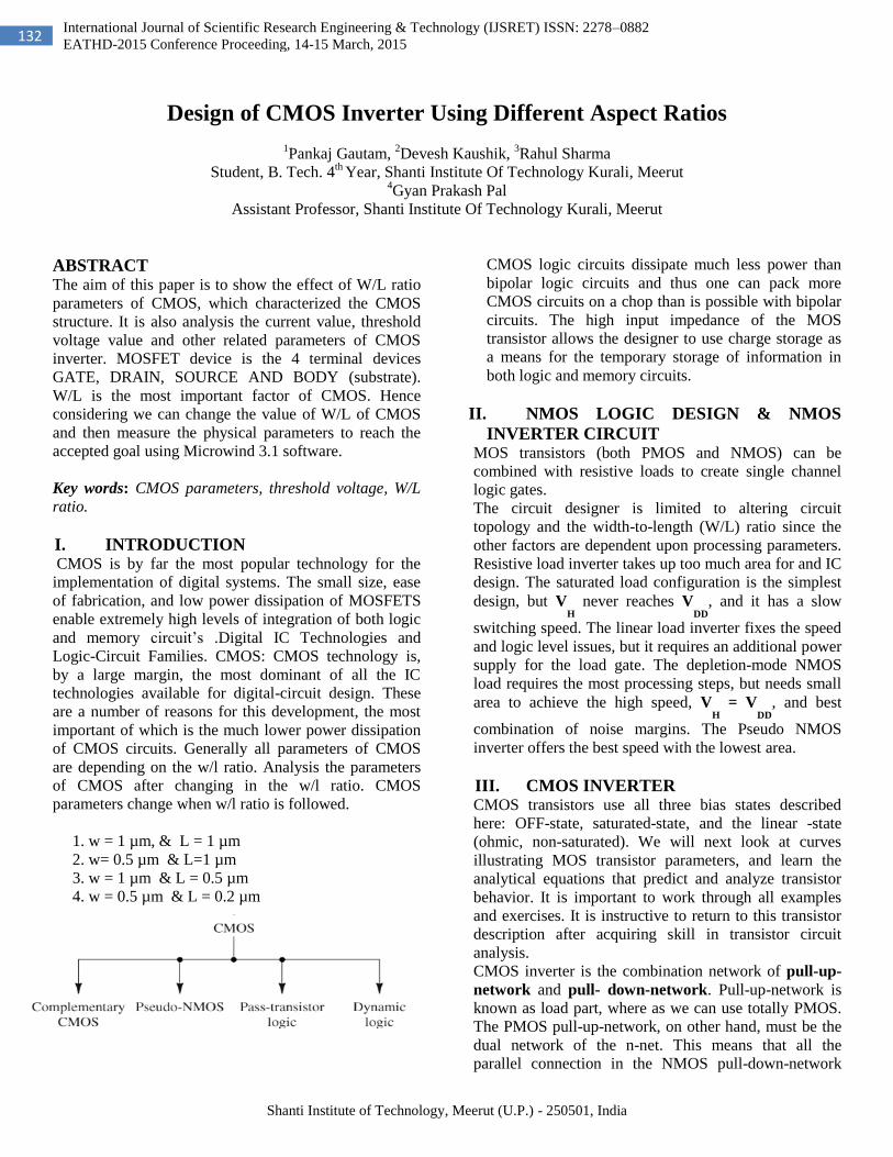
Shanti Institute of Technology, Meerut (U.P.) - 250501, India 132 International Journal of Scientific Research Engineering & Technology (IJSRET) ISSN: 2278 –0882 EATHD-2015 Conference Proceeding, 14-15 March, 2015 Design of CMOS Inverter Using Different Aspect Ratios 1 Pankaj Gautam, 2 Devesh Kaushik, 3 Rahul Sharma Student, B. Tech. 4 th Year, Shanti Institute Of Technology Kurali, Meerut 4 Gyan Prakash Pal Assistant Professor, Shanti Institute Of Technology Kurali, Meerut ABSTRACT The aim of this paper is to show the effect of W/L ratio parameters of CMOS, which characterized the CMOS structure. It is also analysis the current value, threshold voltage value and other related parameters of CMOS inverter. MOSFET device is the 4 terminal devices GATE, DRAIN, SOURCE AND BODY (substrate). W/L is the most important factor of CMOS. Hence considering we can change the value of W/L of CMOS and then measure the physical parameters to reach the accepted goal using Microwind 3.1 software. Key words: CMOS parameters, threshold voltage, W/L ratio. I. INTRODUCTION CMOS is by far the most popular technology for the implementation of digital systems. The small size, ease of fabrication, and low power dissipation of MOSFETS enable extremely high levels of integration of both logic and memory circuit’s .Digital IC Technologies and Logic-Circuit Families. CMOS: CMOS technology is, by a large margin, the most dominant of all the IC technologies available for digital-circuit design. These are a number of reasons for this development, the most important of which is the much lower power dissipation of CMOS circuits. Generally all parameters of CMOS are depending on the w/l ratio. Analysis the parameters of CMOS after changing in the w/l ratio. CMOS parameters change when w/l ratio is followed. 1. w = 1 μm, & L = 1 μm 2. w= 0.5 μm & L=1 μm 3. w = 1 μm & L = 0.5 μm 4. w = 0.5 μm & L = 0.2 μm CMOS logic circuits dissipate much less power than bipolar logic circuits and thus one can pack more CMOS circuits on a chop than is possible with bipolar circuits. The high input impedance of the MOS transistor allows the designer to use charge storage as a means for the temporary storage of information in both logic and memory circuits. II. NMOS LOGIC DESIGN & NMOS INVERTER CIRCUIT MOS transistors (both PMOS and NMOS) can be combined with resistive loads to create single channel logic gates. The circuit designer is limited to altering circuit topology and the width-to-length (W/L) ratio since the other factors are dependent upon processing parameters. Resistive load inverter takes up too much area for and IC design. The saturated load configuration is the simplest design, but V H never reaches V DD , and it has a slow switching speed. The linear load inverter fixes the speed and logic level issues, but it requires an additional power supply for the load gate. The depletion-mode NMOS load requires the most processing steps, but needs small area to achieve the high speed, V H = V DD , and best combination of noise margins. The Pseudo NMOS inverter offers the best speed with the lowest area. III. CMOS INVERTER CMOS transistors use all three bias states described here: OFF-state, saturated-state, and the linear -state (ohmic, non-saturated). We will next look at curves illustrating MOS transistor parameters, and learn the analytical equations that predict and analyze transistor behavior. It is important to work through all examples and exercises. It is instructive to return to this transistor description after acquiring skill in transistor circuit analysis. CMOS inverter is the combination network of pull-up- network and pull- down-network. Pull-up-network is known as load part, where as we can use totally PMOS. The PMOS pull-up-network, on other hand, must be the dual network of the n-net. This means that all the parallel connection in the NMOS pull-down-network
Transcript
Shanti Institute of Technology, Meerut (U.P.) - 250501, India
132 International Journal of Scientific Research Engineering & Technology (IJSRET) ISSN: 2278–0882