Design of Digital Signal Processor N.KARTHIKEYAN, EE12S008 Objective: To design a Digital Signal Processor with reference processor as TMS320C25 in Verilog. TMS320C25 is a 16 bit fixed point digital signal processor. TMS320C25 has on-chip RAM of 544 words (16 bit word), Program memory of 4K words. The TMS320 family optimizes speed by implementing functions in hardware that other processors implement through software or microcode. TMS320C25 is capable of executing 10 million instructions per second. It has 8 auxiliary registers, 8 level hardware stack and a bit-reversed indexing mode. In this project, a digital signal based on TMS320C25 processor, with some modifications are implemented. Our Digital signal processor does not implement some features of TMS320C25 for simplification of the problem such as Serial port, On-chip timer, Synchronization input for synchronous multiprocessor configurations, and Global data memory interface. Architecture: This DSP processor implements Harvard-type architecture that maximizes the processing power by maintaining two separate buses program and data which allows accessing both memories simultaneously for speed execution. Also, one of the advantages in TMS320C25 is that a block of memory can be configured as either program memory or data memory. This allows more flexibility in programming this DSP Processor. On-chip Memory: The program memory has on-chip memory of 4K words (4096x16). Data memory has RAM blocks B0, B1 and B2 with 256, 256, 32 words of memory respectively. While the Processor access the on-chip memory, processor does not need wait states since on-chip memory is fast. In this processor, the external memory access in not considered. The RAM block B0 can be configured as program memory using CNFP instruction and configured as Data memory using CNFD instruction. Whenever it is configured as program memory, it cannot be accessed from Data bus and vice versa. The memory is address using direct addressing (Instruction LSB 7-bits and Data page Pointer 9-bits) and indirect addressing using Auxiliary registers. Up to eight levels of hardware stack are provided for saving the contents of the program counter during interrupts and subroutine calls. Arithmetic and Logic Unit: The processor has 32-bit ALU and 32-bit accumulator. The ALU can perform 32 bit 2’s complement arithmetic operations, with one operand as 32-bit accumulator and other operand may be from T register, P register or Data memory. The result of the ALU operation is always stored in the accumulator. The 32-bit accumulator is split into two 16-bit registers (ACC high and ACC low).
Transcript
Design of Digital Signal Processor
N.KARTHIKEYAN, EE12S008
Objective:
To design a Digital Signal Processor with reference processor as TMS320C25 in Verilog.
TMS320C25 is a 16 bit fixed point digital signal processor. TMS320C25 has on-chip RAM of 544 words
(16 bit word), Program memory of 4K words. The TMS320 family optimizes speed by implementing
functions in hardware that other processors implement through software or microcode. TMS320C25 is
capable of executing 10 million instructions per second. It has 8 auxiliary registers, 8 level hardware
stack and a bit-reversed indexing mode.
In this project, a digital signal based on TMS320C25 processor, with some modifications are
implemented. Our Digital signal processor does not implement some features of TMS320C25 for
simplification of the problem such as Serial port, On-chip timer, Synchronization input for synchronous
multiprocessor configurations, and Global data memory interface.
Architecture:
This DSP processor implements Harvard-type architecture that maximizes the processing power by
maintaining two separate buses program and data which allows accessing both memories
simultaneously for speed execution. Also, one of the advantages in TMS320C25 is that a block of
memory can be configured as either program memory or data memory. This allows more flexibility in
programming this DSP Processor.
On-chip Memory:
The program memory has on-chip memory of 4K words (4096x16). Data memory has RAM blocks B0, B1
and B2 with 256, 256, 32 words of memory respectively. While the Processor access the on-chip
memory, processor does not need wait states since on-chip memory is fast. In this processor, the
external memory access in not considered. The RAM block B0 can be configured as program memory
using CNFP instruction and configured as Data memory using CNFD instruction. Whenever it is
configured as program memory, it cannot be accessed from Data bus and vice versa.
The memory is address using direct addressing (Instruction LSB 7-bits and Data page Pointer 9-bits) and
indirect addressing using Auxiliary registers. Up to eight levels of hardware stack are provided for saving
the contents of the program counter during interrupts and subroutine calls.
Arithmetic and Logic Unit:
The processor has 32-bit ALU and 32-bit accumulator. The ALU can perform 32 bit 2’s complement
arithmetic operations, with one operand as 32-bit accumulator and other operand may be from T
register, P register or Data memory. The result of the ALU operation is always stored in the
accumulator. The 32-bit accumulator is split into two 16-bit registers (ACC high and ACC low).
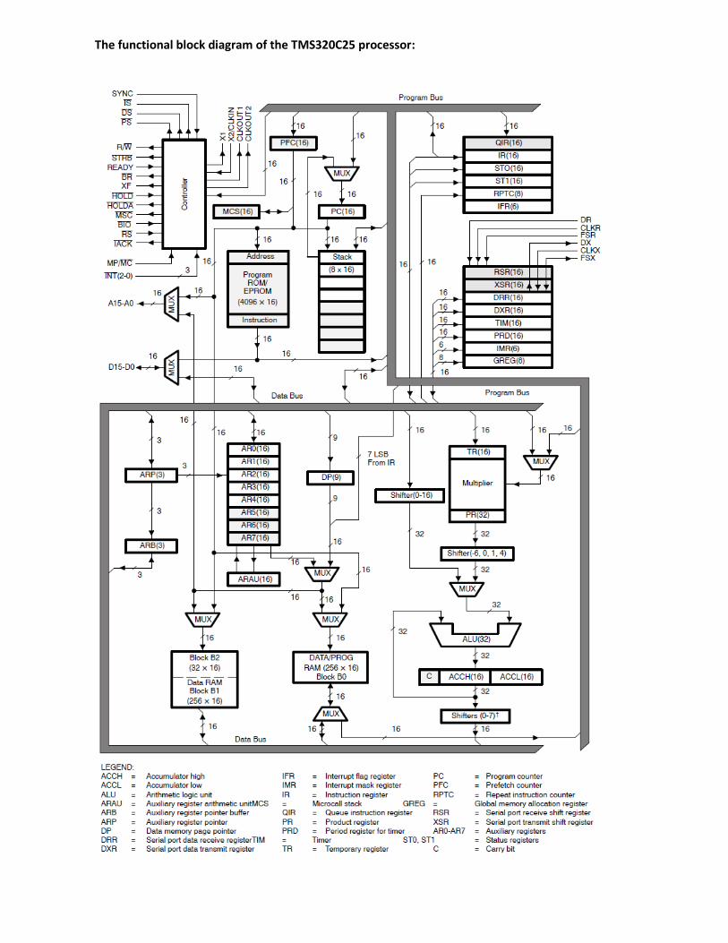
The functional block diagram of the TMS320C25 processor:
Multiplier:
A dedicated hardware multiplier is capable of multiplying two 16-bit signed numbers. The numbers can
be in 2’s complement form and the one of the operands is stored in T register. The other operand can be
taken from either program memory or Data bus. The result of the product is stored in 32-bit PR product
register. With multiply and accumulate instructions, the fast on-chip multiplier allows the device to
perform efficiently the fundamental DSP operations such as convolution, correlation, and filtering.
Shifters:
Apart from the shifter inside ALU, this processor has 3 different shifters. One of the shifter is next to 32-
bit PR product register in order to shift left the multiplied result by (-6,0,1,4) bits. Another Shifter is
between Data bus and the ALU. This shifter shifts the data from data memory before it is taken as 32-bit
operand to ALU. This shifter can shift the data left in range (0 to 16). There is one more shifter after ALU
which shifts the 16 bit data from ACC high or ACC low before stored into the data memory.
Auxiliary Registers Unit:
The processor contains 8 auxiliary registers of 16 bit width. These registers are indexed using ARP
(Auxiliary Register pointer). This unit has a dedicated Arithmetic unit capable of doing Addition,
Subtraction, increment, decrement and reverse carry propagated Addition. The reverse carry
propagation is very useful for bit reverse addressing which is needed for FFT algorithms.
Instruction Set:
TMS320C25 has following types of instructions.
Accumulator and Memory reference instructions,
Auxiliary Registers and Data Page pointer instructions.
T register, P register, and Multiply instructions
Branch/Call instructions
I/O and data memory operations
Control instructions
Out of above types of instructions, the I/O and data memory operations are not implemented in our DSP
processor. The Arithmetic instruction has all the necessary functions such as Addition, Subtraction,
Logical operations, for both in unsigned and signed mode with direct and indirect memory addressing.
Status Register ST0 and ST1 provide a great deal of control flow using various control & Branch
instructions. Multiply and Accumulate instructions such as MAC, MACD, MPYA, SQRA, SQRS, provide
improved flexibility and speed for Digital filter applications.
References:
1) TMS320C2x User Guide(SPRU014C), Texas instruments, October 1992.
2) TMS320C25 Digital signal processor Datasheet.
3) ”Implementation of Texas Instruments TMS32010 DSP Processor on Altera FPGA,” GSPx 2004,
Santa Clara, CA, September 27-30, 2004.
4) John P. Hayes, “Computer Architecture and Organization”, Third Edition, 1998
Design of Simple DSP Processor
DSP Architectures and Embedded systems
Karthikeyan.N EE12S008
EE5030 1
TMS320C25
• 16-bit fixed point DSP core
• Single-cycle multiply/accumulate instructions
• on-chip RAM blocks (Program, Data)
• eight auxiliary registers with a dedicated arithmetic unit
• 80 ns Instruction Cycle time
• Interrupts, serial IO, Hardware Timer, Multi-Processor Support (Not Implemented)
EE5030 2
DSP Architecture
EE5030 3
Central Arithmetic-Logic Unit • 16-bit parallel shifter • 32-bit arithmetic and logical
operations • 16 x 16 bit parallel multiplier
with a 32-bit product • 32-bit accumulator with output
shifter • Single-cycle Multiply-and-
Accumulate instructions
CALU
EE5030 4
ARAU • 8 16-bit registers for indirect addressing or temporary data storage • 16-bit Auxiliary Register Arithmetic Unit including operations with
reversed-carry propagation • ARB during interrupt & function calls
EE5030 5
Memory Addressing
Indirect addressing mode both Address calculation and CALU Operation can be done in parallel. Increment, Decrement • Addition/Subtraction • Reverse Carry
Addition/Subtraction • Change ARP
Direct Addressing Data Address (16 bits) = DP(9 bits) + 7 LSBs of IR