103
Design of High Performance SRAM Based Memory Chip Department of Electronics and communication Engineering National Institute of Technology Rourkela Rourkela, Odisha, 769008, India May 2015

Design of High Performance SRAM Based Memory Chip
Department of Electronics and communication Engineering
National Institute of Technology Rourkela
Rourkela, Odisha, 769008, India
May 2015

Design of High Performance SRAM Based Memory Chip
A thesis submitted in partial fulfillment of the requirement for the degree of
Master of Technology
In
Electronics and Communication
Specialization: VLSI Design & Embedded System
By
SARIKA ANIL KUMAR Roll No. 213EC2193
Under the Supervision of
Prof. Debiprasad Priyabrata Acharya
Department of Electronics and communication Engineering
National Institute of Technology, Rourkela
Rourkela, Odisha, 769008, India
May 2015

DECLARATION
I certify that,
a. The work presented in this paper is an original content of the research
done by myself under the general supervision of my supervisor.
b. The work has not been submitted to any other institute for any degree or
diploma.
c. The data used in this work is taken from free source and its credit has
been cited in reference.
d. The materials (data, theoretical analysis and text) used for this work has
been given credit by citing them in the text of thesis and their details in
the references.
e. I have followed the thesis guidelines provided by the institution
SARIKA ANIL KUMAR
DEPARTMENT OF ELECRTONICS AND COMMUNICATION ENGINEERING
NATIONAL INSTITUTE OF TECHNOLOGY,
ROURKELA, ODISHA -769008.

Dedicated to
My beloved family
And
My dear friends

CERTIFICATE
Place:
Date: Dept. Of Electronics and Communication Engg.
National Institute of Technology
Rourkela-769008
Prof. D. P. Acharya
This is to certify that the work done in the report entitled ―Design of High
Performance SRAM Based Memory Chip” by ―SARIKA ANIL KUMAR” is a
record of research work carried out by him in National Institute of Technology,
Rourkela under my supervision and guidance during 2014-15 in partial fulfillment of
the requirement for the award of degree in Master of Technology in Electronics and
Communication Engineering (VLSI & Embedded Systems), National Institute of
Technology, Rourkela. To the best of my knowledge, this thesis has not been submitted
for any degree or diploma.
DEPARTMENT OF ELECRTONICS AND COMMUNICATIO ENGINEERING,
NATIONAL INSTITUTE OF TECHNOLOGY,
ROURKELA, ODISHA -769008.

1
ACKNOWLEDGEMENT
This research work is one of the significant achievements in my life and is made
possible because of the unending encouragement and motivation given by so many in every
part of my life. It is immense pleasure to have this opportunity to express my gratitude and
regards to them.
Firstly, I would like to express my gratitude and sincere thanks to Prof. D. P.
Acharya, my supervisor, Department of Electronics and Communication Engineering for his
esteemed supervision and guidance during the tenure of my project work. His valuable
advices have motivated me a lot when I feel saturated in my work. His impartial feedback in
every walk of the research has made me to approach a right way in excelling the work. It
would also like to thank him for providing best facilities in the department.
Also, I would like to express my gratitude and respect to Prof. K. K. Mahapatra, Prof.
S. K. Patra, Prof. S. Meher, Prof. A. K. Swain, Prof. M. N. Islam and Prof. P. K. Tiwari for
their support, feedback and guidance throughout my M. Tech course duration. I would also
like to thank all the faculty and staff of the ECE department, NIT Rourkela for their support
and help during the two years of my student life in the department.
Lastly, I am very thankful to all my classmates and seniors of VLSI lab, especially
Mr. Tom, Mr. Soubhagya, Mr. Debasish Nayak, Mr. Umakanta Nanda and all my friends
who always encouraged me in the Successful completion of my thesis work. I would like to
express my love and heartfelt respect to my parents, and friends for their consistent support,
encouragement in every walk of my life without whom I would be nothing.
SARIKA ANIL KUMAR

2
ABSTRACT
The semiconductor memory, SRAM uses a bi-stable latch circuit to store the logic
data 1 or 0. It differs from Dynamic RAM (DRAM) which needs periodic refreshment
operation for the storage of logic data. Depending upon the frequency of operation SRAM
power consumption varies, i.e. it consumes very high power at higher frequencies like
DRAM. The Cache memory present in the microprocessor needs high speed memory, hence
SRAM can be used for that purpose in microprocessors. The DRAM is normally used in the
Main memory of processors, where importance is given to the density than its speed. The
SRAM is also used in industrial subsystems, scientific and automotive electronics.
In this thesis 16-Kb Memory is designed by using the memory banking method in
UMC 90nm technology, which operates at a frequency of 1GHz.The post layout simulation
for the complete design is performed and also obtained power analysis for the overall design.
All peripherals like pre-charge, Row Decoder, Word line driver, Sense amplifier, Column
Decoder/MUX and write driver are designed and layouts of all the above peripherals also
drawn in an optimized manner such that their layout occupies the minimum area. The 6T
SRAM cell is designed with operating frequency of 8 GHz and stability analysis are also
performed for single SRAM cell. The layout of the Single SRAM cell is drawn in a
symmetric manner, such that two adjacent cells can share same contact, which results
reduction in the area of cell layout. The Static Noise Margin, Read noise margin and Write
Noise Margin of single cells are found to be 240mV, 115mV and 425mV respectively, for a
supply voltage of 1V.The effect of the pull-up ratio and cell ratio on the stability of SRAM
cell is observed.

3
Contents
ABSTRACT ................................................................................................................................................ 2
List of Figures: ......................................................................................................................................... 4
List of tables: ........................................................................................................................................... 6
List Of Symblos And Abbreviations ......................................................................................................... 7
1. OVERVIEW ....................................................................................................................................... 8
1.1. Introduction: ........................................................................................................................... 9
1.2. Motivation ............................................................................................................................... 9
1.3. Literature Review: ................................................................................................................. 10
1.4. Thesis organization: .............................................................................................................. 11
2. Brief Review on SRAM Based Memories ...................................................................................... 12
2.1. Review on different SRAM architectures: ............................................................................. 13
2.2. Analysis on SRAM based Memory: ....................................................................................... 30
2.3. Applications of SRAM based memories: ............................................................................... 35
1. SRAM and Its Peripherals .............................................................................................................. 37
1.1. Introduction To SRAM Based Memory: ................................................................................ 39
1.2. Peripheral circuitry of SRAM Based Memory: ...................................................................... 41
2. SRAM Design & Operation ............................................................................................................ 46
2.1. 6T CMOS SRAM CELL: ............................................................................................................ 48
2.2. Stability Analysis of 6T- SRAM Cell: ....................................................................................... 54
3. Memory Banking ........................................................................................................................... 62
3.1. Design of 1Kb memory: ......................................................................................................... 66
3.2. Design of 4Kb Memory Bank: ................................................................................................ 82
3.3. Design of 16-Kb Memory: ..................................................................................................... 85
4. Conclusion and Future Scope ........................................................................................................ 87
4.1. Conclusion: ............................................................................................................................ 88
4.2. Future Scope: ........................................................................................................................ 89
Bibliography .......................................................................................................................................... 90

4
List of Figures: Fig 3.1 Memory Organization of Microprocessor[25] .......................................................................... 39
Fig 3.2 Monolithic Peripheral circuitry of 1Kb SRAM Based Memory [2] ............................................. 41
Fig.4.1 Basic SRAM Memory Cell[1] ...................................................................................................... 47
Fig.4.2 6-Transistor SRAM Memory cell[1] ........................................................................................... 48
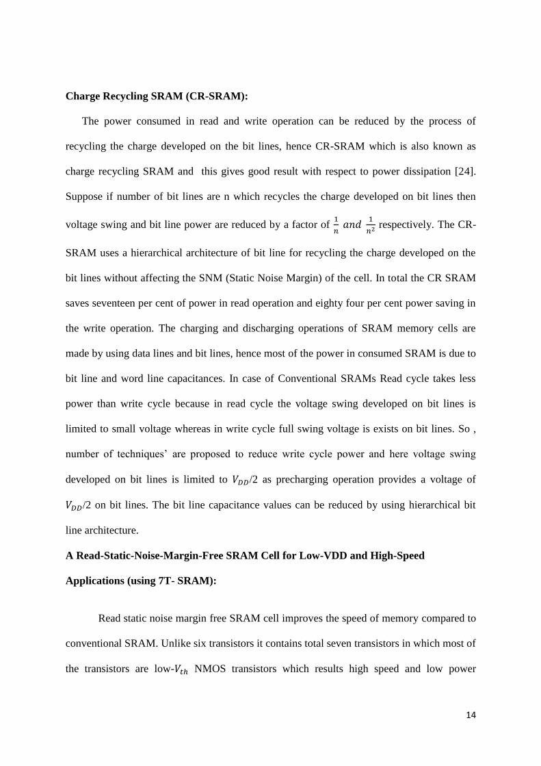
Fig.4.3 Write 0 Operation of 6T cell[1][2] ............................................................................................. 50
Fig.4.4 Read 0 operation of 6T cell[1][2] ............................................................................................... 50
Fig.4.5 Schematic of 6T- SRAM Cell ...................................................................................................... 52
Fig.4.6 symmetric Layout of 6T- SRAM Cell .......................................................................................... 52
Fig.4.7 Simulation results of 6T SRAM Cell ........................................................................................... 53
Fig.4.8 static noise margin representation of 6T-cell ........................................................................... 55
Fig 5.1 DWL (Divide Word Line architecture)[7] ................................................................................... 65
Fig 5.2 16Kb memory using banking method ....................................................................................... 66
Fig 5.3 Pre-charge schematic Fig 5.4 Pre-charge with 32 instances ......................................... 67
Fig 5.5 Pre-charge layout ...................................................................................................................... 67
Fig 5.6 Pre-charge layout of 32 instances ............................................................................................. 68
Fig5.7 schematic of 2to4 NOR Based Decoder ..................................................................................... 68
Fig.5.8 Layout of 2to4 NOR Based Decoder .......................................................................................... 69
Fig.5.9 Av-Extracted view of 2to4 NOR Based Decoder ........................................................................ 69
Fig.5.10 Schematic of 5to32 Decoder ................................................................................................... 70
Fig.5.11 Layout of 5to32 Decoder ......................................................................................................... 71
Fig.5.12 Schematic of Word line Driver ................................................................................................ 72
Fig.5.13 Layout of Word line Driver ...................................................................................................... 72

5
Fig 5.15 Layout of word line driver (32 instances) ................................................................................ 73
Fig5.14 schematic of word line driver (32 instances) ........................................................................... 73
Fig.5.16 Schematic of Sense Amplifier .................................................................................................. 74
Fig.5.17 Layout of Sense Amplifier........................................................................................................ 74
Fig.5.18 Sense Amplifier (8 instances) .................................................................................................. 75
Fig.5.19 Layout of Sense Amplifier (8 instances) .................................................................................. 75
Fig.5.20 Schematic of Write Driver ....................................................................................................... 76
Fig.5.21 Layout of Write Driver ............................................................................................................. 76
Fig.5.22 Write Driver (8 instances) ....................................................................................................... 77
Fig.5.23 Layout of Write Driver (8 instances) ....................................................................................... 77
Fig.5.24 Av- Extracted view of Write Driver (8 instances) .................................................................... 77
Fig.5.25 Schematic of Column Decoder/Mux ....................................................................................... 78
Fig.5.26 Layout of Column Decoder/Mux ............................................................................................. 78
Fig.5.27 Column Decoder/Mux (8 instances) ........................................................................................ 79
Fig.5.28 Layout of Column Decoder/Mux (8 instances) ........................................................................ 79
Fig.5.29 Av-Extracted View of Column Decoder/Mux (8 instances) ..................................................... 79
Fig.5.30 Schematic of 1Kb memory ...................................................................................................... 80
Fig.5.31 Layout of 1Kb memory ............................................................................................................ 80
Fig.5.32 Simulation Results of 1Kb memory ......................................................................................... 81
Fig 5.33 Schematic of 4Kb Memory Bank ............................................................................................. 82
Fig 5.34 Schematic of Bank Multiplexer of 4-Kb Memory .................................................................... 82
Fig 5.35 Layout of Bank Multiplexer of 4Kb Memory Bank .................................................................. 83
Fig 5.36 Layout of 4Kb Memory Bank ................................................................................................... 83
Fig 5.37 Av-Extracted View of 4Kb Memory Bank ................................................................................ 83
Fig 5.38 Simulation Results of 4Kb Memory Bank ................................................................................ 84
Fig 5.39 Schematic of 16-Kb Memory ................................................................................................... 85

6
Fig 5.40 Layout of 16Kb Memory .......................................................................................................... 85
Fig 5.41 Av-Extracted View of 16-Kb Memory ...................................................................................... 86
Fig 5.41simulation results of 16kb SRAM Memory ............................................................................... 86
List of tables:
Table 4.1 Comparison of Power analysis of single SRAM Cell .............................................................. 54
Table4.2 Cell Ratio vs. SNM .................................................................................................................. 56
Table4.3 Pull-up Ratio vs. SNM ............................................................................................................. 56
Table4.4 Read noise Margin vs. Cell Ratio ............................................................................................ 57
Table4.5 Write Noise Margin vs. pull-up ratio ...................................................................................... 59
Table 4.6 Process Corner Analysis ........................................................................................................ 60
Table 4.7 Temperature Analysis............................................................................................................ 60
Table 4.8 Variation of Power with Supply Voltage ............................................................................... 61
Table 5.1 Power Analysis of 1Kb memory............................................................................................. 81
Table 5.2 Power Analysis of 4Kb Memory Bank ................................................................................... 84

7
List Of Symblos And Abbreviations
The following are the list of abbreviations that are used in this thesis.
ASIC Application Specific and Integrated Circuits
CAD Computer Aided Design
CMOS Complementary Metal Oxide Semiconductor
CPL Complementary Pass Transistor Logic
DDR Dual Data Rate
DRAM Dynamic Random Access Memory
DVS Dynamic Voltage Scaling
EEPROM Electrically Erasable PROM
ESD Electro Static Discharge
FPGA Field Programmable Gate Array
FRAM Ferroelectric Random Access Memory
MOSFET Metal Oxide Semiconductor Field Effect Transistor
NVRWM Non Volatile Read Write Memory
PROM Programmable Read Only Memory
QDR Quad Data Rate
RAM Random Access Memory
ROM Read Only Memory
SDRAM Synchronous DRAM
SRAM Static Random Access Memory
TFT Thin Film Transistors
VHDL VHSIC Hardware Description language

8
1. OVERVIEW

9
1.1. Introduction:
Now a day, low power and high speed SRAMs have turned into a discriminating part of
numerous VLSI chips. This is particularly valid for microchips, where the on-chip reserve
sizes are developing with every era to extend the expanding disparity in the speeds of the
processor and the Cache memory [25]. SRAM is utilized as Cache memory which is quick
and used to accelerate the assignment of processor and memory interface. With the new
technologies in VLSI innovation, the speed of the logic gates has expanded essence, but
comparing the memory speed is not enhanced [24]. Thus, for high speed PCs SRAM
memories are critical to enhance operating speed and DRAM are utilized as a part of Main
Memory where Density has more significance than Speed. In this work we have focused on
the outline of high performance 6T SRAM which can be utilized as high speed and low
power memory for PCs.
1.2. Motivation
Present day’s Cache memory sizes are expanded with advancements and they play an
important role in the microchips and System-On-Chip usage. Intel chip family shows that the
on chip cache memory sizes in processor is expanding to increase in speed of memory, with
chip L3 cache size in ―Intel Pentium Clarkdale (32nm) processor ― are increased from 3MB
to 4MB in ―Core-i3 Clarkdale (32nm)‖ to 8MB in ―Core- i5 Lynnfield (45nm) ‖ to 12MB in
―Core-i7 Gulf town (32nm)‖ processor. Similarly Qualcomm Snapdragon S1 processor CPU
L2 Cache size is increased from 256KB to 384KB in Snapdragon S2 to 512KB in
Snapdragon S3 to 1MB with 1.5GHZ in 28nm Technology in Snapdragon S4 processor. [25]

10
With every era, the sizes of cache memory are increasing. The design of such a bigger
memory with high speed and low power consumption is very difficult which has motivated
me a lot towards the design of SRAM Based memory.
1.3. Literature Review:
Debasis Mukherjee, Hemanta Kr. Mondal explained the butterfly method to calculate
static noise margin, write noise margin and read noise margin of a 6T SRAM cell. In
this paper, he explained how the stability of memory cell depends on the values of
the pull up ratio and cell ratio [3].
Jan M. Rabaey Anantha Chandrakasan Borivoje Nikolic [2] explained the design of
SRAM Based memory with all peripherals like pre-charge, row decoder, sense
amplifier, tree decoder for column multiplexing. Monolithic architecture for small
memory design is explained in a clear manner.
Sung-Mo Kang and Yusuf Leblebici explained the design of the single 6T SRAM
such that during read operation it should not allow modification for the stored data
and during write operation it should allow modification of the stored data. [1]
Kunihiko Yamaguchi, Hiroaki Nambu et al. [14] has developed 64Kb ECL CMOS
SRAM based memory. In this thesis he utilizes a blend of ECL word line drivers and
CMOS SRAM cell arrays and some write circuits. Without any intermediate voltage
level converter the ECL word line drivers and write circuit drives the CMOS SRAM
Cell arrays.
Dr. Robert H. Dennard, in 1966, made the one transistor DRAM. He utilized a
solitary transistor and a capacitor to make an easier memory cell. Dr. Dennard with
IBM conceded a patent for DRAM in 1968. Fairchild Corporation grew initial 256-k
SRAM contribute 1970 [9].

11
Katsuro Sasaki, a proposed novel building design that empowers quick write and read
in Poly type PMOS load (or) high poly resistive load with only single bit line in a
memory cell. By using bit line pulsing technique the architecture uses an alternate
twin word activation (ATWA) for efficient write operation [12].
Rakesh Chandankhede, has proposed a decoupled latch with a current controlled
sense amplifier which gives improvement in power consumption and performance. At
the point when EN sign is low, the logic on BT and BB grows on the latch output, i.e.
differential voltage, however, it is not getting increased as the pull down transistor is
off and consequently same logic holds still EN goes high. Here line having low
voltage goes to release to ground when EN signal goes high [13].
Sreerama Reddy G. M, P Chandrasekhara Reddy designed 8 KB Low Power SRAM
in 180nm Technology using the memory banking method which operates at 800 MHz.
In this thesis he explained the reduction in power dissipation and clock delay [15]
1.4. Thesis organization:
This thesis will explain the high performance SRAM Based memory design using the
Memory banking method. The Introduction and motivation of the thesis are explained in
chapter1.Chapter 2 desribes the brief survey of SRAM based memories. Chapter 3 Describes
peripheral Circuitry of the SRAM Based memory. The Design of Single 6T cell and stability
analysis of memory cells is explained in chapter4. Chapter 5 describes the concept of
memory banking and results of the complete design. Finally the conclusion and future scope
are explained in chapter 6.

12
2. Brief Review on SRAM
Based Memories

13
This chapter includes the brief survey on different SRAM architectures,various analysis on
SRAM based memories and finally applications of SRAM memories.
2.1. Review on different SRAM architectures:
SRAM Array Structures for Energy Efficiency Enhancement (number of rows less than
columns using 8T SRAM):
In ultra-low power application design of energy efficient SRAM structures is very important.
In traditional, the SRAM array contains more number of rows than the number of columns,
but here [23] at a particular lower supply voltage, better energy efficiency can be achieved
with a wider SRAM structure where the number of rows are less than the number of columns.
Here we can get an energy improvement of 38% for a 64Kb and 10% for 8kb SRAM array
with same power supply voltage. Minimum energy can be consumed by using a power supply
voltage whose value is equal or lower than the threshold voltage value. But the lower value of
power supply voltage affects the stability of the design, i.e. noise margin is reduced. It can be
observed that minimize energy consumption is achieved in non-square type memory array
structures, whereas minimum access time is achieved in square type memory array structure.
Both dynamic and static energy of word lines and bit lines are affected by power supply
voltage, i.e. energy consumption decreases with decreasing the supply voltage. The
limitations of the 6T SRAM cell are eliminated by 8T cell which uses separate port for
reading operation. The capacitances of word line and bit line decide the value of dynamic
energy, whereas memory density decides the leakage current which is responsible for static
power dissipation. For higher power supply voltages, i.e. above 0.7 V the number of rows is
128 whose number is greater than the number of columns i.e. 64 for an 8Kb memory with
fixed density. Whereas the number of rows is gradually reduced with a power supply ranges
0.3 V to 0.7 V. In the design of 64Kb which consists of total 8 banks and size of each bank
is to be 8Kb the number of rows are reduced to 32 from 128 [23].
14
Charge Recycling SRAM (CR-SRAM):
The power consumed in read and write operation can be reduced by the process of
recycling the charge developed on the bit lines, hence CR-SRAM which is also known as
charge recycling SRAM and this gives good result with respect to power dissipation [24].
Suppose if number of bit lines are n which recycles the charge developed on bit lines then
voltage swing and bit line power are reduced by a factor of
respectively. The CR-
SRAM uses a hierarchical architecture of bit line for recycling the charge developed on the
bit lines without affecting the SNM (Static Noise Margin) of the cell. In total the CR SRAM
saves seventeen per cent of power in read operation and eighty four per cent power saving in
the write operation. The charging and discharging operations of SRAM memory cells are
made by using data lines and bit lines, hence most of the power in consumed SRAM is due to
bit line and word line capacitances. In case of Conventional SRAMs Read cycle takes less
power than write cycle because in read cycle the voltage swing developed on bit lines is
limited to small voltage whereas in write cycle full swing voltage is exists on bit lines. So ,
number of techniques’ are proposed to reduce write cycle power and here voltage swing
developed on bit lines is limited to /2 as precharging operation provides a voltage of
/2 on bit lines. The bit line capacitance values can be reduced by using hierarchical bit
line architecture.
A Read-Static-Noise-Margin-Free SRAM Cell for Low-VDD and High-Speed
Applications (using 7T- SRAM):
Read static noise margin free SRAM cell improves the speed of memory compared to
conventional SRAM. Unlike six transistors it contains total seven transistors in which most of
the transistors are low- NMOS transistors which results high speed and low power

15
dissipation memory. Compared to conventional 6T SRAM the proposed read static noise
margin free 7T-SRAM has less area which is 23% smaller than conventional SRAM [25]. To
reduce the power dissipation in the memory design, Dynamic Voltage Scaling (DVS)
technique is used. With the lower supply voltage, the delays in SRAM increases at a higher
rate compared to the delays of CMOS logic circuits and during read operation, lower supply
voltage results loss of data stored in the memory cell [25]. To find the effect caused by a
transistor mismatch in the memory cell, Monte Carlo Simulations are performed with a
standard deviation of (1/10) of threshold voltage. The values of Read Static Noise Margin
and cell current are highly depending on the driving capability of NMOS access Transistors.
As driving capability of access transistor increases then the value of read static noise margin
decreases whereas cell current increases.
Low-Power SRAM Design with Negative Word-Line Scheme (using 4T- SRAM):
To reduce the leakage current present in the access transistors , a 4T-SRAM is
proposed that uses negative word-line scheme which gives lot of improvement in terms of
power dissipation. As the memory size increases, then the leakage currents also increases
which results more power dissipation even in standby mode. High speed and low power
memory design is very important and this can be achieved by varying the threshold voltage
values of access transistors, which are controlled by the word lines. Low threshold access
transistors are used to speed up the read and write operation of memory cell [26] , whereas
high threshold access transistors are used to reduce the leakage current present in the memory
cell. Unlike conventional 6T SRAM, the 4T SRAM does not contain any load and 4T SRAM
occupies 35% less area compared to conventional SRAM and it consumes 29% less power
dissipation compared to conventional 6T SRAM Memory cell. It is observed that leakage
current in NMOS transistors is greater than the leakage current in PMOS transistors for a
particular reverse voltage of same magnitude. Also we can notice that the p type latch n type

16
access 4T SRAM saves more power compared to n type latch p type access 4T SRAM when
negative word line scheme used .
SRAM Leakage Reduction by Row/Column Redundancy under Random Within-Die
Delay Variation (using conventional 6T SRAM):
The contribution of leakage current in power dissipation is increases with the voltage
scaling in case of SRAM based memories. By increasing the reverse bias voltage at body we
can increase threshold voltage which results reduction in sub threshold current but speed of
memory is reduces because of the above reverse biasing. Hence after reverse biasing at body,
the subsequent delay rises and less number of cells violates the original delay of the SRAM
memory block and these cells are replaced by spare SRAM columns and rows. In the sub 90
nm technologies because of the within-die variations, identical memory cells also shows
different delays in a memory cell array [27]. From the Empirical formulae based studies it is
known that 3.54% of random variation in delay is observed because of within-die variation in
case of 90 nm field programmable gate arrays (FPGAs). These variations can be modelled by
using Gaussian distribution whose results are matched to the results of statistical based
studies. Cache memory leakages can be reduced by switch off the unused parts and put them
in a sleepy mode which is having lower energy and this can be done by using two different
power supply voltages. By using dual threshold voltages and dual oxide thickness values we
can minimize the leakages present in the SRAM Based cache memories. To improve the
yield of memory and to repair fault cells present in a memory, the spare cells which are
nothing but redundant cells are used.
Characterization of a Novel Nine-Transistor SRAM Cell:
In present days high performance integrated circuits are required and these circuits
maximum amount of energy approximately 40% is wasted because of leakage currents. Main
source of this leakage current is designing of SRAM cell in the memory banks. Another

17
important problem in the CMOS technology with the scaling of transistor size is stability of
the data in SRAM cell that may decrease, so this become the major problem in standard 6-T
SRAM cell CMOS technology [30].To overcome these disadvantages 9-T SRAM cell is
proposed instead of using 6-T SRAM cell. The proposed SRAM cell will increase the data
stability by two times and reduces the leakage power by 23% than the standard 6-T SRAM
cell design, by placing the 9-T SRAM cells in super cut off mode. Here two data access
methods will provide for write and read operations. The static noise margin of the read
operation will double by isolating data storage nodes from the bit lines. In the proposed 9-T
SRAM cell the upper 6 transistors are same as standard 6-T SRAM structure; additional 3
transistors will be at the lower sub section of the circuit. Among those 3 transistors 2 will be
composed of bit lines like the upper sub-circuit and the third will one read access transistor.
SRAM Circuit with Expanded Operating Margin and Reduced Stand-By Leakage
Current Using Thin-BOX FD-SOI Transistors:
Because of technology scaling the leakage current is gradually increases whereas
operating margin is decreases. Hence to overcome the above two problems SRAM circuit
with low power design is proposed which uses fully depleted buried oxide silicon on insulator
transistors [31]. By introducing back gate bias at SRAM cell we can achieve high frequency
of operation and high operating margin even at lower power supply voltages. The proposed
structure gives 30% faster writing time and 90% less power dissipation compared to
conventional SRAM Cell. The main reason for reducing operating margin is the mismatch of
threshold voltages between transistors in memory cell. The reduction of power supply voltage
implies a reduction of cell current which leads to the reduction of operating frequency.

18
Low-Power Embedded SRAM with the Current-Mode Write Technique (using
proposed 7T-SRAM Cell):
In conventional current mode type SRAM’s, the write operation is not performed in
current-mode because of power dissipation and only read operation is performed in most of
design technique. In this paper, current-mode technique proposed which is used for both read
operation as well as write operation. Due to the current mode operations voltage swings are
kept very small at bit line as well as in data line during write operation and read operation ,
which results to reduction in power consumption (i.e. ac power dissipation/consumption is
proportional to voltage swing ).This current-mode SRAM has seven building blocks i.e.
Address decoder , equalizer circuit,7-T SRAM memory cell, ntype current conveyor [33],
ptype current conveyor, Data input circuit and finally Clamped type bit line sense amplifier.
In write operation data is written into the bit line by using two access pass transistor, which is
controlled by a enable (WE) signal. When it enabled, the differential current is passed to
write data lines. In this paper a New 7T is proposed, which is having one extra transistor Meq
compared to convention 6T SRAM. The extra transistor is used to clear the data present in
the cell before every write operation .In case of Meq off state, it is working like a
conventional SRAM cell. This proposed new current-mode SRAM is designed on 0.6-um
CMOS technology of 128x8 cell , which consumes only 30% of the power in read operation.
High-Speed Boosted and Offset-Grounded Data Storage (BOGS) SRAM Cell
Architecture:
Boosted and Offset-Grounded Data Storage (BOGS) [34]minimizes the amount of
charge required to boost up the effective gate to source voltage (VGS - VT ) which is supplied
from the charge pump circuit. It boosts the effective gate to source voltage up to 0.8v which
is necessary to achieve 100MHZ frequency of operation even at 0.5v of supply voltage. Solar

19
battery operated portable equipment like wrist watch like computer requires an SRAM which
can operate at 0.5v supply voltage with 100MHZ operation capable of doing read or write
operations between the CPU and cache memory. While lowering the SRAM supply voltage
to 0.5v which is offered by a single solar battery, it is necessary to maintain sufficient
effective drain to source voltage by still avoiding the sub-threshold leakage. Reducing VT can
reduce the effective gate to source voltage but this produces a leakage current of 10A for -
0.3V VT while operating at 100MHZ. BOGS use the low power strategy by putting the right
boosted power supply in to the less power consumed transistor of SRAM cell. It uses pulse-
shifting (0.5V/0V- 1.3V/0.65V) of the data storage node pairs of the unselected cell which
frees the charge pump circuits from driving virtual bit line (BL) and select line (SL)
discharging which is resulted by using the ground. Virtual SL driving can increase the
effective gate to source voltage of access and drive transistors up to 0.8V during access time
and during standby mode the virtual SL line with a potential of 0.65V will suppress the
leakage through the access transistor.
ECL-CMOS RAM Macro for SRAM based memory:
In this paper [35], the authors have designed an ultra-high speed SRAM based
memory by incorporating two techniques named ECL-decoder/driver circuit along with a Bi-
CMOS inverter and a pulse generator for write operation with a similar memory cell. Using
these methods they eventually reduced the access-time [13] and the write pulse width by 71
% and 58 % lesser than the conventional SRAM memories. They proposed a twisted bit-line
structure to drive the CMOS memory cells at extremely high speeds. The authors also proved
that the proposed techniques not only hold efficient for ultra-high speed operation but also for
high density.

20
DDR3 SRAM for ultra-fast systems (1.5 Gbps):
In this paper [36] the authors described a 1.5Gbps, 72Mb double-data rate 3(DDR3)
with a supply voltage of 1.2volts .SRAM that account for ultra-fast systems. They fabricated
72-Mb SRAM a 100nm CMOS-technology violating 1 µm2 barrier for the cell size. They
implemented a cell of size 0.845 µm2
which is the smallest one of their times. The proposed
SRAM cell operates in two different user defined modes, namely Clock Aligned (CA) mode
and the other mode which is known as Clock Centred (CC) mode. They proposed a clock
adjustment circuit that provides a phase shift of 0 from the external
clock by which sampling of address, control, and input data can be done efficiently [14].
Whereas in CC Mode they generated clocks in synchronous with rising edge and falling edge
of external clock to sample the inputs. They also developed an on-chip termination to
improve signal integrity.
A Novel High Speed, Three Element Si-Based Static Random Access Memory (SRAM)
Cell:
A three element SRAM cell is proposed which has less power consumption and well
defined off state compared to the other existing technologies. This paper [37] proposes a new
bi-stable SiGe-Si diode as a memory element and the other two elements are gate and load.
The diode has layers of p-type followed by untapped Si buffer, followed by super lattice
followed by Ga-Si well followed by layer n-type. Bi-stable diode has two states, if the
forward voltage greater than 0.8v is there, it has less resistance around 6 ohms and if it is in
reverse bias, it has resistance of 20Mohm. The switching speed of the device depends upon
the transit time of the holes crossing buffered layer, the transit time is around 4ps for the
specifications provided in the paper. So this feature helps to move for high speed memory
applications. In this three element SRAM cell TFT transistor is the load and mosfet as the

21
gate. The noise margin of three element SRAM cell is around 2 V which is sufficient. The
proposed device offers both high density and high speed.
A Replica Technique for Word line and Sense Control in Low-Power SRAM’s:
As Technology growth/ Device dimension reduction in VLSI, fluctuations in
threshold voltage and supply voltage will begin which results serious impacts on the
operating frequency as well as power consumption of SRAM memories. This paper [38]
explains various techniques that are presented to reduce the variation of speed and power on
operating conditions. Replica-delay circuit is designed to reduce bit-line voltage swing using
sense clock and control word-line pulse widths. This circuit tries to reduce the variations in
the operating frequency and power of the memory cell by varying functional conditions and
is exclusively suitable for SRAM’s with large bit-line loads. There are two types of circuits in
which one uses bit-line capacitance type ratioing and other one uses the cell current type
ratioing. In capacitive type ratioing circuit, the replica delay circuit is coupled to a duplicate
bit-line whose capacitance value is a fraction of main bit-line capacitance . For proper
sensing operation the fraction value is decided by the required bit line voltage swing. But in
the cell-ratioing circuit, in order to get local resetting an extra column as well as an extra row
comprising replica memory cells to be used.
CMOS SRAM with high speed decoder using SCL circuits, a sense amplifier with
NMOS source followers, and a sense-amplifier activation-pulse generator with
duplicated SRAM array:
In this paper [39] the proposed device has decoder, memory cell array, pulse
generator for sense amplifier activation and sense amplifier. The proposed device developed
with 0.25um CMOS technology with1.8ns clock access time. This device has three main key
techniques to improve the speed, first one is by combining source coupled logic (SCL)
circuits with reset circuits and the second one is by using NMOS source followers in sense

22
amplifiers, so that there is a large reduction in power dissipation and the third technique uses
duplicate memory in sense amplifier activation pulse generators. In high density SRAM
memory, delay is more due to the large capacitance of large memory, so to reduce this delay
[39], source coupled logic gates are used, which reduces the time delay between decoder and
sense amplifier. The n-type source followers are used in the sense amplifier, which reduces
the time margin between sense amplifier and output from the memory. The delay time
decreased by 9% and activation current decreases by 14% in the proposed device compared
to the conventional device. These circuit techniques provide high speed and high density
SRAM’s with improved performance.
Adaptive Body Bias for Reducing the Impacts of NBTI and Process Variations on 6T
SRAM Cells:
Major challenges in the submicron technologies that SRAM designers facing are
variability and reliability. To expand the consistency and yield of SRAM cell for
compensating Negative Bias Temperature Instability (NBTI) aging and process-variations,
Adaptive Body Bias (ABB) circuit is proposed with low area overhead [42]. This ABB
circuit contains an on-chip analog controller and a threshold voltage sensing circuit. There are
many factors that will have great impact on SRAM reliability. Those factors include circuits
with high density, speedy circuits, power supplies with low value and shrinking geometries.
Generation of interface traps at negative voltages for a particular temperature is called NBTI.
Another parameter in SRAM design is yield. This low yield is because of the failure of
memory functionality which is caused by process variations. This process variation mainly
depends on device sizes. Generally, forward -body bias (FBB) decreases and reverse-
body bias (RBB) increases the . Adaptive Body Bias compensates the effects of NBTI and
process variations by tuning the threshold voltage , which can be done by controlling body
to source voltage of the transistor.

23
Power Reduction Techniques for ECL-CMOS SRAM:
When designing an integrated circuit using SRAM cells, we have to take care of
power dissipation in the circuit. This power dissipation is directly proportional to the
operating frequency of the circuit [43]. So when we are designing the circuit at higher
frequencies, power dissipation is increased. This high speed SRAM cells are used in cache
memory. To reduce the power dissipation in the SRAM design different techniques are
proposed one of them is using bit-line driver, write circuit and the Y decoder. Here bit-line
driver consists of CMOS circuits, write circuit consists of ECL and BICMOS circuits and Y
decoder consists of CMOS and ECL circuits. Here by using variable load impedance type
reduces the power of bit line driver by 96% and the level-shifted Bi-NMOS driver reduces by
56%, so overall the power reduced by 74%.
A Low-Power SRAM Using Hierarchical Bit Line and Local Sense Amplifiers:
Bit line capacitance and bit line write voltage swing can be reduced by using
hierarchical bit line [45] and local sense-amplifier. Without affecting static noise margin it
reduces the bit line power consumption in writing cycle by providing low voltage swing to
the high capacitive bit line and high voltage swing to low capacitive sub bit lines. It reduces
the bit line voltage swing to (
) in both write operation as well as in read operation.
percentage saving in the write power in this structure is 34% compared to conventional
SRAM design. In 250nm technology at an operating frequency of 200MHz with a power
supply voltage of 2.5V, the 8K×32 SRAM chip consumes 26 mw and 28 mw in read and
write operations respectively. Bit line capacitance is the combination of drain capacitance of
access pass transistor and metal capacitance of bit lines and by reducing the capacitance on
bit lines both read power and write power can be minimized.
Heterogeneous SRAM Cell Sizing for Low-Power Applications:

24
Much previous research is generally focused on the reduction of power consumption
in various multimedia applications. But to minimize the consumption of power in the CMOS
VLSI circuits we need to scale the supply voltage, while scaling the supply voltage if it
decreases, causes the SRAM cell failure probability will be increased [46]. To overcome the
increase in SRAM cell failure problems, number of transistors in SRAM structure will be
increased i.e. 8 or 10 numbers of transistors are used in SRAM structures. While doing like
these read stabilities will be increased, but other SRAM cells deteriorate with large area
penalties. In some cases to diminish the area overheads hybrid transistor structures are used.
Here hybrid structures are single ended, in this small number of bit cells are used in a single
line and error correction codes are also used to increase the efficiency which means these
ECC codes decreased the SRAM failure cases. At recent SRAM sizing cases consisted of
embedded memory with H.264 processor, here higher order data bits are occupying a large
SRAM cell and less order data bits are occupying smallest SRAM cells. Hence the failure
cases of SRAM cells will be decreased and attains better video quality under consideration of
area as a control parameter. In general this h.264 processor is one of the heterogeneous
algorithm, one best adequate feature of this algorithm is it is dynamically programmable, it
gives the best results compared with that of brute force search algorithm. Finally it is giving
the better PSNR compared with more other algorithms.
Threshold Voltage Design and Performance Assessment of Hetero-Channel SRAM
Cells:
This paper [47] contains the improved optimum voltage ( ) proposal to enhance the
immunity of super threshold and sub threshold six transistor cell. Static RAM cell is working
at low ( ), and low ( ) shows slighter variability and the trade-off between leakage and
performance has to be considered. Super threshold static RAM operated at very high ( ),
static RAM with high ( ) shows lesser variability by Comparing with the low ( ) design

25
.The hetero channel static RAM support high ( ) design and show better Read/Write
performance and stability it maintain similar RSNM variations for super threshold statis
RAM applications. The devices like hetero channel using third-fifth (or) Germanium material
for forthcoming CMOS technology because of their high electron mobility. For near sub
threshold static RAM cells shows that variability and the stability of static RAM cells
improved by using lower ( ) devives. The variability, stability, cell leakage and performance
of third-fifth and GeOI static RAM cells are investigated in two scenario’s (GEOI (PFET)
and GEOI NFET / InGaAs-OI(NFET) ) .
CMOS SRAM with Offset-Voltage-Insensitive Current Sense Amplifiers
In this paper [48], the authors have designed a 4 Mb CMOS Static RAM in which the
incorporated technology is 0.25 pm. The access-time of address they obtained is 6 ns for a
supply-voltage of 2.7v. The Fast access time is achieved by using a current-sense amplifier
which doesn’t rely upon to offset voltage. They also incorporated a boosted-cell-array
architecture that enables low voltage operation using TFT load-cells. The current sense
amplifier is incorporated with a sensing scheme that enables fast operation by reducing the
access time. They reduced the offset-voltage to 5mv by common centroid geometry to
enhance the sensing operation.
ECL-CMOS SRAM with twisted bit line structure with MOS Equalizer:
ECL-CMOS SRAM circuit technique is used for achieving ultra-high speed which
uses a combination of CMOS cell arrays and ECL word drivers and write circuits [49]. A
twisted bit line structure with MOS equalizer is proposed to reduce the crosstalk noise in
CMOS memory cells. The address access time is the sum of the delays produce by word
decoder or driver circuits, sense circuits and array of memory cell. The delay offered by word

26
decoder/ driver circuits is the largest. In order to increase the speed of operation overall
access time should be reduced which can be reduced by reducing word decoder or driver
circuit delay. To reduce the cycle access time of SRAM it is required to shorten the write
pulse width. It is provided by write-pulse generator circuit with a replica memory cell. Write
pulse is generated by widening the width of the clock pulse using write pulse generator
circuit which consists of delay-gates and OR gate. The write pulse width must be much larger
than write time required to write the data into memory. The pulse width would be the same
as write time of the replica memory cell, thus reducing the pulse width.
High-k Metal Gate SRAM with Adaptive Dynamic Stability Enhancement for Low-
Voltage Operation:
In this paper [50] the authors addressed the issue of density and power benefits that
conventional SRAM is facing due to shrink in SRAM bit cell design-margin. Shrinking is due
to systematic and random process-variations in technology scaling. The scheme they adopted
is adaptive dynamic SRAM word-line under drive (ADWLUD).This scheme incorporates a
bit cell based sensor that improves capability of WLUD of each die. The scheme dynamically
tracks skew-corners of process variations to ensure if of each die is limited by its
write margin. The scheme also tracks P/N shift variation with temperature to check for write
limited dice for stability of read operation is limited. Suppose dice are ensured for no write
limitation then the scheme is applied for read-stability improvement.
SRAM Design with Dynamic Sleep Transistor for Leakage Reduction:
Because of scaling in CMOS technology, there are some advantages and
disadvantages. Main advantages are switching delay with the high density in area. But
because of this scaling leakage current will increase and power will increase. In VLSI
technology there are new challenges because of this miniaturization. These challenges
include process variation instability and transistor leakage is increases. To achieve this

27
scaling mainly SRAM should be scaled. This SRAM mainly depends on process variations
[51]. One of the main drawbacks from scaling is leakage power increases. This leakage
power will contain three types of leakage powers; those are sub-threshold leakage, junction
leakage and gate leakage. This leakage power can be reduced by decreasing the full power
supply. One technique is using the dynamic NMOS sleep transistor for reducing leakage
power. In this method we will control the cell virtual ground through NMOS bias transistors
which can be programmable.
Low power Memristor Based 7T SRAM Using MTCMOS Technique:
Because of scaling in CMOS technologies the demand for devices with low power is
increases and the size of memory chip decreases which in turn increases the transistor count
on the memory chip. Normally number of transistors that are used to store the data are more
compared to number of transistors that actually used to perform any logic function. In this
paper memristor based 7T SRAM [52] is designed which gives better operating frequency
and low power compared to conventional 6T SRAM cell .Memristor is a nonlinear resistor
which is used as a memory to store the data and gives better speed and optimum power
consumption. It improves the performance of memory by reducing leakage currents which
can be achieved by disable the inactive circuit elements. Memristor based SRAM is non-
volatile in nature it saves the data even in the absence power supply. IN 7T SRAM two
memristors are connected between power supply and PMOS of two inverters present in the
memory cell.
A Forward Body-Biased Low-Leakage SRAM Cache:
This papers introduces a new technique to reduce the standby power and active power
by using forward body biasing (FBB) [53].By using super high threshold voltage devices the
leakages in cache can be minimized and dynamically forward body biasing is applied only on

28
specific SRAM cells to improve the speed of operation. Super high threshold voltage devices
can be implemented by using two dimensional halos doping by taking different leakage
mechanisms in Nano technologies. The latency period for transition and energy associated
with forward body biasing can be minimised by activating the memory cells before the read
operation. The proposed structure gives 64% reduction in leakage power and 7.3% of
improvement in bit line delay and it achieves a value of static noise margin which is
comparable to conventional SRAM cell.
Reducing SRAM Power Using Fine-Grained Word line Pulse width Control:
Now a days there is a lot of demand for embedded SRAMs compared to SoC’s and it
requires low power SRAM to achieve a high performance with high packing density .SRAM
cells consumes huge power to achieve correct read operation and to reach required
specifications, in presence of large process variations .here the proposed architecture reduces
the switching power of memory array. This proposed structure combines the delay elements
which are digitally controlled and built in self-test (BIST)[54] to reduce pulse width of word
line for memory design to ensure accurate read operation which results reduction in switching
power. Monte Carlo simulation is performed to analyse the power saving of proposed 1Mb
SRAM macro in 45nm technology. For the proposed architecture with a size of 48Mb, 27%
of power reduction is achieved with yield of 95%.
A Charge-Transfer Amplifier and an Encoded-Bus Architecture for Low-Power
RAM’s:
By using charge transfer pre sense amplifier [55] and encoding method for bus signal
we can achieve a memory design with low power. It reduces the offset voltage between pair
of MOS devices and it overcomes the threshold voltage difference between these MOS
transistors. The bus encoded method reduces the number of signals that are switched to
reduce the capacitive load present at bit lines and to produce low power DLL the dynamic

29
read path contains eight timings. The proposed 2K×16 SRAM memory operates at a
frequency of 50MHz and with a power consumption of 5mwatt at a supply voltage of 1V in
350nm technology.
CMOS SRAM Array With Dynamic Cell Biasing:
In this paper [56], the authors designed an SRAM Array in 65 nm CMOS technology
which can tolerate fluctuations. Technology scaling is limited by fluctuations. Measurement
of local random distributions of node voltages in CMOS SRAM while write, read and
retention operation modes. Using the measurements they noted the insights into dependencies
of terminal voltages. They increased the cell immunity over fluctuations efficiently by
incorporating asymmetry in read write of the terminal voltages of cell dynamically. They
explained these circuit combinations incorporating the dynamic cell-biasing schemes. They
designed PDSOI CMOS SRAM array using a 65nm SRAM which is conventional one. The
proposed technique consumes 10% to 12% in area overhead and achieves 50% reduction in
leakage power.
Statistical SRAM Read Access Yield improvement Using Negative Capacitance
Circuits:
In modern IC designs the SRAM is very important block and occupies more than fifty
per cent of die area. With the technology scaling the process variations are gradually
increases so design of high performance memory is the big challenge for designers [57].This
process variations causes failures in read operation, write operation and static noise margin
analysis. In this proposed design a novel negative capacitive circuits are used to reduce bit
line parasitic capacitances and improves the yield of memory in presence of process
variations. Typically the SRAM cell shows the major sensitivity to various sources of with-
in-die variations i.e. Random –Dopant Fluctuations (RDF) and Line-Edge Roughness (LER).

30
For the proposed design in TSMC 65 nm technology the simulations of 512 SRAM cells
results an improvement of read access yield to 100% from 61.9% .
On-Chip Voltage Down Converter to Improve SRAM Read/Write Margin and Static
Power:
A Bidirectional read and write shared sense amplifier (BSA) [58] acts as a sense
amplifier in reading operations, and acts as a data input buffer and write driver circuit in write
operations. The read and write shared sense amplifier permits the SRAM to ensure 256 I/O’s
and the self-timed pulsed word line structure reduces the power dissipation. An experimental
SRAM is fabricated in a 350 Nano-meter technology with four metal layers and gives an
ultra-high speed embedded memories in processors which operates at 200 MHz frequency. It
is outfitted a wide I/O interface with a constant die-size. It consumes less power because of
the use of the small voltage swing and differential I/O’s. In this proposed design, the metal
four is used for the wide I/O buses placed out directly upon the memory cell arrays. It
removes pipe-line delays and improves operating bandwidth. This design can obtain higher
bandwidth of 9.44Gbps and it can attain very low power of 250mW/G bytes. It gives high
noise immunity and consumes less power.
2.2. Analysis on SRAM based Memory:
Stability Estimation of a 6T-SRAM Cell Using a Nonlinear Regression:
The stability of memory cell is mainly decided by the value of static noise margin.
The cell current present in the memory cell is used to find the stability of cell in read and
write operations. The yield of SRAM based memory is decided by static Noise margin and
write noise margin [59]. The cell currents are measured by varying power supply voltages
which are used to measure the stability of cell design. Read Noise Margin and Write Noise
Margin are two special cases in static noise margin which defines the maximum noise voltage
that can be tolerable and without disturbing the stored data in the memory cell. The values of

31
static noise margin read noise margin and write noise margin can be calculated by the voltage
transfer characteristics of two inverters present in the memory cell by using Butter-Fly
method.
Speed and Power Scaling of SRAM’s:
The organisation of memory structures is mainly depends on the power, delay and
area such that the structure will give better performance even in worst case situations. Up to
1Mb size the delay of memory is found to be increases in a quadratic manner by increasing
one gate delay of total memory design. Beyond 1Mb memories, the interconnect delay
comes into the picture and takes significant portion in total delay [60]. From the Moore’s law
we can say that the technology is reducing by a factor of two for every 15 to 18 months and
two effects caused by the above technology shrinking i.e. unwanted inter connect delay is
increases compared to logic gate delay and the mismatching of threshold voltages are not
scaled with the scaling of power supply voltage. The access path of SRAM is divided into
two parts one is row decoder and the other one is column multiplexer. Specific word line is
activated by row decoder and good performance can be achieved by using divide word line
(DWL) architecture. The energy consumed by the memory design is caused by mainly three
components i.e. sense amplifier energy, energy loss caused by leakage currents and finally
energy consumed by the bit line capacitance, word line capacitance and decoder capacitance
that are present in the memory array.
A Discussion on SRAM Circuit Design Trend in Deeper Nano meter-Scale
Technologies:
The scaling abilities of different types of static RAM marginal assistance and
solutions for different issues of are depends not only on topology of cell variations from
six transistors to eight transistors and ten transistors ,but also combination of different supply
voltages for biasing the cell terminals and controlling the time sequence for read and write

32
operations. To calculate the scaling of an area development of different static RAM solutions,
two methods are assumed which are optimistic and pessimistic for increasing situations of .
In the fifteen nanometer technology is greater than 130 mV and repressed to less than 70
mV so that the results shows that six transistor static RAM is allowed for long reign [61].
Different methods are proposed for analysing the impact on scaling of area of static RAM,
which are (1) The topologies of cells, it contains the three types of cells which are six
transistor cell ,eight transistor cell and ten transistor cell (2) The device overall scaling
technology (3) Read modify write sequence for multiplexing in eight transistor cell (4)
Multiple terminal biasing for read, write assists. If the topology varies from six transistor to
eight transistor it impacts on and also the stability of SRAM scaling. The proposed eight
transistor technology was not solving the write operation of interleaving issue. The ten
transistor SRAM is proposed to solve the interleaving issues, by using two more extra
transistors we can select row and column decoding.
Interconnect Propagation Delay Modelling and Validation for the CMOS SRAM Chip:
In this Paper [62] a closed form of Mathematical equations was developed to find the
Propagation delay of a CMOS-SRAM. These expressions were very useful to calculate
accurate propagation delay of the CMOS SRAM chip of multilayer interconnects and the
model is developed based upon the approximation that SRAM memory cell is capacitive
loaded with multi-layer interconnects. The practical concept was converted into a form of
analytical domain to calculate the total capacitance present in the SRAM chip in order to get
the expression for the delay of memory chip. To calculate the delay, the 16 MB SRAM is
transformed into the corresponding model by using branched transmission-line concept. For
evaluating the total propagation delay of 16 MB SRAM chip, the chip is simulated by SPICE
using 0.5 nm CMOS technology. The evaluated mathematical formula for propagation delay
results an absolute error of at most 4.8%, which is compared to that of the measured data. For

33
predicting accurate delay estimation of a signal to a high frequency and high density
SRAM’s a closed form of mathematical expression is proposed. The developed closed form
of mathematical equations for delay estimations of signals provides precise predictions for
high frequency, high density SRAM’s.
Large-Scale SRAM Variability Characterization:
For technology scaling in integrated circuit design major challenges are increase in
process variations. The effects of these process variations are high in large memory arrays
because of using minimum sized transistors and their large data capacity [63]. Generally
SRAM cell margins are estimated by using TCAD and SPICE software simulations. There
are new methods to determine the SRAM cell margins like write ability and read stability.
This method provides two advantages; it will provide the hardware statistical data and failure
analysis and in addition to that it can complement the standard SRAM method like Built In
Self-Test (BIST) by correlating the measured bit write/read margins to the failures of BIST.
SRAM Cell Stability under the Influence of Parasitic Resistances and Data Holding
Voltage as a Stability Prober:
The performance of SRAM cell is dependent on cell stability, which in turn depends
on a number of factors like leakage paths, defectively and alpha hit rate, etc. Here we have
discussed about how parasitic resistances have an effect on the performance. Since device
dimension is decreasing day by day the interconnections and wires are becoming closer, thus
increasing the parasitic effect [64].A regular method for measuring cell stability is Static
Noise Margin (SNM). Transient behaviour of the test sequence is explained by a trajectory in
the phase plane formed by two storage nodes of a cell. Data holding test is a method to
confirm the SRAM reliability in manufacturing. An advantage of the data holding test is its
flexibility to measure the cell at any location in a memory array. Mainly the voltage

34
differences between the knee nodes cause cell instability. Also the current dependence on the
stored data causes the location dependence of the cell stability. The parasitic resistances
affect the cell stability in a read action. The stability of the cells are affected by each other
because of the cell currents and the knee nodes voltages. The most unstable cell is the edge
cell adjacent to the contact with the metal wire when the memory array has the All-Low data
pattern. Migrating to a finer geometry process generally requires narrower wiring and longer
bridging to increase the cell density, and both contribute to an increase in the effective
resistance which affects the cell stability. We can detect the SNM by a test circuit with a
probing wire from the cell storage nodes. However, the probing wire will affect the cell
environment. To avoid this possibility and to measure the stability in an actual cell
environment, we employ a method used in the data holding test. The dependence of the cell
stability on the cell location has been probed by the data holding test, and the cell behaviour
in the test is analysed by the trajectory diagram. The data holding technology is a method of
evaluation of the cell reliability by monitoring the minimum voltage to hold the cell data.
Supply and Threshold-Voltage Trends for Scaled Logic and SRAM MOSFETs:
This paper presents the guidelines for the threshold voltage and supply voltage
scaling for high density static RAM cell and logic blocs in the power dissipation point
view. For the proper logic operation, the predictable speed and the power for an inverter with
fan out is three [65]. The optimal is delicate to switching action in adding to operation
frequency. The proposed method contains the integration of two transistors on the chip with
different values. The chip having high switching action or high frequency, the using of
transistor H in which and are scaled moderately is helpful. The relative low
frequency blocs or low switching action blocks the using of transistor L in which the
operating voltage keep around 1 to 1.2V is useful. The combination of L and H is useful to
decrease the power consumption level in future. The optimum value of for Static RAM

35
operation the static RAM arrays are studied. Low and high density static RAM causes the
area penalty and yield loss because of bit leakage and low noise margin particularly operated
at high temperature. For the static RAM cell operation the keep around 0.7 V and the
area view point the keep around 0.3 to 0.4V. Finally found that static RAM operated
supply voltage should not scale continuously.
2.3. Applications of SRAM based memories:
SRAM Based Re-programmable FPGA for Space Applications:
The theme of this paper [66] is, FPGA’s can be used for SPACE applications, these can be
reprogrammable according to our requirement because of its flexibility and these are
commercially cheap and best for space applications to sustain radiation in space. A new
protocol has introduced with name RS family to study space applications. SINGLE EVENT
UPSET has major impact on the memories of device, it can change design functionality and it
leads to failure of the device. Reprogrammable devices are mainly two type’s 1.SRAM
switch 2. EPROM /FLASH switch. Architecture of the device mainly has 4 blocks , each
block has unique functionality ,they connected to each other with SRAM switches ( which
works at high speed ) SEU has many functionalities and it creates many problems, types of
SEUs CSRAM SEU is designed with high speed , five transistor SRAM ,if it get upset ,
functionality failure will occur, this can be called as SOFT errors . if USRAM SEU is set ,
soft data errors will occur. USER FF SEU: flip flops used in this module is an edge triggered
master salve with pre-set design, it can control the testing and programming, it is also cause
for software errors’. It is also used in memories to manipulate the data. Heavy ion testing
results: it can be done by injecting a hit current pulse at junctions SEU Rate Prediction: to
calculate upset rate of each memory using space radiation Soft data errors can occur when the
signal passes through the pass transistors controlled by SRAM. Memory hardening is to

36
increase threshold LET, it may vary with resistor used. Other technique is redundancy for the
circuit elements, but it prone to single strike double –bit upsets. Total dose effects may
increase due to radiation in space, i.e. leakage current between source and drain of the
MOSFET has high impact on its performance. The main issue in this the SEU hardening.
CSRAM has large population and small in size, leads to difficult of CSRAM, these hardened
CSRAM does can induce single event transient glitches and soft data errors.

37
3. SRAM and Its
Peripherals

38
Semiconductor recollections are characterized taking into account usefulness, access
patterns and storage capacity components. They are partitioned into Read Only Memories,
Read-Write Memories and Non Volatile Read-Write Memories [1] [2]. The ROM fits in with
the class of non-volatile recollections. It encodes data in the circuit topology that is by
including or uprooting transistors. Since this topology is hardwired, the information cannot be
altered; it must be perused. Detachment of the force supply from the gadget does not bring
about the loss of information.
The RAM acronym is utilized to depict Random Access Read-Write recollections.
Information can be gotten to from an arbitrary area in any request. In a RAM, the information
is put away either in flip-flops or in capacitors. Contingent upon which technique is utilized,
they are delegated either Static RAM (SRAM) or Dynamic RAM (DRAM) separately. The
DRAM cell comprises of a capacitor to store information and a transistor to get to the
capacitor. [2] Cell data, i.e. voltage is corrupted basically because of an intersection spillage
current at the storage node. In this way the cell information must be perused and revised
periodically. On the other hand SRAM cell consists of a latch, therefore cell data are kept as
long as power is turned on and refresh operation is not required.
Static Random access memory (SRAM) is a sort of unpredictable semiconductor
memory to store paired rationale "1" and "0" bits. SRAM utilizes bi-stable hooking hardware
made of Transistors/MOSFETS to store every bit [1] [2]. In SRAM the information is lost
when the memory is not electrically fuelled. SRAM is quicker and more dependable than the
more normal DRAM. Due to its high speed SRAM is used in cache memory in computers,
similarly DRAM is used in main memory of a computer where density is much more
important than its speed.

39
Figure 3.1 demonstrates the normal memory association in Microprocessor and the
SRAM is large utilized for rapid registers, stores and moderately little memory Banks,
Conversely, the fundamental memory in a PC is normally dynamic RAM (DRAM). A SRAM
is intended to fill two requirements: to give an immediate interface the CPU at rates not
achievable by DRAMs and to supplant DRAMs in frameworks that oblige low power
utilization.
3.1. Introduction To SRAM Based Memory:
Depending upon the utilization of a clock, SRAM can be partitioned as synchronous
SRAM and asynchronous SRAM. In synchronous SRAM, all the inward flags and timing
will be controlled by the clock edge [1]. Information in, control motions and location
identifies with the clock signal, it is for the most part utilized as a cache memory while
Asynchronous SRAM is autonomous of clock recurrence. All the inner signals and timings
are introduced by the location move. The extent of offbeat SRAM fluctuates from 4 KB to 64
MB. Because of the quick access time of Asynchronous SRAM, it is suitable as main
memory for cache less embedded processors which are utilized as a part of modern hardware,
estimation of frameworks, organizing hardware. [25]
SRAM
(External Cache L2)
DRAM
(Main memory)
Microprocessor
(Internal cache L1)
Fig 3.1 Memory Organization of Microprocessor[25]

40
The operation of SRAM can be partitioned into three states, first one is Standby
mode, in this mode word line is not initiated, so the address and data lines are kept withdrawn
from SRAM memory cells, subsequently cells keep the information as it is and no read and
write operation is there. Power consumption in this mode is reduced the most. A second mode
of operation is reading data from cells. Assume we are reading data 0 which has already
stored in the memory cell. The Read cycle begins with pre-charging the bit line and bit line
bar, after pre-charge operation word line gets actuated as by particular row address and one of
the bit line starts discharging through the cell. Here logic 0 is stored in the cell initially, hence
Bit line voltage starts discharging through the ground and simultaneously bit line bar voltage
starts charging to VDD. Then sense amplifier senses the difference between the voltages on
two bit lines and gives proper output, i.e. reads 0 or read 1. If the bit line voltage is greater
than the bit line, bar voltage than the output of the sense amplifier as logic 1 which indicates
read 1 operation. Similarly if bit line voltage is less than bit line bar voltage then output of
sense amplifier indicate read 0 Operation [1].
Presence of sense amplifier increases the speed of operation of memory as it senses
the small difference between voltages on bit lines otherwise it takes lot of time to perform
any read operation. The following method of operation of SRAM is writing data in to the
SRAM cell [13]. Write operation begins with applying data need to be written on bit lines.
Suppose we need to write logic 0, then the bit line will get discharged to 0 and bit line bar
voltage is charging to 1. At that point the word line will get actuated, and proper information
gets to keep in to the cell.

41
3.2. Peripheral circuitry of SRAM Based Memory:
To get required frequency of operation efficient peripherals has to be designed,
since the memory core exchanges performance and reliability for diminished area, memory
plan depends exceedingly on the peripheral hardware to recuperate both speed and electrical
integrity.. In this section we discuss the row decoders, word line drivers, pre-charge circuit,
column multiplexers/Decoders, Sense amplifiers and write drivers [13]. Figure 3.2 shows the
monolithic peripheral circuitry of 1Kb SRAM Based memory.
Fig 3.2 Monolithic Peripheral circuitry of 1Kb SRAM Based Memory [2]
Generally for Smaller memory designs monolithic architectures are preferred, but in the
Design of bigger memories monolithic architecture will not give efficient performance. The
frequency of operation of the circuit is reduced by a factor of two as the number of rows
doubles. Similarly the frequency of memory, reduced by a factor of four as the number of

42
columns doubles, hence in bigger memory designs memory portioning technique is used
which is known as memory banking.
Row decoder:
At whatever point memory takes into consideration arbitrary address based access address
decoders must be available. The Boolean function of the decoder is comparable to n-input
AND logic gates, where the extensive fan-in AND operation is actualized in a various
levelled structure. The configuration of these decoders has a noteworthy impact on the speed
and power dissipation of the memory. Two classes of decoders that is row decoder, whose
task is to empower one memory row out of , where M is the width of particular fields in
address word. While considering these decoders, it is imperative to keep the complete
memory floor plan in context.. When the number of inputs is more than or equal to four then
the speed of operation of the decoder is effected so pre-decoders are to be used which reduces
the large fan-in such that the speed of the decoder is improved. The principal level is the pre-
decoder where two groups of address inputs and their complements are first decoded to
initiate one of the pre-decoder yield wires separately to obtain the partially decoded outputs.
The pre-decoder yields are consolidated at the following level to enable the word line. The
decoder delay comprises of word line wire delay, interconnect delay of pre-decoder and gate
delays in the critical path. As the wire RC delay develops as the square of the wire length, the
wire delays inside the decoder structure, particularly of the word line, gets to be critical in
extensive SRAMs. From delay analysis, it was observed that the NOR based decoder is
quicker than the NAND based decoder.
Monolithic Cell Array:
SRAM cell array size and its introduction are most imperative to consider before the
start of circuit configuration. For the outline of bigger memories with specific operating
frequency, we have to plan the small blocks of memory which fulfil the frequency

43
prerequisite and numerous utilization of such small blocks will give the bigger memories.
Array size can be defined as the number of rows and columns and the frequency of operation
is mainly depends on the number of rows and columns. Frequency of operation is reduced by
a factor of two as the number of rows doubles whereas frequency is reduced by a factor of
four as the number of columns doubles. Hence, to increase the speed of memory, number of
rows and columns are to be decreased.
Word Line Driver:
As word lines have large parasitic capacitance the output of decoder cannot drive the
last cell in a memory row. So there must be a buffer exists between decoder and monolithic
memory array to drive the last cell in a row. If the word line driver is capable to drive the
worst case, i.e. last cell, then we can access all cells in a row. Figure 2.4 shows the schematic
of the typical word line driver. It is a circuit which is nothing but the cascading connection
of the AND gate with an even number of inverters [13]. To drive the word line which is
having a large parasitic capacitance we need to design a stack of inverters with increase in
size such that it should capable to drive the worst case cell.
Pre-charge Circuit:
This circuit is used to pre-charging the both bit lines voltages to supply voltage and
pre-charging operation should perform before every write and read operation. Figure 3.5
shows the pre-charge circuit which consists of pull up PMOS transistors and an equalizer
which is used to equalize the voltage on both bit lines. The pull up PMOS transistors are
controlled by PR signal [7] i.e. The Transistor M3 shown in the schematic of Pre-charge is
an equalizer which is used to equalize the voltage on both bit lines. Pre-charge circuit should
provide large driving current to drive the bit lines which are having large parasitic
capacitances, so the transistor sizes of pre-charge circuit need to be increased.

44
Sense Amplifier:
Sense Amplifiers plays a crucial role in the design of memories to achieve
performance, reliability and functionality of memory circuits. Normally sense amplifiers
perform various operations like voltage amplification, reduction in delay, power reduction
and restoration of original signal. Generally sense amplifiers are used in the memories to
speed up the read operation. Sense amplifier takes the small signal difference bit line voltage
as input and gives full swing single ended output [17]. Access time and power consumption
of memory is affected by the sense amplifier hence the performance of memory is improved
by reducing both sensing delay and power dissipation.
When SE is logic low then both bit line voltages are charges to supply voltage, when
SE is logic high then sense amplifier is getting ON and one of the bit line voltage discharges
to ground via pull down transistor,. It takes BL and ̅̅̅̅ voltages as an input and generates
single ended output. When BL voltage is greater than the ̅̅̅̅ voltage then current through
is increases and simultaneously current through decreases to maintain as a constant, then
the drop across is decreases hence output voltage increases, which interprets output as the
logic 1[25]. Similarly when BL voltage is less than ̅̅̅̅ voltage then it indicates output as the
logic 0. In this way, Sense amplifier plays a crucial role in the memory read operation.
Write Driver:
The tremendous bit line swing can bring about huge power dissipation in write operation and
during read operation, the bit line voltage swing is normally limited to 180mV, and
consequently the write cycle can consume around 1/8th more power than a read operation.
Initially, before write operation both bit line voltages are charging to supply voltage and the
write operation is performed by enabling WR_EN signal. Suppose if we want to write logic 0
in to the memory cell, then the BB line voltage charges to supply voltage VDD and BT line
voltage is discharges to lower potential i.e. ground. The data stored in bit line, BT and bit line

45
bar, BB is accessed by enabling word line. The sizing of transistors in write driver is quiet
large to provide large driving current[24]
Column Decoder/Mux:
This circuit is used to select particular column in the memory array.The typical column
decoder/Mux in which the outputs of 2 to 4 decoder are used to enable pass transistors.
Depending on the output of decoder only of the bit line or bit line bar is selected and the
above circuit acts as a 4 to 1 multiplexer. COL_EN signal is used to enable the column
decoder/Mux circuitry. As we discussed earlier the frequency of operation of memory is
strongly affected by number of columns as well as number of rows. Hence to maintain good
frequency of operation and an aspect ratio of 32×32, we are using DWL (Divide Word line
Architecture). Consider the design of 1Kb array, there is totally 32 numbers of SRAM cells
present in a cell row and these 32 cells are divided into 4 portions such that the output of
SRAM memory is having a size of 8 bits. So 4 to1 multiplexer is used to select one of the
portion out of 4 portions.
In this way peripherals design plays a vital role in the design of any memory and
efficient peripheral leads to achieve good frequency of operation. In this thesis all the above
peripherals are designed and layouts of all circuits are drawn .Pre layout and post layout
simulations of all peripherals are performed and a frequency of 8GHz, 1Kb SRAM is
designed. Finally using Banking Method 16Kbmemory is designed which operates at a
frequency of 1GHz.

46
4. SRAM Design & Operation

47
Depending on the type of load used at the inverter of Flip-Flop, the SRAM Cells are
classified into three categories such as 4-Transistor cells, 6-Transistor cell and Thin-Film-
Transistor (TFT) cell. Out of these three types 6-Transistor SRAM is widely used. SRAM
cells stored the data as long as power supply is given, and it lost its stored data once power
supply is removed [1]. It doesn’t require any periodic refreshment operation like DRAM
because in SRAM data is stored in Flip-flop rather than in a capacitor.
The data storage Static Random Access Memory cell contains a latch circuit which is
usually stores the data of one bit and the memory cell contains two stable points at nodes A
and B as shown in figure 3.1
Fig.4.1 Basic SRAM Memory Cell[1]
Word line is used to access the data stored in the memory cell via complementary bit lines.
Complementary data is stored at two bit lines which will enhance the performance of memory
with respect to noise immunity and speed of operation.[2]

48
4.1. 6T CMOS SRAM CELL:
Now a day’s 6T SRAM is widely used in the design of SRAM Based memories
because of its advantages with respect to other cells. Low power SRAM cell design can be
done by the back to back connection of two CMOS inverters which is having lot of
advantages i.e. this topology have good noise immunity because of its large Noise margin and
low static power dissipation because of less leakage current in cell. Figure 4.2 shows the
schematic of typical six transistor SRAM memory cell.
Fig.4.2 6-Transistor SRAM Memory cell[1]
To focus the sizes of the transistors in 6-T cell, various outline criteria must be taken into
account such that it should not destroy the information present in the cell during read
operation and similarly it should allow modification of data in write operation. So design of
proper (
) of transistors is must to satisfy above two requirements. The stability and speed of

49
SRAM cell can be increased by increasing the supply voltage but increase in supply voltage
leads to increase in the power dissipation of circuit as power dissipation varies with square of
supply voltage. So always there exists a trade-off between power and speed. So we have to
design a SRAM cell such that it consumes less power with better speed.
The operation of SRAM memory is classified into three modes i.e. standby mode,
write mode and read mode.
Standby mode:
In this mode word line is not activated, so both the access transistors are
disconnected from memory cell, hence in this mode memory cell retains its previous data as
long as power supply is provided. Here the column capacitances are charges to supply
voltage, through . In this mode memory cell consumes less power.[1]
Write Mode:
Suppose if we want to perform write zero operation by assuming initial stored data in
memory cell as logic one. So in the beginning of write operation the voltages present at two
nodes A and B are VDD and 0V respectively hence initially the two transistors
are operated in cut off mode whereas the transistors are operated in linear region.
Now by using write driver circuit the column voltage of bit line is forced to logic zero. Now
the pass transistors are activated by using word line whose address is given by
row decoder. In order to achieve basic requirements which we discussed earlier, we should
have
(
)
(
)
<
-------------------------------------- (A)
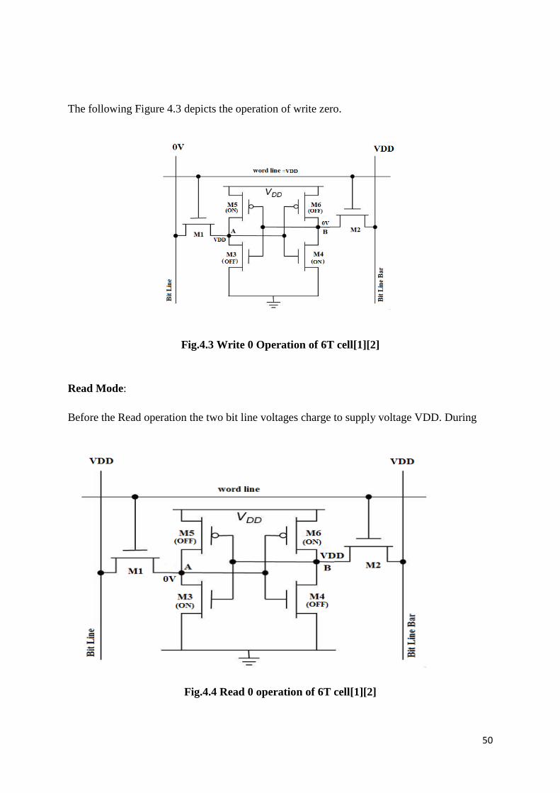
50
The following Figure 4.3 depicts the operation of write zero.
Fig.4.3 Write 0 Operation of 6T cell[1][2]
Read Mode:
Before the Read operation the two bit line voltages charge to supply voltage VDD. During
Fig.4.4 Read 0 operation of 6T cell[1][2]

51
read mode, suppose if we want to perform read 0 operations, then assume initial data stored
in the memory cell is logic 0.The figure 4.4 depicts the read zero operation of 6T SRAM Cell
and the initial voltages present at the storing nodes A and B is 0V and VDD respectively.
Hence transistors are operated in cut-off region whereas the transistors
are operated in linear region. The pass transistors are activated by
using word line which is controlled by row decoder circuit. Now there is no current flow in
transistor why because the voltages at node B and bit line bar voltages are almost equal
which is equal to VDD. On the other hand, the transistors will exhibit a nonzero
current and the bit line voltage is discharges to ground from VDD. Now both the bit line
voltages are given to the inputs of sense amplifier[17] and it will produce logic 0 as output
why because the bit line voltage is less than the bit line bar voltage. The necessary condition
to be satisfied in the read operation is given as follows,
(
)
(
)
<
By using above two conditions (A) and (B) mathematically, we can design the 6T-SRAM
cell. Otherwise the below condition needs to be satisfied which is obtained from practical
observation in order to perform correct operation i.e. either read or write operation.
(
)
(
)
(
)
-------------------------(C)
So finally the following transistor sizes will satisfy all the above conditions (A),(B)and (C)
and perform correct read and write operations i.e.
(
)
(
)
(
)
Fig 4.5 shows the schematic of 6T-SRAM Cell and symmetrical layout structure of 6T-
SRAM Cell is shown in the Fig3.6 with cell area of cell is 4.066 but standard layout has
an area of 7.7125 . So for an array of size 32×32, the area saving in symmetrical structure
compared to standard structure is around 47.21%.

52
Schematic of 6-T SRAM Cell:
Fig.4.5 Schematic of 6T- SRAM Cell
Symmetric Layout of 6-T SRAM Cell:
Fig.4.6 symmetric Layout of 6T- SRAM Cell

53
Simulation results of 6T-SRAM Cell:
Fig.4.7 Simulation results of 6T SRAM Cell
The Fig 4.7 shows the simulation results of single SRAM cell whose frequency of
operation is 8GHz.Both the bit lines takes 20ps to pre-charge supply voltage. Then write
enable signal is enabled with a delay of 25ps and word line is enabled with a delay of 30ps.
Similarly in read operation the sense amplifier is enabled whenever the voltage difference
between two bit lines is 10% of supply voltage and sense amplifier takes 50ps to give single
ended output i.e. logic 0 or 1. So finally we can say that one operation will take around 125
ps. Hence frequency of operation of SRAM Cell is 8GHz. In this project 16Kb SRAM
memory is designed using banking method which operates at 1GHz frequency.

54
The table 4.1 shown below indicates the power analysis of SRAM cell in both pre layout
and post layout simulations.
S.NO Description Pre-layout simulations Post layout simulations
1 Write 1 power 13.20 f Watt 14.12 f Watt
2 Read 1 power 4.23 f Watt 5.86 f Watt
3 write 0 power 14.13 f Watt 15.26 f Watt
4 read 0 power 4.982 f Watt 5.032 f Watt
5 Total transient power 36.55 f Watt 39.86 f Watt
6 frequency 8GHz 8GHz
Table 4.1 Comparison of Power analysis of single SRAM Cell
4.2. Stability Analysis of 6T- SRAM Cell:
The stability of SRAM cell can be decided by mostly three parameters i.e. Static Noise
Margin (SNM), Read Margin (RM) and Write Margin (WM).cell ratio (CR) and pull-up
ratio(PR) are two parameters which effects the above three parameters.
Static Noise Margin:
Static noise margin is used to measure the stability of memory cell in the presence of
Noise. It can be defined as the minimum voltage that can be applied at storing nodes so that
flipping of state occurs. By using the voltage transfer characteristics of two inverters present
in the memory cell we can calculate SNM [3]. The inverters present in the memory cell are
used to keep up stable states and their output nodes hold the information stored in the
memory cell Because of the noise exists at storing nodes the node voltages starts fluctuating

55
and stability of cell degrades. The SNM measures the permitted levels of the noise voltages
and accordingly the capacity of these inverters to hold their state in the vicinity of noise.
Fig.4.8 static noise margin representation of 6T-cell
The SNM of SRAM cell can be calculated by using Butter fly method which is shown in the
above figure4.8. It can be calculated by inserting largest possible square in between VTC of
two inverters as shown in above graph, then the side of Square is given as SNM of cell and it
is calculated as 0.24V for a supply voltage of 1V. Cell ratio, pull up ratio and power supply
are the three important parameters which affects the noise margin [3] of the memory cell.
Around seventy per cent of noise margin value is responsible by the driver
transistors, . Cell ratio is defined as the ratio of (W/L)’s of driver transistor [8]
( ) to access transistor ( ).
Cell ratio (CR) = (
)
(
)
= (
)
(
)

56
Whereas Pull-up ratio is defined as the ratio of (W/L)’s of load transistors ( ) to
access transistors ( ).
Pull-up ratio (CR) = (
)
(
)
= (
)
(
)
The SNM of cell is increasing by increasing the values of pull-up ratio and cell ratio. The
tables 4.2 & 4.3 drawn below demonstrate the dependence of above two parameters on SNM.
S. No Cell Ratio(CR) SNM(mV)
1 0.8 231
2 1 236
3 1.5 240
4 1.6 242
5 1.8 248
Table4.2 Cell Ratio vs. SNM
Table4.3 Pull-up Ratio vs. SNM
S. No Pull-up Ratio(PR) SNM(mV)
1 0.5 231
2 1 240
3 1.5 248
4 2 251
5 3 255

57
The value of SNM of cell can be increased by enhancing the threshold voltages of MOS
devices but enhancement of is limited why because it is very difficult to operate
MOSFET with higher threshold voltage.
Read Noise Margin:
This is the parameter which indicates the stability of cell in read operation. It is a strong
function of supply voltage and threshold voltage of MOS Devices. The Value of read noise
margin can be increased by increasing the value of cell ratio.[3]
i.e.
Also read margin value can be increased by increasing pull-up ratio. So design of inverters in
the SRAM cell is vital before computing Read Noise Margin in the read operation. The sizes
of the transistors are fully decides the value of pull- up ratio. The process analysis of read
noise margin is similar to process analysis of static noise margin. For a supply voltage of 1V
the read noise margin of SRAM cell is found to be 115mV.The table4.4 shown below
explains the variation of read noise margin with the cell ratio (CR).
S. No Read Noise Margin(RNM) Cell Ratio(CR)
1. 104mV 0.8
2. 109mV 1
3. 115mV 1.5
4. 121mV 2
5. 125mV 2.4
Table4.4 Read noise Margin vs. Cell Ratio
Read Noise Margin α Cell Ratio

58
Write Noise Margin:
It is a parameter which indicates the stability of SRAM cell during write operation.
Write Noise margin is the measure of the capacity to write information into the SRAM cell.
Write margin voltage is the greatest noise voltage present at bit lines for effective write
operation. The write operation failure occurs when noise voltage exceeds the write noise
margin. Write Noise margin can be calculated as the same process that we used in the
calculation of static noise margin. [3]
For successful write operation there should be only one cross point in the Butter fly
VTC curves. Write noise margin value is equal to the dimension of side of square that can be
inserted in the Butter Fly VTC curves. For a supply voltage of 1V write noise margin value is
calculated as 425mV.
By increasing the value of pull up ratio the write noise margin value is to be increased
so design of SRAM inverters is very important before the calculation of write noise margin in
write operation. The size of transistors in memory cell decides the value of pull up ratio.
It is observed that in any situation the value of Write Noise Margin is greater than Static
Noise Margin which is greater than the value of Read Noise Margin. The table4.5 shows the
variation of write noise margin with respect to the variation of pull-up ratio.
Write Noise Margin α pull-up ratio

59
Table4.5 Write Noise Margin vs. pull-up ratio
For power obliged projects like space investigation and satellites the SRAM cell which
dissipates least power ought to be utilized while for quick processing devices the SRAM cell
which has least time delay ought to be utilized. The SRAM cell which has most extreme
SNM can be utilized as a part of the device which lives up to expectations in noisy
environment. The design of memory cell can be upgraded by trade-off between different
execution parameters like power consumption, read or write delays and area of layout. So
Design of Single SRAM Cell in the memory organisation is very important to achieve good
performance.
PVT analysis of Single 6T SRAM Cell:
The design should work under any circumstance even in worst case and the design
performance can be analysed by using Process Voltage Temperature (PVT) analysis. In the
design of integrated Circuit process corner analysis is to be performed by varying the
S. No Write Noise Margin Pull-up Ratio
1 414mV 0.6
2 419mV 0.8
3 425mV 1
4 431mV 1.2
5 438mV 1.5

60
Parameters, for example Doping Concentration is varied with three or six sigma
variation. The tables 4.6, 4.7 and 4.8 had shown below shows the PVT analysis of 6T SRAM
cell.
Table 4.6 Process Corner Analysis
Power
Process
TT
FF
SS
FNSP
SNFP
Total 36.55 f W 26.524 f W 40.34 f W 35.26 f W 33.197 f W
Write 1 13.2 f W 9.04 f W 14.07 f W 12.83 f W 10.88 f W
Read 1 4.23 f W 3.12 f W 4.82 f W 3.92 f W 4.147 f W
Write 0 14.13f W 11.22 f W 15.56 f W 13.72 f W 13.96 f W
Read 0 4.98 f W 3.144 f W 5.89 f W 4.79 f W 4.21 f W
Table 4.7 Temperature Analysis
Power
Temperature
C C C C
Total 34.97 f W 35.25 f W 36.22 f W 36.54 f W
Write 1 12.87 f W 12.93 f W 13.08 f W 13.2 f W
Read 1 4.02 f W 4.13 f W 4.19 f W 4.23 f W
Write 0 13.84 f W 13.88 f W 14.03 f W 14.13 f W
Read 0 4.24 f W 4.31 f W 4.92 f W 4.98 f W

61
Table 4.8 Variation of Power with Supply Voltage
Power
Supply Voltage
1 V 1.2 V 1.6 V 1.8 V
Total 36.54 f W 48.55 f W 118.79 f W 181.47f W
Write 1 13.2 f W 15.99 f W 44.88 f W 72.24 f W
Read 1 4.23 f W 5.97 f W 30.31 f W 53.42 f W
Write 0 14.13 f W 20.52 f W 29.23 f W 38.40 f W
Read 0 4.98 f W 6.07 f W 14.37 f W 17.41 f W
The first letter in the Corner analysis is responsible for NMOS Corner, whereas the Second
letter in corner is responsible for PMOS Corner. Totally there exist three different types of
corners such as Typical, Fast and Slow, in which Fast and Slow corners have higher carrier
mobility’s than Normal corner. In this way we can perform power analysis for various
process corners, temperature and Supply voltages.

62
5. Memory Banking

63
Monolithic architecture gives better performance up to in the order of Kb whereas for
the bigger memory designs like Mb, the monolithic architecture will not give better
performance. As the number of cells increases then the bit line and word line parasitic
capacitances increases, hence unwanted delays increases, this in turn reduces the operating
frequency. So in the design of bigger memories Memory Banking method is used which
gives better performance compared to monolithic architecture.[7] The operating frequency of
memory is reduced by a factor two as the number of rows doubles whereas the frequency of
operation is reduced by a factor of four as the number of columns doubles. Hence memory
banking which is also known as array portioning technique is used in the design of bigger
size memories. In industries, the design of bigger memories whose size is around Gb, can be
done by using some scripting languages like Perl, SKILL.
Memory partitioning is the procedure of tiling memory arrays and putting the tiles in
memory such that a greatest number of data gets to are fulfilled from local memory. Memory
banking is broadly embraced to proficiently increase the memory data transmission by
utilizing various memory banks and diminishing data access conflict. Banking distributed
arrays to guarantee the locality of reference is broadly perceived as being critical in getting
great execution on circulated memory processors. Memory banking has been considered in
the distributed registering domain for quite a long time [8, 10, 12], where information
components are divided into distinctive processors to diminish communication among the
processors. In memory banking method the large array is divided in to number of sub arrays
which are identical in size. The sub arrays are commonly referred as macros, which stores the
part of the data known as sub word. In order to get complete Word all the sub arrays are
accessed simultaneously. To design High performance SRAM the number of macros is
limited to around 16 whereas for low power SRAM design the number of macros are limited
to only one.[7]

64
Conceptually every macro is looks like basic architecture shown in figure 3.2. In that
one of the Memory Row can be selected by using word line which selects all memory cells
presents in that row and desired cell can be accessed by using column multiplexer. But in this
method the word line delay increases with the square of the number of memory cells present
in that column hence speed of memory is getting worsen. This problem can be avoided by
dividing each Macro’s into smaller sub blocks by using DWL (Divide Word Line) Method
[7].
In DWL technique the Monolithic array is partitioned into m number of blocks and
each block is operated independently hence the word line length is reduced by a factor of m,
so the word line RC delay is reduced by a factor of . Hence the frequency of operation is
increased by a factor compared to monolithic architecture.
The figure 4.1 shown below depicts the DWL architecture. In that 512 columns are
divided into 4 blocks with block size of 128 columns. Now two stages of selection is required
to access particular row. First one is a global word line , which is used to select one of the
four blocks and second one is local word line which is used to select desired word line. The
local word line which are having only 128 columns, hence its RC delay reduces.
In spite of the fact that the global word line still is almost the length of the width of
the macro it has lower delay compared to full word line because the capacitive load of global
word line is smaller. It only consider the input loading of only four global word lines rather
than complete loading of 512 cells. And at a time only one block i.e. 128 cells are activated
rather than complete memory i.e. 512 cells hence the column current is reduced by a factor of
four. The concept of DWL is used recursively in the design of bigger memory leads to
hierarchical word line decoding technique.

65
Fig 5.1 DWL (Divide Word Line architecture)[7]
In this project 16-Kb SRAM Based memory is designed by using banking method, in
which four banks are used with size of each bank is 4Kb. The layout of 16-Kb memory is
drawn and post layout simulations also completed for the complete memory. The reason for
the Memory Banking architecture presented in this project is to enhance the performance of a
system by relegating memory accesses to the disjoint memory banks and giving synchronous
clash-free memory accesses. The fig 5.2 shows the banking architecture for 16-Kb memory.
The 16kb architecture consists of four memory banks each of having a size of 4Kb
and access width of 32 bits as shown in the above figure. The memory bank of 4Kb is made
by using four 1Kb blocks and eight 4to1 Multiplexers. The individual block contains 32 rows
and 32 columns with a data width of 8bits.Out of four blocks in the memory bank; one block
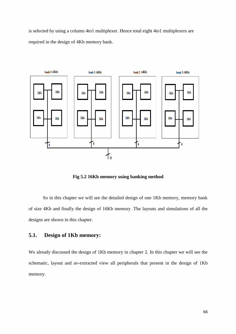
66
is selected by using a column 4to1 multiplexer. Hence total eight 4to1 multiplexers are
required in the design of 4Kb memory bank.
Fig 5.2 16Kb memory using banking method
So in this chapter we will see the detailed design of one 1Kb memory, memory bank
of size 4Kb and finally the design of 16Kb memory .The layouts and simulations of all the
designs are shown in this chapter.
5.1. Design of 1Kb memory:
We already discussed the design of 1Kb memory in chapter 2. In this chapter we will see the
schematic, layout and av-extracted view all peripherals that present in the design of 1Kb
memory.

67
5.1.1 Pre-charge:
Fig 5.3 Pre-charge schematic Fig 5.4 Pre-charge with 32 instances
Fig 5.5 Pre-charge layout

68
Fig 5.6 Pre-charge layout of 32 instances
5.1.2 Row decoder:
Fig5.7 schematic of 2to4 NOR Based Decoder

69
Fig.5.8 Layout of 2to4 NOR Based Decoder
Fig.5.9 Av-Extracted view of 2to4 NOR Based Decoder

70
Fig.5.10 Schematic of 5to32 Decoder

71
Fig.5.11 Layout of 5to32 Decoder

72
5.1.3 Word line Driver:
Fig.5.12 Schematic of Word line Driver
Fig.5.13 Layout of Word line Driver

73
Fig 5.15 Layout of word line driver (32 instances)
Fig5.14 schematic of word line driver
(32 instances)

74
5.1.4 Sense Amplifier:
Fig.5.16 Schematic of Sense Amplifier
Fig.5.17 Layout of Sense Amplifier

75
Fig.5.18 Sense Amplifier (8 instances)
Fig.5.19 Layout of Sense Amplifier (8 instances)

76
5.1.5 Write Driver:
Fig.5.20 Schematic of Write Driver
Fig.5.21 Layout of Write Driver

77
Fig.5.22 Write Driver (8 instances)
Fig.5.23 Layout of Write Driver (8 instances)
Fig.5.24 Av- Extracted view of Write Driver (8 instances)

78
5.1.6 Column Decoder/Mux:
Fig.5.26 Layout of Column Decoder/Mux
Fig.5.25 Schematic of Column Decoder/Mux

79
Fig.5.27 Column Decoder/Mux (8 instances)
Fig.5.28 Layout of Column Decoder/Mux (8 instances)
Fig.5.29 Av-Extracted View of Column Decoder/Mux (8 instances)

80
5.1.7 Schematic of 1Kb SRAM:
Fig.5.30 Schematic of 1Kb memory
Fig.5.31 Layout of 1Kb memory

81
5.1.7.1 Simulation results of 1Kb SRAM Memory:
Fig.5.32 Simulation Results of 1Kb memory
S.NO Description Pre-layout simulations Post layout simulations
1 Write 1 power 3.522 p Watt 4.012 p Watt
2 Read 1 power 3.448 p Watt 3.996 p Watt
3 Write 0 power 3.523 p Watt 4.006 p Watt
4 read 0 power 3.533 p Watt 4.017 p Watt
5 Total transient power 14.02 p Watt 16.03 p Watt
6 frequency 1.25GHz 1GHz
Table 5.1 Power Analysis of 1Kb memory

82
5.2. Design of 4Kb Memory Bank:
Fig 5.33 Schematic of 4Kb Memory Bank
Fig 5.34 Schematic of Bank Multiplexer of 4-Kb Memory

83
Fig 5.35 Layout of Bank Multiplexer of 4Kb Memory Bank
Fig 5.36 Layout of 4Kb Memory Bank
Fig 5.37 Av-Extracted View of 4Kb Memory Bank

84
Fig 5.38 Simulation Results of 4Kb Memory Bank
S.NO Description Pre-layout simulations Post layout simulations
1 Write 1 power 14.18 p Watt 16.06 p Watt
2 Read 1 power 13.95 p Watt 15.32 p Watt
3 Write 0 power 14.31 p Watt 16.59 p Watt
4 read 0 power 14.29 p Watt 15.69 p Watt
5 Total transient power 56.46 p Watt 79.69 p Watt
6 frequency 1.25GHz 1GHz
Table 5.2 Power Analysis of 4Kb Memory Bank

85
5.3. Design of 16-Kb Memory:
Fig 5.39 Schematic of 16-Kb Memory
Fig 5.40 Layout of 16Kb Memory

86
Fig 5.41 Av-Extracted View of 16-Kb Memory
Simulation Results of 16kb SRAM based Memory:
Fig 5.41simulation results of 16kb SRAM Memory
In this way 16-Kb Memory is designed using banking method with data width of 32 bits and
it takes 1ns for one complete operation hence frequency of operation is calculated as 1 GHz.

87
6. Conclusion and Future
Scope

88
6.1. Conclusion:
In this we designed 16Kb memory using memory banking method which gives better
performance compared to monolithic architecture. The SRAM is divided in to parts such as
read data path and another one is row decoder path. The layout of complete design is drawn
in an optimised manner, such that we can achieve minimum delay in above two portions. Post
Layout simulations are completed and investigated the power analysis of complete design.
Initially single 6T SRAM cell is designed which operates at a frequency of 8GHz and PVT
analysis for the 6T cell is performed because the design of SRAM cell is the heart of whole
design. Stability analysis for single 6T SRAM is performed and designed 6T cell with static
noise margin, Read Noise Margin and Write Noise Margin of 240mV,115mV and 425mV
respectively for a supply voltage of 1V. The Layout of single cell is drawn in a symmetric
manner, such that contacts of one cell are shared with contacts of another cell while making a
cell row and cell array. Hence layout area of cell array is minimised which results reduction
in the power dissipation of circuit.
All peripherals like pre-charge, row decoder, word line driver, column multiplexer,
write driver and sense amplifier are designed .The layouts of all above peripherals are drawn
in an optimised manner and individual simulations of all designs are performed. The
Frequency of memory is affected with number of rows and columns i.e. frequency of
operation is divided by a factor of two as number of rows doubles and similarly frequency is
reduced by a factor of four when number of columns doubles, hence memory banking
method is used in the design of 16Kb to achieve better frequency of operation.

89
6.2. Future Scope:
Bigger memories up to the order of Mb can be designed by with the above 16Kb
memory block by using the techniques memory banking and Butter Fly method. Whereas the
design of bigger memories beyond the range of Mb such as Gb can be designed by using
scripting languages like Perl and SKILL [25] because the layout design of such a bigger
memories could not be drawn with the hands of a man. Hence in industries the bigger
memory designs can be automated by using scripting languages to achieve better
performance. SKILL language is used to draw the layouts of the bigger memories, in which
layout of design is automatically drawn by giving some simple commands.

90
Bibliography
[1]. Sung-Mo Kang and Yusuf Leblebici ‖CMOS Digital Integrated Circuits‖, TATA
McGRAW-HILL EDITION 2003.
[2]. Jan M.Rabaey Anantha Chandrakasan Borivoje Nikolic ‖Digital Integrated Circuits‖,
Pearson Education Electronics ,2003.
[3]. Debasis Mukherjee,Hemanta Kr.Mondal,‖Static Noise Margin Analysis of SRAM Cell
For High Speed Application‖, IJCSI International Journal of Computer Science Issues,
Vol. 7,Issue 5,September 2010.
[4]. N. C. Li, et. al., ―CMOS tapered buffer‖, IEEE Journal of Solid State Circuits, vol.25,
no. 4, pp. 1005-1008, August 1990.
[5]. J. Choi, et. al., ―Design of CMOS tapered buffer for minimum power-delay product‖,
IEEE Journal of Solid State Circuits, vol. 29, no. 9, pp. 1142-1145, September 1994.
[6]. B. S. Cherkauer and E. G. Friedman, ―A unified design methodology for CMOS
tapered buffers‖, IEEE Journal of Solid State Circuits, vol. 3, no. 1, pp. 99-110, March
1995.
[7]. M. Yoshimoto, et. al., ―A 64kb CMOS RAM with divided word line structure‖, I983
IEEE International Solid State Circuits Conference, Digest of Technical Papers, pp.
58-59.
[8]. The Invention of the Intel 1103 - The World's First Available DRAM Chip By Mary
Bellis‖ [Online]. Availabe: http://inventors.about.com/library/weekly/aa100898.html
[9]. T. Wada, et al., ―An analytical access time model for on-chip cache memories,‖ IEEE
JOURNAL OF SOLID-STATE CIRCUITS, VOL. 27. NO. 8, AUGUST 1992.

91
[10]. S. Verdoolaege, H. Nikolov, and T. Stefanov, "pn: A Tool for Improved Derivation of
Process Networks," EURASIP Journal on Embedded Systems, vol. 2007, pp. 1-13,
2007.
[11]. Katsuro Sasaki, Kiyotsugu Ueda, Koichi Takasugi, et al, ‖ A 16-Mb CMOS SRAM
with a 2.3 µ Single-Bit-Line Memory Cell‖ IEEE Journal Of Solid-State Circuits,
Vol. 28, No. 11, November 1993.
[12]. Rakesh Dayaramji Chandankhede ―Design of High Speed Sense Amplifier for
SRAM‖, 2014 IEEE International Conference on Advanced Communication Control
and Computing Technologies (ICACCCT).
[13]. Kunihiko Yamaguchi, Hiroaki Nambu, et. al. ―A 1.5-ns Access Time, 78-pm’
Memory-Cell Size, 64-kb ECL-CMOS SRAM‖, IEEE Journal of Solid-State Circuits,
Vol. 27, No.2. February 1992
[14]. Sreerama Reddy G M, P Chnadrasekhara Reddy, ‖Design and implementation of 8K-
bits Low Power SRAM in 180nm Technology ‖,Proceedings of the International
MultiConference of Engineers and Computer Scientists 2009 Vol II IMECS
2009,March 18-20,2009
[15]. K. Khare, N. Khare, V. Kulhade and P. Deshpande, ―VLSI Design And Analysis Of
Low Power 6T SRAM Cell Using Cadence Tool,” leSE, lohor Bahru, Malaysia, 2008.
[16]. Taehui Na, S. Woo, J. Kim, H. Jeong, and S. Jung, ―Comparative Study of Various
Latch- Type Sense Amplifiers,‖ IEEE Trans. On VLSI Systems, vol. 22, no. 2, pp. 425-
429, Feb. 2014.

92
[17]. Ya-Chun Lai and Shi-Yu Huang, ―A Resilient and Power-Efficient Automatic Power
down Sense Amplifier for SRAM Design,‖ IEEE Trans. On Circuits & Systems, vol.
55, no. 10, pp. 1031-1035, Oct. 2008.
[18]. K.W. Mai, et al. ―Low-power SRAM design using half-swing pulse-mode techniques‖,
IEEE Journal of Solid State Circuits, vol. 33, no. 11, pp. 1659-1671, November 1998.
[19]. S. E. Schuster, et. al., ―A 15-ns CMOS 64K RAM‖, IEEE Journal of Solid State
Circuits, vol. sc-21, no. 5, p. 704-711, October 1986.
[20]. www.cypress.com
[21]. www.wikipedia.org
[22]. www.nptel.ac.in
[23]. Achiranshu Garg and Tony Tae-Hyoung Kim ‖ SRAM Array Structures for Energy
Efficiency Enhancement‖, IEEE TRANSACTIONS ON CIRCUITS AND
SYSTEMS—II: EXPRESS BRIEFS, VOL. 60, NO. 6, JUNE 2013
[24]. Byung-Do Yang ―A Low-Power SRAM Using Bit-Line Charge-Recycling for Read
and Write Operations‖, IEEE JOURNAL OF SOLID-STATE CIRCUITS, VOL. 45,
NO. 10, OCTOBER 2010
[25]. Koichi Takeda, Yasuhiko Hagihara, et.al, ―A Read-Static-Noise-Margin-Free SRAM
Cell for Low-VDD and High-Speed Applications‖, IEEE JOURNAL OF SOLID-
STATE CIRCUITS, VOL. 41, NO. 1, JANUARY 2006.
[26]. Chua-Chin Wang , Ching-Li Lee et.al ―A 4-kb Low-Power SRAM Design With
Negative Word-Line Scheme‖, IEEE TRANSACTIONS ON CIRCUITS AND
SYSTEMS-I: REGULAR PAPERS, VOL. 54, NO. 5, MAY 2007

93
[27]. Maziar Goudarzi and Tohru Ishihara, ―SRAM Leakage Reduction by Row/Column
Redundancy Under Random Within-Die Delay Variation‖, IEEE TRANSACTIONS
ON VERY LARGE SCALE INTEGRATION (VLSI) SYSTEMS, VOL. 18, NO. 12,
DECEMBER 2010
[28]. Henry Park and Chih-Kong Ken Yang ―Stability Estimation of a 6T-SRAM Cell Using
a Nonlinear Regression‖, IEEE TRANSACTIONS ON VERY LARGE SCALE
INTEGRATION (VLSI) SYSTEMS, VOL. 22, NO. 1, JANUARY 2014.
[29]. Bharadwaj S. Amrutur and Mark A. Horowitz ‖Speed and Power Scaling of SRAMs‖,
IEEE TRANSACTIONS ON SOLID-STATE CIRCUITS, VOL. 35, NO. 2,
FEBRUARY 2000
[30]. Zhiyu Liu and Volkan Kursun‖ Characterization of a Novel Nine-Transistor SRAM
Cell‖, IEEE TRANSACTIONS ON VERY LARGE SCALE INTEGRATION (VLSI)
SYSTEMS, VOL. 16, NO. 4, APRIL 2008
[31]. Masanao Yamaoka, Ryuta Tsuchiya et.al, ―SRAM Circuit With Expanded Operating
Margin and Reduced Stand-By Leakage Current Using Thin-BOX FD-SOI Transistors‖
IEEE JOURNAL OF SOLID-STATE CIRCUITS, VOL. 41, NO. 11, NOVEMBER
2006.
[32]. Hiroyuki Yamauchi ,‖A Discussion on SRAM Circuit Design Trend in Deeper
Nanometer-Scale Technologies‖, IEEE TRANSACTIONS ON VERY LARGE SCALE
INTEGRATION (VLSI) SYSTEMS, VOL. 18, NO. 5, MAY 2010
[33]. Jinn-Shyan Wang, Wayne Tseng et.al, ―Low-Power Embedded SRAM with the
Current-Mode Write Technique‖, IEEE JOURNAL OF SOLID-STATE CIRCUITS,
VOL. 35, NO. 1, JANUARY 2000
[34]. Hiroyuki Yamauchi, Toru Iwata et.al, ―A 0.5 V Single Power Supply Operated High-
Speed Boosted and Offset-Grounded DataStorage (BOGS) SRAM Cell

94
Architecture‖,IEEE TRANSACTIONS ON VERY LARGE SCALE INTEGRATION
(VLSI) SYSTEMS, VOL. 5, NO. 4, DECEMBER 1997
[35]. Hiroalu Nambu, Kazuo Kanetani et.al, ―A 0.65-ns, 72-kb ECL-CMOS RAM Macro for
a 1-Mb SRAM‖, IEEE JOURNAL OF SOLID-STATE CIRCUITS, VOL. 30, NO. 4,
APRIL 1995
[36]. Uk-Rae Cho, Tae-Hyoung Kim et.al, ―A 1.2-V 1.5-Gb/s 72-Mb DDR3 SRAM‖, IEEE
JOURNAL OF SOLID-STATE CIRCUITS, VOL. 38, NO. 11, NOVEMBER 2003
[37]. T. K. Carns, X. Zheng et.al, ―A Novel High Speed, Three Element Si-Based Static
Random Access Memory (SRAM) Cell‖, IEEE ELECTRON DEVICE LETTERS,
VOL. 16, NO. 6, JUNE 1995
[38]. Bharadwaj S. Amrutur and Mark A. Horowitz, ―A Replica Technique for Wordline and
Sense Control in Low-Power SRAM’s‖, IEEE JOURNAL OF SOLID-STATE
CIRCUITS, VOL. 33, NO. 8, AUGUST 1998
[39]. Hiroaki Nambu, Kazuo Kanetani,et.al,―A 1.8-ns Access, 550-MHz, 4.5-Mb CMOS
SRAM‖, IEEE JOURNAL OF SOLID-STATE CIRCUITS, VOL. 33, NO. 11,
NOVEMBER 1998
[40]. Venkatapathi N. Ray apati,Bozena Kaminska, ―Interconnect Propagation Delay
Modeling and Validation for the 16-MB CMOS SRAM Chip‖, IEEE
TRANSACTIONS ON COMPONENTS, PACKAGING, AND MANUFACTURING
TECHNOLOGY-PART B, VOL. 19, NO. 3, AUGUST 1996
[41]. J. J. Wang,R. B. Katz et.al, ―SRAM Based Re-programmable FPGA for Space
Applications‖, IEEE TRANSACTIONS ON NUCLEAR SCIENCE, VOL 46, NO 6,
DECEMBOR 1999
[42]. Hassan Mostafa, Student Member, IEEE, Mohab Anis, et.al,―Adaptive Body Bias for
Reducing the Impacts of NBTI and Process Variations on 6T SRAM Cells‖, IEEE

95
TRANSACTIONS ON CIRCUITS AND SYSTEMS—I: REGULAR PAPERS, VOL.
58, NO. 12, DECEMBER 2011
[43]. Kenichi Ohhata, Fumihiko Arakawa et.al, ―Power ReductionTechniques for a 1-Mb
ECL-CMOS SRAM with an Access Time of 550 ps and an Operating Frequency of 900
MHz‖, IEEE JOURNAL OF SOLID-STATE CIRCUITS, VOL. 35, NO. 4, APRIL
2000
[44]. Zheng Guo, Andrew Carlson et.al, ―Large-Scale SRAM Variability Characterization in
45 nm CMOS‖, IEEE JOURNAL OF SOLID-STATE CIRCUITS, VOL. 44, NO. 11,
NOVEMBER 2009
[45]. Byung-Do Yang, Lee-Sup Kim ―A Low-Power SRAM Using Hierarchical Bit Line and
Local Sense Amplifiers‖, IEEE JOURNAL OF SOLID-STATE CIRCUITS, VOL. 40,
NO. 6, JUNE 2005
[46]. Jinmo Kwon, Ik Joon Chang et.al, ―Heterogeneous SRAM Cell Sizing for Low-Power
H.264 Applications‖, IEEE TRANSACTIONS ON CIRCUITS AND SYSTEMS—I:
REGULAR PAPERS, VOL. 59, NO. 10, OCTOBER 2012
[47]. Vita Pi-Ho Hu, Ming-Long Fan et.al,―Threshold Voltage Design and Performance
Assessment of Hetero-Channel SRAM Cells‖, IEEE TRANSACTIONS ON
ELECTRON DEVICES, VOL. 60, NO. 1, JANUARY 2013
[48]. Koichiro Ishibashi, Koichi Takasugi et.al, ―A 6-ns 4-Mb CMOS SRAM with Offset-
Voltage-Insensitive Current Sense Amplifiers‖, IEEE JOURNAL OF SOLID-STATE
CIRCUITS, VOL. 30, NO. 4, APRIL 1995
[49]. Kunihiko Yamaguchi, Hiroaki Nambu et.al, ―A 1.5-ns access time, 78-μm2 memory-
cell size, 64-kb ECL-CMOS SRAM‖, IEEE JOURNAL OF SOLID-STATE
CIRCUITS, VOL 27. NO. 2. FEBRUARY 1992

96
[50]. Pramod Kolar, Member, IEEE, Eric Karl et.al,―A 32 nm High-k Metal Gate SRAM
With Adaptive Dynamic Stability Enhancement for Low-Voltage Operation‖, IEEE
JOURNAL OF SOLID-STATE CIRCUITS, VOL. 46, NO. 1, JANUARY 2011
[51]. Kevin Zhang, Member, IEEE, Uddalak Bhattacharya et.al,―SRAM Design on 65-nm
CMOS Technology With Dynamic Sleep Transistor for Leakage Reduction‖, IEEE
JOURNAL OF SOLID-STATE CIRCUITS, VOL. 40, NO. 4, APRIL 2005
[52]. Vijay Singh Baghel, Shyam Akashe ―Low power Memristor Based 7T SRAM Using
MTCMOS Technique‖, 2015 Fifth International Conference on Advanced Computing &
Communication Technologies
[53]. Chris Hyung-il Kim, Jae-Joon Kim, ―A Forward Body-Biased Low-Leakage SRAM
Cache:Device, Circuit and Architecture Considerations‖, IEEE TRANSACTIONS ON
VERY LARGE SCALE INTEGRATION (VLSI) SYSTEMS, VOL. 13, NO. 3,
MARCH 2005
[54]. Mohamed H. Abu-Rahma, Mohab Anis et.al, ―Reducing SRAM Power Using Fine-
Grained Wordline Pulsewidth Control‖, IEEE TRANSACTIONS ON VERY LARGE
SCALE INTEGRATION (VLSI) SYSTEMS, VOL. 18, NO. 3, MARCH 2010
[55]. Shoichiro Kawashima,Toshihiko Mori et.al, ―A Charge-Transfer Amplifier and an
Encoded-Bus Architecture for Low-Power SRAM’s‖, IEEE JOURNAL OF SOLID-
STATE CIRCUITS, VOL. 33, NO. 5, MAY 1998
[56]. Azeez J. Bhavnagarwala,Stephen Kosonocky et.al,‖ A Sub-600-mV, Fluctuation
Tolerant 65-nm CMOS SRAM Array With Dynamic Cell Biasing‖, IEEE JOURNAL
OF SOLID-STATE CIRCUITS, VOL. 43, NO. 4, APRIL 2008
[57]. Hassan Mostafa, Mohab Anis et.al, ―Statistical SRAM Read Access Yield
Improvement Using Negative Capacitance Circuits‖, IEEE TRANSACTIONS ON
97
VERY LARGE SCALE INTEGRATION (VLSI) SYSTEMS, VOL. 21, NO. 1,
JANUARY 2013
[58]. Fang-shi Lai and Chia-Fu Lee ―On-Chip Voltage Down Converter to Improve SRAM
Read/Write Margin and Static Power for Sub-Nano CMOS Technology‖, IEEE
JOURNAL OF SOLID-STATE CIRCUITS, VOL. 42, NO. 9, SEPTEMBER 2007
[59]. Henry Park and Chih-Kong Ken Yang ―Stability Estimation of a 6T-SRAM Cell Using
a Nonlinear Regression‖, IEEE TRANSACTIONS ON VERY LARGE SCALE
INTEGRATION (VLSI) SYSTEMS, VOL. 22, NO. 1, JANUARY 2014
[60]. Bharadwaj S. Amrutur and Mark A. Horowitz ‖Speed and Power Scaling of SRAMs‖,
IEEE TRANSACTIONS ON SOLID-STATE CIRCUITS, VOL. 35, NO. 2,
FEBRUARY 2000
[61]. Hiroyuki Yamauchi ,‖A Discussion on SRAM Circuit Design Trend in Deeper
Nanometer-Scale Technologies‖, IEEE TRANSACTIONS ON VERY LARGE SCALE
INTEGRATION (VLSI) SYSTEMS, VOL. 18, NO. 5, MAY 2010
[62]. Venkatapathi N. Ray apati,Bozena Kaminska, ―Interconnect Propagation Delay
Modeling and Validation for the 16-MB CMOS SRAM Chip‖, IEEE
TRANSACTIONS ON COMPONENTS, PACKAGING, AND MANUFACTURING
TECHNOLOGY-PART B, VOL. 19, NO. 3, AUGUST 1996
[63]. Zheng Guo, Andrew Carlson et.al, ―Large-Scale SRAM Variability Characterization in
45 nm CMOS‖, IEEE JOURNAL OF SOLID-STATE CIRCUITS, VOL. 44, NO. 11,
NOVEMBER 2009
[64]. H. Kato, M. Matsui et.al, ―SRAM Cell Stability Under the Influence of Parasitic
Resistances and Data Holding Voltage as a Stability Prober‖, IEEE JOURNAL OF
SOLID-STATE CIRCUITS, VOL. 32, NO. 2, FEBRUARY 1997

98
[65]. Eiji Morifuji, Takeshi Yoshida ,et.al,― Supply and Threshold-Voltage Trends for Scaled
Logic and SRAM MOSFETs‖, IEEE TRANSACTIONS ON ELECTRON DEVICES,
VOL. 53, NO. 6, JUNE 2006
[66]. J. J. Wang,R. B. Katz et.al, ―SRAM Based Re-programmable FPGA for Space
Applications‖, IEEE TRANSACTIONS ON NUCLEAR SCIENCE, VOL 46, NO 6,
DECEMBOR 1999


