Design Principles of RF and Microwave Filters and Amplifiers Prof. Amitabha Bhattacharya Department of Electronics and EC Engineering Indian Institute of Technology – Kharagpur Module No # 2 Lecture No # 10 Tutorial an Insertion Loss based Microwave Filter design Okay so we come to this final lecture on microwave filter. So here will see some tutorial problems, we have seen a long journey we have started from the image impedance concept and how based on image impedance the low frequency filters were designed. Then we have seen that if insertion loss based filter design in image impedances already you are we have introduced the concept to high light the importance but those problems generally you can solve yourself also in the tutorial sheets will give some problems. (Refer Slide Time: 01:22) But let us see some insertion loss based design and suppose if we want to have let us say maximally flat. A maximally flat low pass filter is to be designed for cutoff frequency 8 gigahertz, minimum attenuation of twenty db at eleven gigahertz. So how many elements are required elements means how many inductance capacitance etc whichever elements how many required. So what you said I require that minimum attenuation should be twenty db and at what frequency 11 gigahertz.
Transcript
Design Principles of RF and Microwave Filters and AmplifiersProf. Amitabha Bhattacharya
Department of Electronics and EC Engineering Indian Institute of Technology – Kharagpur
Module No # 2 Lecture No # 10
Tutorial an Insertion Loss based Microwave Filter design
Okay so we come to this final lecture on microwave filter. So here will see some tutorial
problems, we have seen a long journey we have started from the image impedance concept and
how based on image impedance the low frequency filters were designed. Then we have seen that
if insertion loss based filter design in image impedances already you are we have introduced the
concept to high light the importance but those problems generally you can solve yourself also in
the tutorial sheets will give some problems.
(Refer Slide Time: 01:22)
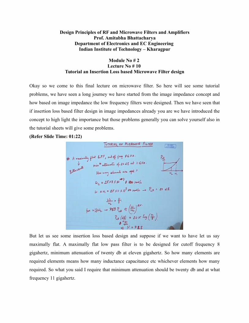
But let us see some insertion loss based design and suppose if we want to have let us say
maximally flat. A maximally flat low pass filter is to be designed for cutoff frequency 8
gigahertz, minimum attenuation of twenty db at eleven gigahertz. So how many elements are
required elements means how many inductance capacitance etc whichever elements how many
required. So what you said I require that minimum attenuation should be twenty db and at what
frequency 11 gigahertz.
What is your, cutoff frequency is given as 8 gigahertz it is a maximally flat filter a low ass filter.
So what I am saying is this is my cutoff this is my PLR, this is my omega C. But I am specifying
at certain other omega let us say 1 am specifying that it should be at least this. So you should
achieve this is omega. So let us see that what is said that, what is omega C is 2 PIE into 8 into ten
to the power ten hertz sorry 8 gigahertz.
So 10 to the power 9 gigahertz and what we want at omega = omega 1 which is equal to 2 pie
into 11 into 10 to the power of 9 hertz, not hertz omega cannot be hertz. Omega is radiant per
second, this is also radiant per second. I required that PLR should be 20 db basically this omega
1 by omega C that ratio is nothing but 11 by r. We know that for Butterworth type of polynomial
this is a maximally flat means it is actually Butterworth function we can use to synthesis.
So for omega greater than omega C we know that PLR sorry PLR can be approximated as omega
by omega C whole to the power 2n that means one term I can neglect. So, if I put it in db PLR db
that will be 20 in log omega by omega 1 by omega C. So 11 by 8, so you solve for this it is given
as 20 so 20 is equal put it as 20. So that gives you any 7.23 now N needs to be integer now
obviously it says at least 20 db so if I take N is equal to 7 it wont be at least 20 db.
So I know that since it is increasing here so since at least 20 db required i should take N should
be equal to 8. So there should be 8 order here, this is a simple one but you see this approximation
of the function at higher value that will help us to find out what is the order of the filter. Next one
let us say that again another problem that specification as maximally flat filter low pass filter,
omega C 2 gigahertz, load impedance 50 ohm and at least 15 db insertion loss at 3 gigahertz.
(Refer Slide Time: 05:50)
You see cut off frequency 2 gigahertz far away I want may be at 3 gigahertz there is some
interfering signa or into another signal source is there. So there I want to put it at least you
should have a high insertion loss of 15 db there. Now again the first thing is like before also this
is first we can find the num order N by previous method that PLR should be 1 + omega by
omega C whole to the power 2. So that is 10 to the power 15 db so solving that N we are getting
4.22.
So we will take N to be greater than equal to 5 now let us take 5 and from 5 you find the
prototype from Butterworth filter see the table for N is equal to 5 prototype values will be G =
0.618, G2 = 1.618, G3 is from the table directly you need not when that this will be given in a
problem got or as an engineer you can always refer a tables and find out what are the values G6
= 1.0.
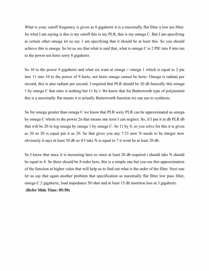
Now you scale up you know that from these values the first value. So I can draw that this will be
the circuit I have the source then the source impedance that has been said to be 50 ohm this is a
Butterworth filter. So in our prototype assumed as 1 that means G0 is always 1. But here it is 50
so you need to scale with 50 at appropriate time that means our unknown value multiplier will be
50. And then we know the first element we can choose as L1.
So let me call L1 since it will be scaled both in impedance in frequency type is same. So no type
change so I am calling it L1 dash, then this will be C2 dashed, this will be L 3 dashed, this will
be C4 dashed, then this will be L5 dashed, then I need to stop and the load impedance will be
again RL = 50 ohm. So what will be my value for L1 dashed if you see your notes this will L1
R0 omega C and what is L1? L1 is nothing but your G1 this is 0.618.
So 0.618 into 50 by omega C which is 2 pie into 2 into 10 to the power 10. So this will give you
a value of 2.46 nano henry, then C dashed will be C2 by R0 omega C now C2 you can see that it
will be 1.618 from the table 1.618 by 50 into 2 Pie into 2 into 10 to the power 9 = 2.575
picofarad. Similarly, I think now you can go on you own L3 dashed you can get the value 7.958
nano henry. C4 dashed will be 2.575 picofarad and L5 dashed is equal to 2.459 nano henry.
And so this is the example of a prototype filter design but we also scaled up prototype was first
from the table. We could have found the prototype but we have scaled up in impedance and
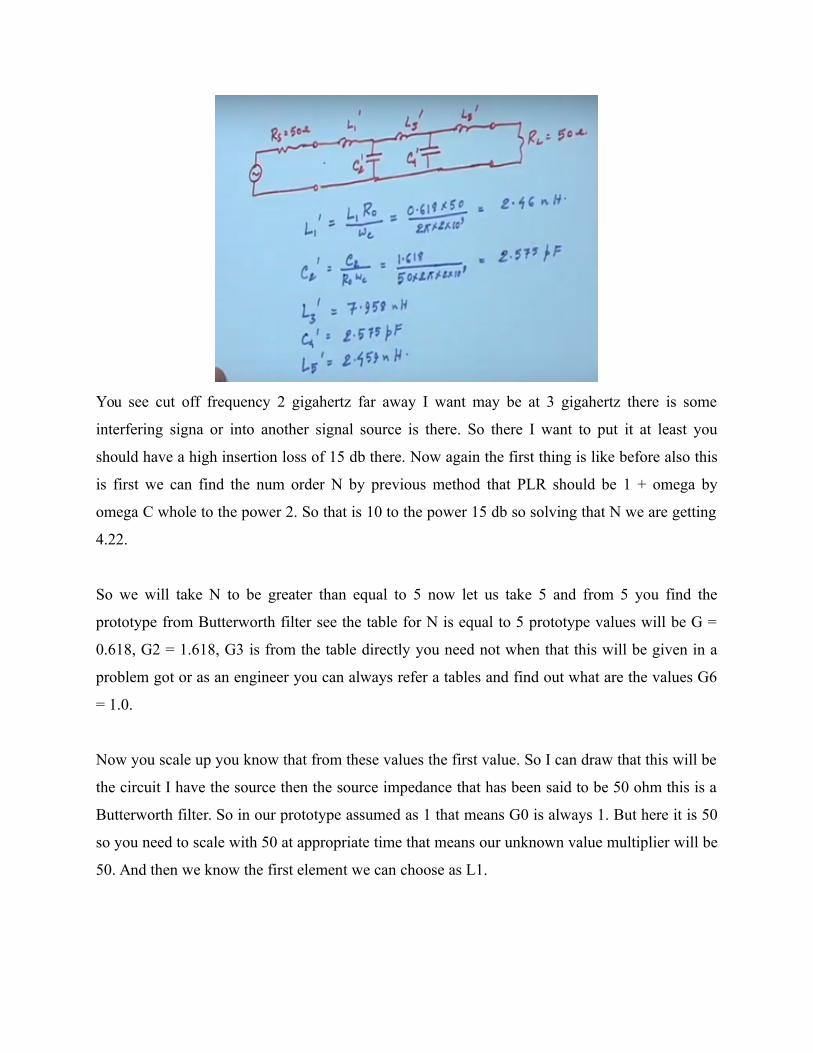
frequency. Now we will see a type change, type of thing so our third problem is this. That design
a band pass filter having a .5 db = repel response it is given that you take N = 3.
(Refer Slide Time: 11:19)
The center frequency that means our W0 is 1 gigahertz bandwidth percentage bandwidth is 10
percent and impedance level is 50 ohm. So we can you see n = 3 said so basically we will have
how many the 4 things from table G0 always this one. So what value this okay so I can take the
circuit is like this. First element if I take L1 dash second because this is band pass so I know any
L1 is basically L1 C1 dashed. Then L2 is L2 dashed C2 dashed then L3 test C3 dashed and that 3
= 3 finally it will be terminated by 50 ohm.
Now where from my get all this L1C1 values from the it is equal repel so Chebyshev so I see
Chebyshev is equal to 3 I get G1 = 1.5963 that is L1. L1 of the prototype G2 that is 1.0967 = C2,
G3 = 1.5963 again from the table L3 and G4 remember it is Chebyshev with N0. So no problem
G4 will be 1 and that is nothing but your RL. Now you can easily find out L1 dash C1 dash from
L1. What is this that delta value, delta they say 10 percent that means 0.1.
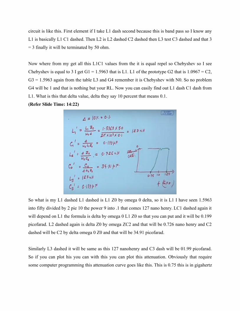
(Refer Slide Time: 14:22)
So what is my L1 dashed L1 dashed is L1 Z0 by omega 0 delta, so it is L1 I have seen 1.5963
into fifty divided by 2 pie 10 the power 9 into .1 that comes 127 nano henry. LC1 dashed again it
will depend on L1 the formula is delta by omega 0 L1 Z0 so that you can put and it will be 0.199
picofarad. L2 dashed again is delta Z0 by omega ZC2 and that will be 0.726 nano henry and C2
dashed will be C2 by delta omega 0 Z0 and that will be 34.91 picofarad.
Similarly L3 dashed it will be same as this 127 nanohenry and C3 dash will be 01.99 picofarad.
So if you can plot his you can with this you can plot this attenuation. Obviously that require
some computer programming this attenuation curve goes like this. This is 0.75 this is in gigahertz
frequency 0.75, 1.0, 1.25 roughly the curve is some ripples, when it comes to 1.25 and generally
this ripple is around 0 db approximately.
So this type of graph so this is a band pass to see now let us see a another problem that suppose
that was I think four let us say band pass filter design we have seen now implementation wise
you see that design let us say a low pass filter cut off frequency 4 gigahertz third order equal
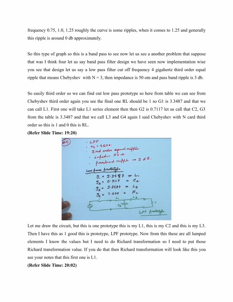
ripple that means Chebyshev with N = 3, then impedance is 50 om and pass band ripple is 3 db.
So easily third order so we can find out low pass prototype so here from table we can see from
Chebyshev third order again you see the final one RL should be 1 so G1 is 3.3487 and that we
can call L1. First one will take L1 series element then then G2 is 0.7117 let us call that C2, G3
from the table is 3.3487 and that we call L3 and G4 again I said Chebyshev with N card third
order so this is 1 and 0 this is RL.
(Refer Slide Time: 19:20)
Let me draw the circuit, but this is one prototype this is my L1, this is my C2 and this is my L3.
Then I have this as 1 good this is prototype, LPF prototype. Now from this these are all lumped
elements I know the values but I need to do Richard transformation so I need to put those
Richard transformation value. If you do that then Richard transformation will look like this you
see your notes that this first one is L1.
(Refer Slide Time: 20:02)
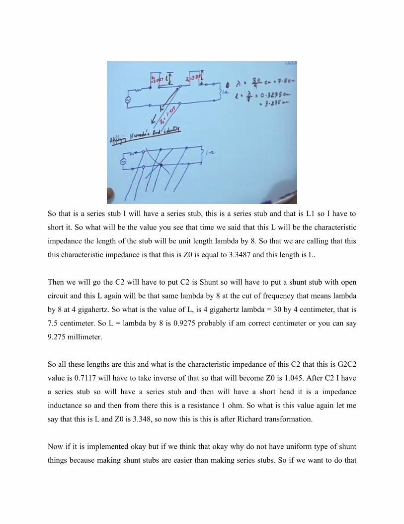
So that is a series stub I will have a series stub, this is a series stub and that is L1 so I have to
short it. So what will be the value you see that time we said that this L will be the characteristic
impedance the length of the stub will be unit length lambda by 8. So that we are calling that this
this characteristic impedance is that this is Z0 is equal to 3.3487 and this length is L.
Then we will go the C2 will have to put C2 is Shunt so will have to put a shunt stub with open
circuit and this L again will be that same lambda by 8 at the cut of frequency that means lambda
by 8 at 4 gigahertz. So what is the value of L, is 4 gigahertz lambda = 30 by 4 centimeter, that is
7.5 centimeter. So L = lambda by 8 is 0.9275 probably if am correct centimeter or you can say
9.275 millimeter.
So all these lengths are this and what is the characteristic impedance of this C2 that this is G2C2
value is 0.7117 will have to take inverse of that so that will become Z0 is 1.045. After C2 I have
a series stub so will have a series stub and then will have a short head it is a impedance
inductance so and then from there this is a resistance 1 ohm. So what is this value again let me
say that this is L and Z0 is 3.348, so now this is this is after Richard transformation.
Now if it is implemented okay but if we think that okay why do not have uniform type of shunt
things because making shunt stubs are easier than making series stubs. So if we want to do that
you see that series stub was where in Koroda’s identity yes so see kuroda’s identity so series stub
I want to make shunt stub so kuroda’s second identity I will use so using kuroda’s second
identity.
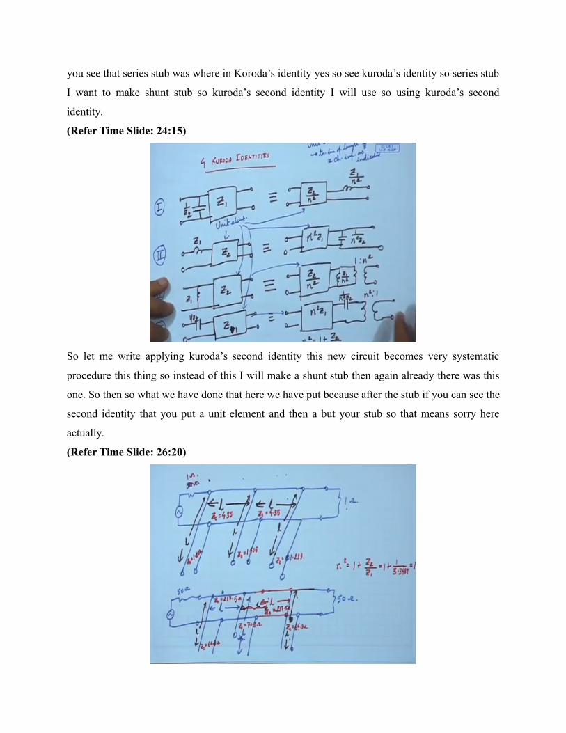
(Refer Time Slide: 24:15)
So let me write applying kuroda’s second identity this new circuit becomes very systematic
procedure this thing so instead of this I will make a shunt stub then again already there was this
one. So then so what we have done that here we have put because after the stub if you can see the
second identity that you put a unit element and then a but your stub so that means sorry here
actually.
(Refer Time Slide: 26:20)
Let me redraw because the element should be drawn first so first will have to make one unit
element and then that element will having anything then we will have our original L1. Then
again we will put another unit element and then will push that so you see this is 50 ohm these are
now I will say L length all are L lengths L is Lambda by 8. So there are three search and this is
also length L unit length this is also unit length L.
So all lengths are L only they differ by their characteristic impedance so that first one Z0 you see
that what happens to N square. N square is 1 + Z2 by Z1 and you see our Z1 our Z1 is 3.3487.so
1 + Z2 is 1 and Z3.3487 that gives the ratio as 1.299. So with this the first one will have a
characteristic impedance of 1.299 then this one if you that the Z0 for is unit element that will be
with that ratio 4.35 then this one Z0 = 1.405 and this one is Z0 =4.35 and this one is Z0 = 1.299.
This is the original capacitor, so that you see that is why this is difference but these towards
same. Now you can have the this instead of this one ohm I have impedance level as fifty ohm so
fifty this was 1 ohm, now I need to scale up to fifty ohm. So all these values I will scale up and I
will write this is fifty ohm then we will have this stub length again L and Z0 Is this 64.9 ohm just
scale up by 50 into this.
Then I will have again this is of length L a length L and this is Z0 = 70.3 ohm 1.4 into 50 ohm
then you go another, here there was one L and this L has a Z0 of 217.435. So 217 by 5 ohm then
here again this is L and again the Z0 is 7.3 L will be from here but here to here there will be
another line and there the length is L Z0 = 217.5 ohm another unit cell then we have that the
from here another stub.
So that again is Length L this length L and this stub will have Z0 = 64.9 ohm and then we will
have this fifty ohm line okay. So you see I have now see these stub and also per unit cell 2 unit
cells stub but they are not stub they are transmission lines these towards these three are three
open circuited stub this is for the first inductance, this is for the capacitance, this is for the
inductance L3 and this are unit cells. So now with length sizes are manageable I have separated
them now these unit cells are called redundant sections.
They are matched so that is why they are because they are impedances are both sides they are
matched to one that is why they do not disturb the operation of the filter. But what they do they
become separates the two so that two stub elements there is enough separation between them. So
that any in the discontinuity any high even as a modes that gives generated that can be tackle
there.
Particularly at higher level frequencies if any in discontinuity those points there is any other
modes generated that comes because this we are implementing by transmission lines but in other
microwave filters we need to do it by web guides etc there that type of problem may come. So
this completed the microwave filter design hope from the very basic point of filters just from RC
filter we have started. Then we have seen need to have LC filters for radio frequencies because
RC filters are lossy.
So went into lossless LC filters, there we have seen how to design from image impedance
concept. Then we came to the concept of characteristic impedance we said that out network will
be symmetric, will have instead of two impedance many impedances one characteristic
impedance, that characteristic impedance will try to control but we saw that there are lot of
problems of impedance matching etc, that can be tackled.
But another viewpoint is if we tackle the insertion loss if we specify the insertion loss of the
whole filter then we can synthesis any desired insertion loss characteristics and by that we have
seen first we need to do a low pass prototype filter design, and once we have low pass filter
design we can scale it up either in impedance or in frequency or in type we can change the type,
and we can have any desired type of filters with any desire it. Then we have seen that if we want
to implement it as high frequency of microwave type of filter then we need to implement not to
lumped the circuit elements but distributed circuit elements.
So how to do that we have seen thru Richard’s transformation you can do that distributed
transmission line implementation and then to have some realizable gaps or to convert one stub to
another how to do that so for that we have introduced 4 Kurodo’s identity. Any identity you need
to choose for you particular application and you apply the method is straightforward it can also
be implemented on a computer and you can do that whole things in you think that type of
simulators etc are available.
You can use that but once you know the basic principle design then you use that then it becomes
meaningful otherwise you won’t be understanding what is happening? what is the principle
microwave principles formula this is there so we hope that with this you have got a thorough
knowledge of microwave filter both it is design and implementation also you will be able to
analyze any filter design from this view point.
After this we will switch over to another very important microwave circuit thing that is amplifier
it will be an active based device design this is filter was passive but microwave amplifiers there
will active device base we will see that in the rest of this lecture series. Thank You