Det Teknisk-Naturvidenskabelige Fakultet Aalborg Universitet Basisuddannelsen TITEL: P2 project - Carbon Nanotubes PROJECT PERIOD: February 2. - May 30. 2005 PROJECT GROUP: Nano, A219 GROUP MEMBERS: Nikolaj L. Kildeby Ole Z. Andersen Tom Larsen Jacob F. Riis Ren´ e Petersen Rasmus E. Røge SUPERVISORS: Peter Fojan Lars Bo Henriksen NUMBER OF COPIES: 10 NUMBER OF PAGES: 76 NUMBER OF APPENDICES 6 TOTAL NUMBER OF PAGES 98 SYNOPSIS: This project is based on the initiating problem: “Which problems concern- ing integration of carbon nanotubes in products exists?” The theory behind characterization of CNTs and their electrical-, mechanical-, optical- and vi- brational properties is explained and a description of syntheses techniques and growths mechanisms is made. To de- scribe the electron structure of CNTs a quantum mechanical model is applied. A solution of HiPCO produced SWNTs in a D 2 O 1% SDS solution is used. The solution was sonicated and cen- trifuged to separate CNT bundles and precipitate aggregates. The techniques absorbance-, fluorescence-, Fourier transform infrared- and Raman spectroscopy is used. Atomic force microscopy and scanning electron mi- croscopy is also used. The techniques are used to determine if the CNTs are separated and to characterize CNTs. On the theoretical level a description of these techniques are in the related appendices. Considerations about the setup of the equipment are described, and the experiments are discussed. The conclusion of the report is that the SDS solution can be used to separate the CNT bundles. This is documented by the FTIR and SEM results. Fur- thermore it is shown that Raman- and absorbance spectroscopy can be used to characterize CNTs. It is also concluded that at the nanoscale it is difficult to get valid data.
Transcript
Det Teknisk-Naturvidenskabelige FakultetAalborg Universitet
Basisuddannelsen
TITEL:P2 project - Carbon Nanotubes
PROJECT PERIOD:February 2. - May 30. 2005
PROJECT GROUP:Nano, A219
GROUP MEMBERS:Nikolaj L. KildebyOle Z. AndersenTom LarsenJacob F. RiisRene PetersenRasmus E. Røge
SUPERVISORS:Peter FojanLars Bo Henriksen
NUMBER OF COPIES: 10
NUMBER OF PAGES: 76
NUMBER OF APPENDICES 6
TOTAL NUMBER OF PAGES 98
SYNOPSIS:This project is based on the initiatingproblem: “Which problems concern-ing integration of carbon nanotubes inproducts exists?” The theory behindcharacterization of CNTs and theirelectrical-, mechanical-, optical- and vi-brational properties is explained and adescription of syntheses techniques andgrowths mechanisms is made. To de-scribe the electron structure of CNTs aquantum mechanical model is applied.A solution of HiPCO produced SWNTsin a D2O 1% SDS solution is used.The solution was sonicated and cen-trifuged to separate CNT bundlesand precipitate aggregates. Thetechniques absorbance-, fluorescence-,Fourier transform infrared- and Ramanspectroscopy is used. Atomic forcemicroscopy and scanning electron mi-croscopy is also used. The techniquesare used to determine if the CNTs areseparated and to characterize CNTs.On the theoretical level a descriptionof these techniques are in the relatedappendices. Considerations about thesetup of the equipment are described,and the experiments are discussed.The conclusion of the report is that theSDS solution can be used to separatethe CNT bundles. This is documentedby the FTIR and SEM results. Fur-thermore it is shown that Raman- andabsorbance spectroscopy can be used tocharacterize CNTs. It is also concludedthat at the nanoscale it is difficult toget valid data.
Preface
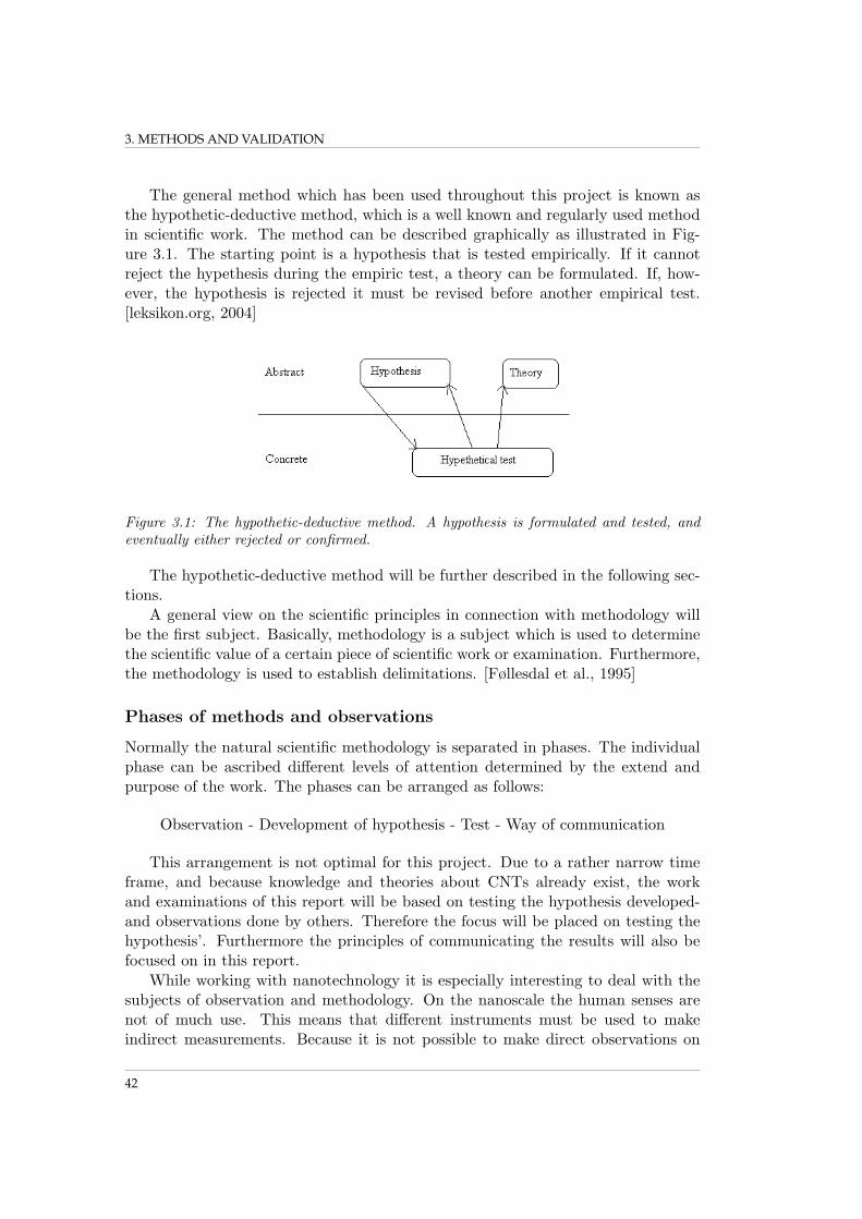
This report is the product of the P2 project period on the basis year of “AalborgUniversity - Faculty of Engineering and Science”, and it has been published by groupA219. The purpose of this project is to examine carbon nanotubes as described inthe project catalog. The carbon nanotubes used in this project are produced by theHiPCO method. The work that makes the foundation of this report has been goingon from February 2th to May 30th, 2005.
The report is for the technically interested reader with a basic knowledge of chem-istry and physics, who wants to learn about carbon nanotubes.
The report is build up of an introduction to carbon nanotubes, a problem analysisdescribing the structure and properties of carbon nanotubes, a method chapter whichdeals with the scientific method and explains the change of paradigm to quantumphysics, a chapter with the materials and methods, a results chapter, a discussionof the results, a conclusion and a perspective chapter. Finally there are differentappendices, which describe the techniques thoroughly and technically. There will bereferences from the report to appendices where appropriate. The experiment datanot present in this report can be found on the enclosed CD.
The notation used to references sources is the Harvard method.
We would like to thank Lars Rosgaard Jensen for helping with Raman spectroscopyand Maj-Brit Borksted for helping with electron microscopy.
One of the most famous quotations in nanotechnology is the phrase: “There’s Plentyof Room at the Bottom”. This quote came from Richard F. Feynman in his famousspeech to the American Physical Society in 1959. One of his points in this speechwas why no one had been able to write the British Encyclopedia on a pin head. Inregard to this Feynman arranged a competition with a price of 1000 dollars, to theperson who would first be able to write the British Encyclopedia to a pin head andthen read it again. To do this, a new kind of technology, nanotechnology, had to beused, and in 1985 a group of scientists from the Stanford University in USA couldcollect the award [www.ing.dk, 2005]. This was the first major step in the field ofnanotechnology and since then, research and studies has exploded.
One of the main areas in nanotechnology is the possibility to manipulate andmake structures on the nanoscale. This can be used to replace or improve the ma-terials used today. One of the new materials originating from nanotechnology iscarbon nanotubes (CNTs). Because of their exceptional conductive and mechanicalproperties, they have been researched and studied thorough since they were discov-ered in 1991. The properties of CNTs are dependant on several characteristics, suchas diameter, length, and chirality. CNTs can be single or multi walled (cylindersnested within other cylinders). Some of the issues regarding CNTs are how to pro-duce and characterize them in such a way, that they can be used to produce newmaterials and improve existing ones.
1.2 Initiating Problem
As pointed out in the project description there seems to be potential in the use ofCNTs in various applications. This leads up to the initiating problem:
• Which problems concerning integration of CNTs in products exists.
5
Chapter 2
Problem Analysis
2.1 Carbon Nanotubes in a Historic View
The first step in the discovery of SWNT was the identification of the C60 struc-ture of carbon by Harry Kroto and Richard Smalley. Kroto was fascinated by theprocesses occuring on the surfaces of stars and Smalley’s main work was in synthe-sizing clusters mainly of silicon and gallium arsenide, but he also had an interest invaporization of carbon. These interests brought them together at Rice Universityin 1985 in a series of experiments leading to the discovery of the C60 molecule, alsocalled the buckyball. Using laser vaporization of graphite in a helium atmospherethey produced a carbon soot which they analyzed using mass spectrometry. Theydetected a large amount of molecules containing 60 carbon-atoms but it was notuntil they realized the possibility of this structure being a closed sphere, of uniquestability and symmetry, they realized the significance of the discovery. More infor-mation about the structure and nature of the buckyball can be found in Section2.2.
Harry and Smalley’s work was published in an article in Nature in November1985 [Harris, 1999]. The next step was to discover a way of producing the C60 struc-tures in larger scale and not minuscule as was the case at Rice University. This wasaccomplished by a process far more simple than the one used in the experiment ofKroto and Smalley at Rice University. Wolfgang Kratschmer and Donald Huffmanused a simple carbon arc to vaporize graphite and it was possible to produce crys-tallized fullerenes by dispersing the soot in benzene and precipitating the fullerenesof the solution. This was published in their article in Nature in 1990 showing macro-scopic amounts of fullerenes, stimulating a boost in research. CNTs is one of thefruits of the increased research of buckyballs. [Harris, 1999]
Sumio Iijiama is credited the discovery of CNTs. Inspired by the Kratschmer andHuffman article in Nature and from previously discovered novel nano structures inthe soot produced by a similar arc evaporation process, he decided to investigate thesoot using TEM microscopy. At first he focused on the wall soot and disappointinglyfound mainly amorphous structure and not the novel structures he was looking for.
6
2.2. BUCKYBALL
This turned his attention elsewhere and he began studying the hard cylindricaldeposit formed on the graphite cathode. Here he found a variety of novel carbonstructures including the multiwalled carbon nanotube (MWNT). This was publishedin an article in Nature in November 1991.
In 1993 two groups independently discovered the single walled nanotube (SWNT).Sumio Iijiama and Toshinari Ichihashi of NEC, and Donald Bethune and colleaguesof the IBM Almaden Research Center in California was responsible for this discov-ery. The SWNT has proven to resemble the ideal nanotube both in structure andin properties. The focus of this report will be placed on SWNTs.
2.2 Buckyball
Buckyballs are a group of carbon molecules consisting of 20 to 500 carbon atomsarranged in a hollow sphere. The carbon atoms are organized in pentagons andhexagons. All buckyballs contain 12 pentagons and a number of hexagons, whichdepend on the amount of carbon atoms. As mentioned in the previous section C60
was the first discovered buckyball. The molecule was named after the Americanarchitect R. Buckminster Fuller, whose geodesic dome is constructed on the samestructural principles. A C60 molecule contain the required 12 pentagons and further-more 20 hexagons. This structure is similar to the pattern of a soccer ball. The C60
molecule contain the best properties of diamond and graphite, and it have inheritedthe high stability of diamond and the excellent conducting abilities from graphite.Figure 2.1 is an illustration of the C60 buckyball. [www.britannica.com, 2005]
Figure 2.1: The first discovered C60 buckyball. [www.britannica.com, 2005]
2.3 Characterization
CNTs are cylinder formed carbon structures with a diameter of approximately 1nmand a length of approximately 100 µm [Jr. and Owens, 2004]. This property makesthem effectively a one dimensional structure. The CNTs are formed by carbon atomsplaced in hexagonal rings like aromatic structures, composing a flat graphene sheetthat looks like honeycombs. The sheet is rolled up to form a tube. In the end of the
7
2. PROBLEM ANALYSIS
tubes a round-shaped carbon structure, such as the Buckyball, can be used to closethe tube. This is however not always the case as the tubes can be open ended. CNTscan either be single walled, or nested inside each other. If only one individual tube ispresent, it is called a single walled carbon CNT (SWNT), and if two or more tubesare nested inside each other, they are called multi walled carbon CNTs (MWNT).
Theoretical studies of CNTs indicate the importance of the surface structureto the electrical properties (see Section 2.4 for more information on the electricalproperties). Thus, a system of naming different types of surface structure is needed.This is done using two vectors: The vector Ch and the translational vector T.
The vector Ch expresses the circumference and is defined by two integers n andm, Ch = na1 + ma2. It is best visualized through a single layer of graphene as atwo dimensional honeycomb lattice. The vectors a1 and a2 are the primitive vectorsof the lattice, see Figure 2.2. The translational vector T is perpendicular to Ch
and directs the length axis. The length of the translational vector is given by thefirst encounter of a lattice point yielding the length of the unit cell of the CNT. Bythese two vectors both the circumference and the orientation of the CNT on thehoneycomb lattice are given. This entails that different types of CNTs can be givenby the set of integers (n,m).
The diameter of a CNT can be derived from the (Ch, a1, a2) triangle yieldingEquation 2.1.
dt =|Ch|π
=√
3ac−c
√n2 +m2 + nm
π(2.1)
ac−c is the length of the C-C bonds and is equal to 1.44A in CNTs. The angle θcan be limited between zero and thirty degrees due to symmetrical reasons therebylimiting the integers n and m from (n, 0) to (n, n). (n, 0) corresponds to 0◦ andis called zig-zag CNTs. Between 0◦ and 30◦ the structure is chiral. (n, n) integerscorrespond to 30◦ and the structure is called armchair. See Figure 2.3 for examples.The example shown in Figure 2.2 is a Ch = (4, 2) CNT with T = (4,−5) anddt = 4.2A.
In Figure 2.4 the different Ch vectors and their respective pair of (n,m) integersare shown. Their conducting properties are indicated by the black dots. Note thatthe honeycomb lattice is rotated compared to Figure 2.2.
The SWNT produced today is a mixture of zig-zag, armchair and chiral CNTs.Therefore, the measured properties are average values of the bulk CNTs and notfor the individual CNTs. Today it is not possible to control the production rateof each type of CNT. Nor is it possible to seperate one type from the other. Thisis something which is needed in the future, in order to fully take advantage of theelectrical properties of SWNT. [Dresselhaus et al., 2001]
8
2.4. STRUCTURE AND PROPERTIES
Figure 2.2: The Translational vector, T and the Ch vector is shown for the (n,m) = (4, 2)CNT on the honeylattice. [Dresselhaus et al., 2001]
2.4 Structure and Properties
Due to their highly interesting characteristics CNTs are today one of the most exam-ined structures on the nano scale. They combine properties such as high strength inspite of a low stiffness, and the ability to conduct electricity with low resistance. Thissection will describe the electrical, mechanical, optical and vibrational properties ofCNTs.
Electrical properties
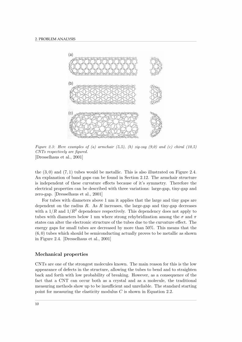
One of the most interesting aspects of CNTs are their electrical properties. TheCNTs can be either metallic or semiconducting with different size band gaps. Asdescribed in Section 2.3 these electrical properties depend on the geometric structuresuch as the diameter and chirality. The chirality is defined by the set of integers(n,m) as described in Section 2.3. In general, the armchair tubes, also called (n, n)tubes, are metallic, while (n,m) tubes with n − m = 3j, where j is a nonzerowhole number, are tiny-gap semiconductors. All others are large-gap semiconduc-tors. (1, 1) and (4, 4) tubes, for instance, are metallic, and (3, 0) and (7, 1) tubes aresmall-gap semiconductors while (5, 0) and (3, 1) tubes are large-gap semiconductors.[Dresselhaus et al., 2001]
The n − m = 3j tubes would all be metals strictly within the band-foldingscheme, but because of tube curvature effects a tiny gap opens. At room temperaturehowever, the variety in gap caused by the curvature effects would be so small thatthe n−m = 3j tubes are considered metals for practical reasons. This means that
9
2. PROBLEM ANALYSIS
Figure 2.3: Here examples of (a) armchair (5,5), (b) zig-zag (9,0) and (c) chiral (10,5)CNTs respectively are figured.[Dresselhaus et al., 2001]
the (3, 0) and (7, 1) tubes would be metallic. This is also illustrated on Figure 2.4.An explanation of band gaps can be found in Section 2.12. The armchair structureis independent of these curvature effects because of it’s symmetry. Therefore theelectrical properties can be described with three variations: large-gap, tiny-gap andzero-gap. [Dresselhaus et al., 2001]
For tubes with diameters above 1 nm it applies that the large and tiny gaps aredependent on the radius R. As R increases, the large-gap and tiny-gap decreaseswith a 1/R and 1/R2 dependence respectively. This dependency does not apply totubes with diameters below 1 nm where strong rehybridization among the σ and πstates can alter the electronic structure of the tubes due to the curvature effect. Theenergy gaps for small tubes are decreased by more than 50%. This means that the(6, 0) tubes which should be semiconducting actually proves to be metallic as shownin Figure 2.4. [Dresselhaus et al., 2001]
Mechanical properties
CNTs are one of the strongest molecules known. The main reason for this is the lowappearance of defects in the structure, allowing the tubes to bend and to straightenback and forth with low probability of breaking. However, as a consequence of thefact that a CNT can occur both as a crystal and as a molecule, the traditionalmeasuring methods show up to be insufficient and unreliable. The standard startingpoint for measuring the elasticity modulus C is shown in Equation 2.2.
10
2.4. STRUCTURE AND PROPERTIES
Figure 2.4: This illustrates some of the possible vectors in a CNT specified by the integers(n,m). It shows the armchair structure to be metallic, while the zigzag and chiral structureare around 1/3 metallic and 2/3 semiconducting, illustrated by the encircled dots and dots,respectively. [Dresselhaus et al., 2001]
C =(
1V
) (∂2E
∂ε2
)(2.2)
Where the total energy E is a function of uniform strain ε only works for CNTs,if the strain is in the axial direction. Any other deformation induces non-uniformstrain, which yields this expression misleading. Also, the volume V is not well definedfor a hollow CNT, as the cross sectional area A can be measured in several arbitraryways, making the volume V and thus the modulus ambiguous. This uncertainty isbest eliminated by considering the internal energy in the CNT per area S of thegraphite layer instead of the volume. The two dimensional structure of the graphitelayer ensures that the area is well defined; hence the modulus C can be defined as:
C =
(1L
)·(
∂2 E∂ε2
)∫dl
(2.3)
Where L is the length of the CNT, and l is the total circumferential length ofthe graphitic layers in the cross section of the CNT. This expression corresponds toYoung’s modulus Y when no lateral traction in the CNT is present, so that Y canbe expressed as:
Y = C ·∫dl
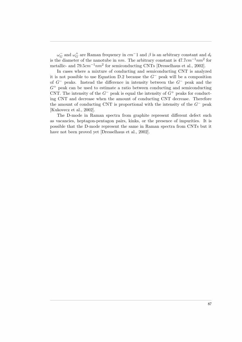
A(2.4)
Young’s modulus is a measure of the elasticity in length of a material, and isdefined as the resistance of a solid to a change in its length, which can be expressedas:
11
2. PROBLEM ANALYSIS
Y =stress
strain=
FA
∆LLi
(2.5)
Where ∆L is the change in length, Li is the original length, F is the externalforce and A is the cross-sectional area of the material [Serway and Jewett, 2004].Many different methods have been used to measure the Young’s modulus for CNTs,which is a rather challenging task. For obvious reasons, traditional methods can notbe used.
One experiment has correlated the amplitude of the thermal vibrations of thefree ends of anchored CNTs as a function of temperature with the Young’s modulus.This technique measured Young’s modulus to be around 1.8 TPa on average, butwith the significant scatter in the data, as the result varied from 0.4 to 4.15 TPafor individual tubes. Another experiment used an AFM tip to bend anchored CNTswhile measuring the force exerted by the tube as a function of its displacement. Thistest gave a Young’s modulus at 1.28 ± 0.5 TPa. An interesting observation in thistest was that the Young’s modulus showed no dependence of the diameter of thetubes [Dresselhaus et al., 2001]. Other methods have also measured Young’s modu-lus to be 1.28 to 1.8 TPa. This is a high result compared to other known substances,for example steel, which has a Young’s modulus at 0.2 TPa and aluminium at 0.07TPa [Serway and Jewett, 2004]. This indicates that CNTs indeed are strong, andit also indicates that they are hard to bend. The latter is however not quite truebecause of the low wall thickness. [Jr. and Owens, 2004].
The tensile strength of a material is a measure of the amount of stress needed topull the material apart. For SWNT the strength have been calculated to be about45 GPa, which is more than 20 times the strength of steel. [Jr. and Owens, 2004]
Vibrational properties
In a lattice all atoms undergo fluctuations from their surroundings such as heat orthermal energy. These fluctuations exist even at zero Kelvin but become more dis-tinct at higher temperatures. As chemical bonds bind atoms together, the movementfrom one atom affects another and causes this to respond to the movement. A chem-ical bond acts like a spring, meaning that it stretches and compresses. When manyatoms vibrate simultaneously their collective obtained motion spreads through-out the crystal. Each type of lattice has a characteristic frequency of vibrations[Jr. and Owens, 2004]. From the vibrations of the molecules in the CNT solution itcan be determined which molecular bonds the substance contains. This can be doneusing Fourier Transform Infrared Spectroscopy. This method is described in detailsin Appendix C.
The vibrations in CNTs have the special property that a measure of the vibra-tional frequency can be used to measure the radius of the tube. This is possiblebecause the frequencies are Raman-active and are dependant on the radius of thetube. CNTs vibrate in different ways. One of them, labeled E2g, squashes the tube.This means that it squeezes down in one direction and expands in the perpendicular
12
2.5. SYNTHESIS OF CNTS
direction essentially oscillating between a circle and an ellipse. Another mode, theA1g mode, involves an in-and-out oscillation of the tube diameter. This mode isalso known as radial breathing mode or RBM [Jr. and Owens, 2004]. Figure 2.5illustrates the RBM of the CNTs. Another vibrational mode is the tangential modeor G-band. This mode is illustrated in Figure 2.5 [Dresselhaus et al., 2002].
Figure 2.5: The figure illustrates (a) The motion of the atoms in the vibration modeof the RBM. (b) The motion of the atoms in the G-band vibration mode of the CNTs[Dresselhaus et al., 2002]
Optical properties
When light interacts with the aromatic system of the CNTs, absorption and emissionof photons takes place. At which wavelengths these phenomena appears depends onthe diameter of the CNTs. The diameter of CNTs is proportional to the wavelengthat which it absorbs and emits light. Absorption can appear without resulting emis-sion. If the (n,m) integers can be controlled to perfection, a single diameter can beproduced and this can be utilized to produce fiber optical wires with CNTs.
The interaction between light and CNTs can be monitored at different wave-lengths using absorbance- and fluorescence spectroscopy. These methods are de-scribed in Section 4.2. The data from these two methods can be used to calculate thedifferent (n,m) assignment of the CNTs present in the solution. [Bachilo et al., 2002]
2.5 Synthesis of CNTs
The potential of CNTs is indeed huge, but the full potential will not be revealed be-fore the growth of CNTs can be optimized and well controlled. Today four methodshave been developed in order to grow SWNT and MWNT, but a complete protocolfor CNT growth have not yet been developed. A hotchpotch of problems are linkedwith the production of CNTs. The primary problems are insufficient control of thestructural properties, low purity of the produced CNTs, and too high production
13
2. PROBLEM ANALYSIS
prices. To solve these problems more research in this area is needed. This sectionwill give a description of the methods.
Chemical Vapor Deposition
Chemical Vapor Deposition, or CVD for short, refers to the process of depositing agas on a surface without the gas first being condensed and liquidized. This makesdeposition the opposite process of sublimation in which a solid undergoes a phasechange from solid to gas, again, without first liquidizing. CVD has been widely usedin integrated circuit (IC) manufacturing. In IC manufacturing a thin film of silicon isdeposited on a support substrate by CVD, to create a semiconduction thin film layer.For CNT growth by CVD a somewhat different method is used, but it is still calledCVD though. Where a catalyst is almost never used for CVD manufacturing of ICdevices, CVD manufacturing of CNT always requires a catalyst [Goddard, 2003].CVD is becoming the preferred method of CNT production because of the rela-tively low temperatures needed for production. Arc-discharge for example relies ontemperatures (> 3000◦C), which is not efficient. [Dresselhaus et al., 2001]
The setup of CVD for CNT growth is pretty simple. Basically it consists of aquartz tube enclosed in a furnace. The quartz tube is typically 5− 10cm in lengthand capable of holding small substrates. The substrate being held is a supportsubstrate prepared with the catalyst. Often the support substrate is chosen to bealumina [Dresselhaus et al., 2001]. Alumina is chosen for the nanosized pores foundin its surface. The pores in alumina are filled with catalyst increasing the surfacearea and thereby the yield of CNTs. After the preparation the furnace is heated to500 − 1000◦C. Which temperature is chosen depends on the type of CNTs to beproduced. For MWNT growth a temperature of 550− 750◦C is often used, and forSWNT 850− 1000◦C is used [Dresselhaus et al., 2001]. After heating the furnace, ahydrocarbon gas is being flowed through the quartz tube. The light hydrocarbonslike methane and ethane is chosen due to their stability against self decompositionat high temperatures. This makes the decomposition of the hydrocarbon by thecatalyst the dominant process [Dresselhaus et al., 2001]. When the carbon feedstockis decomposed by the catalyst it is dissolved in the metal particles. This causesa saturation and therefore a precipitation. The precipitation of carbon from thesaturated metal particles, causes the formation of tubular graphitic sheets or CNTs.The formation of tubular sheets is preferred over plain graphitic sheets with openends. The open ends of graphitic sheets contain dangling bonds whereas the tubularsheets contain no or fewer dangling bonds and is therefore energetically favorable.An schematic setup of the CVD method described is shown in Figure 2.6.
Among the methods used for CNT growth, CVD has shown to be the mostpromising due to the high yield of nearly defect free CNTs and the possibilities ofscale-up of production. CVD is likely to be the preferred method of CNT growth inthe future.
14
2.5. SYNTHESIS OF CNTS
Figure 2.6: A schematic setup for the CVD system.
High Pressure Carbon Monoxide
SWNT can be produced by the high pressure carbon monoxide method (HiPCO).In this method carbon monoxide is used as the feedstock and iron pentacarbonyl(Fe(CO)5) as the carrier of the catalyst. The setup of HiPCO is illustrated inFigure 2.7. The two gases are lead into a furnace through a water cooled injectorat a constant flow of 1− 10 atm. The water cooled injector keeps the temperatureof the gases down until they enter the center of the furnace, where the temperatureis between 800 and 1200◦C. When the two gases enter the hot center, Fe(CO)5produce iron clusters in gas phase created by the thermal decomposition. Theseclusters act as a nucleus upon which the SWNTs starts to grow. The solid carbonis formed by the Boudouard reaction:
CO(g) + CO(g) → C(s) + CO2(g) (2.6)
It has experimentally been proved that the process can be optimized by addingan amount of preheated CO gas to the center of the furnace [Nikolaev et al., 2004].A HiPCO production yields a high amount of CNTs and the diameter of the SWNTcan vary from 0.7− 2.4nm but the width of the diameter distribution is not very re-producible resulting in an indeterminate distribution. These SWNTs are almost per-fect and without pollution in the form of fullerenes, amorphous carbon and graphite.Because of these qualities the HiPCO method is apposite for scale up of productionof SWNTs [Nikolaev et al., 2004].
Laser Ablation
Another method to produce SWNT is laser ablation. This method utilizes an in-tense laser to ablate a carbon target containing nickel or cobalt as catalyst. Figure2.8 illustrates the setup for this method. The target is placed inside a furnace,which retain a temperature of 1200◦C. During the ablation an inert gas such ashelium or argon is flown through the furnace. The gas carry the carbon atomsthough the furnace and towards a water-cooled copper collector where the atomscondense into CNTs [Dresselhaus et al., 2001]. Laser ablation can also be used toproduce MWNT. The setup is the same, except of the target, which in this case
15
2. PROBLEM ANALYSIS
Figure 2.7: A setup for the HiPCO system [Nikolaev et al., 2004]
does not contain any catalyst [Harris, 1999]. The produced CNTs have almost per-fect sidewalls but they are polluted with graphite, fullerenes and amorphous carbon.The diameter of the produced CNTs is similar to those achieved with arc-discharge[Dresselhaus et al., 2001].
Figure 2.8: A schematic picture of the laser ablation setup [www.iljinnanotech.co.kr, 2005]
Arc-Discharge
Arc-discharge was the method that Iijima used to produce fullerenes in 1991, whenhe discovered that CNTs were a by-product from this method. Since 1991 arc-discharge has been developed into a method that can produce both MWNT andSWNT [Harris, 1999]. In arc-discharge a potential of 20-25 V is applied across two
16
2.6. GROWTH MECHANISMS
1mm separated carbon electrodes of 5-20 µm in diameter, and a helium gas at 500torr pressure is flown through the system, see Figure 2.9. Carbon atoms are therebyejected from the positive electrode and form CNTs on the negative electrode. Thetemperature where this process takes place is close to the melting temperature ofgraphite, which lies between 3000 and 4000◦C [Dresselhaus et al., 2001]. MWNTcan be obtained by controlling the growth parameters under the production, suchas the pressure of the helium gas and the arcing current. Through this method itis today possible to synthesize MWNTs, which are more than ten micrometers inlength, has an inner diameter of 1 − 3nm and an outer diameter of approximately10nm. For producing SWNT with an arc-discharge system it is necessary to adda metallic catalyst. Nickel, iron, cobalt or yttrium can be used as catalyst andit is placed inside the carbon anode. The remaining setup is the same as in theproduction of MWNT. The diameter of the SWNT lies between 1.2nm and 1.4nm[Dresselhaus et al., 2001]. The arc-discharge method produces CNTs with few de-fects on the sidewalls of the CNTs. A by-product of the arc-discharge is multi layeredgraphitic particles, fullerenes and amorphous carbon. [Dresselhaus et al., 2001]
Figure 2.9: A schematic diagram of the arc-discharge apparatus[www.iljinnanotech.co.kr, 2005]
2.6 Growth Mechanisms
Today there is no method of synthesis available for large scale production of CNTs.The methods are limited by high temperatures and relatively slow reaction processes.Large scale production is however important for the integration of CNTs in industrialproducts. The current methods of synthesis have been developed on the basis of afew experimental facts, such as the need for a catalyst and enough energy to freecarbon atoms from the reagents.
The surface of the CNTs are made of hexagons and pentagons. Six pentagonsare used for closure of the CNTs while the wall of a perfect CNT consists of only
17
2. PROBLEM ANALYSIS
hexagons. If pentagons or heptagons are added in the wall of a CNT it results ina deviation from the straight structure in the form of turns or twists. A pentagonwill result in a positive curvature (convex) and a heptagon will result in negativecurvature (concave). See Figure 2.10 for examples. [Dresselhaus et al., 2001]
Figure 2.10: The result of adding a heptagon or a pentagon. [Dresselhaus et al., 2001]
Controlling the shape of a CNT through the addition of pentagons and heptagonscould be an important step in the use of SWNT, although it lies distant in the future.Through this it could become possible to control the size and shape of the SWNT.
The need for Catalysts
One of the main differences between production of SWNTs and MWNTs lies in theneed for a catalyst. This indicates a different growth mechanism between the two.Calculations have indicated that CNTs of diameter smaller than 3nm would leadto spontaneously closure if carbon is added resulting in the formation of fullerenes.Calculations have also shown that CNTs of small diameters could close sponta-neously at production temperatures between 2000K and 3000K. This indicatesthe need for catalysts in the formation of SWNTs and therefore the key to under-standing the formation of CNTs must lie in the precise role played by the catalyst.[Dresselhaus et al., 2001]
Scooter Model
In the scooter model an initiating fullerene is formed with Co or Ni atoms sittingat the open end. The diameter of the fullerene will determine the diameter of theSWNT. The diameter is set as the optimal value with respect to strain energy due tocurvature on one side and the dangling bond energy of the open edge on the other.
Calculations indicates that the Co or Ni atoms, though strongly bound, are stillvery mobile at the growing edge. This indicates that the Co or Ni atoms are scootingaround the edge of the CNT inhibiting the formation of closing pentagons.
Locally the catalytic atom is assisting the formation of hexagons and therebycatalyzing the continuous growth. However, the catalyzing effect requires singleatoms and as the concentration of metal atoms is constant several atoms will aggre-gate. This will stop the catalyzing effect and pentagons will form and close the tubeend. This aggregation will also decrease the adsorption energy of the metal clustercausing the particle to reach a critical size and “peel off”. One indicating factorin this model is that no observable metal particle is left at the tube ends. This isillustrated in Figure 2.11. [Dresselhaus et al., 2001]
18
2.6. GROWTH MECHANISMS
First principle molecular dynamics calculations of a simulation at 1500K havehowever indicated continuous closed-end growth. The metallic atom is incorporatedin the CNT cap in a frequently breaking cobalt-carbon chemical bond. In thismodel a similar principle of closing could be applied as multiple metallic atoms areincorporated and thereby loosing the catalytic effect and adsorption energy. Thisclosed-end growth is also illustrated in Figure 2.11.
Figure 2.11: To the left the scooter model is illustrated. The metallic catalyst is stronglybound though very mobile at the end of the CNT resulting in a scooting effect that preventsthe formation of pentagons. To the right the closed-end growth is illustrated. The tube asthe Cobalt-Carbon bond is breaking and reforming carbon atoms are incorporated into theCNT. Modified from [Dresselhaus et al., 2001]
Metal Covered Fullerenes as a Catalyst
Another model of the catalytic effect is the catalytic metal surface decorated fulle-rene. A fullerene adsorbing Ni or Co atoms in order to decorate the surface withthe catalytic metals could trigger the growth of a SWNT by acting as a template.The decorated fullerene would act as the template for the CNT and trigger growth.Once started the particle would not be necessary. Although the complicated appear-ance of this model the calculated average diameter, the sum of the diameter of thefullerene added two times the metal ring distance (0.7 + 2 · (0.32± 3)nm ≈ 1.4nm)is in consistency with the measured average value, 1.4nm. [Dresselhaus et al., 2001]
Vapor-Liquid-Solid
Another way of looking at the catalytic particle at the tip of the CNT is throughthe vapor-liquid-solid (VLS) model. The VLS model has its name from growingsilicon whiskers. Vapor silicon is added to a tiny catalytic droplet at the tip of
19
2. PROBLEM ANALYSIS
the filament. Silicon then precipitates from the supersatuated droplet resulting information of faceted cylinders or tubular structures. [Dresselhaus et al., 2001]
Regarding SWNT this droplet is reduced to only a few atoms, that howeverretain the catalytic effect. It is no longer fluid but the chemical reaction betweenCobalt 3d electrons and the π carbon electrons enables the rapid incorporation ofcarbon atoms.
The question of whether to find a small catalytic particle with the size of afew atoms at the tip of the CNT or not is easily answered experimentally. Thecatalytic remains has yet to be detected although the experiments cannot safely saythat there is none. However in some cases multiple CNTs are found with one sideembedded in large particles. These observations have led to the root growth model.[Dresselhaus et al., 2001]
Root Growth
During arc discharge metal and carbon particles can condense and form alloy parti-cles that when cooled will result in formation of soot particles approximately 10nmwide. These soot particles will consist of embedded metal particles surrounded bysome graphite layers. In some singularities at the surface structure the nuclei forCNTs can form growing mainly by a carbon supply from the graphite layers. Anaddition of carbon atoms at the tip is also presumed to be aiding the CNT growth.[Dresselhaus et al., 2001]
This hypothesis is supported by the fact that many SWNTs are observed to beconnected or with one side embedded in the catalytic particle. The catalytic particleis often found many times larger than the diameter of the CNT.
Neither of these models give a complete description of the catalyst role in theformation of SWNT. However the continuous interplay between experiments andtheoretical calculations continue to make improvements enhancing the insight inthese processes. The primary aim of these studies is to determine the optimalconditions for the formation of well-designed SWNT making large scale productionpossible.
A more distant goal could be to control the addition of pentagons and heptagonsto the CNT making it possible to control the shape of the CNT. [Dresselhaus et al., 2001]
2.7 CNT Bundles
Under the production of the CNTs, bundles are formed during the condensationpart of the process. The bundles are formed when the CNTs stick together due tovan der Waals forces. The reason for the strong van der Waals bonding, is that thetubes lie parallel to each other. This orientation means that the surface of contactis maximized, thereby enhancing the strength of the bundle formation. The size ofa bundle is determined by the number and size of those the CNTs interacting with
20
2.8. APPLICATIONS OF CNTS
each other. The bundle formation is what makes the raw CNTs visible to the nakedeye. [Dresselhaus et al., 2001]
2.8 Applications of CNTs
Carbon bonds are know to be strong, and the two well-known phases of solid carbon,diamond and graphite have been used widely in many applications. The transforma-tion of iron into steel by addition of carbon, to make cutting tools and for creationof high performance polymer composites for use in the aircraft industry, are justexamples of the many different uses of the traditionally known carbon structures.
The discovery of the fullerenes, and especially the CNTs, did however show thatstructures build by sp2 bonds with simple geometrical principles, results in newstructures that have fascinating and, more important, useful properties. Becauseof the high rate of flawlessness, the structure of the tubes can be fully documentedand presented from a unit cell picture. This gives the material a molecular charac-teristic, allowing scientists to predict the properties of the tubes theoretically, andencouraging experimentalists to predict and find various possible uses for the CNTs.[Dresselhaus et al., 2001]
One should be aware that the following examples of different applications ofCNTs all are predictions and visions, and therefore the extent of realization dependson different challenges that have to be coped with first. For example the price ofSWNTs still exceeds 200$ per gram [Jr. and Owens, 2004], and the amount of highpurity CNTs that can be produced is still very low. This makes the tubes tooexpensive for industrial use. Due to these reasons further investigation and researchof CNTs are essential for the development of industrial products utilizing CNTs.
In certain cases not all properties of CNTs are needed, and the productionmethod can be modified accordingly. If for example the strength is wanted fora composite material, then the purity, and to a certain extend also the separation,of the CNTs is irrelevant. If on the other hand the CNTs are wanted for their opticalproperties then both the purity and the separation are of great relevance.
Nanoprobes and Sensors
The well-defined dimensions, the electrical and thermal conductivity and the me-chanical strength and flexibility, make CNTs perfectly suitable for various formsof probes and sensors. For example applications such as high-resolution imaging,nanoelectrodes and field-emitters make use of CNT probes. Because of the size andstrength of CNTs, they can be attached to the tip of a scanning tunneling microscopeor atomic force microscope. This improves the resolution of the images, because theCNTs are thinner than the normally used silicon or metal tips. In addition to this,CNTs are very strong which minimizes the chance of breaking the tip.
However, the process of attaching a CNT at the end of an AFM tip is not an easytask. Typically bundles of CNTs are pasted on the tips and the ends are cleaved to
21
2. PROBLEM ANALYSIS
expose individual CNTs. Attempts to grow CNTs directly on silicon tips using thechemical vapor deposition method have been successful.
CNTs attached to AFM tips have shown more remarkable features. For example,pairs of CNTs positioned properly on the tip can be used like tweezers to pick up andrelease nanoscale structures. Nanolithography is another possible use; writing texton oxidized silicon substrates using CNT tips at high speeds has been accomplished.
Field emission
Field emission is when electrons are emitted at high rate from the ends of thetube. By applying an electric field parallel to the CNTs the emission is observed.This property is being used by different electronic companies for development ofhigh-technology equipment. At Samsung a flat-panel display using this feature isunder development. The flat-panel display is made by placing a thin film of CNTson top of control electronics with a phosphor-coated glass plate on top. Also, theconductivity of the CNTs can be used as shielding against electromagnetic radiation,an attribute that is currently being utilized by the US army. A plastic composite ofCNTs is under development, and is intended for the use of protection of computersand other electronic devices, as the CNTs are poor transmitters of electromagneticenergy. [Jr. and Owens, 2004]
Batteries and Fuel Cells
Using CNTs as storage for lithium and hydrogen for use in battery technology andfuel cells respectively, is another possible application. Lithium is the charge carrierin most cell phone batteries, and it is estimated that one lithium atom can be storedfor every six carbon atom in CNTs. Storing hydrogen in CNTs is a probable methodfor storage of the hydrogen atoms used in fuel cells, a potential future energy sourcefor automobiles.
A fuel cell consists of two electrodes separated by an electrolyte that disconnectshydrogen ions from its atoms, allowing only the hydrogen ions to pass through fromthe anode to the cathode. The electrons are sent through an external circuit wireto the cathode, where it combines with oxygen and hydrogen ions and form waterby which energy is released.
The fuel cells need a hydrogen source, and this source could be CNTs withhydrogen stored within it. But first a suitable method of storing hydrogen withina CNT has to be found. One promising method for this is shown in Figure 2.12.Two electrodes, of which the cathode consists of CNTs and the anode consists ofNi(OH)2, are placed in a 6MKOH water solution. The water in the electrolytesolution is decomposed into positive hydrogen ions which are bonded to the negativeCNTs. [Jr. and Owens, 2004]
22
2.8. APPLICATIONS OF CNTS
Figure 2.12: A model for an electrochemical cell used to inject hydrogen in CNTs. Thecell consist of an electrolytic solution of KOH with a negative and positive electrode. Thenegative electrode consist of CNT paper. Voltage between the electrodes causes the H+ ionto be attracted to the negative electrode.
Mechanical Reinforcements
Incorporating CNTs in aluminium is one example of improving the tensile strengthof materials. At an experiment in Tokyo aluminium powder at 5% vol. CNTs, isheated to over 800K and mixed in vacuum. Thereafter the mixture is compressedwith steel dies and extruded into rods. These rods appeared to be twice as strongas normal aluminium rods, and theoretical estimations suggests that the strengthcould be optimized by a factor 6 with proper operations. [Jr. and Owens, 2004]
The challenges to be solved before CNTs can be used in structural reinforcementsare the ability to create a good interface between the CNTs and the polymer matrix,and ensuring a good load transfer from the matrix to the CNT. The major problem isto prevent the sliding between individual layers in CNT, and the sliding of individualCNT in ropes. This indicates that CNT ropes will have to be dispersed or cross-linked internally, so that the sliding does not occur.
Sliding between the CNTs in ropes can be avoided if the length of the CNTsis big enough. In 2003 scientists at the University of Texas at Dallas proved thatstrong pure CNT fibres can be made. The scientists produced fibres made from puresingle walled CNTs. These fibres proved to be up to 4 times stronger than spidersilk, which is one of the strongest known materials. The individual CNTs within thefibres are held together by the intermolecular forces present within CNT bundles.The longer the CNTs are, the greater are the contact area between parallel CNTsand the greater are the intermolecular forces between two CNTs. It is estimatedthat to achieve fibre strengths near the intrinsic strength of CNTs, the CNT contactlength must be in the order of 10 to 120 µm. Today though, the typical length ofCNTs are only 300 nm, meaning that the strength of fibres are only a fraction ofwhat is possible [Goddard, 2003].
23
2. PROBLEM ANALYSIS
Nano memory
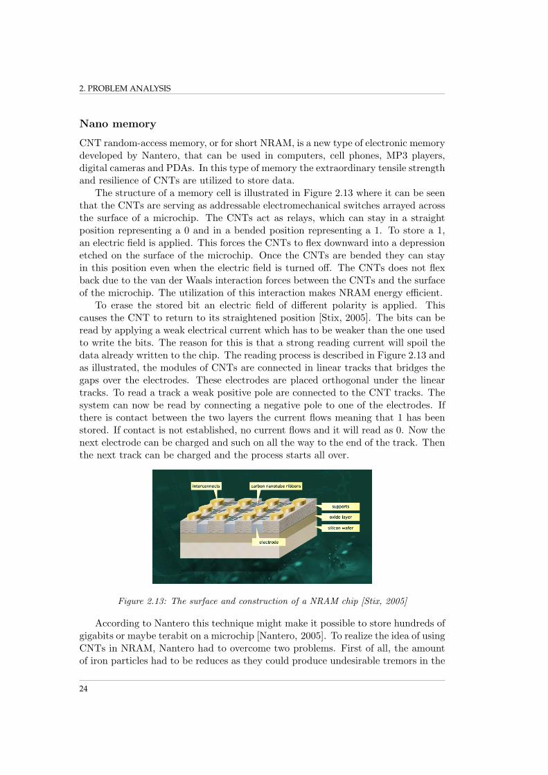
CNT random-access memory, or for short NRAM, is a new type of electronic memorydeveloped by Nantero, that can be used in computers, cell phones, MP3 players,digital cameras and PDAs. In this type of memory the extraordinary tensile strengthand resilience of CNTs are utilized to store data.
The structure of a memory cell is illustrated in Figure 2.13 where it can be seenthat the CNTs are serving as addressable electromechanical switches arrayed acrossthe surface of a microchip. The CNTs act as relays, which can stay in a straightposition representing a 0 and in a bended position representing a 1. To store a 1,an electric field is applied. This forces the CNTs to flex downward into a depressionetched on the surface of the microchip. Once the CNTs are bended they can stayin this position even when the electric field is turned off. The CNTs does not flexback due to the van der Waals interaction forces between the CNTs and the surfaceof the microchip. The utilization of this interaction makes NRAM energy efficient.
To erase the stored bit an electric field of different polarity is applied. Thiscauses the CNT to return to its straightened position [Stix, 2005]. The bits can beread by applying a weak electrical current which has to be weaker than the one usedto write the bits. The reason for this is that a strong reading current will spoil thedata already written to the chip. The reading process is described in Figure 2.13 andas illustrated, the modules of CNTs are connected in linear tracks that bridges thegaps over the electrodes. These electrodes are placed orthogonal under the lineartracks. To read a track a weak positive pole are connected to the CNT tracks. Thesystem can now be read by connecting a negative pole to one of the electrodes. Ifthere is contact between the two layers the current flows meaning that 1 has beenstored. If contact is not established, no current flows and it will read as 0. Now thenext electrode can be charged and such on all the way to the end of the track. Thenthe next track can be charged and the process starts all over.
Figure 2.13: The surface and construction of a NRAM chip [Stix, 2005]
According to Nantero this technique might make it possible to store hundreds ofgigabits or maybe terabit on a microchip [Nantero, 2005]. To realize the idea of usingCNTs in NRAM, Nantero had to overcome two problems. First of all, the amountof iron particles had to be reduces as they could produce undesirable tremors in the
24
2.9. ORBITAL SHAPES
further production. Nantero developed a complex filtration process, which reducesthe amount of iron to the parts-per-billion level. The second problem was how toplace the CNT in the right places on the microchip. Deposition of CNTs onto thewafer using gas vapor was not possible because this process requires temperatures atabout 1000 degree. This high temperature would ruin the already placed circuitry.The Nantero ended up using a coating technique where a CNT-containing solvent isspin coated onto the wafer. This technique leaves a thin film of CNTs on the waferafter the solvent is removed. Afterwards are lithography and etching used to formthe right pattern of CNTs. According to Scientific American the first commercialproduction of NRAM will take place next year [Stix, 2005].
CNTs in Light Bulbs
In June 2004, Chinese scientists managed to produce a light bulb based on highlypurified CNT filaments, instead of the traditional tungsten filaments used today.The original tungsten filament was replaced by a CNT filament in an ordinary 40-watt light bulb. The scientists found that the CNT filament emitted even morelight than traditional 40-watt light bulbs. Furthermore, the CNT filament had alower threshold for light emission than tungsten filaments. Another quite excitingdiscovery made by the scientists was that the CNT filament did not change itsresistance at temperatures up to 1750K. This discovery suggests that CNTs couldsomeday be used as high precision resistors. [Dume, 2005]
2.9 Orbital shapes
Orbitals are models, which describe the probability distribution of the electronaround the nucleus in an atom. According to Pauli’s exclusion principle each orbitalcan only contain two electrons of opposite spin. The number of orbitals attachedto each electron level in an atom is equal to the second power of the level number.The orbitals in each level are divided into subshells, which are marked s, p, d, fand g. In the first level there is only room for two electrons, which means only sorbitals occur in the first level. The p orbitals are added in level two, d orbitals inlevel three, f orbitals in level four and finely g orbitals in level five. The number oforbitals attached to each subshell is starting with one orbital in subshell s and risesby two from subshell to subshell. The shape of the s- and p-orbitals are illustratedin Figure 2.14.
As seen in Figure 2.14 the s and p orbitals are marked with 2s, 2px, 2py and2pz. 2 refers to which level the orbital belong and the letters x, y and z tells theorientation in proportion to the system of coordinates. The two first types of orbitalsare relatively simple to draw but the shape become more complex for the other typesof orbitals.
CNTs are build from carbon atoms and it is therefore important to know theelectron structure of these to get a better understanding of the CNTs and theirbindings. Carbon has the atomic number 6 and therefore has 6 electrons, which
25
2. PROBLEM ANALYSIS
Figure 2.14: The orbitals belonging to the second principal quantum number[mhhe.com, 2005].
means the electrons are placed in s and p orbitals. The first two electrons fill up the1s orbital. The last four electrons, which also are the valence electrons, are placedin the following way. Two electrons in the 2s orbital and two electron in 2p orbitals.The carbon atoms in CNTs are bonded together by covalent bonds, which normallyare described as a system where the atoms are sharing the valence electrons. Thecovalent bonds can also be described more detailed with atomic orbitals used toshare the valence electrons. The crystal lattice of CNTs can be seen as a rolledup graphene sheet and therefore it will be assumed that the bonds between thecarbon atoms are similar to the bonds in graphite. In graphite all the carbon atomsare organized in plane lattices consisting of hexagons where all the C − C bondsare known to be equivalent. To explain this fact, the three double bonds mustcontinuously shift between the carbon atoms in the hexagon. As mentioned beforethe valence electrons are placed in 2s and 2p orbitals, which mean there can be fouroverlaps of orbitals. These overlaps can be between to identical orbitals or betweena 2s and a 2p orbital.
However these overlaps will give a formation that does not corresponds to thereal formation where each carbon atoms are bonded in the plane to three othercarbon atoms with an angle of 120 degrees. To overcome this problem it makessense to assume that the carbon atoms use orbitals, that are combinations of 2s and2p orbitals. In fact a combination of a 2s orbital and two 2p orbitals makes threeorbitals in the plane with an angle of 120 degree between each other as it can beseen in Figure 2.15.
This mixing of the original orbitals to form special orbitals for bonding is calledhybridization. The three new orbitals are called sp2 because they are hybridizationof one 2s and two 2p orbitals (s1p2). After this hybridization of orbitals it is possibleto explain the bonds in the carbon hexagons where there exist two types of bonds.The first type of bonds is the sigma σ bond, which is a bond between two sp2 orbitals.In this bond the orbitals are overlapping each other and it occurs between all thecarbon atoms. The second bond is a π bond, which in this is called a delocalizedπ bond because of the electron resonance. The π bond is formed between two 2porbitals as it require less energy compared to a bond between two 2s orbitals. In thisπ bond the shared electron pair occupies in the space above and below the plane ofthe σ bonds [Zumdahl and Zumdahl, 2003]. In the case of the CNTs the curvatureand the folding angle of the graphene layer determines if the specific (n,m) folding
26
2.10. CRYSTALLINE STRUCTURE
Figure 2.15: The hybridization between 2s, 2px and 2py orbitals. The figure is modified from[mhhe.com, 2005]
of the tube gives conducting or semiconducting properties. The reason for this isthat the p orbitals interacts with each other.
2.10 Crystalline structure
A crystal is matter in the solid state where the atoms are ordered in a periodicarrangement. Ideally, it is an infinite repetition of identical atoms or of a structureof atoms. In Figure 2.16 the definition of a crystal is described. The crystal can bedescribed as if the bases where attached to points in a lattice. [Kittel, 2005]
Figure 2.16: The basis is added to the lattice forming the crystal. Note that the lattice is anet in three dimensions, while only two dimensions are displayed here. Basis + Lattice =Crystal. Modified from [Kittel, 2005]
It does not matter if the lattice is displaced as long as it fulfils the criteria ofthe lattice definition. The points of the lattice are defined by the addition of thetranslation vector to one point of the lattice:
R1 = R+ T,T = n1a1 + n2a2 + n3a3 (2.7)
a1, a2 and a3 being the unit vectors of the lattice and n1, n2 and n3 beingarbitrary integers. The translation vector, T, describes the difference between thetwo points, R and R1. The relation between two points, when suitable numbers,n1, n2 and n3 are chosen, can be described by the translation vector. This meansthat the lattice units are the smallest possible. Several lattices may be chosen for
27
2. PROBLEM ANALYSIS
one crystal. For either choice the same results of analysis including x-ray diffractionpattern ensue as long as the translation vector of Equation 2.7 has been satisfied.The crystal can be defined with basis in the growth of bases on top of each other orfrom a given lattice as long as Equation 2.7 is maintained.
In a lattice it is possible to chose several different unit cells, however, a distinctionbetween the primitive unit cell and the unit cell is necessary. The primitive unitcell is defined as minimum volume cells. Each primitive cell has only one latticepoint attached and for a given crystal the number of atoms in the primitive cell isinvariable. A normal choice of primitive cell is the parallelepiped. In Figure 2.17different primitives cells, cell 1, 2 and 3 and one nonprimitive cell 4, are shown.[Kittel, 2005]
Figure 2.17: The choice of different unit cells is possible. 1,2 and 3 are primitive cells while4 is not.[Kittel, 2005]
Figure 2.18: The cell determined by the vectors a1,a2,a3 is a primitive parallelepiped unitcell [Kittel, 2005].
For a parallelepiped primitive cell, see Figure 2.18, the number of lattice pointstouched by the primitive cell is 8, and when neighboring 8 identical cells the numberof associated lattice points must be: 8 · 1/8 = 1.
Wigner-Seitz Cell
One way of choosing the primitive cell is the Wigner-Seitz cell. Lines are drawnto connect a chosen lattice point to all nearby points. At the midpoint new linesor planes are drawn normal to the first lines. The smallest volume enclosed by the
28
2.11. CONDUCTING PROPERTIES OF SOLIDS
lines or planes drawn is defined as the Wigner-Seitz cell and it is a primitive unitcell. See Figure 2.19 for an illustration of this method. [Kittel, 2005]
Figure 2.19: The primitive unit cell constructed by the Wigner-Seitz cell.
Reciprocal space
The reciprocal space is encountered when using quantum mechanics or Fourier analy-sis. It is called either reciprocal space, the wave space or k-space from either theunit of the axes or the origin. Due to the periodicity of crystals functions of anequal periodicity is required to describe the electronic structure. This yields thatthe points in the reciprocal space are determined by 2πp/a, p ∈ Z. See Section 2.13for more about the wavefunction of electrons. The unit cells of the reciprocal spaceare given by:
b1 = 2πa2 × a3
a1 · a2 × a3;b2 = 2π
a3 × a1
a3 · a2 × a1;b3 = 2π
a1 × a2
a1 · a2 × a3(2.8)
A Wigner-Seitz cell in the reciprocal lattice is defined as a Brillouin zone. Hence,the first Brillouin zone is the primitive cell in the reciprocal lattice. [Kittel, 2005]
2.11 Conducting Properties of Solids
In solid state physics the electrical conductivity of crystals is divided into threeclasses: conductors, semiconductors and insulators. In this section the differencebetween these three classes will be discussed in terms of models based on energybands.
Fermi Levels
The value of the Fermi level at 0K is called the Fermi energy and is a constantfor each solid. According to the Pauli exclusion principle each energy level canaccommodate only two electrons. Hence, at 0K the electrons pack into the lowestpossible available energy states and build up a Fermi sea of electron energy states.The surface of the sea is the Fermi level where no electrons at absolute zero willhave enough energy to rise above the surface. The Fermi level is any energy levelhaving the property that it is exactly half filled with electrons. Levels of lower energythan the Fermi level tend to be entirely filled with electrons, whereas energy levels
29
2. PROBLEM ANALYSIS
higher than the Fermi level tend to be empty. The Fermi energy EF for an electronrestricted to motion in one dimension is defined in Equation 2.9
EF =h2
2m
(Nπ
2L
)2
(2.9)
Where N is the total number of electrons and L is the length of the line to whichthe electron is confined. For more information about this model see Section 2.12.
As the temperature rises or as electrons are added to or withdrawn from the solidthe Fermi level changes and a certain fraction of electrons will exist above the Fermilevel. This is characterized by the Fermi-Dirac distribution function. [Kittel, 2005]
Fermi-Dirac distribution function
The Fermi-Dirac distribution function f(E) gives the probability that a given avail-able electron energy state E is occupied by one of the electrons in a solid. It is givenby Equation 2.10.
f(E) =1
e(E−EF )/kbT + 1(2.10)
where kb is Boltzmann’s constant and T is the temperature measured in Kelvin.The left figure in Figure 2.20 is a plot of f(E) versus E for T = 0K and it
shows that f(E) = 1 for E < EF and that f(E) = 0 for E > EF . This illustrates,as explained in Section 2.11 that at 0K all states with energy less than the Fermienergy are occupied and all states with more energy are unoccupied.
The figure to the right of Figure 2.20 is a plot of f(E) versus E for T > 0 andit shows that as T increases, the distribution slightly rounds off. Due to thermalexcitation states near and below EF lose electrons and states near and above EF
gain electrons. [Kittel, 2005]
Figure 2.20: Plot of the Fermi-Dirac distribution function for f(E) versus E. To the left isa figure of T = 0K and to the right T > 0.
Metals
Metals are good conductors because the charge carriers, the electrons, are free tomove in response to an applied electric field. When an electric field is applied to a
30
2.11. CONDUCTING PROPERTIES OF SOLIDS
metal, the energy of the system will be increased, which corresponds to the additionalenergy of the moving electrons. Therefore, when an electric field is applied to ametal, electrons must move upward to a higher available energy state in an energy-level diagram. The bottom most energy band in Figure 2.21(a) illustrates a alf- filledenergy band in a conductor at 0 K, where the blue region represents levels filled withelectrons. The electrons in the band obey the Fermi-Dirac statistic, which meansall energy levels below the Fermi energy (EF ) are filled and no one above is filled.The Fermi energy lies in the band at the highest filled state. This distributiononly occurs a 0 K, and electrons can thermally be excited to levels above EF if thetemperature is increased slightly. This means the electrons, having energy near theFermi energy, only needs a small amount of additional energy to reach an emptyenergy state above the Fermi energy. Therefore, electrons in a metal can be free tomove when a small electric field is applied [Serway and Jewett, 2004].
(a) (b) (c)
Figure 2.21: The band structure of (a) a metal (b) an insulator and (c) a semiconductor.
Insulators
The difference between a metal and an insulator is that the energy band in aninsulator is not continuous like in a metal. The energy band of an insulator is shownin Figure 2.21(b). The highest filled energy band is called the valence band, and thelowest empty energy band is called the conduction band. The energy separating thevalence band and the conduction band is normally referred to as the energy gap orband gap. The energy gap occurs because there are no allowed energy levels in thisarea. The Fermi energy lies somewhere in the energy gap as shown in the figure.It was earlier mentioned that the Fermi energy lies in the band at the highest filledstate, and this might suggest the same placement in an insulator. The reason whythe Fermi energy is placed between the bands in an insulator can be explained by amore sophisticated treatment of the Fermi energy. The presence of the energy gapis also the reason why an insulator cannot lead a current. The energy required toexcite an electron from the valence band to the conducting band is too big to beobtained by applying an electric field. Therefore free moving electrons cannot beobtained in an insulator.[Serway and Jewett, 2004]
31
2. PROBLEM ANALYSIS
Semiconductors
The band structure of a semiconductor is illustrated in Figure 2.21(c). Like aninsulator a semiconductor have an energy gap between the valence band and theconducting band. The difference between an insulator and a semiconductor is thesize of the energy gab. The Fermi energy is placed between the two bands like in aninsulator. At 0K all the electrons in a semiconductor are placed in the valence band.When the temperature increases, an appreciable numbers of electrons are excitedinto the conduction band because the energy gap is not as large as in an insulator.There are many empty levels above the thermally filled levels, which means thata small electric field can raise the electrons in the conducting band, resulting in amoderate current. [Serway and Jewett, 2004]
2.12 Energy of the nearly free electron
The origin of band gabs can be explained using the model of the nearly free elec-tron. In order to describe this model the first thing is to look at the model of thefree electron. Consider an electron existing in a space without any influence fromother particles. Looking at this electron from a quantum mechanical point of viewthe time-independent Schrodinger equation in one dimension is of much interest.This equation is used to determine the wavefunction which describes the energy forquantum mechanical systems. See Equation 2.11.
− h2
2md2ψ
dx2+ Uψ = Eψ (2.11)
In this equation h is Planck’s constant divided by 2π, m is the mass, E is theenergy of the electron and ψ is the wavefunction. In the case of the free electron thepotential U is equal to zero. The solution of this equation is, in the case of the freeelectron, on the form seen in Equation 2.12.
ψk(x) = eikx (2.12)
Equation 2.12 describes a wave, hence the description as a wavefunction. Inrelation to quantum mechanics the solutions of these wavefunctions will often bedivided in two groups of functions; allowed and forbidden functions. The forbiddenfunctions are those at which the wavefuntion is different from 0 at the barriers. Thedivision into allowed and forbidden functions will be further described later on inthis section. In the case of the free electron there are no forbidden values of thewavefunction. The plot of the energy as a function of the wavevector k will form aparabola stretching from zero to infinity. [Kittel, 2005]
Looking at the model of the nearly free electron, compared with that of the freeelectron, there are one major difference. The nearly free electron is restrained byboundaries from the nucleus it orbits. As a result of this, only some of the wavefunc-tions will be allowed. In order for a wavefunction to be allowed it is necessary that
32
2.13. ELECTRON IN A CRYSTAL
the space defined by the model allows for either half or whole wavelengths to existin the space. In Figure 2.22 a model of the probability distribution of the nearlyfree electron potential well is illustrated and it includes the square of the three firstlegal wavefunctions.
Figure 2.22: A model of the probability distribution of the nearly free electron where the legalwavefunctions are plotted. The x-axis describes the position of the electron in relation to thenucleus and the y-axis plots the probability of finding the electron in the given position. Thehorizontal lines plotted in connection with the wavefunctions is the energy belonging to thespecific wavefunction. The boundaries at the end of each wavefunction is infinitely.
From the model it is seen that the individual wavefunction belongs to a spe-cific energy. The energy levels between the plotted functions, not occupied by awavefunction, is the earlier mentioned forbidden values. These unoccupied energiesexplain the phenomena of band gabs. If the electron of the system exists at the firstlegal energy level n = 1, the minimum energy needed to excite the electron to thenext legal energy level n = 2 is the difference in energy between the two levels ∆E,hence the size of the band gab.[Kittel, 2005]
2.13 Electron in a crystal
In order to achieve a realistic image of the band gab in a CNT it can be advantageousto investigate the model of an electron in a crystal. A CNT is constructed of aseries of primitive cells defined by the two vectors Ch and T. This is basically aone dimensional crystal with a complicated basis. The method of calculating theconducting properties is comparable with the method used in a simple 1-dimensionalcrystal.
The potential energy in this one dimensional model varies with the distance tothe nucleus in accordance with the coulomb force. An approximated model withquadrangular potential wells can be used in order to simplify the calculations re-
33
2. PROBLEM ANALYSIS
sembling multiple potential wells of finite size on a line. This model is shown inFigure 2.23 along with the borders of the Wigner-Seitz cell.
Figure 2.23: The potential energy U is shown on the y axis of the crystal. The black spheresare the atom nuclei, the E level displays the energy of the electron which is set below thepotential energy between the atom nuclei. The first Weigner-Seitz cell is between x = −a
2and x = a
2 .
According to the assumption of infinite length, translational symmetry exists andthe potential energy and the probability density must be periodic with the period a.Because the probability density of electrons is measurable this is the solution whichis found. A periodic probability density can be achieved by multiplying a periodicfunction by a complex number of modulus 1:
Furthermore, there is no change in the probability density from x to −x so thewavefunction Ψ(−x) must be equal to either −Ψ(x) or Ψ(x). The final solutionmust be a linear combination of these functions. They are named f(x) and g(x)respectively. From considerations in continuity at x = a
2 compared to x = −a2 the
following equations can be derived:
cos(ka) =fg′ + f ′g
fg′ − f ′g|x=a
2(2.15)
The solution to this is real when | cos(ka)| ≤ 1. Values out of this range is calledthe band gap. For the chosen well model it is possible to derive expressions for fand g through the Schrodinger equation and after insertion in Equation 2.15 thefollowing expression for cos(ka) can be derived:
α =√
2mEh
, β =
√2m(U − E)
h, β′ =
√2m(E − U)
h(2.16)
cos(ka) = cos(αb) cosh(β(a− b)) +β2 − α2
2αβsin(αb) sinh(β(a− b)), E < U (2.17)
cos(ka) = cos(αb) cosh(β′(a− b)) +β′2 − α2
2αβ′sin(αb) sinh(β′(a− b)), E > U (2.18)
34
2.13. ELECTRON IN A CRYSTAL
These two expressions are plotted in Figure 2.24 showing the allowed and forbid-den energies of the electron. The grey regions represents forbidden energies (bandgaps) and the white regions represent allowed energies. Each energy corresponds toa value of k, and thereby some values of k becomes allowed and some forbidden.
Figure 2.24: Equation 2.18 is plotted as a function of the energy of the electron. Onlyenergies that correspond to a cos(ka) value between −1 and 1 are allowed. Note that eachband and bandgab corresponds to a band of allowed and forbidden k values, respectively.
With Equation 2.18 it is possible to derive an approximated expression for theenergy band of electron. This is only precise for narrow bands and is displayedin Figure 2.25. Next to this figure two energy bands for CNTs are displayed as acomparison.
In each energy band there can be two electrons of opposite spin according thePauli’s exclusion principle. The six electrons of carbon must therefore be divided in3 full bands. This makes the tetrahedral structure of diamond an insulator. The Πorbital of graphite is responsible for the conducting properties which are also presentin CNTs.
35
2. PROBLEM ANALYSIS
Figure 2.25: The left image displays the energyband of the simple 1D crystal. In the middleand to the left the band gap of a (9,0) zig-zag metallic and (10,10) zig-zag semiconductorCNT are displayed respectively.
36
2.14. PROJECT LIMITATIONS
2.14 Project Limitations
The approach to this project is CNTs in relation to nanotechnology. The initiatingproblem “Which problems concerning integration of CNTs in products exists?” setssome limitations towards the contents of this report. This means that productionof CNTs will not be a part of this project. Instead the focus will be placed on thefollowing sub areas: separation-, analysis and characterization of CNTs. In order toobtain data about the properties of CNTs, it is necessary to separate the CNTs fromeach other. This is done to prevent analyzing the bundles that CNTs naturally formdue to van der Waals interactions. In this context a method from 2002 will be triedout. In relation to the different analyses that will be performed on the CNTs, the fol-lowing properties are relevant to examine: electrical-, vibrational-, mechanical- andoptical properties. In this project it is not possible to investigate the mechanicalproperties, such as strength and deformation caused by external forces, of the CNTs,due to lack of appropriate equipment. With respect to the electrical properties itis not possible do determine if the single CNT is conductive or semi conductive.By using SEM and AFM, it is possible to achieve typographic data of a surfaceprepared with CNTs, and can be used to determine if the CNTs are separated fromthe bundles. Furthermore the size of the CNTs can be estimated by means of thesetwo methods. The optical properties can be examined by using absorbance- andfluorescence spectroscopy. The vibrational properties can be examined using FTIR-and Raman spectroscopy. To sum up, the methods which will be used are: atomicforce microscope, scanning electron microscope, fluorescence spectroscopy, absorp-tion spectroscopy, fourier transform infrared spectroscopy and Raman spectroscopy.The data from these methods can be used to describe the atomic configuration andproperties of the CNTs.
2.15 Problem Statement
The purpose of this project is to analyze the structure and properties of CNTs. Inorder to do this a quantum mechanical perspective must be applied. Furthermorethe purpose of this project is to evaluate on the conducted experiments and theirvalidity.
• Why is it necessary to use quantum mechanics instead of classical mechanics?
• How is it possible to separate the bundles which CNTs form in a solution?
• How can the electrical properties of CNT be determined?
• How can the diameter distribution be determined?
37
Chapter 3
Methods and Validation
3.1 Change of Paradigm
The ancient Greeks are said to be the ancestors of modern science. There are twomain reasons of this postulate. They were the first to separate logical thinking fromthe organized religion and they formed the basis of empiric science. [Brier, 1994]
The Greek view of the world was based on the concept of the four elements; earth,fire, air and water. Though this appears to be very primitive, the basic thought ofthe world being build from small building blocks is the same as the theory of today.These basic concepts of finding a hidden logic behind occurrences and matter hasmade seeds for further advancement in the field of science.
Two Greek mathematicians, Aristotle and Euclid, must be mentioned becausetheir work made basis for the development of the empiric scientific method and thebasis of geometry.
Aristotle is basing his theses on characteristics found by observation rather thanphilosophical thinking and thereby separating himself from his contemporaries. Hedistinguishes between events that “sometimes but not necessarily occurs” and thosethat “always or often occurs”. By using these significant occurrences he dividesevents into classes. This introduction of empiric science is the basis of the modernexperimental science. Aristotle thereby made a milestone in the history of science.[Brier, 1994]
From 10 basic postulates Euclid wrote the work Elements. The first books cov-ering the subjects from basic plane geometry, including the ratio later known as thegolden section, through elements from number theory ending with three dimensionalfigures and the platonic solids in book XIII. The principle with basic postulates, laterknown as axioms, inspired the axiomatic method of modern mathematics, which wasfurther developed by Newton. [www.britannica.com, 2005].
The primary objective of the Greek science was to understand how the worldfunctions based either on philosofical thinking or observations. This has also beenthe goal of the later science.
In the beginning of the 17th century Galilei shaped the principles of the modern
38
3.1. CHANGE OF PARADIGM
mechanical science.
• Firstly, he specified the principle of observation, introduced by Aristotle, frombeing observations, into a way of measuring properties. This states his real-ization of the subjective character of our senses.
• Secondly he introduced a mathematical aspect in physics implying that phys-ical laws could be expressed by mathematical symbols and equations.
• Thirdly he developed the idea that the world consists of small indivisable parts,the smallest indivisible part of matter, and made this thought integrated inthe public society.
Newton further developed the mechanical science and published his three famouslaws of motion. These laws fully determine the motion and position of an object atany given time, from the knowledge of its initial location, speed and forces actingon it. This leads to the belief that if these factors are known for all particles in asystem, the motion of the object in the future and in the past are determined andcan be calculated.
The famous scientist Albert Einstein is behind one of the most significant newtheories in the 20th century. He drastically ruined the thought that time and spaceare independent, by introducing a correlation between time and space now knownas the relativistic laws of motion. This dramatically changed the understanding offundamental quantities like mass and time, as they are now functions of the speed ofthe object. This theory was however introduced in order to make the physical lawsvalid in every situation and inertial system. The newtonian laws can be seen as anapproximation that is accurate at velocities up to 10% the speed of light. Einstein’sambition was to increase the understanding, logic and predictability of the world.[Brier, 1994]
Quantum mechanics destroyed the vision of ultimate predictability, logic andperhaps also understanding of the subatomic elements disabling the validity of thenewtonian laws of motion. A smallest step was introduced for both motion, en-ergy, location etc., along with making it impossible to determine the exact locationand velocity of an object. Precise and almost holy laws of motion was replacedby probabilistic calculations, where quantities like velocity and position cannot si-multaneously be known exactly. Quantum mechanics predicts the quantization ofenergy, and introduces energy as being allowed only in discrete packets of a certainsize.[Brier, 1994]
The Schrodinger equation introduced the wavefunction of the electron. Whensquared, it tells the probability density of the electron. The Schrodinger equationis a differential equation and solving it exactly is often not possible, and numericalsolutions are required. Among other things, the wavefunction allows us to calculatethe electronic density of a material. This can be used to determine the bandstructurewhich is accountable for many of the thermal and electrical properties.
39
3. METHODS AND VALIDATION
This way of thinking introduced by quantum mechanics is transparent to oureveryday life, because everything can be seen as continuous at macroscopic scalesrevalidating the relativistic laws of motion. At atomic scale however the path of theelectron orbiting the nucleus cannot be determined neither theoretical nor experi-mental. At any given time t, the location of the electron and the momentum canbe determined but this reveals nothing about the location or momentum at t+ ∆t.Heisenberg even put a theoretical limit to how precise the momentum and locationof the particle can be determined. If determining the location exact the momentumwill be infinitely imprecise and vice versa.[Brier, 1994]
In opposition these theories are crucial for the description of nanoscale structures.The movement is limited within a few nanometers resulting in discrete allowed en-ergies. A quantum mechanical description is needed to explain phenomena like theelectrical and optical properties of CNTs.
This description has also entailed the development of measuring instrumentsusing quantum mechanical effects. In scanning electron microscopy the wave-particleduality of electrons are used to scan a surface and the Raman effect in inelasticallyscattering of light is used in Raman spectroscopy.
Quantum mechanics are not logical compared to the classic physics. It was andstill is a problem for some scientists to accept that the basic occurrences in theuniverse cannot be described exactly by any physical law. Einstein and Bohr havehad this discussion. “I refuse to believe that God is throwing dices, and that thefundamental properties of matter cannot be expressed by nothing but a probabilisticdescription.”, Einstein said. Bohr replied, “Do not tell God what to do”. Einsteinwas so firm in his belief, that the fundamental connections could be found througha mathematical and logical description, that he could not accept the quantum me-chanical description. Bohr is on the other hand accepting this explanation, as itremoves all contradictions leaving the fundamental unexplained. [Brier, 1994]
The hunt for the Theory of Everything is however not over. Superstring theory isin the lead for a unifying theory as it reduces the amount of basic particles and forcesdrastically. In this theory multiple dimensions are added and the building bricks ofthe universe are small strings, only 10−35m long. Different vibrational modes wouldyield different particles. Although this theory reveals some basic relations entailsthe addition of 6 to several hundred dimensions.[Brier, 1994]
Although quantum mechanics was a setback in the vision of finding the funda-mental relations in nature, it has been successful in explaining several phenomena onthe atomic scale. The search for the basic understanding of everything has continuedin the superstring theory.[Brier, 1994]
3.2 Scientific methodology
The objective of scientific methodology is to conclude how reliable the scientificknowledge is. These considerations are necessary when dealing with scientific meth-ods, and it is necessary to be aware of the reliability and validity of the methods
40
3.3. METHODS
being used.
Science
Science as a concept is a very diffuse or maybe, a rather wide scaled size. Sciencecan be spoken of in many different ways and within many different areas of special-ization, such as science of nature or social science. These groups can furthermore bedivided into several directions. A short description of science can be “The activityat scientific institutions”, where the term institution can be defined as “A system ofrules, expectations and assumptions which controls and are the basic of the individ-uals’ choice of activities in regard to other people, objects and actions”. From thisfollows that science is a general statement and way of expressing all results, positiveor negative. This is the outcome of the work that students, scientists and othersdaily deal with on scientific institutions such as universities or other institutions ofhigher education. However, knowledge can also occur at, for instance, places withfinancial interests without being a product of scientific research. [SME, 2004]
Science can be split into different levels depending on the goals and basis of astudy or article, as the target group is different in each case. It is important todistinguish between communication, development and research when one speaks ofscience.
Procurement of knowledge, as for example science journalists are engaged with,is helping new knowledge to reach the society, and here the author knows both thequestion and the answer in advance. In development experiments the question isknown, but the answer is not. This is what one is looking for. In contrast to this isresearch, where neither nor the question is known in advance.
The purpose with the expansion of science in the society in general is probablydue to human nature, which encourages development in many aspects. By devel-oping new knowledge in the form of reports, thesis’, articles and also candidates,science enhances the productivity and efficiency and thereby the competitive po-sition of the companies in the society. Also, the individual human being have adesire to expand knowledge, as new knowledge always opens new questions scienceis extended naturally. [SME, 2004]
In general science summarizes the demands of human beings to produce new andextend existing knowledge by choice or accident.
3.3 Methods
When working with science it is important to know and to be familiar with thescientific methods which justifies examinations and measurements to be ascribedas valuable and scientific work. Logic and methodology are therefore importantbasic subjects in the traditional fields of science such as mathematics, physics andchemistry. These fields build upon principles from logic and methodology. In thissection the methods used in the examination of CNTs will be further described.[leksikon.org, 2004]
41
3. METHODS AND VALIDATION
The general method which has been used throughout this project is known asthe hypothetic-deductive method, which is a well known and regularly used methodin scientific work. The method can be described graphically as illustrated in Fig-ure 3.1. The starting point is a hypothesis that is tested empirically. If it cannotreject the hypethesis during the empiric test, a theory can be formulated. If, how-ever, the hypothesis is rejected it must be revised before another empirical test.[leksikon.org, 2004]
Figure 3.1: The hypothetic-deductive method. A hypothesis is formulated and tested, andeventually either rejected or confirmed.
The hypothetic-deductive method will be further described in the following sec-tions.
A general view on the scientific principles in connection with methodology willbe the first subject. Basically, methodology is a subject which is used to determinethe scientific value of a certain piece of scientific work or examination. Furthermore,the methodology is used to establish delimitations. [Føllesdal et al., 1995]
Phases of methods and observations
Normally the natural scientific methodology is separated in phases. The individualphase can be ascribed different levels of attention determined by the extend andpurpose of the work. The phases can be arranged as follows:
Observation - Development of hypothesis - Test - Way of communication
This arrangement is not optimal for this project. Due to a rather narrow timeframe, and because knowledge and theories about CNTs already exist, the workand examinations of this report will be based on testing the hypothesis developed-and observations done by others. Therefore the focus will be placed on testing thehypothesis’. Furthermore the principles of communicating the results will also befocused on in this report.
While working with nanotechnology it is especially interesting to deal with thesubjects of observation and methodology. On the nanoscale the human senses arenot of much use. This means that different instruments must be used to makeindirect measurements. Because it is not possible to make direct observations on
42
3.3. METHODS
the nanoscale, it is difficult to tell if the results can be trusted. Sources of error inconnection with measurements on the nanoscale can be many, varying from flaws ininstrument construction to more obvious problems such as the coloration contrastof for example SEM and AFM pictures. Another aspect leading to errors is that thehuman senses and brain is in use while interpreting the data. [Føllesdal et al., 1995]
In general it can be said that observations of objects in the perspective of nan-otechnology are a combination of different factors such as the sense impression aperson gets, the sensing organ used, mainly the eyes, because it is the eyes thatreads the results. This again depends on the used instrument and finally the ana-lyzed object itself. Because of this it is necessary to apply methods that can eliminateerrors and uncertainties. This can for example be intersubjective control, where anumber of persons observe the same subject under the same conditions. The differ-ent observations are then compared to get an averaged observation. Another way isto use reiteration control where the single examination is carried out a number oftimes, letting the average value be an expression of the “true value” and basing theconclusion on the averaged result. [Føllesdal et al., 1995]
The set up and test of hypothesis
A hypothesis is a scientific assumption, from where consequences can be deduced.This makes a contrast to another type of hypothesis called inductions which is thesame as generalizing. A deduction is used to predict new observations, and thesehypothesis’ are called existence hypothesis’. The methods used in the examinationof CNTs can be described through the hypothetic-deductive method. As the nameindicates the theory is deduced from a certain hypothesis. From this deductionthe theory is tested and as a result of this testing the theory can be either verifiedor rejected. In this report the starting point for the experiments will be a theoryor a prediction which tells how the outcome of the experiment will be. Test of anhypothesis is an important part of scientific work and this is done in the examinationsof CNTs in this project. Because direct observations cannot be made, it cannot beverified if it is really CNTs which are being observed, it can only be assumed. Fromthis assumption several experiments can be setup to verify the presence of CNTs.An existence hypothesis, as those dealt with in this project, can be verified if thepredictions are found to be true. In nanotechnology a problem with this verificationoccurs. As a result of the nature of nanotechnology it is often not possible toverify the hypothesis directly, and verification can only be done indirectly. This isfor example the case with the data of the IR-spectroscopy experiment where theoutput of the experiment cannot document the presence of aromatic systems, butwith an element of uncertainty can conclude that they are present. This method ofverification is of course not certain and as a result of this, the conclusions on thehypothesis’ based on the experiments will be careful. If the results obtained are inconflict with the hypothesis’, it is more likely to be due to impurities in the sampleand errors made under the conduction of the experiment, than because of a wronghypothesis. Therefore completely verification or rejection of the hypothesis’ cannot
43
3. METHODS AND VALIDATION
be done in this project [Føllesdal et al., 1995]
Way of communication
Scientific way of communication stand in contrast to the everyday communication.This is due to the contents in scientific work such as reports and articles. Thisneeds to be formulated precise so that other scientists can analyze the contents andreplicate the exact situation and get the same result as the author of the article.The scientific way of communicating is therefore formal and direct. The keywordsin scientific communication is precision and transparency. As a cause of this, thelanguage spoken and written by scientists is formal. Scientists try to be as preciseas possible, so that the publications cannot be misunderstood. This precision is forexample obtained through mathematics and physics.
The use of the scientific langauge is for a student the most important part, maybeeven more important than the collected data. The formulation of this report willillustrate the strategy of how the work is done so that every single bit can be ana-lyzed both as a separated part and in unity with the context. Therefore this reportwill aim at using the precise scientific language and describing expressions quantita-tively and exact rather than using everyday imprecise terms such as “good”, “bad”,“many” or “useful”. Furthermore it will aim to use a schematically and illustrativepresentation rather than a “text only” presentation. A part of the report not in-cluded under these rules is the discussion where there is left room for estimations.[Føllesdal et al., 1995]
3.4 Critical assessment
When working with objects on the nanoscale it is important to be aware about theaccuracy and credibility of the instruments in use. As a consequence of the nature ofnanotechnology it is impossible to gain relevant knowledge about nanoscale objectswithout proper instruments. This entails a number of demands to the measuringinstruments, and it assumes that one has to be critical about the results gainedbefore using them in scientific publications. In the light of this the concepts ofvalidity and reliability are introduced to help evaluate the instruments and datacomposed by them in a critical assessment.
Validity
The validity of an experiment is on the overall a discussion about whether what ismeasured is what is intended to be measured. For this purpose different conditionsare reviewed, including the stringency and the accuracy of the experiment, for ex-ample in relation to the design of the experiment and a consideration about whatwas measured and what was not. Also, validity concerns about whether alternativeexplanations of the results are discussed.
44
3.4. CRITICAL ASSESSMENT
A given experiment can be evaluated in different steps. At the first step a hypoth-esis is applied to the experiment. Is this a reasonable way to gain the informationthe scientist are attempting to obtain? Is it well designed? Does the experimentseem to work reliably? The next step is to try to compare the test with anothersimilar one, in order to verify the accuracy and thereby the validity. Comparing thetest with the theory in order to obtain an agreement between the two is the nextstep. To achieve validity one must first specify the theory and examine the empiricalmeasurements, and then interpret and compare the empirical results with the the-ory in order to verify the achieved result. The last objective is to discuss to whichextent the specific measurement scopes the whole specter being measured. In orderto achieve an acceptable validity, it is important to construct the experiment so thatall significant sources of errors are being addressed [writing.colostate.edu, 2004].
Reliability
In order to utilize the results of a scientific experiment it is important that onecan trust that the obtained results do reflect reality. This is where the conceptof reliability comes into play. In an overall view, reliability is a measure of theextent to which the obtained results can be used scientifically. Two important waysof achieving reliability is to repeat the test, and to do parallel testing with othersimilar measuring techniques.
For example, executing the same experiment multiple times enhances the relia-bility of the test. By performing the same test several times with a time interval, andthen comparing the results, gives knowledge about the stability of the test and themeasuring instruments. The atomic watch in Frankfurt can be used as an example.If a watch is calibrated in accordance with this and then compared one month later,the calibrated watch will most likely display a different time than the Frankfurtwatch. By replicating this test a number of times, a measure of the stability of thewatch is made.
Another factor which is of great importance, is the difference between the spec-tators involved in the experiment. The obtained results might be interpreted differ-ently by different spectators, and this issue needs to be addressed too. This is alsoa part of the reliability of the results. [writing.colostate.edu, 2004].
45
Chapter 4
Materials and Methods
4.1 Separation of CNT Bundles
In this section the separation of the CNTs in the solution by use of SDS, centrifugeand ultrasound is described. Each section serves to describe a part of the separationprocess.
Solution
In Table 4.1 the chemicals used to produce the the 1 wt % SDS solution are depicted.The chemicals are mixed in a reaction tube and afterwards put into a mortar. Themortar is used to destroy the unoccupied micelles of SDS formed in the mixingprocess and to separate the bundles by shear forces to make room for the SDS.After the mortar treatment, the solution is placed in another reaction tube coveredin ice to prevent heating and boiling while the solution is sonicated. The sonicationis done to separate the remaining bundles. Now the solution is set for the centrifuge.
Chemical MassD2O 5gSDS 50mgCNT 5mg
Table 4.1: The chemicals and the amount of these used in the experiment
Coating
The purpose of coating is to prevent the molecular interaction between two sub-stances. In analysis of CNTs coating plays an important role. Coating of CNTsprevents the tubes from forming bundles, and depending on the coating substance,they can be made soluble in water or another substance. Sodium dodecyl sulfate, orSDS for short, has proven to be a suitable surfactant because it impedes formation
46
4.1. SEPARATION OF CNT BUNDLES
of bundles and makes CNTs soluble in water. The SDS molecule has a chain of 12carbon atoms, attached to a sulphate group. See Figure 4.1.
Figure 4.1: A model of the SDS molecule. When dissolved in water it is ionized in sodiumand dodecyl sulfate.
When the SDS molecules are dissolved in water it dissolves into the ions, sodiumand dodecyl sulfate. The decomposition makes the SDS molecules amphiphilic.The carbon end is hydrophobic and the ionized end becomes hydrophilic. Thisamphiphilic property forces the SDS molecules to make formations where the hy-drophobic groups are placed in the center and the hydrophilic groups on the surfaceof the formation. This formation is called a micelle and it is the reason why the SDSmolecules remain soluble in water. It is this ability to form micelles, that is utilizedwith CNTs.
When CNTs and SDS are mixed in D2O the hydrophobic group of SDS will beadsorbed by the surface of the CNTs. This adsorption creates micelles around theCNTs, which makes them soluble in water. Furthermore the negative charges onthe surface of the micelles prevent aggregation of the CNTs [wikipedia.org, 2005].
Different models for the organization of SDS molecules on the CNT surfacehave been suggested. The SDS molecules can be oriented perpendicular to thesurface of the CNTs and thereby forming a monolayer. Figure 4.2 shows how theSDS molecules are attached to the surface. Two other suggested arrangements arebased on previous studies of molecular organizations of surfactants at the solid-liquidinterface. In these cases the SDS molecules formed half-cylinders on the surfaceof the graphene layer, and because CNTs are made of rolled-up graphite sheets,the SDS molecules may also form half-cylinders on the surface of the CNTs. Thehalf-cylinders can be orientated parallel or perpendicularly to the tube axis. Theorientations are illustrated in Figure 4.2. [Cyrille, 2005]
TEM pictures of SDS coated CNTs have shown half-cylinder orientation per-pendicular to the tube axis, forming rings around the tube. In some cases thehalf-cylinders were tilted 2 to 30◦ in proportion to the tubes axis, which may indi-cate formation of right or left helices or double helices. It has been suggested thatthis tilting could be caused by the graphite network in the tube, but it has not yetbeen proved [Cyrille, 2005].
Centrifuge
A centrifuge is an instrument capable of accelerating a solution or a substance intoan circular motion in order to filter off undesired particles from the solution.
By applying a centrifugal force, the different particles in the solution will bespread. Because the force needed to accelerate the particles is proportional to the
47
4. MATERIALS AND METHODS
Figure 4.2: Different possible organization of SDS molecules on the surface of CNTs. AThe molecules could be absorbed perpendicular to the surface, forming a monolayer. B TheSDS molecules could be organized into half-cylinder orientated parallel to the tube axis. CThe SDS molecules cold form half-cylinder perpendicular to the tube axis.
[Cyrille, 2005]
mass, particles with high density will have a tendency to be drawn towards theoutskirts of the solution, leaving the lighter particles closer to the center. This isutilized to separate individual separated CNTs from SDS micelles, aggregated CNTsand metal particles. Individual CNTs encased in a close-packed SDS micelle havea density at about ρ = 1.0 g
cm3 while D2O has ρ = 1.1 gcm3 . On the other hand,
CNTs bounded together have an approximated gravity at ρ = 1.2 gcm3 or higher.
In addition, eventual excess metal particles from the synthesis have a density atabout ρ = 2.0− 3.0 g
cm3 . This entails that the supernatant can be decanted from thesolution, leaving the CNT bundles and metal particles. [O’Connell et al., 2002]
The data from the centrifuge are shown in Table 4.2
Table 4.2: The data of the ultracentrifuge used in the experiment.
48
4.2. SPECTROSCOPY AND MICROSCOPY
Ultrasound
Ultrasound is sound pulses with a frequency higher than the upper limit of the humanhearing, approximately 20 kilohertz [wikipedia.org, 2005]. Because the frequency ishigh the energy of the waves is high. This enables the use of ultrasound in thedestruction of clusters of CNTs. The high energy of the ultrasound is powerfulenough to overcome the van der Waals forces between the CNTs. This makes roomfor SDS to be attached to the surface of CNTs. The energy of the ultrasound canmake the solution boil. This is prevented by placing the sample in ice and settingthe ultrasound on pulsating mode instead of continuous. [wikipedia.org, 2005]
The ultrasound is generated by applying a AC-voltage to a piezo crystal. Thistype of crystal has the ability to change its volume under the influence of an al-ternating electric current. This change of volume sets the air around the crystal inmotion and this creates the ultrasound. In a solution the ultrasound will form andimplode bubbles with such a speed that the temperatures can reach 5000◦C locally.The extend of these local temperatures are in the size of micrometers. Thereforethis will only affect the overall temperature in the solution to such an extent that itis possible to keep the overall temperature constant by placing the solution in ice.[www.britannica.com, 2005]
The instrument which will be used is a UP 200S Ultraschallprozessor.
4.2 Spectroscopy and Microscopy
In this section the experiments performed on the CNTs will be presented. Also,a number of formulas and methods utilized with the experiment results will beintroduced. The experiments which have been conducted are absorbance spec-troscopy, fluorescence spectroscopy, Fourier transform infrared spectroscopy, Ramanspectroscopy, atomic force microscopy and scanning electron microscopy.
Absorbance Spectroscopy
Absorbance spectroscopy is used to determine at which wavelength a solution ab-sorbs light. The solution is placed in a cuvette and light is sent through the solu-tion. When the wavelength are changed over time and the different intensities arerecorded, the absorption spectrum can be drawn. The data collected is an expressionof the optical properties of the solution.
It is possible to calculate the placement of the peak if the diameters and chiralangels are known for the CNTs. Equation 4.1 is suitable for calculation of thosepeaks.
νAbs =107cm−1nm
145.6nm+ 575.5 · d+A · cos(3 · α)
d2(4.1)
νAbs is photon frequency in cm−1. A is equal to 1375cm−1nm2 for (n−m)mod3 =1 or −1475cm−1nm2 for (n−m)mod3 = 2. α is the chiral angle and d is the diameter
49
4. MATERIALS AND METHODS
of the CNT [Bachilo et al., 2002].In this case diameters and chiral angles of the CNTs are unknown and there-
fore Equation 4.1 will not be used to calculate the placement of the peaks in theabsorption spectrum. Instead Equation 4.1 will be used to calculate diameters andchiral angles. When the equation is used in this way a problem occurs because theequation now have two unknown factors. This problem can be solved by utilizingthe fact that CNTs fluoresces. This means each emission peak will have a corre-sponding absorption peak. The emission peak can be calculated with Equation 4.2.Therefore when the absorption spectrum and the corresponding emission spectrumhave been measured it is possible to set up two equations with two unknown factorsfor each absorption emission pair and thereby calculate diameters and chiral angles.The diameters and chiral angles can be used to determine the (n,m) integers.
In this experiment a cuvette will be filled with CNTs in a 1%SDS solutionand afterwards placed in an absorption spectrophotometer. The absorption will bemeasured from 300nm to 1700nm. Because the detectors cannot detect such a widespectrum, two different detectors running from respectively 300nm to 1000nm andfrom 900nm to 1700nm are used.
The spectrophotometer which will be used is Ultrospec 2000 from PharmaciaBiotech. More information about absorbance spectroscopy can be found in AppendixA.
Fluorescence Spectroscopy
CNTs are build from carbon atoms placed in an aromatic system. This type ofsystem have a tendency to fluoresce when they are exposed to light with the properwavelength. The light excites electrons from the ground state to a higher energy levelwhere they will undergo a radiationless transition to a lower metastable state. Fromthis lower metastable state the electrons will return to the ground state by emissionof a photon. The wavelength of the photon will be longer than the wavelength ofthe exciting photon. Fluorescence spectroscopy can be used to draw an emissionspectrum, where the peaks illustrates the emitted wavelengths. In connection withCNTs is also possible to calculate where the peaks will occur in the spectrum usingEquation 4.2.
νEm =107cm−1nm
157.5nm+ 1066.9 · d+B · cos(3 · α)
d2(4.2)
νEm is photon frequency in cm−1. B is equal to−710cm−1nm2 for (n−m)mod3 =1 or 396cm−1nm2 for (n−m)mod3 = 2. α is the chiral angle and d is the diameterof the CNT [Bachilo et al., 2002].
In this experiment a cuvette is filled with CNTs in a 1%SDS solution and after-wards placed in a fluorescence spectrophotometer. The fluorescence spectrophotome-ter is set to expose the solution with a specific wavelength of light and afterwardsdetect the emission. The experiment is repeated with different wavelengths of the
50
4.2. SPECTROSCOPY AND MICROSCOPY
light The chosen wavelengths are those wavelengths that creates peaks in the ab-sorption spectrum. In this way it is possible to determine each absorption/emissionpair. After the absorption/emission pair has been found, the diameter and chiralangle can be calculated with Equation 4.1 and Equation 4.2. When the diameterand chirality are known, it is possible to calculate the (n,m) integers. When theemission is not known the formulas Equation 4.2 and Equation 4.1 cannot be used.Instead a table which describes the relation between absorbance and (n,m) vectorscan be used. This table is found in [Bachilo et al., 2002]. The fluorescence apparatusused in this experiment is a Version 4 FS PTI Beta Build 00091. More informationabout fluorescence spectroscopy can be found in Appendix B.
Fourier Transform Infrared Spectroscopy
FTIR can be used to observe which wavenumber correspond to the vibrations ofthe molecular bonds. These wavenumber will be shown as peaks in the absorptionspectrum between 800 and 4000cm−1. The peaks in the spectrum will be comparedto data from IR Wizard [uni potsdam.de, 2005] and interpreted. IR Wizard is adatabase developed by the University Potsdam, which contains information aboutcharacteristic IR band positions. When using this method it is important to havean idea of which molecules the solution contains, as one specific wavenumber maycorrespond to different bonds.
CNTs in a 1%SDS solution is placed on the transparent crystal of the instrumentand IR light is sent through the crystal. It is thereafter reflected by the solution andis again passed through the crystal to the detector. The spectrum is drawn fromthe light intensity.
It is important to make a measure without the solution containing the subjectbeing examined, in this case CNTs. This calibration is done in order to be able todetermine which peaks occurs from the solution (SDS and D2O) and which occursfrom CNTs.
The following FTIR instrument will be used; Producer: Oriel Corporation. Lightsource: Model 60100. Monochromator: Model 77200. For more information aboutFourier Transform infrared spectroscopy see Appendix C.
Raman Spectroscopy
In Raman spectroscopy Raman scattering of light is utilized to produce a Ramanspectrum of the sample. When incident light hits the sample the light it scattered.Most of the incident light is scattered at the same wavelength, but a certain fractionof the light interacts with the molecules of the sample, and is scattered at a differentwavelength which can be either higher or lower than the incident wavelength.
The peaks in the Raman spectrum of CNTs gives information about the diameterdistribution and metallic character of the CNTs. These properties can be determinedfrom the placement of the peaks.
51
4. MATERIALS AND METHODS
Scan Type Subject λfocus Exposure time Repetitions1-2 Extended CNT - 60 s 23 Extended SDS - 60 s 1
4-7 Static CNT 350 cm−1 240 s 48-9 Static CNT 1600 cm−1 60 s 2
10-11 Static CNT 1600 cm−1 30 s 212 Extended CNT Raw - 10 s 113 Static CNT Raw 350 cm−1 10 s 214 Static CNT Raw 1600 cm−1 10 s 2
Table 4.3: The parameters of the different scans.
The diameter is inversely proportional to the Raman frequency of the RBM peak,and the proportionality factor is equal to 248cm−1nm. Therefore the diameter canbe calculated from the formula:
ωRMB =248cm−1nm
dt(4.3)
Here ωRBM is the wavenumber of RBM peak, and dt is the diameter of the CNT.The conducting or semiconducting properties of the CNTs can be calculated fromthe G− and G+ peaks by using Equation 4.4, where ω−G and ω+
G are the Ramanfrequencies corresponding to the G− and G+ peak. β is 47.7cm−1nm2 for metallicCNTs and 79.5cm−1nm2 for semiconducting CNTs. dt is the diameter of the CNT[Dresselhaus et al., 2002]
ω−G = ω+G − β
d2t
(4.4)
In order to prepare the solution for the Raman spectroscopy it will be sonicated at200W before it is placed in the instrument. This will be done to destroy aggregationsof CNTs in the solution. After the sonication a few drops of the solution will beput on a slice and heated in a furnace to vaporize the water. The slice was put intothe Raman spectrophotometer and the laser was focused at the center of the drop,where the density of CNTs is expected to be highest.
The laser of the raman spectroscopy device was a HeNe laser at a wavelength of633 nm, corresponding to an energy of 1.96 eV, with a magnification of 50x. Theintensity of the laser is set to 50%. The Raman spectroscopy used was an RenishawinVia Raman Microscope. The various scans are listed in Table 4.3. For moreinformation about Raman spectroscopy see Appendix D.
Atomic Force Microscopy
The AFM works by dragging a tip, mounted on a cantilever, over the sample andthereby measuring the topography. The position of the tip can be controlled with
52
4.2. SPECTROSCOPY AND MICROSCOPY
high precision so it is possible to examine regions in micro- and nanometer scale,thus making it possible to examine crystals or small areas of a surface.
AFM will be used to examine if any single CNTs are separated from the bundle.CNTs in a 1%SDS solution will be placed on a siliciumwafer and dried. The
wafer will then be examined in the AFM. The AFM is a Nanosurf Easyscan E-Line.See Appendix E for more information.
Scanning Electron Microscopy
Scanning electron microscopy uses a beam of electrons to scan a surface. The elec-trons can be accelerated using their charge to achieve a wavelength much shorterthan that of visible light or even x-rays. This results in a resolution that by farexceeds that of optical microscopes. The SEM scan takes place in vacuum so thatparticles from the air do not interfere with the electron stream. The SEM scancan be used to determine if the CNTs has been separated. For a more detaileddescription of the SEM instrument see Appendix F
In order to determine if the CNTs has been separated some of the tubes mustbe fixated on a silicon wafer. This is done by placing a drop of the CNT solutionon the wafer. Afterward the wafer is heated in order to vaporize off the D2O andprevent contamination by unwanted particles. When the sample is dried it is placedin the SEM instrument. The instrument used was an LEO 1550 SEM.
53
Chapter 5
Results
5.1 Absorbance Spectroscopy
Absorbance spectroscopy measures the light absorbed by a substance. The outputis a data stream that can be plotted in an x, y coordinate system. The wavelength isplotted in the direction of the x-axis and the intensity in the direction of the y-axis.
The results from the absorbance spectroscopy experiment can be used to deter-mine the composition of CNTs in the solution, by providing information about thedistributions of the (n,m) integers. [Bachilo et al., 2002]
Table 5.1: The λpeaks found in Figure 5.1 and Figure 5.2 compared to λTable - the tablefound in [Bachilo et al., 2002]. The (n,m) structures has been determined from these dataand the diameters are calculated from Equation 2.1. All assignments are found to be semi-conducting.
The peaks on the absorbtion curve from Figure 5.1 and Figure 5.2 were ana-lyzed and the approximated wavelength of the peaks was determined. The bulknumeric results were then analyzed, and the specific wavelengths of the peaks couldbe determined.
The absorbance spectrum of D2O and SDS was measured from 300-1700 nm.From 300-1000 nm there was no absorbance and therefore this has not been shownon the graphs. From 900-1700 nm SDS absorbs light and this is shown in Figure 5.2
Comparing these results to the table in [Bachilo et al., 2002] indicates that the
54
5.1. ABSORBANCE SPECTROSCOPY
Figure 5.1: The curves obtained from the absorbance spectroscopy experiment between 300nmand 1000nm are shown with an offset. The peaks on the graph were measured and can befound in Table 5.1
.
CNT composition consists of the assignments shown in Table 5.1. Equation 4.1and Equation 4.2 has not been used to calculate the (n,m) integers because nouseful fluorescence data was obtained. The peaks at ∼ 942nm and ∼ 1137nm cannot be compared to the table from [Bachilo et al., 2002] as the table only containswavelengths up to 928nm. The diameter is calculated from Equation 2.1. Theassignment is furthermore presented in Figure 5.3.
55
5. RESULTS
Figure 5.2: The curves obtained from our absorbance spectroscopy experiment between900nm and 1700nm. The only peak on the CNT graph that does not appear on the SDScurve was measured and can be found in Table 5.1.
Figure 5.3: The (n,m) structure found by the peaks in the absorbance spectroscopy.
56
5.2. FLUORESCENCE SPECTROSCOPY
5.2 Fluorescence Spectroscopy
Fluorescence spectroscopy is used to determine if a materiel has fluorescent proper-ties and where the emission takes place. The output is a data stream that can beplotted in an x, y coordinate system. The wavelength is plotted in the direction ofthe x-axis and the intensity in the direction of the y-axis.
Fluorescence spectroscopy was conducted in order to examine the respectivewavelengths of emission for each excitation wavelength. This was done to determinethe distribution of CNTs (n,m) indices according to the article of [Bachilo et al., 2002]and Equation 4.2. It was however not possible to achieve any spectra with clear emis-sions peaks. One of the spectra is shown in Figure 5.4, where 530nm was used asthe excitation wavelength. As it can be seen in the spectrum a peak occur around530nm which is caused by Rayleigh scattering.
Figure 5.4: A fluorescence spectrum of CNTs in a 1% SDS solution. The excitation wave-length was 530nm
57
5. RESULTS
5.3 Fourier Transform Infrared Spectroscopy
The results from infrared spectroscopy can be used to determine which types ofbonds are present in the solution. From the graph on Figure 5.5 the results frominfrared spectroscopy can be seen.By comparing the data on Figure 5.5 with data
Figure 5.5: This graph shows the results from infrared spectroscopy. The peaks are labeled onthe graph. The first peak at 1200cm−1 indicates SDS. The next peak at 1450cm−1 indicatesCNT. Peak 3 at 2500cm−1 indicates D2O and the last peak at 3400cm−1 indicates water.
from the IR Wizard [uni potsdam.de, 2005], information on the types of bonds inthe sample can be found. The results can be seen in Table 5.2.
Wavenumber Bond Molecule1200 cm−1 C-H / C-O SDS1450 cm−1 aromatic system / C = C CNT2500 cm−1 D-O D2O3400 cm−1 O-H H2O
Table 5.2: The different bonds in the sample are shown.
58
5.4. RAMAN SPECTROSCOPY
5.4 Raman Spectroscopy
Raman spectroscopy has become closely connected with CNTs due to the resonancequantum effect. From this effect the peaks on the raman spectrum will be evidentcompared to raman spectroscopy on e.g. graphite.
In Figure 5.6 the full range of the raman scan of CNT is displayed. The radialbreathing mode (RBM) peaks are between 100 and 400 cm−1, the D-band can beseen between 1250 and 1450 cm−1 and the G-band is from 1500 to 1700 cm−1. Theintensive peak around 2600 cm−1 corresponds to the harmonic from the small peakat 1300 cm−1. Peaks are seen at 1740, 1915, 2875, 2430 cm−1 and in the range from500 to 1000 cm−1. Some of these might be harmonics and others might be causedby SDS.
Figure 5.6: An extended raman scan. RBM, D-band and G-band peaks are observed at 100-400 cm−1, 1250-1450 cm−1 and 1500-1700 cm−1 respectively. Furthermore some harmonicsand additional peaks are observed. The slope of the curve is accounted by SDS, see Figure5.7.
The extended SDS graph, can be seen in Figure 5.7. The slope of the graph isclearly seen and at the same scale as in Figure 5.6. Therefore the slope of the ramanspectrum of the CNTs can be accounted for by SDS. Evident peaks are observed at1100 and at 2800 cm−1 each corresponding to a peak in Figure 5.6.
Furthermore an extended scan of the raw CNTs were conducted. See Figure 5.8.The location of the peaks are generally at the same Raman frequency as in Figure
59
5. RESULTS
Figure 5.7: The raman spectrum of SDS in D2O. Note that this graph explains some of theundetermined peaks found in Figure 5.6.
5.6.Figure 5.9 and Figure 5.10 shows static scans of the RBM and G-band.The Raman frequency of the peaks from the static RBM scan are shown in Table
5.3 with the diameters calculated by Equation 4.3.
Table 5.3: RBM peaks and the calculated respective diameters.
The G+ peak is at 1589 cm−1 and the broad G−1 band is between 1540 and 1560cm−1.
The ratio between the intensity of the G+ peak and the G− peak is proportionalto the ratio between the conducting and semi-conducting CNTs [Kukovecz et al., 2002].The different intensities of the two peaks and the corresponding relations are listed
60
5.4. RAMAN SPECTROSCOPY
Figure 5.8: The raman spectrum of the raw untreated CNT. Notice the flat slope and theless intensive peaks compared to Figure 5.6.
in Table 5.4. This results in an average giving 33.5% metallic CNTs with a toleranceof 5.68% if the bundled CNTs are left out and 41.0% in with a tolerance of 0.165with both bundled and separated CNTs.
61
5. RESULTS
Figure 5.9: Static RBM Raman scan of both the SDS suspended CNT and the raw bundledCNT.
Table 5.4: The different intensities of the G− and G+ along with the corresponding relations.
62
5.4. RAMAN SPECTROSCOPY
Figure 5.10: Static G-band Raman scan of the SDS suspended CNT and raw bundled CNT.
63
5. RESULTS
5.5 Atomic Force Microscopy
The purpose of AFM is to get a typographic image of the CNTs. Figure 5.11 showsone of the scans made with Nanosurf easyScan. As it appears on the symbol line inthe right side of both images, darker color means lower contour.
(a) (b)
Figure 5.11: The obtained AFM scan. (a) shows a 2D view of the data, and (b) shows a 3Dview.
None of the obtained pictures with images of structures could be identified astubes or clusters of tubes. The indistinct results may be the result of a calibrationerror in the AFM instrument. This may have caused the needle to not be in sufficientcontact with the sample. Hence it was not possible to obtain usable results usingthe AFM.
64
5.6. SCANNING ELECTRON MICROSCOPY
5.6 Scanning Electron Microscopy
The purpose of the SEM experiment was to verify if the CNTs was separated or inbundles. The pictures in Figure 5.12 show that the CNTs are placed in bundles onthe silicon wafer. This will be further discussed in Section 6.6. The structure in thepicture (a) is SDS crystals formed by the evaporation process. The other picturesshow clusters of CNT bundles. The magnification of the pictures is between 5000and 40000.
(a) (b)
(c) (d)
Figure 5.12: 4 SEM pictures of CNT at different magnifications. (a) is magnified by ∼ 5.000and shows some SDS crystals. (b) is magnified by ∼ 20.000 and shows CNT bundles arounda crystal. (c) is magnified by ∼ 30.000 and shows the CNT bundles in a area close to theone in (b). (d) is magnified by ∼ 40.000 and shows a magnification of the left area in (c)
65
Chapter 6
Evaluation and Discussion
A number of different methods was used to examine the solution of CNTs. Anevaluation of the validity and reliability is made. In the AFM and fluorescenceexperiments the results showed to be dominated by noise and uncertainty, and thisbehavior will be explained.
Furthermore the results will be compared improve the description of the CNTdistribution.
6.1 Absorbance Spectroscopy
The absorbtion analysis was conducted seven times. The first run was of no usebecause the concentration of CNTs in the sample was too high. Because of this aninsufficient amount of light passed through the sample, and no useable spectrumwith clear peaks was obtained. The solution to this problem was to add more D2O.The amount of D2O added was not measured, but this however, is not a problem forthe outcome of the experiment. It is important is to have enough SDS fixated onthe surface of the CNTs to keep them separated, and this is not changed when D2Ois added to the sample. If the concentration of CNTs in the sample is needed, orif an exact replication of the experiment was to be conducted, the amount of D2Owould be important.
The rest of the collected data was useful as a result of the dilution. In order todetermine which influence SDS and D2O had on the results an absorbance spectrumof SDS dissolved in D2O was recorded. This showed that SDS and D2O does notabsorb light in the wavelength region between 300nm and 900nm but absorbs lightbetween 900nm and 1500nm. Hence, the peaks on the CNT curve in Figure 5.2must be compared to the peaks on the curve showing the absorbance of SDS andD2O. This implies that CNTs only absorbs light at ∼ 1137nm in the area between900nm and 1500nm.
The weak absorbance peaks can be explained mainly by three reasons. Firstly,the intensity of the light source could have been too weak. If the light source hadbeen more powerful then more electrons would have been exited causing the peaks
66
6.2. FLUORESCENCE SPECTROSCOPY
to be more distinct. However, it is important to be aware of the point that if thelight source had been too strong then it is possible that it could had damaged thesample. Secondly, the time of exposure on the sample could have been too short.If this been longer then more electrons would have been exited. In this case it wasnot possible to change the time of exposure. A third reason could be that there is awide distribution of different CNT structures. This would cause a wide absorbancespectrum. This is likely because HiPCO produces a wide distribution of diameters.
The (n,m) assignments in Table 5.1 are based on results from [Bachilo et al., 2002]and as shown in Figure 5.3 the CNTs in the sample are all placed in the same area ofthe honeycomb. Furthermore the diameter of the CNTs are calculated from Equa-tion 2.1 and the diameters come from Table 5.1. These diameters was calculatedby using the table in [Bachilo et al., 2002]. This table was used because Equation4.1 and Equation 4.2 could not be used because no useable emission data was ob-tained. The diameters were determined to be between 0.8nm and 1.1nm and thismatches the data from the HiPCO production method, where the diameters arebetween 0.7nm and 2.4nm. All (n,m) structures are found to be semi-conductingfrom Figure 2.4 in Section 2.4.
The peaks at 942 nm and 1137 nm was not listed in the table in [Bachilo et al., 2002]and therefore the (n,m) integers could not be determined from these peaks. If the(n,m) integers for these peaks could have been determined, both smaller and largerdiameters might have been obtained.
The validity and reliability of the absorbance results is discussed in Section 6.7.
6.2 Fluorescence spectroscopy
The emission spectrum recorded shows that the CNTs do not fluoresce within thewavelengths measurable by the spectrophotometer. However, it is likely that thelight source used to excite the sample was not powerful enough to produce observablefluorescence. The results from absorbance spectroscopy show weak absorbance peakswith an intensity of only 0.1 arbitrary units, and the fluorescence will be even weaker.
Fluorescence was measured up to 1000nm due to instrument limitations, butit is likely that fluorescence could be observed at wavelengths above 1000nm. Toenhance the emission signal, the time of exposure could have been longer. To dothis the detector used to detect the emission would need accumulative properties.This could for example be achieved by using a CCD. In order to collect data fromthe region above 1000nm another detector must be used. It was planned to conductan experiment with this detector, but due to time limitations it could not be made.If valid data from the fluorescence experiment had been obtained, Equation 4.1 andEquation 4.2 could have been used to characterize which types of CNTs are presentin the solution.
67
6. EVALUATION AND DISCUSSION
6.3 Fourier Transform Infrared Spectroscopy
The results from IR spectroscopy is measurements of the vibrations of the bonds inthe molecular structure of the CNTs, D2O and SDS. As described in Section 2.4 thevibrations of these bonds is influenced by the molecules interacting with each other.Because of the many possible combinations of atoms the method does not give anexact answer to which bonds the peaks represent. One specific wavenumber maycorrespond to more than one type of bond. For example the peak at 3400cm−1 maycorrespond to both O −H, NH2 and other molecular bonds. Therefore knowledgeabout the sample before conduction of the experiment is needed in order to makeconclusions on the IR-results.
In the experiments conducted on the CNT solution it is expected to find C −C,C = C, C−O, D−O, S−O, S = O, C−H bonds and aromatic systems. Analysisof the IR graphs with the archive from [uni potsdam.de, 2005] proves the presenceof these bonds, except for C − C, S − O and S = O bonds. The C − H bondsoriginates from SDS.
The C = C bonds and aromatic systems in the solution are only found in theCNT honeycomb lattice, and therefore these bonds prove the presence of CNTs inthe solution. The fact that CNTs are still found in the solution after centrifugationindicates a successful dissolution of CNTs by SDS coating inD2O. Any unsuspendedCNTs would have been filtered out in the centrifugation process along with graphiticremains. From these data a conclusion about the ratio of CNTs dissolved and theCNTs filtered off, cannot be made as there can be made no conclusion about theamount of CNTs in each micelle.
The largest peak in the spectrum is the peak at 2500cm−1 which originate fromD2O. This is expected because SDS and CNT is dissolved in D2O. If the peak at1200cm−1 originating from SDS is compared to the peak at 1450cm−1 it can be seenthat the SDS peak is larger than the CNT peak by a factor of 8. This might bebecause 10 times more SDS than CNT was added to the solution.
In addition to the above listed bonds, O −H bonds are present in the solution.This is because H2O is present in the solution. Although H2O was not added to thesolution, it is added via the condensed water from the air.
6.4 Raman spectroscopy
From Raman spectroscopy it is possible to determine the diameter distribution andmetallic character of the CNTs in the sample. Figure 5.6 shows an extended scan ofthe CNT sample. From this graph the RBM and G-band can be seen. In Figure 5.9and Figure 5.10 a closeup of the RBM and G-band are shown. As it can be seen,multiple peaks in the RBM are obtained. This illustrates a distribution of diametersin the sample and not just a single diameter.
If Equation 4.3 is applied to the RBM frequencies, diameters between 0.9nm and1.5nm are found. This is in agreement with the diameter distributions produced by
68
6.5. ATOMIC FORCE MICROSCOPY
the HiPCO production method, which are in the range 0.7nm to 2.4nm. Table 5.3shows the calculated diameters and their respective wavenumbers.
Because only a single laser at 633nm was available, only those diameters whichare Raman resonant at this wavelength shows peaks in the RBM area of the spec-trum. To obtain information about those CNT diameters which does not showRaman resonance at 633nm, it is necessary to use lasers with different wavelengths.Unfortunately these lasers were not available. Therefore CNTs with diameters otherthan those observed in our experiment may have been present in the solution.
The G-band in the Raman spectrum is dependant on the metallic character of theCNTs. In Figure 5.10 a closeup of the G-band is shown. By applying Equation 4.4,the distance between the G− and G+ peaks can be used to determine the metallicproperties. This is however not appropriate because the tubes in the sample is amixture of several different types of CNTs. Therefore the G− and G+ peaks will bebased on an average of all the types of CNTs in the sample.
The G− band shows dependance on the diameter of the tubes. By enlarging theG− peak, several peaks show up. It was unknown if these peaks could be used tocalculate the metallic character of individual diameters in the sample, and thereforethis has not been done.
Table 5.4 shows the G− and G+ peaks and the ratio between them for boththe raw CNTs and the SDS treated ones. The higher the ratio, the higher theconcentration of metallic CNTs. Four static scans of the G-band were conducted,and as it can be seen from the table, the ratio vary from 0.284 to 0.488. The fourscans were conducted at different spots on the sample, and this could explain thevariety in ratios because the concentrations of semiconduction and metallic CNTsmight vary across the sample. The raw CNTs show higher ratios than the SDStreated ones. The cause of this is not known.
By looking at Figure 5.8 and Figure 5.6 a major difference in intensity is seen.The raw CNTs show an intensity which is smaller than that of the SDS treatedCNTs by a factor 5. This is because the exposure time between the two is differentby a factor of 3 as can be seen in Table 4.3.
A second difference between the scan of the raw CNTs and the separated CNTs,is the absence of the peaks at 282cm−1 and 296cm−1 in the raw CNT scan. Thesepeaks correspond to the smallest diameters of the separated CNT scan. It is notclear why these diameters are absent from the raw scans.
From the SDS scan it can be seen that those peaks which are relevant for CNTsare not influenced by SDS.
6.5 Atomic Force Microscopy
AFM-microscopy is a measuring method that uses a tip touching the surface of thesample, and results in a picture of the topography of the surface of the sample asoutput. Because of this, AFM is one of the most direct measuring instruments usedin nanotechnology.
69
6. EVALUATION AND DISCUSSION
The results from our AFM experiment was as mentioned in Section 5.5 notusable. The collected data did not show the presence of CNTs. This could be dueto the fact that the AFM microscope shortly after use was sent to the manufacturerfor reparation. The need for reparation was also present under the conduction ofthe experiments.
The preparation of the silicon wafer is a likely source of error if the CNTs wasnot evenly distributed on the wafer then the reading of a specific area on the wafercould turn out as empty.
The most likely source of error in the AFM data was discovered using the methodof Raman spectroscopy. While adjusting the focus of the instrument it was discov-ered that the SDS in the solution had formed crystals. This crystallization can beused to explain why the results from the AFM did not show signs of CNTs. Inthe case of Raman spectroscopy the drying process took place in an furnace, thismeant that the drying process was fast and as a result of this the crystals formedwas small. The slower drying process of the sample used in the AFM experiment(standard conditions) has probably formed crystals on the surface of the wafer. Thebigger crystals raises the probability of making a reading directly on top of a crystal.This explains the smooth reading of the tip. The low contour read by the tip can beexplained by two crystals lying next to each other or as a defect in the crystallizationprocess. If the AFM microscope had returned from the manufacturer before the ex-piration of the project period, another attempt on collecting useful data would havebeen carried out. In this attempt the wafer should be prepared by using a furnaceto vaporize the D2O from the sample.
6.6 Scanning Electron Microscopy
SEM uses a beam of electrons that is reflected by the sample. The energy of theelectrons used in SEM is high which gives a short wavelength. This makes it possibleto obtain a high resolution.
The pictures gained through SEM showed that the bundles of CNTs was 30 −50nm in diameter, which is small compared with the bundles of the raw tubes usedas basis for the solution. It is difficult to determine the size of the raw bundles,but they can be estimated to be around 0.1mm. This shows that separation hastaken place in terms of a reduction of the bundle size. The reason why a highermagnification is not used, is because of bad conducting properties of the sample.If the conduction had been better it would prevent the buildup of static voltage.This would mean that the energy of the electrons used to analyze the sample couldhave been higher, thereby enhancing the resolution and contrast of the picture. Thebuildup of static voltage interfere with the electrons and changes their reflection bythe sample thereby spoiling the contrast of the picture.
Even though the CNTs are coated with SDS they still form clusters due to vander Waals forces. Because of SDS this cluster formation will not happen until thepolar environment of D2O becomes super saturated. The result of this is that a
70
6.7. EVALUATION OF QUALITY
number of CNTs will end op in the same area. To prevent these cluster formations,the evaporation must be so fast that the CNTs do not move towards the center of thedrop. This can either be done using a vacuum chamber, heating the wafer or lettingthe wafer stay untouched in a short period of time in order for some of the tubesto settle on the wafer, and then afterwards shake off the remaining water. Anothermethod is to dilute the solution of the CNTs thereby reducing the concentration ofthe CNTs. Afterwards one of the evaporation methods can be used to remove theD2O. This will make more room for the single CNT on the wafer.
6.7 Evaluation of quality
Spectroscopy is a general designation of different measuring methods utilizing the op-tical properties is the sample, and the absorbance or the emission is measured. Thismakes spectroscopy a non-direct measuring method, hence the results are evaluatedusing theories that by their nature may contain uncertainties. Also circumstancesas the purity and the density of the solution may influence the results.
As we have performed a number of different spectroscopy measurements on thesame subject, it can be said that we have attempted to achieve high reliability. Ingeneral, it is an interpretation of the theories that adds value to the results, andtherefore the results are subjective.
Because our work has been based on articles which do not present any conclusionsor clearly defined results, our spectroscopy experiments can be questioned.
Absorbance Spectroscopy
The absorbance spectroscopy was repeated a number of times and as the curvesseemed similar the reliability was high. The validity of the (n,m) structure and di-ameter in Table 5.1 can be questionable as the results are determined by comparisonto other results. Had these results been invalid, so would ours. The primary prob-lem was that no absorbance/emission pair was obtained. Also, trying to determinethe assignment and the diameter of the CNTs from the absorbance peaks resultedin some uncertainties. Because of the wide peaks on the graph, it was not possibleto determine the exact wavenumbers, and therefore one peak could correspond tomore than one (n,m) assignment and diameter. This puts a doubt on the validityof our experiments because there are alternate explanations for the same results.However, as the (n,m) assignments are placed close to each other in the honeycombwe consider the experiment successful.
Fluorescence spectroscopy
We obtained no fluorescence spectroscopy data, and therefore it is not possible tomake a discussion of the validity and reliability of the experiment.
71
6. EVALUATION AND DISCUSSION
FTIR spectroscopy
For FTIR spectroscopy, the primary concern is the consideration about what is beingmeasured and what is not, and the question about whether there could be alternativeexplanations to the results. In our experiments, however, the subject tested is wellknown, and the results obtained are acceptable. Moreover, the results seemed to besimilar by doing repeated test, which can be used to describe the general validityand reliability as acceptable.
Raman spectroscopy
In Raman spectroscopy the graphs measuring SDS in D2O, raw CNT and CNTsin SDS and D2O were correlated and the results were plausible in relation to eachother, hence the consider the reliability to be high. Also, performing similar testson different locations on the sample resulted in similar graphs, and furthermore theresults are reasonable in comparison with theoretical expectations, which lead us tothe conclusion that the validity is high.
AFM
The AFM tip is very sensitive to external influences, which could cause the resultsto be invalid. Furthermore, the data obtained by AFM is limited to a distinct areaof the subject, which we cannot presume to be representative for the hole sample.Also, the results are observed and interpreted, which causes the reliability to be low,as we do not know what we are looking at when viewing the output. Due to theseconditions we have the opinion that the validity and reliability of the AFM is low.This is also reflected by our experiments.
AFM seems to be an instrument that can be used for visual presentation in orderto make a report or paper more straightforward and easy to read. Also it can beused as a help to confirm hypothesizes, for example the question about whether ourCNTs were separated. But it is difficult to make scientific conclusions on basis ofAFM measurements.
SEM
The scanning electron microscope uses electrons to create an image of the topographyof a sample, in more or less the same way as the optical microscope uses photons.
From SEM it is possible to determine if the CNTs are separated, because thepictures show structures with diameters below 50 nm. The SEM pictures showswhat we expect to see, and therefore we believe that the results are valid.
6.8 Accumulative Discussion
The different experiments conducted each give information about the attempt onseparating and characterizing the CNTs.
72
6.8. ACCUMULATIVE DISCUSSION
Through comparison of the IR and SEM experiments it can be seen that a certainamount of CNTs has been dissolved. This shows that the separation process wassuccessful. The SEM scans shows partly separated longitudinal structures of 20-30nm in diameter and approximately 1 µm long. These structures are the SDS andCNT micelles with a center of CNTs covered with a layer of SDS. The depth of theSDS layer is not known but from the molecular structure of SDS a size in the area of2 nm can be derived. The number of CNTs in each micelle can thereby not surpass200 for a 20nm wide bundle from the diameters found in the absorbance and Ramanspectroscopy experiments.
The diameters derived from the absorbance and Raman spectroscopy experi-ments are in consistency, showing diameters from 0.8 to 1.1 or 1.6 nm respectively.Absorbance spectroscopy does not show diameters above 1.1nm as data for compar-ison for absorbance peaks above 928nm were unobtainable. The two peaks above928nm would have yielded diameters above 1.1nm showing a broader diameter distri-bution. This would match the distribution found from Raman spectroscopy. Theseresults are equivalent to the diameters known to be produced by the HiPCO syn-thesis process.
The results concerning the electrical properties are not of the same equivalence.From absorbance spectroscopy only semiconducting CNTs were detected. This is theresult of the needed bandgap in order to produce peaks in absorbance spectroscopy.It is however unlikely that the solution did not contain any metallic CNTs. Ramanspectroscopy indicated the presence of metallic although the semiconducting werein majority.
73
Chapter 7
Conclusion
The general purpose with this project is to gain knowledge about the separationof CNTs. The secondary goal of the project is to obtain knowledge about thecharacterization of CNTs. During the project a number of different techniqueshave been studied. From the experiments it has been concluded that work on thenanoscale is complicated because direct observation is not possible.
In order to understand the effects which occurs on the nanoscale, a quantummechanical description is needed. The energy, location, velocity etc. becomes dis-crete and it is necessary to use the Schrodinger equation. This introduces effectsthat are used in various experiments such as absorbance, fluorescence and Ramanspectroscopy. This is also the case in SEM microscopy where the wave nature ofelectrons is utilized.
The separation process was done by dissolving CNTs in SDS and D2O. Thedissolving was done by destroying the CNT bundles by shear forces in a mortar,and then sonicating the solution. The SEM pictures showed longitudinal structuresof 30-50 nm in diameter. If the CNTs had not been separated these structureswould have been larger. The separation of the CNTs can also be indicated fromIR spectroscopy because a peak originating from aromatic systems is present inthe spectrum. Based on the data from SEM and IR, it can be concluded that theseparation was successful.
From the absorbance and Raman spectroscopy experiments the electrical prop-erties of the CNTs can be determined. A value for the ratio between metallic andsemiconduction CNTs is obtained. Furthermore the (n,m) values of some CNTs inthe solution are obtained. These values are however associated with a large marginerror.
Absorbance and Raman spectroscopy can also be used to determine the diam-eter distribution of the CNTs. By examining the RBM in the Raman spectra thediameter distribution can be approximated. The absorbance peaks correspond to arange of diameters. The peak values are compared to a database in order to findthe diameters.
During the P2 project period we have examined and analyzed one of the most
74
promising structures on the nanoscale, CNTs. Although a complete examinationof the CNTs were not possible, due to limitations caused by insufficient time andmoney, we have achieved an useful understanding about working on the nanoscale.
75
Chapter 8
Putting into perspective
After a time consuming process using absorbance spectroscopy, fluorescence spec-troscopy, Fourier transform infrared spectroscopy, Raman spectroscopy, scanningelectron microscopy and atomic force microscopy, it was found that the collecteddata gave little information about the CNTs. As the main goal of this project, thecharacterization of the CNTs, was to a certain degree successful but some of theapparatus used to conduct the experiments was not tuned to the purpose. As aresult of this some changes would have been relevant if more time and money hadbeen available. If the funding in relation to the equipment used in this project hadbeen of a grater magnitude, then the experiments involving absorbance spectroscopy,fluorescence spectroscopy and atomic force microscopy was to be re-conducted us-ing more sensitive equipment. New experiments involving scanning tunneling mi-croscopy would also be relevant. These experiments could for example have beencarried out at low temperatures at around 80 K in order to lower the kinetic energyof the molecular bonds of the CNTs. There by lowering the movement of the indi-vidual atom which will result in a much sharper picture. It could also be interestingto use more than one laser in the Raman spectroscopy experiment.
76
Appendix A
Absorbance Spectroscopy
The principle of absorbtion
Absorbtion of electromagnetic radiation in matter observed in the region of thespectra reaching from uv- over visible- to infrared light must be separated in two.In the case of uv- and visible light the absorbtion happens due to excitations ofelectrons in the individual carbon atom. In the case of infrared light the absorbtionis due to vibrational excitations of the bonding between atoms. The reason forthis difference in the absorbtion is caused by the wavelength of the light. Thewavelength of the uv-light is the shortest of the three. This means that the energyof the individual photon is high. The energy makes it possible for the photon toexcite the electrons of a atom to a higher quantum state. The energy of visiblelight is not as high but it can still excite the electrons. Compared to the otherwavelength the energy of the infrared light is low. This low energy means that thelight can not interact with a single electron in the atom. Instead the light interactwith the covalent bonds. The interaction raises the kinetic energy of the bonding inthe nanotubes.
The absorbtion spectroscope
The absorbance spectroscopy instrument passes light trough a solution. When thewavelength of the light is changed over time and the different intensities are recordeda spectrum can be drawn. The data collected is an expression of the optical prop-erties of the solution. From the recorded spectrum the excitation wavelength canbe found. This is where the peaks occur on the curve. The absorbance can also becalculated using Beer-Lambert’s law, se Equation A.1
I = I0 · 10εcl (A.1)
I is the measured intensity, I0 is the input intensity, l is the path traveled by thelight in the sample, c is the concentration and ε is the molar absorptivity.
The absorbance A is thereby defined as Equation A.2:
77
A. ABSORBANCE SPECTROSCOPY
A = I0 · Log10(I0/I) = εcl (A.2)
Carbon Nanotubes
In the case of carbon nanotubes it is possible to calculate at which wavelengthsexcitation will appear. This can be done using Equation A.3.
νAbs =107cm−1nm
145.6nm+ 575.5 · d+A · cos(3 · α)
d2(A.3)
νAbs is photon frequency in cm−1. A is equal to 1375cm−1nm2 for (n−m)mod3 =1 or −1475cm−1nm2 for (n−m)mod3 = 2. α is the chiral angle and d is the diameterof the CNT [Bachilo et al., 2002].
Equation A.3 can also be used to characterize which type of nanotube that isanalyzed. This is done using the absorbance spectrum, the emission spectrum offluorescence spectroscopy and the Equation B.1 from Appendix B. The explanationon how this calculation is done can also be found in Appendix B.
78
Appendix B
Fluorescence
Introduction to Fluorescence Spectroscopy
The history of fluorescence started in 1845 where Sir John Frederick William Herscheldescribed the first observation of fluorescence from a quinine solution in sunlight.Unfortunately Sir John F. W. Herschel did not continue his research into fluorescenceand only published a few papers about this subject. Another important person inthis context is Alexander Jablonski. Alexander Jablonski was an Ukrainian scien-tist who completed a remarkable research into the studies of atomic and molecularphysic. His work leaded, among other things, to the Jablonski diagram, which ex-plain the processes that occur in fluorescence [Lakowicz, 1999].
The principle of Luminescence
To explain fluorescence it is easy to start explaining luminescence because fluores-cence is a part of it. Luminescence is the emission of light from any substance andoccurs when electrons are in excited states. Luminescence is divided into two subcategories, fluorescence and phosphorescence, depending on the excited state. Inboth cases an electron has been excited from a lower energy state to a higher en-ergy state. Afterwards the electron undergoes a radiationless transition to a lowermetastable state by emission of heat. From the metastable state the electron re-turns to the ground state by emission a photon. The energy of the photon is lowerthan the energy of the photon that excited the electron in the first place, whichresult in a light with a longer wavelength. A simple form of a Jablonski diagramillustrates these processes in Figure B.1. The difference between fluorescence andphosphorescence is how long time the electron stays in the metastable state. In flu-orescence these two transitions take places rapidly. A typical lifetime of fluorescenceis about 10ns. The lifetime of phosphorescence is longer and varies from millisec-onds to hours depending on the material. The phenomena of phosphorescence willnot further described [Jr. and Owens, 2004].
79
B. FLUORESCENCE
Figure B.1: The process that occurs when an excited electron returns to the ground stateunder emission of a photon. The radiationless transisition is released as heat.
Spectrofluorometer
To achieve some good results from fluorescence spectroscopy it is necessary to havea good understanding of the equipment. Figure B.2 shows that a spectrofluorometerconsist of eight main parts witch are: lamp, dual grating excitation monochromator,optical module, sample chamber, emission monochromator and monochromator con-troller. This spectrofluorometer has a xenon lamp as the source of exiting light. Thistype of lamp can produce light with high intensity at all wavelength above 250 nm.The spectrofluorometer shown in Figure B.2 is equipped with monochromators thatcan select the excitation and emission wavelength. The excitation monochromatorcontains two gratings, which minimize stray light i.e. light with wavelength differentfrom the chosen wavelength. The optical module contains shutters, filter holder, thebeam splitter and polarizers. The shutters can eliminate the exciting light or closeof the emission channel. The filter holder contains a bandpass filter, which reducesthe intensity of the light from the solution. This reduction is proportional to theintensity of the excitation light. The beam splitter consists of a thin piece of quartzand reflects about 4% of the light to a reference cell. Polarizers are placed in theexcitation and emission light paths. Normally the polarizers are removable so thatthey can be replaced for measurements of fluorescence anisotropy or when it is nec-essary to select polarized components of the emission and excitation. The samplechamber is where the samples are placed and normally contain a heating element.The monochromator controller collects all the measurements and gives the outputdata [Lakowicz, 1999].
Carbon Nanotubes
Fluorescence is interesting when dealing with CNTs because the tubes are build ofan aromatic system, which normally known to be fluorophores. If diameters andchiral angles for CNTs are known it is possible to calculate where the emission willtake place with Equation B.1.
νEm =107cm−1nm
157.5nm+ 1066.9 · d+B · cos(3 · α)
d2(B.1)
80
Figure B.2: A sketch of a typical spectrofluorometer. It shows how the light travels throughthe device. [Lakowicz, 1999]
νEm is photon frequency in cm−1. B is equal to−710cm−1nm2 for (n−m)mod3 =1 or 396cm−1nm2 for (n−m)mod3 = 2. α is the chiral angle and d is the diameterof the CNT [Bachilo et al., 2002].
Furthermore when the photon frequency for exciting and emission are know fora CNT it is possible to calculate diameter and chiral angle by combining EquationA.3 and Equation B.1.
81
Appendix C
Fourier Transform InfraredSpectroscopy
Fourier Transform Infrared Spectroscopy
Fourier Transform Infrared Spectroscopy (FTIR) is the preferred method of infraredspectroscopy as this method is faster and more accurate than the other methods ofIR spectroscopy.
IR spectroscopy has been used for more than seventy years and it is based on theprinciples that molecular vibrations occur in the infrared region of the electromag-netic spectrum. This spectrum represents a fingerprint of a sample with absorptionpeaks which correspond to the frequencies of these molecular vibrations between theatoms of the material. As material consist of different combinations of atoms, theelectromagnetic spectrum is unique for each combination. The concentration of amaterial is shown by the height of the spectrum peaks. [Nicolet, 2001]
IR instruments uses a prism or grating to separate the emitted energy rom theinfrared source into individual frequencies. The prism used in infrared light sepa-rates the light into frequencies, the same way as the ones used with visible light. Thegrating separates the infrared light into frequencies same way as a prism but far bet-ter. A detector measures the energy for each frequency that has passed though thesample and these results are shown as a spectrum plotted of intensity vs. frequency.This technique takes several minutes as each frequency is measured individually.This is far to long and to overcome this problem, an others, a new method of IRspectroscopy was developed, FTIR. [Nicolet, 2001]
The FTIR spectrometer uses an optical device called interferometer whichpro-duces a unique type of signal which has all of the infrared frequencies ’encoded’ intoit. This signal can be measured in just a few seconds. The interferometer consistof a beamsplitter which divides the incoming infrared light into two optical beams.One beam is reflected off a fixed mirror and the other beam is reflected off a movablemirror. The two beams are both reflected back to the beamsplitter and recombined[www.britannica.com, 2005]. As the path to one if the mirrors is fixed and the other
82
is constantly changing, the signal is the result of the two beams interfering with eachother. This signal is called a interferogram and it has the property that the datapoint which constructs the signal has information about every infrared frequencyfrom the source. The data point are a function of the moving mirror position. Asthe interferogram is being measured, all frequencies are measured at the same timeand therefore this measurement takes seconds instead of minutes. The interferogramcan not be interpreted immediately as the analyst needs a plot of intensity at eachindividual frequency to make an identification. These individual frequencies has tobe decoded and this can be done by the mathematical technique, Fourier transfor-mation. The Fourier transformation is made by a computer and the output is thespectrum. [Nicolet, 2001]
Figure C.1: A simple layout of a FTIR spectrometer. [Nicolet, 2001]
This is also illustrated on Figure C.1 where the infrared energy is emitted fromthe source and passed though an opening that controls the amount of energy givento the sample. The beam goes into the interferometer where the encoding is doneand the interferogram signal is made. The signal is then sent to the sample whereis it either transmitted through of reflected off the surface (depending on whichmethod of analysis being used). And here specific frequencies of energy are absorbed.The beam are then sent to the detector which are specially intended to measurethe interferogram signal. This measured signal is digitized and finally sent to thecomputer where the Fourier transformation is performed and the infrared spectrumis presented. A simple layout of a FTIR spectrometer is shown in Figure C.2.
A background spectrum must also be measured as there need to be a relativescale for the absorption intensity. A background measurement is distinctive of theinstrument itself and it can be used for many sample comparison. This backgroundspectrum is made by measuring without a sample in the beam and it is used tocompare the measurement with a sample to determine the percent transmittance.The result is a spectrum without the instrumental characteristics.
83
C. FOURIER TRANSFORM INFRARED SPECTROSCOPY
Figure C.2: A layout of a FTIR spectrometer. [Nicolet, 2001]
84
Appendix D
Raman Spectroscopy
The Raman Effect
Raman spectroscopy is based on the Raman effect which was first discovered by SirChandrasekhara Venkata Raman in 1928 [www.britannica.com, 2005]. The Ramaneffect occurs when an incident beam of light enters matter, and the light is scat-tered due to collisions between photons and molecules. When the photons hit themolecules of the sample, they causes perturbations of the molecules which induce ro-tations and vibrational transitions in the molecule. The collisions between photonsand molecules can be either elastic or inelastic and the light is scattered dependently.In the case of elastic scattering the light is scattered with no change in wavelength orenergy. This type of scattering is called Rayleigh scattering. In the inelastic case thelight is scattered with a change in wavelength, and this is called the Raman effect, orRaman scattering. The change in wavelength occurs because the photons can eitherdeliver or gain energy from the molecules in the sample. Energy is transferred fromthe photons to the molecules by rotational or vibrational transitions. The oppositeprocess is also possible, here energy is transferred to the photons from the moleculesand the molecules thereby lose rotation and vibration. This means that Ramanscattered light can be of either shorter of longer wavelengths. Scattered light with alonger wavelength is referred to as Raman Stokes scattering, and light with a shorterwavelength is called Raman Anti-Stokes scattering. Only a fraction, approximately1 of 107 photons, of the incident light is scattered by Raman scattering. This makesit difficult to detect the scattered photons and this is the reason why the detectoris always positioned orthogonally to the incident light. When the detector is placedin this way, the detected light consists of primarily scattered light, and less of theoriginal light.
Raman Spectrum and Carbon Nanotubes
The Raman spectrum is recorded at a specific excitation wavelength at which theRaman scattering is intense enough to be detected. The Raman spectrum is the
85
D. RAMAN SPECTROSCOPY
intensity plotted as a function of the scattered wavelengths. Because the Ramanspectrum is unique for different matter, it is possible to determine the type of matterin the solution. From the placement of the peaks in the spectrum, different propertiesof the sample can also be revealed.
Figure D.1: The placement of the peaks in the raman spectrum of single walled carbonnanotubes [of Cambridge, 2005]
With raman spectroscopy of carbon nanotubes, the placement of the peaks canbe used to determine such properties as diameter distribution, metallic characterand orientation of isolated tubes. This can be done by examining the positionof the radial breathing mode (RBM), disorder induces mode (D-mode) and highenergy mode (HEM). The RBM peaks reveals the presence of single walled carbonnanotubes, and these peaks can be used to calculate the diameters through EquationD.1.
ωRBM =A
dT+B (D.1)
ωRBM is the Raman frequency corresponding to each RBM peak. A and B arearbitrary constants and dt is the diameter of the tube in nm. For CNT in bundlesare A and B equal to 234cm−1nm and 10cm−1 and for isolated CNT are A and Bequal to 248cm−1nm and 0 [Jorio et al., 2003].
The high energy mode is also refereed to as the G-band and it can reveal themetallic properties of the CNTs. The G-band is a double peak structure, where theleft peak normally is labeled G− and the right peak G+ [of Cambridge, 2005] Thesetwo peaks can be used to predict the conducting or semiconducting properties ofisolated CNTs through Equation D.2.
ω−G = ω+G − β
d2t
(D.2)
86
ω−G and ω+G are Raman frequency in cm−1 and β is an arbitrary constant and dt
is the diameter of the nanotube in nm. The arbitrary constant is 47.7cm−1nm2 formetallic- and 79.5cm−1nm2 for semiconducting CNTs [Dresselhaus et al., 2002].
In cases where a mixture of conducting and semiconducting CNT is analyzedit is not possible to use Equation D.2 because the G− peak will be a compositionof G− peaks. Instead the difference in intensity between the G− peak and theG+ peak can be used to estimate a ratio between conducting and semiconductingCNT. The intensity of the G− peak is equal the intensity of G+ peaks for conduct-ing CNT and decrease when the amount of conducting CNT decrease. Thereforethe amount of conducting CNT is proportional with the intensity of the G− peak[Kukovecz et al., 2002].
The D-mode in Raman spectra from graphite represent different defect suchas vacancies, heptagon-pentagon pairs, kinks, or the presence of impurities. It ispossible that the D-mode represent the same in Raman spectra from CNTs but ithave not been proved yet [Dresselhaus et al., 2002].
87
Appendix E
Atomic Force Microscopy
Atomic Force Microscope
Atomic force microscope is one of the most popular and useful scanning probe mi-croscopes. It operates on simple principles to gain data about the differences inheight in the surface of a sample.
The Birth of Atomic Force Microscope
One of the biggest disadvantages of STM is that it can only be used on conductivesamples. If the sample is nonconductive there can be no electron tunneling betweenthe tip and the sample, when a voltage is applied between them. Soon after the STMwas invented, it was clear that another type of SPM, which allowed for nonconductivesamples, was needed. This resulted in the AFM which was developed 5 years afterthe introduction of STM [Birdi, 2003].
Principles of Atomic Force Microscope
AFM is based on much of the same principles as STM except that AFM does not usethe tunneling effect to measure surface topography; instead it uses forces betweenthe tip and the sample. When the tip is exposed to forces, it causes the cantileverto bend and this bending can be measured and processed to create a topographicalimage of the surface. Several forces typically contribute to this bending of thecantilever. The force which is most often associated with AFM is the Van DerWaals forces. Van Der Waals forces is an attractive force. When the tip to sampleseperation approaches zero, the repulsive force is caused by a combination of columbforces and overlapping electron clouds. Figure E.1 shows the force as a function ofdistance.
The curve clearly shows the regions in which the force is repulsive and those inwhich it is attractive. AFM operates in both the contact region, which is often calledDirect Contact AFM or DC-AFM, and the non-contact region also called NC-AFM.
88
Figure E.1: This picture shows the relationship between force and distance. In the left sideof the diagram the force is repulsive caused by columb forces and overlapping electron clouds.In the right side the force is attractive caused by van der Waals forces.
Another mode of AFM operates in the intermittent-contact region, and this is calledIC-AFM. Which mode is preferred depends on the situation as will be described inthe following sections. One of the main advantages of the AFM technique is thepower of magnification and resolution. While optical microscopy is limited by thewavelength of visible light, the AFM is not. The resolution of an AFM is determinedby the size of the tip, the step length and the step size of the image. The AFMinstrument accessible, has an resolution of 15 nm. With STM atomic resolution ispossible.
Contact AFM
In this mode of AFM, the tip is situated in the contact region shown on Figure E.1.The principle in this mode of operation can largely be compared to the old recordplayer, where a sharp metal needle moved on top of a vinyl record to reproducesound [Birdi, 2003]. The vertical movement of the metal needle directly translatedto sound, in DC-AFM the deflection of the cantilever directly translates into a topo-graphic image of the surface. The deflection of the cantilever is due to overlappingelectron clouds, and the columb forces which are experienced in the contact region.When the atoms of the tip and the sample are brought close together, below 1 nm[Howland and Benatar, 2000], the electron clouds of the tip and sample atoms repeleach other, and thereby cause the cantilever to bend. The magnitude of the deflec-tion is determined by the cantilever spring constant, and generally has to be lower
89
E. ATOMIC FORCE MICROSCOPY
than the spring constant between atoms in the sample which is in the order 10 N/m[Howland and Benatar, 2000]. If the spring constant of the cantilever is larger thanthat of the atoms in the sample, a deformation of the sample might occur.
Detection of the cantilever deflection is done with the help of a position sensitivephoto detector or PSPD for short. A laser beam is focused at the cantilever and thereflection reflects the deflection of the cantilever as shown in Figure E.2.
Figure E.2: The PSPD device. The light is being reflected from the cantilever and thedeflection of the cantilever can be detected. The longer the distance from the cantilever tothe PSPD device, the larger angle.
When a deflection is registered by the PSPD, two modes of operation is of choice.The AFM can either be operating at constant force or constant height mode. Inconstant force mode the deflection causes a feedback system to adjust the height ofthe cantilever, keeping the force constant. As soon as the force increases the heightof the cantilever is increased as well, to keep the force constant. In constant heightmode, the height of the cantilever is kept constant and the deflection of the cantilevervaries with the surface topography. In constant force mode, it is the up and downmovement of the cantilever which produces the image, whereas in constant heightmode, it is the deflection which directly produces the image.
Non-Contact AFM
This mode of AFM differs from DC-AFM in that it operates in the non contactsection seen on Figure E.1. The driving force in the non-contact region is the
90
Van der Waals force. Where DC-AFM has the probe situated at a distance be-low 1 nm from the sample, NC-AFM has the probe at a distance of 10 to 100A from the sample [Howland and Benatar, 2000]. The cantilever is vibrated nearits resonant frequency with an amplitude of 10-100 A using a piezo electric device[Howland and Benatar, 2000]. This vibration is disturbed when the tip approachesthe sample, and this can be used to measure the topography of the surface. Whenthe system detects a change in amplitude, it moves the cantilever up or down tokeep amplitude constant. This up/down movement can be used to create an imageof the surface, in the same way as with constant force DC-AFM.
91
Appendix F
Scanning Electron Microscopy
In 1923 the French physicist Louise de Broglie postulated that because photons haveboth wave and particle characteristics, perhaps all forms of matter have both theseproperties. At this time it was only a postulate but later it was experimentallyproved that electrons have a wave nature. Louise de Broglie was awarded the NobelPrize in 1929 for this prediction [Serway and Jewett, 2004].
The discovery of the dualism of electrons lead to the idea of using electronsinstead of photons in a microscope, and in 1931 the two German physicists MaxKnott and Ernst Ruska designed the first electron microscope [www.unl.edu, 2005].Today several types of electron microscopes exist, and the most often used is thetransmission electron microscope (TEM) and scanning electron microscope (SEM)[Serway and Jewett, 2004]. TEM is not used in this rapport and therefore it willnot be described any further.
An electron microscope is in many respects similar to an optical microscope.Instead of using a visible light beam to illuminate the object, an electron beam isused. The use of electrons make it possible to obtain a greater magnification becauseof the shorter wavelength of electrons. The reason for the shorter wavelengths is theenergy of the electrons. Electron can gain more energy than the energy of photons.An optical microscope is capable of magnifying an object up to 2, 000times but aSEM is capable to magnify an object more than 100, 000 times, depending on theamount of energy being sent though the sample. [www.britannica.com, 2005]. InFigure F.1 a SEM picture of a SWNT is depicted. The de Broglie wavelength of anelectron can be calculated with equation Equation F.1,
λ =h · cE
(F.1)
Where λ is the wavelength, h is Planck’s constant, c is the speed of light and Eis the Energy of the electron.
To create an electron beam an electron gun is used, see Figure F.2. Firstly apositive electrical potential is applied to the anode and a negative electrical potentialis applied to the Whenelt Cap. The filament (cathode) is heated until a steam ofelectrons is produced. The positive potential from the anode accelerates the electron
92
down the column. The negative potential from the Whenelt Cap repel all angledelectrons toward the optic axis. In the space between the filament tip and theWhenelt Cap a collection of electrons occurs, and this is called the space charge. Theelectrons in the bottom of the space charge exit the Whenelt Cap and can be usedto illuminate an object. The electrons, which leave the gun, will be monochromaticand almost parallel to the optic axis [www.unl.edu, 2005].
Figure F.1: Shows a 100.000x magnified picture of a SWNT coated bySDS[Dresselhaus et al., 2001]
This electron beam is sent towards the sample, where it interacts with the sampleand as it is illustrated in Figure F.3 a number of interactions occur. Depending onwhat kind of electron microscope is used to examine the sample, different interac-tions are utilized. SEM utilizes those electrons that are reflected by the sample whenthe electron beam hits the sample. Backscattered electrons are caused by electronscolliding with atoms in the sample and the scattered backward 180 degrees. Theproduction of backscattered electrons depends on the atoms in the sample. Atomswith a high atomic number produce more backscattered electrons compared withlower numbered atoms. The difference in production of backscattered electron canbe utilized to differentiate parts of the sample that have different atomic numbers.Secondary electrons occur when an incident electron passing an atom in the sampleclose enough to some of the energy from the electron is imparted to a lower energyelectron in the atom. This interaction causes a path change of the incident electron.The ionized electron leaves the atom as a secondary electron. The low energy ofthe secondary electron causes that only those closer than 10 nm to the surface canexit the sample. By counting the secondary electron, which leaves the sample it ispossible to get a topographical picture of the sample. To avoid any interactions be-fore the electron beam hits the sample SEM examinations are performed in vacuum[www.unl.edu, 2005].
93
F. SCANNING ELECTRON MICROSCOPY
Figure F.2: A model of an electron gun [www.unl.edu, 2005]
Figure F.3: Those interactions, which is utilized in transmission electron microscope andscanning electron microscope. Modified from [www.unl.edu, 2005]
In Figure F.4 a SEM is sketched. In the top is the virtual source (electron gun),which produces a steam of monochromatic electrons. Below the virtual source thefirst condenser lens and the condenser aperture are placed. These two componentsare used to form the steam and to eliminate those electrons, which have an angleto far from the optic axis. The second condenser lens forms the electrons into athin tight coherent beam. Under the second condenser lens is an objective apertureplaced to eliminate high-angle electrons that can have been created by the secondcondenser lens. After the objective aperture the beam pass through a set of coils.These coils can change the direction of the beam and thereby make the beam scanover the sample. Before the beam hits the sample it passes though an objective lens,which focuses the scanning beam. When the beam hits the sample interactions occurinside the sample and the yield of backscattered and secondary electron are detectedbefore the beam moves to the next point on the sample. The backscattered electrons
94
are detected by a detector, which is placed under the scan coils. To measure the yieldof secondary electrons, they have to be leaded to the secondary electron detector,which is done by a collector. A collector is a grid or mesh with a +100V potentialapplied to it, which is placed in front of the detector. The collector attracts thesecondary electrons to it, which then pass through the holes in the grid or mesh intothe detector. A computer uses the detected yields of backscattered and secondaryelectrons to create a picture of the sample [www.unl.edu, 2005].
Figure F.4: Sketch of a scanning electron microscope
95
Bibliography
[Bachilo et al., 2002] Bachilo, S., Strano, M., Kittrell, C., Hauge, R., Smalley, R.,and Weismann, R. (2002). Structure-assigned optical spectra of single-walledcarbon nanotubes. Science Magazine.
[Birdi, 2003] Birdi, K. S. (2003). Scanning Probe Microscopes: Applications in Sci-ence and Technology. CRC Press.
[Brier, 1994] Brier, S. (1994). Verdensformlen der blev væk. Aalborg Universitets-forlag.
[Cyrille, 2005] Cyrille, R. (2005). Supramolecular self-assembly of lipid derivativeson carbon nanotubes. Science Magazine.
[Dresselhaus et al., 2002] Dresselhaus, M., Jorio, A., Filho, A. S., Dresselhaus, G.,and Saito, R. (2002). Raman spectroscopy on one isolated carbon nanotube.Science Magazine.
[Dresselhaus et al., 2001] Dresselhaus, M. S., Dresselhaus, G., and Avouris, P.(2001). Carbon Nanotubes, Synthesis, Structure, Properties and Applications.Springer.
[Dume, 2005] Dume, B. (2005). Nanobulbs make their debut. Published on theWorld Wide Web. http://nanotechweb.org/articles/news/3/6/3/1.
[Føllesdal et al., 1995] Føllesdal, D., Walløe, L., and Elster, J. (1995). Politikensintroduktion til moderne filosofi og videnskabteori. Politiken.
[Goddard, 2003] Goddard, W. A. (2003). Handbook of nanoscience, engineering,and technology. CRC Press.
[Harris, 1999] Harris, P. J. F. (1999). Carbon Nanotubes and related structures.Cambridge University Press.
[Howland and Benatar, 2000] Howland, R. and Benatar, L. (2000). A PracticalGuide to Scanning Probe Microscopy. ThermoMicroscopes.
[Jorio et al., 2003] Jorio, A., Pimenta, M. A., Filho, A. G. S., Saito, R., Dresselhaus,G., and Dresselhaus, M. S. (2003). Characterizing carbon nanotube samples withresonance raman scattering. New Journal of Physics.
[Jr. and Owens, 2004] Jr., C. P. P. and Owens, F. J. (2004). Introduction to Nan-otechnology. John Wiley and Sons.
[Kittel, 2005] Kittel, C. (2005). Introduction to Solid State Physics. Wiley.
[Kukovecz et al., 2002] Kukovecz, A., Kramberger, C., Georgakilas, V., Prato, M.,and Kuzmany, H. (2002). A detailed raman study on thin single-wall carbonnanotubes prepared by the hipco process. European physical journal.
[Lakowicz, 1999] Lakowicz, J. R. (1999). Principles of Fluorescence Spectroscopy.Plenum US.
[Nicolet, 2001] Nicolet (2001). Introduction to Fourier Transform Infrared Spec-trometry. Termo Nicolet Corporation.
[Nikolaev et al., 2004] Nikolaev, P., Bronikowski, M. J., Bradley, R. K., Rohmund,F., Colbert, D. T., Smith, K., and Smalley, R. E. (2004). Gas-phase catalyticgrowth of swnt from carbon monoxide. Science Direct.
[O’Connell et al., 2002] O’Connell, M. J., Bachilo, S., Huffman, C. B., Moore, V. C.,Strano, M. S., Haroz, E. H., Rialon, K. L., Boul, P. J., Noon, W. H., Kittrell,C., Ma, J., Hauge, R. H., Weisman, R. B., and Smalley, R. E. (2002). Band gapfluorescense from individual single-walled carbon nanotubes. Science Magazine.
[of Cambridge, 2005] of Cambridge, U. (2005). Raman scattering on carbon nan-otubes. Published on the World Wide Web. http://www-g.eng.cam.ac.uk/edm/research/nanotubes/CNT raman.html.
[Serway and Jewett, 2004] Serway and Jewett (2004). Physics for Scientists andEngineers. Thomson.
[SME, 2004] SME (2004). Forelæsning, studiets metoder.
[Stix, 2005] Stix, G. (2005). Nanotubes in the clean room. Scientific America.
[uni potsdam.de, 2005] uni potsdam.de (2005). wizard. http://www.chem.uni-potsdam.de/cgi-bin/irwiz2.pl.