888 1k.b.h TRANSACTIONS ON ELECTRON DtVICES. VOL. 17. NO 4. APRIL 1990 Determination of Equivalent Network Parameters of Short-Gate-Length Modulation-Doped Field-Effect Transistors SHIH-TSANG FU, STUDENT MEMBER, IEEE, SHIH-MING J. LIU, AND MUKUNDA B. DAS, SENIOR MEMBER, IEEE Abstract-The small-signal intrinsic Y-parameters of millimeter-wave MODFET’s are examined. These parameters were extracted from S-parameters data after removal of parasitics through a method of suc- cessive Z-to-Y and Y-to-Z transformations. This approach has yielded accurate determination of all the parameters of an equivalent network model for the MODFET’s tested, with the exception of some uncer- tainties in the determination of the intrinsic Y,, phase-delay time con- stant, arising due to carrier transit delay ( T~), and the intrinsic series resistance ( r,) that determines the gate charging time constant (cs, r, ). It is shown that both rd, and (ce,r,) can be extracted from Irn ( Y?,) with modest accuracies, whereas extraction of r, from Re ( Y, , ) is fraught with uncertainties. It is also shown that accurate determina- tion of the intrinsic carrier transit time (r) is possible through the unity extrapolation of the intrinsic current gain 1 h,, 1, and this yields the related carrier average velocity ( zla, ). Results obtained from three 0.25- gm gate-length MODFET’s, based on different heterostructures, show the expected improvement in ziar with the pseudomorphic ( -2 x lo7 cm/s), and the lattice-matched ( -3 x lo7 cm/s) structures showing higher values over that of the conventional structure ( - 1.4 x lo7 cm/s). Results obtained from a 0.15 gm-gate-length lattice-matched structure show an extrapolated intrinsicf, = 303 GHz. I. INTRODUCTION N RECENT YEARS as the gate length of the modula- I tion-doped field-effect transistors (MODFET’s) has been scaled down to submircometer and ultra-submi- crometer levels, in order to enhance their high-frequency performance up to and beyond 100 GHz [1]-[4], it has become increasingly difficult to determine the parameters of their small-signal equivalent network model. The dif- ficulty arises due to the presence of interelectrode para- sitic capacitance and series resistance and inductance ele- Manuscript received August 29. 1989: revised October 16. 1989. This work is a result of a collaborative progmrn between Penn State and the GE Electronics Laboratory, Syracuse, NY. The work performed at Penn State was supported by the National Science Foundation under Grant ECS- 8713972 and by a G E Fellowship awarded to S. T. Fu by the Center for Electronic Materials and Processing, Penn State University. The program was forinerly inonitored by Dr. D. J. Silversmith. and is currently being monitored by Dr. E. K. Sichel. The review of this paper was arranged by Absociate Editor S. Tiwiiri, S. T. Fu and M. B. Das are with the Center lor Electronic Materials and Processing, and with the Department of Electrical and Computer En- gineering. The Pennsylvania State University, University Park, PA 16802. S. M. J. Liu was with the Center for Electronic Materials and Process- ing and with the Department of Electrical and Computer Engineering. The Pennsylvania State University, University Park. PA. He is now with GE Electronic\ Laboratory. Syracuw. NY 1322 I. IEEE Log Number 8933859. ments. The gate pad and the associated sidewall capacitance, also assume significance when the gate-to- channel separation reaches its practical lower limit, due to gate leakage, while the gate length is reduced below 0.25 pm, in order to maintain a high aspect ratio. Usually, the small-signal equivalent network parame- ters of the device are obtained by optimizing the individ- ual parameter values to closely match the calculated and the measured microwave S-parameters [5], [6]. The ac- curacy of this method of parameter optimization usually depends on their assumed initial values and the method of optimization. Thus when there are many components of the equivalent network, only a small mismatch between the measured and calculated S-parameters may result for a large variation of certain network elements, particularly when the measurement frequency band is not sufficiently wide. For example, consider the resistance element (r,) in series with the intrinsic gate capacitance (cy() (see Fig. I). Since 1983, many investigators have determined these parameters, using the microwave S-parameters data through computer optimization of the equivalent network component values. By carefully examining their results one finds that the reported r, values range from O.O4/g,,, to 1 /g,,, for various MESFET’s and MODFET’s charac- terized by them [7]-[ 151. These reported wide ranging values of the rig,,! product, rather than a well-defined value dictated by the physical mechanism of high-speed carrier transport in these devices, suggest that the sensitivity of the S-parameters to a large variation of ri is rather small. This is not surprising, since r, contributes to the input gate conductance that depends on the square of the frequency in a manner (~‘c;~r~). Thus accuracy in the optimization of the r, value could be enhanced only by appropriately increasing the frequency band of measurements. In order to overcome this difficulty, a method of direct determi- nation of various network elements, involving a low-fre- quency band, has been suggested by Dambrine et al. [ 161. This method first extracts the series and shunt parasitic elements of the device by measuring the S-parameters un- der suitable passive modes of its operations. Once these parasitic elements are carefully determined, the S-parameters are then measured under active mode of de- vice operation. These are then successively transformed into Z- and Y-parameters through computer modeling in 001 8-9383/90/0400-0888$0l .OO 0 1990 IEEE
Transcript
888 1k.b.h TRANSACTIONS ON ELECTRON DtVICES. VOL. 17. NO 4. A P R I L 1990
Determination of Equivalent Network Parameters of Short-Gate-Length Modulation-Doped Field-Effect
Abstract-The small-signal intrinsic Y-parameters of millimeter-wave MODFET’s are examined. These parameters were extracted from S-parameters data after removal of parasitics through a method of suc- cessive Z-to-Y and Y-to-Z transformations. This approach has yielded accurate determination of all the parameters of an equivalent network model for the MODFET’s tested, with the exception of some uncer- tainties in the determination of the intrinsic Y,, phase-delay time con- stant, arising due to carrier transit delay ( T ~ ) , and the intrinsic series resistance ( r , ) that determines the gate charging time constant (cs, r, ). It is shown that both rd, and ( c e , r , ) can be extracted from Irn ( Y ? , ) with modest accuracies, whereas extraction of r, from Re ( Y , , ) is fraught with uncertainties. It is also shown that accurate determina- tion of the intrinsic carrier transit time ( r ) is possible through the unity extrapolation of the intrinsic current gain 1 h,, 1 , and this yields the related carrier average velocity ( z la , ). Results obtained from three 0.25- gm gate-length MODFET’s, based on different heterostructures, show the expected improvement in ziar with the pseudomorphic ( - 2 x lo7 cm/s) , and the lattice-matched ( - 3 x lo7 cm/s) structures showing higher values over that of the conventional structure ( - 1.4 x lo7 cm/s). Results obtained from a 0.15 gm-gate-length lattice-matched structure show an extrapolated intrinsicf, = 303 GHz.
I. INTRODUCTION N RECENT YEARS as the gate length of the modula- I tion-doped field-effect transistors (MODFET’s) has
been scaled down to submircometer and ultra-submi- crometer levels, in order to enhance their high-frequency performance up to and beyond 100 GHz [1]-[4], it has become increasingly difficult to determine the parameters of their small-signal equivalent network model. The dif- ficulty arises due to the presence of interelectrode para- sitic capacitance and series resistance and inductance ele-
Manuscript received August 29. 1989: revised October 16. 1989. This work is a result of a collaborative progmrn between Penn State and the GE Electronics Laboratory, Syracuse, NY. The work performed at Penn State was supported by the National Science Foundation under Grant ECS- 8713972 and by a G E Fellowship awarded to S . T. Fu by the Center for Electronic Materials and Processing, Penn State University. The program was forinerly inonitored by Dr. D. J . Silversmith. and is currently being monitored by Dr. E. K . Sichel. The review of this paper was arranged by Absociate Editor S. Tiwiiri,
S . T. Fu and M . B . Das are with the Center lor Electronic Materials and Processing, and with the Department of Electrical and Computer En- gineering. The Pennsylvania State University, University Park, PA 16802.
S. M . J . Liu was with the Center for Electronic Materials and Process- ing and with the Department of Electrical and Computer Engineering. The Pennsylvania State University, University Park. PA. He is now with GE Electronic\ Laboratory. Syracuw. N Y 1322 I.
IEEE Log Number 8933859.
ments. The gate pad and the associated sidewall capacitance, also assume significance when the gate-to- channel separation reaches its practical lower limit, due to gate leakage, while the gate length is reduced below 0.25 pm, in order to maintain a high aspect ratio.
Usually, the small-signal equivalent network parame- ters of the device are obtained by optimizing the individ- ual parameter values to closely match the calculated and the measured microwave S-parameters [ 5 ] , [6]. The ac- curacy of this method of parameter optimization usually depends on their assumed initial values and the method of optimization. Thus when there are many components of the equivalent network, only a small mismatch between the measured and calculated S-parameters may result for a large variation of certain network elements, particularly when the measurement frequency band is not sufficiently wide. For example, consider the resistance element ( r , ) in series with the intrinsic gate capacitance ( c y ( ) (see Fig. I ) . Since 1983, many investigators have determined these parameters, using the microwave S-parameters data through computer optimization of the equivalent network component values. By carefully examining their results one finds that the reported r, values range from O.O4/g,,, to 1 /g,,, for various MESFET’s and MODFET’s charac- terized by them [7]-[ 151. These reported wide ranging values of the rig,,! product, rather than a well-defined value dictated by the physical mechanism of high-speed carrier transport in these devices, suggest that the sensitivity of the S-parameters to a large variation of ri is rather small. This is not surprising, since r, contributes to the input gate conductance that depends on the square of the frequency in a manner ( ~ ‘ c ; ~ r ~ ) . Thus accuracy in the optimization of the r, value could be enhanced only by appropriately increasing the frequency band of measurements. In order to overcome this difficulty, a method of direct determi- nation of various network elements, involving a low-fre- quency band, has been suggested by Dambrine et al . [ 161. This method first extracts the series and shunt parasitic elements of the device by measuring the S-parameters un- der suitable passive modes of its operations. Once these parasitic elements are carefully determined, the S-parameters are then measured under active mode of de- vice operation. These are then successively transformed into Z- and Y-parameters through computer modeling in
001 8-9383/90/0400-0888$0l .OO 0 1990 IEEE
FLJ (‘I ( I / . N H W O R K PARAMETERS OF SHORT-GATE-LENGTH MODFET‘S
~
889
Fig. I . Equivalent network for the MODFET based o n physical consid- erations under active mode bias conditions.
order to separate all the series and shunt parasitic ele- ments until the intrinsic device Y-parameters are obtained.
This method of direct determination of various network elements is an attractive and elegant one that should allow one also to extract all the key intrinsic device equivalent jr-network parameters by examining the frequency-de- pendent behavior of the real and imaginary parts of the various Y-parameters. A critical examination of these re- sults should also provide a better understanding of the fundamental mechanism of high-speed carrier transport in millimeter-wave MODFET’s. However, the success of this method will depend very much on the accuracy of the measured S-parameters that would result in a satisfactory resolution of not only the zero-order (Re ( Y21), Re ( Y2?)), and the first-order (Im ( Y, ), Im ( Y I 2 ) etc. ) Y-parameter components, but also of the second-order components, e.g., Re ( Y l l ) , a n d R e ( Y I 2 ) .
The objective of this paper has been to exploit the above method of extraction of the intrinsic Y-parameters for a better understanding of the high-frequency behavior of millimeter-wave MODFET’s. This understanding in- volves the determination of, and interrelationships be- tween, the carrier transit time, the transadmittance phase delay, and the related carrier saturation and average ve- locities.
A . Relationships Between Equivalent Network Parameters and Y-Parameters
A small-signal equivalent network model of an ampli- fying device is extremely valuable for its performance prediction when designing linear circuits. When the net- work model is based on fundamental physical processes and electronic material properties, its determination can also provide significant insights concerning the techno- logical and physical limitations of the device. For this lat- ter reason great care must be exercised in the construction of an equivalent network of MODFET structures with submicrometer and ultra-submicrometer gate lengths.
After the introduction of field-effect transistors (FET’s) in the early 1960’s, equivalent network models were in- troduced and analyzed by a number of investigators [ 171- 1201. With the availability of epitaxial MESFET’s on semi-insulating substrates in the early 1970’s, the FET equivalent networks were restructured [2 1]-[24] to allow for the carrier velocity saturation effect on the transfer ad-
mittance. Since the emergence of the modulation-doped FET’s, with submicrometer and ultra-submicrometer gate lengths, in the early 1980’s, further modifications to the equivalent network have been introduced [25], (261 to fully account for the carrier saturation velocity effect. The resultant network, representing the physical processes in the MODFET’s under active bias condition, is depicted in Fig. 1 , and a corresponding device schematic cross sec- tion under cut-off gate bias condition, is shown in Fig. 2. The intrinsic portion of the network is shown within the dotted rectangle, except for the capacitance element ( c i ) which arises due to the passive coupling between the drain and the conducting channel via the buffer/substrate re- gion. In GaAs MESFET’s with 1 pm and larger gate lengths, a capacitance presented in the same position is often used to signify the existence of a steady-state do- main capacitance [24]. For short gate length ( 5 0 . 2 5 pm) MODFET’s it is assumed that such domain formation is inhibited due to the carrier velocity overshoot effect that sustains a constant carrier velocity above its bulk value. The output conductance g,,, although shown within the intrinsic boundary of the network, could in part arise due to the carrier injection from the source to the drain via the buffer layer. The intrinsic Y-parameter YZli representing the complex current generator, and YI , i representing the series c,?; and ri components can be expressed as follows [26] :
-j0.6( w ~ o , / 4 1 e j o T d
( l a ) gftt e
y21t = 1 + j -
4
and
where
where do is the distance between the gate and the 2-DEG channel, z is the width of the device, E is the semicon- ductor permittivity, 7 is the overall transit time, T~ is the transit time due to charge storage under the gate involving non-velocity-saturated carriers, 7,) is the total transit time due to the velocity-saturated carriers, u,,~ is the carrier
~
890
n' Gats
n A I G ~ A S
AI- Spdcei
Gal6 Bulfw
S.I. GaAs
Fig. 2. Schematic representation of the MODFET under cutoff gate volt- age and zero drain voltage bias conditions.
IEEE TRANSACTIONS ON ELECTRON DEVICES. VOL. 37. NO. 4, APRIL 1990
positioning of the n+ cap layer towards the drain with re- spect to the gate and their separation can usually be main- tained at a fixed value L,,, when the drain voltage is in- creased above a minimum (see Fig. 8). Thus this important capacitance can be expressed as
saturation velocity, ri is due to the flow of high-frequency gate current, and y is a factor that represents the modu- lation of the drain saturation voltage with reference to the gate voltage, L, is the gate length, and Lgr' is the depletion separation between the gate and the dram. The basis of obtaining ri and the transit delay ( 7,) can be found in sub- section A of the Appendix.
The LF extrapolated intrinsic unity current gain fre- quency can be defined as
The intrinsic device parameters, when combined with the feedback capacitances cog and ci can be represented by a new set of Y-parameters, namely,
1 + j w r l 1 + j w r 2 Yllo = jwc,; - + jOCd,q
w2c,r1 YI2, = -jwcd, + ~
1 + jar2
where T~ = ricgi and r2 = rj ( cgi + e; ) . However, when ci << cgi and cd,, its effect on Y-parameters can be ig- nored.
The physical origins of the parasitic capacitances cgsl, e,,, cdg, and their associated components are as shown in Fig. 2. The capacitance cgsl can be approximately repre- sented as
71 ( 9 ) c,,yl = z E Z .
Since this capacitance appears as being distributed across part of r,, its true representation is difficult. The value of cgsl as given above is the possible minimum that has been calculated theoretically [29].
The feedback capacitance cdg is often determined by the
where the factor 11 is intended to allow for the effect of interelectrode fringing capacitance. It is not possible to obtain any meaningful expressions for the remaining par- asitic capacitances due to the lack of knowledge concern- ing the exact layout of the various electrodes.
B. Relationships Between Intrinsic Current Gain and Carrier Velocity
Under active gate bias conditions of operation, the MODFET short-circuit common-source current gain ( h2 ) can be calculated from the equivalent network given in Fig. 1 (excluding the effect of the drain series induc- tance), and approximated as follows:
(11) Y21 gk exp ( -jw(O.470 + T d ) ) - j,c& h = - - I 21 YI 1 tu ( c;; + c;s1 + c,s2 + c g p + c&)
x (1 + g;rd), and A = 1 + gmrs + g o ( r s + r d ) . For low frequencies ( f << f,), the drain series in-
ductance has negligible effect on the magnitude of h21 . It should also be mentioned that the effects of the gate and source series resistance and inductance elements do can- cel out as far as the magnitude of hZ1 is concerned.
From (1 l ) , the extrinsic current gain frequency be- comes
In order to extract the intrinsic J , the parasitic effects from Y2, and Yl parameters must be removed, and for this purpose cd, can be obtained from Im ( Y I ~ ) , and ( cgsl + cgY2 + cgp) can be obtained from Im ( Y1l0 + Y120), re- spectively, under active and passive cutoff conditions of device operations. Recognizing the difference between cgsl and sisl, an extrapolated unity-current gain frequency ( f y ) can be obtained from (12), namely
(13) f ; x % f r
1' [ I - q ( A - 1) Cgs I
It is clear from this equation that f P is an overestima- tion of truef, by the factor indicated. Since the capaci- tance cgSl cannot be directly measured, and its effect onf, as determined from (1 3) is rather small ( << 15 % ), we can use its approximate theoretical value as given in (9). Thus knowing an approximate value of cgi from the ex- trapolated f ,"", the intrinsic f7 can be extracted by itera- tion.
89 1 FU 6’1 al. ’ NETWORK PARAMETERS O F SHORT-GATE-LENGTH MODFET’S
The depth do (see (2b)) can be obtained from the gate- to-channel capacitance co, using the expression
where Im ( YI I )ON represents the input capacitance of the device with the same gate voltage used in active mode operation, and Im ( YI l o ) represents the parasitic capaci- tance when the gate is biased beyond the channel cutoff state; both measurements use zero drain bias voltage.
The active gate capacitance follows from the intrinsic f , , and explicitly from
* A + c g ~ l ( ~ - - C d g g r n Y d .
Since cgr and cozL, are measurable quantities, their ra- tio should give the factor [ 1 - i y + ( 1 - y)L(lg/LX] according to (2b). For devices with L, I 0.25 pm, y is approximately 0.25 [26], and this value immediately yields the ratio LRd/Lg. Using a nominal value of L,, with an uncertainty of 15%, it is possible to obtain LRd. This, in turn, will provide a measure of the factor introduced in (1 1). Once y, L,, and LKd become known, both expres- sions for g,, and transit time r given in (2a) and ( 3 ) , re- spectively, can be exploited to determine usat. From the knowledge of the same parameters an average carrier ve- locity ( uav) can also be obtained from the simple relation- ship
C. Measurement Procedure and Extraction of Equivalent Network Elements
An HP85 10 Automatic Network Analyzer was used for the measurement of the S-parameters of test MODFET’s supplied by GE Electronics Laboratory, Syracuse, NY, under a collaborative program. The Network Analyzer was first calibrated using 7-mm coaxial standards to 7-mm coaxial connector reference planes. The Line-Reflect- Line (LRL) technique [27] was used to further transfer the measurement reference planes from the 7-mm coaxial connector interfaces to the ends of the microstrip lines by using two lengths of lines and a reflect as standards. A short-circuit element was fabricated by bonding a metal strip from the microstrip line end to ground planes to serve as a reflect standard.
By relaxing the requirement of a known characteristic “short,” the LRL technique is considered to have better measurement accuracy [27] and it is much easier to im- plement than the implementation of the Thru-Shofl-De- lay (TSD) technique [28], and furthermore the former can also evaluate the characteristics of the “reflect” em- ployed. We first demonstrated the repeatability of our measurements by performing three independent sets of measurements in which a set of “line2” measured data
was treated as data from a device under test (DUT), and deembedded by all three sets of standard data. The reflec- tion and transmission coefficients thus obtained for the frequency range of 0.045-20 GHz were found well within the expected limits of accuracy with negligible reflection.
The measurements performed on the test MODFET’s for the extraction of the equivalent network elements can be categorized and described as follows:
I ) Open-end condition: The S-parameters of an open carrier were first measured and transformed to Y-parameters . These four Y-parameters provided infor- mation concerning the open-end effects (modeled as c,,,~,, cdp!) and interelectrode leakage of the opposing micro- strip edges (modeled as c 1 2 ) .
2) Cutof condition: The S-parameters of the test MODFET were first measured with the gate bias below the threshold voltage, and zero drain voltage. This pas- sive operating condition can be checked with a constant phase versus gate voltage in SI , and S22, when the gate was more negatively biased. By transforming the S-parameters to the Y-parameters, and examining the low- frequency asymptotic behavior of Im ( Y, , + U,,) and Im ( Y2, + Y2,), the parasitic capacitances (cRp + cRFl + c g F 2 ) and cdso, respectively, were determined. By examining the behavior of Im ( Y12) over the entire frequency range of measurement, a series resonance involving ( I, + I d ) and gate-to-drain capacitance can be found and used to obtain this sum of inductances.
3) High channel conduction: A suitable gate bias was selected for high channel conductance, keeping the drain bias at zero, without creating the parasitic MESFET in the high-bandgap upper layer. The measured S-parameters under this condition were transferred to Z-parameters, and the low-frequency asymptotic behavior of Im ( ZZ2) was used to obtain the total inductance ( I , + I d ) . Under the same condition of bias, [ Im ( Z , , ) ] - ’ can be plotted ver- sus frequency in order to determine the series sum of in- ductance ( I , + I , ) from the observed resonance.
4) Active device operating condition: The S-pa- rameters of the dervice were then tested under active op- erating bias condition, and the device intrinsic parameters
extracted following the steps as outlined below
Transform S-parameters to Y-parameters and re- move the strip line end capacitance effects. Transform the resultant Y-parameters to Z-pa- rameters and remove the series inductances I , and
Transform the resultant Z-parameters again to Y-parameters and remove the effects of ( cRP + ), and cdp (since c,,, can be calculated theoretically). Transform the resultant Y-parameters again to Z-parameters and remove the effects of rd and r,. Transform the resultant Z-parameters to Y-param- eters and examine YZ2 versus frequency, and exam- ine whether or not there is a resonance in I , and cJp, and determine cy,, if significant since I , is known from steps 2 and 3 above.
Id .
~
892
f ) From the Z-parameters as obtained in step d above remove the source series elements r,, and I, (the ef- fect of c\,? if present can be considered).
g) Transform the resultant Z-parameters and remove the effect of gate leakage conductance, usually ap- parent at low frequencies. Determine the intrinsic parameters of the equivalent network using the real and imaginary parts of the Y-parameters and ( 5 ) - (9), as well as ( la ) and ( lb) .
In short-gate-length devices the source resistance ( r, ) is usually too small, and for this reason we used an in- dependent measurement technique [30] to determine its value accurately. The value of the gate series resistance ( r s ) was estimated from dc end-to-end resistance data based on distributed RC transmission line model.
11. EXPERIMENTAL RESULTS A N D DISCUSSIONS By carrying out the measurements of S-parameters un-
der passive and active modes of device operations, as out- lined in the previous section, we systematically investi- gated the equivalent network parameters of a selected 0.25-pm gate length conventional ( A10,3Gao ,As/GaAs ) MBE-grown MODFET structure (device A ) [3 11 mounted on a stripline carrier. For a comparison off, and related carrier velocity in different heterostructure designs we also examined two additional similarly mounted 0.25-pm gate MODFET’s: one structured as pseudormophic A1,,,2Gao,8As/In,,,Gao,sAs/GaAs MODFET (device B ) , and the other structured as lattice matched Ino,J8Alo 5?As/In,,,,Gao,s3As/InP MODFET (device C ).
The first objective of this investigation has been to demonstrate that by performing the S-parameter measure- ments on a passive-mode operated device it is possible to determine various series and shunt parasitic device net- work elements, and then by successively converting the measured S-parameters of the active-mode-operated de- vice to 2- and Y-parameters, for the removal of all para- sitic effects, it is possible to obtain the device intrinsic Y-parameters, and the elements of the related 7r-network model. The second objective has been to examine as to how accurately the intrinsic input conductance or the re- lated series resistance ( r ; ) , and the intrinsic carrier transit delay associated with Im ( YZ1) can be determined. Real- izing that large series inductances, present in the stripline carrier mounted devices, have significant impact on the real part of Y I I and the imaginary part of Yz1 (see subsec- tion C of the Appendix), we obtained S-parameter data on a 0.15-ym-gate-length MODFET measured by direct wafer probing from 0.1 to 40 GHz, particularly, for the purpose of extracting the resistance ri and the intrinsic carrier transit delay associated with Im ( Y,,;). This device is based on lattice-matched InAlAs /InGaAs /InP struc- ture and designated as device D.
A . Passive Device Parameters Among the various measurements carried out on pas-
sive mode operated devices, we present the Re ( Z 2 2 ) and
_..
I O 3 I-- 1 o2
(Ohm)
101
100
i
1 0 . 1 1 10 100
Frequency (GHzl
Fig. 3 . Re ( Z 2 : ) curves a and c , and Im ( Z 2 , ) curves b and d , versus frequency when the MODFET is operated with high-channel conduct- ance and zero drain voltage for the determination of ( I , + /<,). Device A : curves a and h: device D: curves c and d.
Im (Z12) versus frequency data for the determination of the sum of inductances f, and f,,, as depicted in Fig. 3 for devices A and D. As evident from these plots, the induc- tive impedance appears to be proportional to the fre- quency ( U ) as expected. The real part of ZZ2 represents the total drain-to-source series resistance and remains nearly constant for the entire frequency range for device D, the Im ( Z , , ) of the same device shows considerable noise due to extremely low values of inductance involved. For device A , the real part shows a distorted bulged be- havior from frequencies 3 to 20 GHz, and in the same frequency range the imaginary part also shows a charac- teristic distorted behavior. These distortions are primarily due to the nonideal frequency-dependent behavior of the 5 0 4 striplines used, and their interaction with the para- sitic elements. These characteristic distortions also appear on the extracted frequency-dependent behavior of the ex- tracted intrinsic Y-parameters of the test device examined below, and theoretical basis given in Subsection B of the Appendix.
The gate voltage dependence of the gate-to-channel ca- pacitance with zero drain voltage (cG) , as determined from the Y-parameters allowing for the parasitic capaci- tances, is presented in Fig. 4 for device A . The shape of this capacitance versus gate voltage curve indicates how the variation of the separation between metal gate and the two-dimensional (2-D) electron gas channel occurs, and the conduction inside the n-AlGaAs layer grossly in- creases the capacitance when V,, > -0.25 V.
B. Zero- and First-Order Y-Parumeters The real and imaginary parts of the intrinsic
YI ,-parameters for devices A and D are presented in Fig. 5(a) as functions of frequency. The linear frequency de- pendence of the imaginary parts of Yl l for device A , be- low 2 GHz (curve U ) , and for device D, from l to 30 GHz
FU cr U / . NETWORK PARAMETERS OF SHORl-GATE-LENGTH MODFET‘S
I
893
10-2 -
I v,, = 0 V o l t t 1
0 . 3 1 I
0 . 1 1 , , , I , I I
-0.8 -0.6 -0 4 - 0 . 2 0.0
v,, (V)
Fig. 4 . Dependence of gate-to-channel capacitance on the gate bias volt- age with zero drain bias voltage, after removal of parasitic coni- ponents.
(curve c) clearly defines the respective intrinsic gate ca- pacitance c,,;. However, an apparent deviation from the expected behavior of the same parameter at frequencies above 2 GHz (device A ) is indicative of the errors intro- duced by the process of extraction of the “intrinsic” Y-parameters. This process successively allows for the parasitic exterior shunt capacitance, the series imped- ance, and the interior capacitance elements. Through this process interactions occur between the nonideal stripline behavior and the parasitic elements themselves as ex- pressed explicitly by (A10) given in subsection B of the Appendix. However, for the extraction of the various 7r-network elements of the device equivalent circuit, one could ignore the HF anomalies and use the lower fre- quency (well-behaved) asymptotic extrapolations for all the intrinsic real and imaginary parts of the Y-parameters. This is totally compatible with the theoretical basis for the “low-frequency band” method suggested by Dambrine et al. [16]. In fact, the impact of the nonideal striplines can also be seen on the behavior of the extracted intrinsic Re ( Y2 I ) and Re ( Y2, ) for the same high-frequency band as depicted in Fig. 6(a), for device A .
Only when the normalized characteristic conductance of the microstrip transmission lines becomes unity [ G( f ) = 1 1 , for the entire frequency band of measurement, the extracted Y-parameters will become independent of the correction process. Thus it seems that by plotting the ex- tracted intrinsic Y-parameters versus frequency, one ac- tually can see how well the 50-0 terminated striplines be- have for the entire bandwidth. To our knowledge, no such critical examinations of the extracted Y-parameters have been reported in the literature previously. In [ 161, where this “low-frequency band” method of measurement was first carried out, no mention was made as to the detailed behavior of the extracted Y-parameters versus frequency. It is most likely that the stripline system used by the au- thors of I161 had a lower dispersion effect than that in our
1 io 100
7 I 10-1
I 0 l 10-5 0 . 1
1 10 100
Frequency (GHz)
(b) Fig. 5 . (a) Intrinsic Y , , showing the real and imaginary parts ah functions
of frequency: Determination ofc,, and r , . Curves (I and c’ represent imag- inary part. and curves h and (1 represent real part of devices A and D . respectively. (b) Dependence of the real part of Y , , : Curve ti-as mea- sured Re ( Y , , ) when the device is biased in active mode (device A ) . curve h-after the removal of all parasitic effects iron> curve ( I by the successive Z- and Y-transformations (device A ) , curve (,-when the MODFET gate bias is same as that used in curve a , but the drain voltagc is at zero (device A ) , curve (/-as measured Re ( Y , , ) when the dcvice is biased in the active mode (device D ) . and curve (,-Re ( Y , , ) when the device is operated in its cutofl mode ( V ( , , 5 V , , , and V,,, = 0 ) (device D ) .
present system. Calculations based on empirical formula [32] show that the dispersion effect on the reduction of characteristic impedance for 10-mil-thick alumina sub- strate (used in [ 161) is approximately 2 % , and that for a 25-mil-thick substrate (in our system) is 7 % , with a 50-0 microstrip characteristic impedance at 20 GHz.
The behavior of the zero-order components, i.e., Re ( Y2, ) and Re ( Y 2 * ) , for devices A and D, can be seen in Fig. 6(a) and (b), respectively. The behavior of the first-
894
0.1 1 10
Frequency KMz)
(a)
v, = 0.1 V o l t
Io-‘
(SI
10-2
. v, = 0.8 V o l t
b
a
d *yy
-x C
10-3 0 . 1 10 100
Frequency (GHz)
(b) Fig. 6 . (a) Frequency dependence of the real part of Y2, and Yzz (device
A ) : curve a-Re ( Y z , ) including all parasitic effects, curve 6-intrinsic Re ( Y , , ), curve c-Re ( Y Z 2 ) , including all parasitic effects, and curve d-intrinsic Re ( Y 2 * ) . (b) Frequency dependence of the real part of Y,, and Yzz (device D): curve a-Re ( Y z , ) including all parasitic effects, curve 6-intrinsic Re ( Y,, ), curve c-Re ( Y z 2 ) including all parasitic effects, and curve d-intrinsic Re ( Y, , ) .
order frequency-dependent components Im ( Y I 2 ) , and Im ( YZ1 ) can be seen in Figs. 7 and 12, for both devices A and D, respectively. The frequency dependence of the real parts of the Y,,-parameter can also be seen in Fig. 7, for both devices A and D. These data clearly show the exis- tence of a constant C,~,? and a small w2-dependent negative conductance (curve b ) in device A , that arises due to the capacitive coupling (c,) between the drain and the low- resistance channel separated by the velocity-saturated part of the channel near the drain. In the case of device D, the data clearly show the existence of even a smaller constant cog, and a small w2-dependent positive conductance (curve d ). This implies that the contribution due to c, is negli-
IEEE TRANSACTIONS ON ELECTRON DEVICES, VOL 31, NO. 4. APRIL 1990
0 . 1 1 10 100
Frequency (GHz)
Fig. 7. Frequency dependence of the real and imaginary parts of Y,>; curves a and h, and curves c and d , respectively, for devices A and D.
gible in this case, and its determination is not possible. However, since in both cases, the real part of Y,* is neg- ligible compared to its imaginary part, we can ignore the existence of c, itself without any serious error.
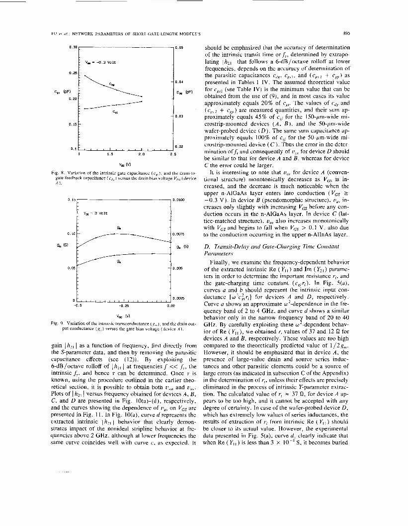
The drain bias dependence of the two important capac- itance parameters, namely, cgl and cdg, is presented in Fig. 8. It is evident from these curves that as the drain bias attains its saturation value, cg, attains its maximum value; whereas cdg attains its minimum value. This behavior is the consequence of the formation of a fixed carrier veloc- ity saturated region beyond L, that we have designated as LRd. The main reason for a fixed value of Lgd is the pres- ence of the n+ capping layer that defines this lateral ex- tension of the gate-to-drain depletion region of the partic- ular device investigated. The variations of the intrinsic transconductance (g,), and the output conductance ( g o ) with the gate bias voltage are depicted in Fig. 9. The shape of the variation of g, versus VGs curve indicates that, when VGs is increased above -0.3 V , g, begins to fall as a result of the n-AlGaAs layer entering into its conduction state. The output conductance ( g o ) monotonically in- creases with VGs, as can be expected, due to the move- ment of the operating point towards the “knee” of the IDS/ VDs curve.
C. The Current-Gain and Transit-Time Parameters As identified earlier, the key parameters of the intrinsic
FET equivalent network model that directly relate to the carrier transport mechanism are: cgI , g,,, (or 7 = cq , /gIn) , r,, and the phase delay time constant of Y2 , or the carrier transit delay time ( T,,). Before examining the last two pa- rameters (which are difficult to extract accurately, due to possible errors involved in removing the parasitic effects, as identified in subsection C of the Appendix, and possi- ble reference phase plane errors in the measurement of S-parameters), we will examine the transit time parameter (7) by plotting the magnitude of the short-circuit current
FU et al. : NETWORK PARAMETERS OF SHORT-GATE-LENGTH MODFET'S 895
- A
9. 0.05 - -
0 1 , , , , , , , , 1 , , , , , , , , ,
0'30:0'05 v, - -0.3 V o l t
90 (SI
0.005
0.0025
0.15
0 . 1 0.02
1 1.5 2.0 2.5
Vm M Fig. 8. Variation of the intrinsic gate capacitance ( c y , ) , and the drain-to-
gate feedback capacitance ( cdR) versus the drain bias voltage VDs (device A ) .
0.151 I0.0100
v, = 2 V o l t I
Vm (VI
Fig. 9. Variation of the intrinsic transconductance (g,,,), and the drain out- put conductance ( g , ) versus the gate bias voltage (device A ) .
gain lh2, I as a function of frequency, first directly from the S-parameter data, and then by removing the parasitic capacitance effects (see (12)). By exploiting the 6-dB/octave rolloff of I h,, 1 at frequencies f << f,, the intrinsic f,, and hence T can be determined. Once T is known, using the procedure outlined in the earlier theo- retical section, it is possible to obtain both U , , ~ and U,". Plots of 1 h2,I versus frequency obtained for devices A , B , C, and D are presented in Fig. 10(a)-(d), respectively, and the curves showing the dependence of U,, on VGs are presented in Fig. 11. In Fig. 10(a), curve d represents the extracted intrinsic 1 h,, 1 behavior that clearly demon- strates impact of the nonideal stripline behavior at fre- quencies above 2 GHz, although at lower frequencies the same curve coincides well with curve e , as expected. It
should be emphasized that the accuracy of determination of the intrinsic transit time orf7, determined by extrapo- lating Ih2, I that follows a 6-dB/octave rolloff at lower frequencies, depends on the accuracy of determination of the parasitic capacitances cdR, cRAl, and (eRF2 + c R p ) as presented in Tables I-IV. The assumed theoretical value for cRFl (see Table IV) is the minimum value that can be obtained from the use of (9), and in most cases its value approximately equals 20% of cR,. The values of cdR and ( cgJ + cRp) are measured quantities, and their sum ap- proximately equals 45% of cR, for the 150-pm-wide mi- crostrip-mounted devices ( A , B ) , and the 50-pm-wide wafer-probed device ( D ) . The same sum capacitance ap- proximately equals 100% of cqr for the 50-pm-wide mi- crostrip-mounted device ( C ), Thus the error in the deter- mination off, and consequently of U,, for device D should be similar to that for device A and B , whereas for device C the error could be larger.
It is interesting to note that U,, for device A (conven- tional structure) monotonically decreases as VGs is in- creased, and the decrease is much noticeable when the upper n-AlGaAs layer enters into conduction (VGs 1 -0.3 V ) . In device B (pseudomorphic structure), U,, in- creases only slightly with increasing VGs before any con- duction occurs in the n-AlGaAs layer. In device C (lat- tice-matched structure), ua, also increases monotonically with VGs and begins to fall when VGs > 0.1 V, also due to the conduction occurring in the upper n-AlInAs layer.
D. Transit-Delay and Gate-Charging Time Constant Parameters
Finally, we examine the frequency-dependent behavior of the extracted intrinsic Re ( Y,,) and Im ( Y2 , ) parame- ters in order to determine the important resistance r,, and the gate-charging time constant (c,,r,). In Fig. 5(a), curves a and b should represent the intrinsic input con- ductance [ w 2 c ~ , r , ] for devices A and D , respectively. Curve a shows an approximate @*-dependence in the fre- quency band of 2 to 4 GHz, and curve d shows a similar behavior only in the narrow frequency band of 20 to 40 GHz. By carefully exploiting these 0 *-dependent behav- ior of Re (Y,,), we obtained r, values of 37 and 12 Q for devices A and B , respectively. These values are too high compared to the theoretically predicted value of 1 /2g,. However, it should be emphasized that in device A , the presence of large-value drain and source series induc- tances and other parasitic elements could be a source of large errors (as indicated in subsection C of the Appendix) in the determination of r,, unless their effects are precisely eliminated in the process of intrinsic Y-parameter extrac- tion. The calculated value of r, = 37 Q , for device A ap- pears to be too high, and it cannot be accepted with any degree of certainty. In case of the wafer-probed device D , which has extremely low values of series inductances, the results of extraction of r, from intrinsic Re ( Y , , ) should be closer to its actual value. However, the experimental data presented in Fig. 5(a), curve d , clearly indicate that when Re ( Yl ) is less than 3 x lop4 S, it becomes buried
896
LEV. B -
v, = 0.2 volt
v, = 2.0 v o l t -
20 -
IEEE TRANSACTIONS ON ELECTRON DEVICES. VOL. 37. NO. 4. APRIL 1990
0.1 1 10 100
Frequency (GHz)
(a)
h,, (db)
0.1 0.3 1 3 10 30 100
Frequency (GHd
(c)
Fig. 10. (a) Frequency dependence of the current gain magnitude (hz l 1 (device A ) : curve cr-as measured. curve h-aftcr removal of parasitic gate capacitances, curve c-after removal of both parasitic gate capacitance and feedback capacitance. and curve d-extracted h z l . (b) Frequency dependence of the current gain magnitude 1 h 2 , I (device B ) : curve (r-as measured. curve b-after removal of parasitic gate capacitances, curve c-after removal of both paraaitic gate capacitance and feedback capacitance. (c) Frequency dependence of the current gain magnitude 1 /7,, 1 (device C ): curve a--as measured. curve h- after removal of parasitic gate capacitances, curve c-after removal of both paraaitic gate capacitance and feedback capaci- tance. (d) Frequency dependence of the current gain magnitude 1 h l l 1 (device D ) : curve tr-as measured. and curve /)--alter removal of both parasitic gate capacitance and feedback capacitance.
in the background noise level of the measurement system, and hence r, could not be extracted with any acceptable measure of accuracy. We have obtained Y, = 12 Q by drawing a w '-dependent straight line coinciding with the upper part of curve d within the 20- to 40-GHz frequency band. The nature of variation of Re ( Y , , ) data for the entire frequency band involved indicates that the accuracy of Y, determined in this case is also quite uncertain. Dam- brine et al . [ 161 also mentioned that the background sys- tem noise makes its determination difficult. Although they did not present Re ( Y I I ) versus frequency data graphi-
cally, they suggested that the inaccuracy could be as high as 50% without further explanation.
To see whether any significant contributions to the Re ( Y , , ) arising due to gate losses inherent in a passive- mode-operated device, we compare Re ( Y , , ) data ob- tained from both active- and passive-mode-operated de- vices as presented in Fig. 5(b). It follows from the large difference between curves b and c, and curves d and e , that the passive device contribution to Re ( Y , I ) is indeed negligible.
In Fig. 12, we observe a clear linear frequency depen-
FU CI ol. : NETWORK PARAMETERS OF SHORT-GATE-LENGTH MODFET‘S 897
Dev . c 0 I Dev . c 0 U
U k v . B
P 3 -
cev. A
o t , , , , I , , , ,
-0.6 -0.i 0.4
v, [v)
Fig. 1 I . Dependence of average carrier velocity ( z t a , ) on gate bias voltage for devices A , B , C, and D .
TABLE I ELECTRICAL PARAMETERS OF DEVICES A A N D D
dence behavior of Im ( Y z , ) extending over a wide range of frequencies for both devices A and B . After allowing for the drain-to-gate feedback capacitance ( cdx) from curves b and d , we obtain the “apparent” capacitance cil [ -1m Y 2 , / w ] , and the related “apparent” carrier transit delay time [ TA = ~ i ~ / g , ~ ] . Because of the low-fre- quency ( f << f7) approximation, T A also includes the gate-charging time constant [see subsection A of the Ap- pendix, (Ag)]. After subtracting 7 from T;, we can obtain ( cggr i - 0 . 6 ~ ~ ) . Thus either by neglecting T~ or using its
0 . 1 1 10 100
Frequency (GHz)
Fig. 12. Frequency dependence of intrinsic Im ( Y ? , ) : curve a-as mea- sured, and curve b-after correction for parasitic elements (device A ) , curve c-as measured, and curve d-after allowing for parasitic elements (device D ) .
cpi (PF) 23.6 33.1 42.1 47.9 57.9 cdg (fF) 12 13 13 15 13 &ll (4 24.3 37.4 49.9 58.2 62.2 J:‘ ( G H 4 164 180 189 193 171 J T (GHz) 154 168 176 179 160 u..t (10’ cm/sec) 3.27 3.56 3.73 3.80 3.40 wav (10’ cmisec) 2.73 2.98 3.12 3.17 2.83 h ( c a l c . ) (mS) 30.7 48.2 61.0 70.0 67.2
TABLE IV PARASITIC ELEMENTS
Dev.A Dev.B Dev.C Dev.D
150 0.9 3.5 3.7 0.33 0.43 0.045 0.027 0.060 0.032
150 0.9 3.4 2.4 0.3 0.42 0.043 0.027 0.042 0.042
50 1.2 7.0 6.4 0.3 0.36 0.045 0.009 0.028 -
50 2.0 10.5 8.0 0.001 0.0014 0.0043 0.009 0.010 -
estimated value, we obtain cgjr i , and hence ri. The results obtained for devices A and D based on the Y-parameter data presented above are compared below:
r, ( Q )
Device 7 ( p s ) C ~ I (fF) 7:, (ps) Im ( Y 2 1 ) Re ( Y , , ) Theory
A 1.67 446 4.16 13.9 37 4.1 D 0.525 81.9 0.979 10 12 6.0
898 IEEE TRANSACTIONS ON ELECTRON DEVICES. VOL. 37, NO. 4, APRIL 1990
It is clear from the above that the “apparent” value of the carrier transit delay ( T:) is greater than its theoretical upper limit of 1.57, in both cases. This has occurred, in the first place, most likely due to the presence of large series inductances, the effect of which could not be elim- inated accurately, in the case of device A , and secondly, due to possible reference plane phase errors in the mea- surement of the S-parameters. In the case of device D , the ratio of T ; / T is only moderately greater than 1.5, and this reflects that in this case, only small errors may have been introduced by the same factors identified above. As the wafer-probed S-parameter measurement technique im- proves, we hope that the accuracy in the determination of Im ( ) and Re ( Yl I ) will improve, and as a result, we should be able to accurately determine T A and ri in differ- ent MODFET structures, and better understand the dif- ference in their carrier transport dynamics at high fre- quencies.
For the purpose of ready reference and comparison, the results of determination of the equivalent network param- eters for the various devices tested are compiled and pre- sented in Tables I-IV.
111. CONCLUSIONS For the determination of equivalent network parameters
of millimeter-wave MODFET’s, a method of successive Y- to Z- and 2- to Y-conversion technique has been imple- mented utilizing the S-parameter data obtained from pas- sive and active mode operations of the same device. By using this technique, and a low-frequency assymptotic ap- proach, it has been possible to determine the intrinsic Re ( Y21) and Im ( YI1) parameters with a high degree of ac- curacy, and these parameters are essential in the extrac- tion of the intrinsic carrier transit ( T ) , and the related car- rier average velocity ( uav). However, an accurate determination of the intrinsic Im ( Y21 ), and Re ( Yl I ) pa- rameters by the same technique is not possible. This lim- itation arises partly due to a large impact of the device parasitic network elements (even in the case of wafer- probe measurements) on the measured Im ( U,, ), and Re ( YII) parameters, and partly due to the sensitivity limi- tations of the S-parameters measurements. This makes the determination of the intrinsic Im ( Y21 ) and Re ( Y1 ) highly prone to errors and it becomes difficult to extract the in- trinsic carrier transit delay ( T ~ ) and the gate charging time constant ( cg, r , ) , with acceptable accuracies. The results presented here demonstrate that devices mounted on a mi- crostrip test fixture suffers the most from these errors, and the errors in the case of wafer-probed devices are not to- tally eliminated either. It is believed, that with the im- provement of the wafer-probe measurement technique, the phase errors in the determination of Im ( Y21) and the in- ductive parasitic effects on both Im ( Y21) and Re ( Yl1) can be greatly reduced, and thus the accuracy in the de- termination of T~ and ( cg, r , ) can be significantly en- hanced. Without accurate determination of these time constants, no improvement in our understanding of the
dynamics of the velocity saturated carrier transport in MODFET’s involving different heterostructure designs can be achieved.
APPENDIX A . Dynamics of Velocity-Saturuted Currier Trunsport
In an earlier publication [26], the MODFET channel charge distribution, under current saturation mode of op- eration, was divided into two parts: a) the carrier-velocity nonsaturated charge, and b) the carrier-velocity saturated charge, consistent with the charge control model. Part a) was analyzed in the form of a distributed RC network, and part b) was treated as a constant-charge RC-network sup- ported by distributed constant voltage generators across the capacitance elements as depicted in Fig. 13. At high frequencies, even though these constant voltage genera- tors maintain their magnitude constant, a frequency-de- pendent phase delay is introduced as shown below.
It was shown in [26] that
From the representation of part b) we can express the elemental carrier charge and current due to carrier satu- ration velocity in the following manner: .
A Q = Z C ~ A X V
i ( x ) = ZCgVUsat
According to the continuity equation
For sinusoidal signals, replacing d /a t b y j o in (A3) and integrating from 0 to x, we obtain, for the voltage across the capacitance elements
(A41 I/ = voe - / l J ( r / k l , )
Using this V, the gate current ( ig2) can be written as L , + L,,,
i R 2 = j u z c o s Vdw. (A51
From the above equations we obtain
FU ('I ( I / NETWORK PARAMETERS O F SHORT-GATE-LENGTH MODFET'S
Y "g
(h) 47 l6= li(l-71
Fig. 13. Common-gate distributed RC-network representation of the MODFET. (a) Carrier velocity nonsaturated charge. (b) Carrier velocity saturated charge.
(A71
where I9 = ( 1 + 0 . 8 ~ ~ ) / ~ , / ) . Thus the intrinsic equivalent network of the active de-
vice can be represented in the manner shown in Fig. 14. Note that in (A7) we have introduced the factor 1 /( 1
+ jwcRi2r i2) in the Y2,-parameter. This was not consid- ered in obtaining (la). This has been done to approximate the distributed voltage ( V ) across the distributed capaci- tance elements of part b) distributed network representing the velocity-saturated charge, by an effective constant voltage z',? across cR12 and ri2 as shown in Fig. 14. At frequencies when wc,,r, << 1 , the imaginary part of Y2, and the real part of Y I I from (A7), respectively, can be approximated as
Im ( Y.,) = -wg,,,(O.47,) + T,/ + c Y , ? r j 2 )
Re ( Y l l ) = w-c;iIr,I + wzc$2r i2 . (A81 3 7
From the determination of the intrinsicf,, we have al- ready known 7 = ( T ~ ) + T ( / ) . When T~ << T ( / , as would be the case for devices with L,q I 0.25 pm, both r i I and cgi I can be ignored, and it becomes possible to determine the gate charging time constant ( cPi r , ) , directly from Im ( Y,l) after allowing for 7,/. Thus r i follows from the knowledge of c , ~ ~ . Alternately, ri can be obtained from the intrinsic Re ( Y, I ), since ( w cg i ) is already known.
B. The Efects of Microstripline Dispersion on Extructed Intrinsic Parameters dire to De-einheddirig
Consider an intrinsic FET structure with three parasitic series impedance elements (resistance and inductance), elements associated with its gate (Z?) , drain (Z(/), and source ( Z , ) terminals, and two shunt parasitic admittance elements (mostly capacitance) between the gate pad and the grounded source (Y?,?) and the drain pad and the
Fig. 14. Equivalent network representation of the intrinsic MODFET in common-source configuration showing the input and transfer admit- tances.
grounded source ( Y(/p). For simplicity, we assume that the nonideal 50 D behavior is caused by the dispersion effect in the microstrip lines which can be represented by a frequency-dependent function G ( f ). (In reality, there is possibility of discontinuity in the coaxial-to-microstrip transition as well.) - Thus the measured overall admittance parameters
( Yi l , etc. ) as modified by G ( f ) can be related to the Y-parameters ( Yi l , etc. ) in the absence of dispersion in the microstrip lines, in the following manner:
[FI = G ( f ) [ Y f I
A F = C ' ( f ) A Y ' (A9)
and
where A A = a l l a 2 2 - 4 2 1 4 1 2 .
In order to extract the intrinsic Y-parameters of the FET, one needs to first perform the S- to Y-transformation and allow for the shunt parasitic elements YR,, and Y+. Then convert the resultant Y-parameters to Z-parameters, allow for the series parasitic elements (Z,, Zd, and Z , ) , and fi- nally convert the resultant Z-parameter to Y-parameters which are the desired intrinsic Y-parameters. These trans- formations yielded the following expressions for Y, I and Y21:
(A10) 1 G ( f ) Y i l - YKP - A m +
G ( f ) Y i I - ygp - AP'(Z, + Zd)
A PAZ' YII =
Y2I = A PA.?? where
- - AP = A F - (Y,,Y& + Y + Y i l ) + Y?,,K,,,
= 21 21 - 21 21 1 1 2 2 21 12
I
Z' = . ( A l l ) G ( f ) Y h - U,, - A P ( z , + ZR)
AP
C. The Efects of Series Inductances ot i Re (Y, I ) and Iin
The effects of the presence of a source impedance Z, = ( r , + j w l , ) on the Y l l - and Y2,-parameters of an active device can be expressed in the following manner, when the intrinsic Y-parameters are designated as Y, ,,, Yzl , , Y2?,.
(Y2l)
900 IEEE TRANSACTIONS ON ELECTRON DEVICES, VOL 37. NO 4. APRIL 1990
and Y l z r = 0: (41 G. W. Wang, Y . K. Chen. W. J . Schaff. and L. F. Eastnian. "A 0.1 pin gate AIInAs/GaInAs MODFET fabricated on GaAs substrate." IEEE Trcrris. Elcwrori Devices. vol. 35. pp. 818-823. 1988.
IS ] R . L. Vaitkus, "Uncertainty in the values of GaAs MESFET equi+ alent circuit elements extracted from measured two-port scattering pa- rameters," presented at 1983 IEEE Cornell Cont. on High Speed Semiconductor Devices and Circuit\. Cornell Univ. Ithaca. NY. 1983.
161 W . R . Curtice and R. L. Camisa. "Self-consistent GaAs FET Models for amplifier design and device diagnostics," IEEE Trctris. Micro- i ~ ~ r i v Theory Tech.. vol. MTT-32, pp. 1573-1578. 1984.
171 W . R . Curtice. "The performance of submicrometer gate length GaAs MESFET's," 1EEE Trtiris. Elecrrori DciYc~es. vol. ED-30. pp. 1603- 1699. 1983.
YI I , Ytt =
1 + ( Y ~ l r + Ytti) ( 1 +;lliz.)]. (AI21
Y2ti
1 + (Yzti + Y,ti + Yz,i)Z, U21 =
By introducing a drain-to-gate feedback capacitance ( c d g ) , and gate and drain series impedances, Zg = rS + jwl,y, and Z, = rd + jwld, respectively (see Fig. I ) , we can express the Re ( Y , I ) and Im ( Y,, ) in the form of following approximate expressions when f << f T and g m >> go:
where c , ~ follows from Im ( Y z t ) / w as given in (A8), the various dashed parameters represent their undashed val- ues devided by the factor ( 1 + gmr,,). These equations clearly indicate how the parasitic elements influence Re ( Y, I ) and Im ( Y21 ) of a practical MODFET structure, par- ticularly when the series inductances f, and f,, are signifi- cant as in stripline-carrier-mounted samples.
ACKNOWLEDGMENT The authors wish to thank Dr. P. C. Chao, Dr. J . M.
Ballingall, and Dr. K.-H. G. Duh, Electronics Labora- tory, General Electric Company, Syracuse, NY, for val- uable discussions and for supplying the test devices.
I l l
1-21
131
REFERENCES T. Henderson. M. Aksun. C . Peng, H. Morkoc, P. C. Chao. P. M. Smith. K . Duh, and L. Lester. "Microwave performance of quartcr- micron gate low-noise pseudomorphic InGaAs/AIGaAs modulation- doped field-etfect transistor." 1EEE Electrofi DeiYce L m . . v o l .
P. Chao, R. C . Tiberio. K . H. G . Duh. P. M. Smith, J . Ballingal. L. F. Lester, B. R . Lee. A. Jabra. and G. Gifford. "0.1 pm gate- length pseudomorphic HEMT's." IEEE Electron De\,icc, LLJtf. . vol.
U. K. Mishra, A. S. Brown, L. M. Jelloian, L. H. Hackett. and M. J . Delaney. "High performance submicrometer AllnAs-GalnAs HEMT's." lEEE Elecvori Device Lett.. vol. 9. pp. 41-43, 1988. (Also see P. R . de la Houssayc. D. R . Allee. Y. C. Pao. D. G. Schloni. J . S. Harris. Jr . , and R. F. W. Pease. "Electron saturation velocity variatio? in InGaAs and GaAs channel MOSFET's for gate lengths of 550 A." IEEE Elecrrori Dc1.ic.r Letr.. vol. EDL-7. pp. 148-150. 1986.)
EDL-7, pp. 649-651, 1986.
EDL-8. pp. 489-491. 1987.
[SI L. Dearden cr U/. . "Model-extracted S-parameter design of MM-wave GaAs FET amplifiers," in 1986 MTT-S Dig. . pp. 385-388. 1986.
(91 A. K . Ketterson et u l . . "Characterization of InGaAs/AIGaAs pseu- domorphic modulation-doped field-cffect transistors." IEEE Trcrric. Electrori Devices. vol. ED-33. pp. 564-571, 1986.
[ I O ] G. I . Ng P I trl. . "Characteristics of strained In,, ,&a,, ,,As/ In,, ??AI,, 4xAs HEMT with optimized transport parameters." IEEE Elpctrorr Dei,icr. Len.. vol. 9. pp. 439-441. 1988. (Also see G . 1. Ng (,I U/. , "Improved strained HEMT characteristics u\ ing double-het- erojunction In,, ,&a,, 35As/lnf, F2AI,) ,hAs design," IEEE Elec.frori D e v i w Left . . vol. I O . pp. 114-1 16. 1989.
[ 1 I ] D. Arnold P I NI.. "Bias dependence of capacitances in modulation- doped FET's at 4 GHz." IEEE Electrorr Device Lrtt. . vol. EDL-5. pp. 123-125. 1984. (Also see D. Arnold ('I NI.. "Microwave char- acterimtion of AIGaAs/GaAs modulation-doped FET's: Bias depen- dence of small-signal parameters," IEEE Trtrris. E l c ~ r r o r i Dei.ic.es. v o l . ED-31. pp. 1399-1402, 1984.
[ 121 H. Hida ct til.. "A new low-noise AIGaAs/GaAs ZDEG FET with a surface undoped layer." IEEE Trciris. Electrori D<,i.ic,cc. vol. ED-33. pp. 601-607, 1986.
[I31 P. R . Jay ef al.. "Design of TEGFET devices for optimum low-noise high-frequency operation," IEEE Trtrris. EIec t ro~ Dci?cc..i. vol. ED-33, pp. 590-594. 1986.
I 141 T. Henderson er r r l . . "Microwave performance of a quartcr-microm- eter gate low-noise pseudomorphic InGaAs/AIGaAs inodulation- doped field effect transistor.'' /E€€ Elec.rrori Det.ic.r Le / / . . ~ 1 .
1151 L. D. Nguyen et al.. "Charge control, dc and RF performance of a 0 .35 pin pseudomorphic AICaAs/lnCaAs modulation-doped tield-el- fect transistor," IEEE Trcrrrs. Electrorr De\.ices. vol. 35. pp. 139- 144, 1988.
1161 G. Dambrine, A. Cappy. F. Heliodore. and E. Playez, "A new method for determining the FET small-signal equivalent circuit," 1EEE Trtrris. Micnjivrrw Theory T ~ I . . vol. 36, pp. 1151-1 159. 1988.
1171 A. van der Ziel and J. W. Ero. "Small-signal high-frequency theory of field-etfect transistors." IEEE Trrrris. Elrcrrori Do?c.c,.\. vol. ED-] I . pp. 128-135. 1964.
I 181 J . A. Geurst. "Calculations of high frequency characteristics of field- effect transistors." SoIi~I-Sratc Electrori. . vol. 8. pp. 563-566. 1965.
[ 191 B. Reddy and F. N . Trofimenkoff. "FET high-frequency analysis." Proc. f u . v / . Elrc. Erig. (London), vol. 113. pp. 1755-1762, 1966.
1201 M. B . Das. "Generalized high-frequency network theory of field-ef- fect transistors." Proc. 1ti.v. EIrc. Eri,q. (London). vol. 114. pp. 50- 59, 1967.
[2 I ] P. Wolf. "Microwave properties of Schottky-harrier field-eflect tran- sistors," IBM J . Res. Dei,.. vol. 14. pp. 125-141. 1970.
[ 2 2 ] M. B . Daj and P. Schmidt. "High-frequency limitations of abrupt- junction FET's." lEEE Trcrris. Elrctrnri Devic.es. vol. ED-20. pp. 779-792. 1973.
1231 H. Statz. H. Haus. a n d R. A . Pucel. "Noise characteristic5 of GaAs field-effect transistors," IEEE Trciri.5. Elrctrori Devic.os. vol . ED-2 I . pp. 549-562. 1974.
(241 C. A. Liechti. "Microwave field-etfect tranjistors." IEEE Trcurs. M i - croirai 'c Theory Tech. , vol. MTT-24. pp. 279-300, 1976.
1251 M. B . Das. "A high aspect ratio design approach to millimeter-wave HEMT's." 1EEE Trcrris. Elrc.troii Dei,ice.\. vol. ED-32, pp. 11-17. 1985.
1261 -. "Millimeter-wave performance of ultrasubmicroineter-sate field- etfect transistors: A comparison of MODFET. MESFET. and PBT structures." 1EEE Trurr,\. Elrcrrori DeiYws. vol. ED-34. pp. 1429- 1440, 1987.
1271 G. F. Ensen and C. A . Hoer. "'Thru-RcHect-l-inc': An improved
EDL-7, pp. 649-65 I . 1986.
FU et 611 . : NETWORK PAKAMETEKS OF SHORT-GATE-LENGTH MODFET‘S 90 1
technique for calibrating the dual six-port ANA.” IEEE Truns. Mi- croumv, Theor! Tech., vol. MTT-27. pp. 987-993. Dec. 1979.
1281 R. A. Speciale. “A generalization of the TSD network analyzer cal- ibration procedure, covering n-port scattering parameter nieasure- menta. affected by leakage errors,” IEEE Trm.s. Microivccw Tlieor! Tech.. vol. MTT-25, pp. 1100-11 15, Dec. 1977.
[29] T . H. Chen and M. S. Shur, “A capacitance model for GaAs MES- FET’s,” IEEE Truris. Elcwron Dei7ic~r.s. vol. ED-12. pp. 883-891. 1985.
1301 S. M. Liu, S. T . Fu, M. Thuruiraj. and M. B. Das. “Determination of source and drain series resistances in ultra-short gate-length MOD- FET’s,” IEEE Electron Device Lett . , vol. 10, pp. 85-87, 1989.
1311 P. C . Chao, S. C. Palmateer. P. M. Smith, U . K. Mishra. K.-H. G . Duh, and J . C. M. Hwang, “Millimeter-wave low-noise high elec- tron mobility transistors.” IEEE Truns. Elrctrori D r v i c m , vol. ED-33, pp. 531-533. 1986.
[32] W. J . Getsinger. “Microstrip dispersion model,” IEEE Trurzs. Mi- crmvuvt Theory T d z . . vol. MTT-2 l. pp. 34-39. Jan. 1973
*
Shih-Tsang Fu (S‘86) was born in Kaohsiung. Taiwan, on May 27, 1960. He received the B.S.E.E. degree from National Cheng Kung Uni- versity. Tainan. Taiwan. in 1982. and the M.S.E.E. from the Pennsylvania State Univer- sity, University Park. in 1986. He is currently working towards the Ph.D. degree in the Depan- ment of Electrical Engineering and carrying-out his research at the Center for Electronic Material and Processing, the Pennsylvania State Univer- sity.
His doctoral research is concerned with experimental studies o f \ubmi- crometer gate-length modulation-doped field-effect transistor5 (MOD- FET’s) involving the characterization at low-frequencies and high-fre- quency device parameters at room temperature and in liquid nitrogen temperature. The HF characterization work is aimed at extracting the in- trinsic device limitations and establishing a physics-based equivalent net- work model of the MODFET‘s. He received a GE fellowship for the years 1987- 1989.
Mr. Fu is a member of Tau Beta Pi.
Shih-Ming J . Liu was born in Kuching. Malay- sia, on April 15. 1958. He received the B.S . de- gree from the National Taiwan University in 1980. and the M.S. as well as Ph.D. degree from the Pennsylvania State University, University Park. in 1984 and 1987, respectively: all in electrical enginccring.
In 1981. he was an Assistant Engineer at the Electronics Research Services Organization (ERSO). ITRI, Taiwan. where he was involved in d e v e h i n g CMOS SRAM. He is currently a De- . -
vice Engineer at the GE Electronics Laboratory in Syracuse, N Y , His re- search interests concern millimeter-wave characterization and application of heterostructured FET‘s.
*
Mukunda B. Das (S’S7-M‘62-SM’70) was born in Bagerhat, Bangladesh. on September I . 1931. He received the B.Sc. (honors). and M.Sc. de- grees in applied physics from Dhaka University. Dhaka, Bangladesh, in 1953 and 1955. respec- tively. the Diploma of the Imperial College of Science and Technology (DIC). London, UK, and the Ph.D. degree from the University of London, both in 1960.
From 1960 to 1962. he was a Lecturer in Elec- trical Engineering at the Imperial College. He
served as a Senior Scientific Offic’er at the East Regional Laboratories of the Council of Scientific and Industrial Research, Dhaka, from 1962 to 1964. In 1965. he joined ASM. Ltd.. G . E. C . Hirst Research Center. Wembley. Middlesex, England, and served as a Principal Scientific S t a f Member. and Leader of the MOS Integrated Circuits Group. In 1968, he joined the Pennsylvania State University, University Park, as an Associate Professor in Electrical Engineering. He became a Professor in 1979. and for the academic year 1983-1984 scrvcd as an IPA Visiting Professor at the Wright-Patterson AFB. Ohio. He spent the Fall of 1987 as a Visiting Professor in the Department of Radio and Space Science, Chalmers Uni- versity of Technology. Gothenburg. Sweden. He is Associate Director of the Center for Electronic Materials and Processing under the College of Engineering at Penn State. He has authored and coauthored over 75 pub- lications i n refereed scientific journals, and has been granted eight British and U.S. patents concerning the field-ctfcct device design and fabrication. His current reearch interests include HF limitations of devices. millime- ter-wave device design, and performance evaluation, including LF and HF noise behavior of GaAs MESFET’s. modulation-doped FET’s. HBT’s, and thin-oxidc-gate \illcon MOSFET‘s. He is also actively involved in char- acterization o f material defects in devices through electrical measurements. and understanding interrelationships between material and device charac- teristics. He is a recipient of the 1967 Blumlein-Browne-Willian Premium Award for his published work in the Proc,cedirig.s o f / / i c IEE (London).