Development of hyperspectral CL imaging systems for the characterization of semiconducting materials P.R. Edwards, K.J. Lethy, J. Bruckbauer, N. Kumar, M. Wallace, F. Luckert, F. Sweeney, C. Trager-Cowan, K.P. O’Donnell and R.W. Martin Department of Physics University of Strathclyde Glasgow, Scotland MAS Topical Conference Cathodoluminescence 2011
Transcript
Development of hyperspectral CL imaging systems for the characterization of
semiconducting materials
P.R. Edwards, K.J. Lethy, J. Bruckbauer, N. Kumar,M. Wallace, F. Luckert, F. Sweeney, C. Trager-Cowan,
K.P. O’Donnell and R.W. Martin
Department of Physics
University of Strathclyde
Glasgow, Scotland
MAS Topical ConferenceCathodoluminescence 2011
2
Talk outline• Introduction
– to our research group & nitride semiconductors
• CL hyperspectral imaging– what it is & why we need it
– optical design considerations
– combining with
• WDX
• electron diffraction techniques(EBSD/ECCI)
• Data analysis– peak fitting
– multivariate statistical analysis
• Where next?
all illustrated with examples from our work
2.90
2.85
2.80
2.75
eV
1 µm
0 200 400 600 800 1000
distance (nm)
0
200
400
600
800
dist
ance
(nm
)
2.95
3.00
3.05
3.10
3.15
centroid (eV)
100 nm
6 kV
100 nm
6 kV
0.0 0.1 0.2 0.3 0.4 0.5 0.6
distance (µm)
2.76
2.78
2.80
2.82
2.84
centre (eV)
2.54
2.56
2.58
2.60
centre (eV)
0.0 0.2 0.4 0.6 0.8 1.0Distance (inches)
3
Introduction
• Semiconductor Spectroscopy and Devices group– Interested in light-emitting semiconductor materials– Particular focus on group III nitrides: GaN, InN, AlN and their alloys– Spectroscopic characterization techniques include:
Field emission SEM arrives.CL hyperspectral imaging immediately added
CL hyperspectral imaging software evolves
We are here
5
Group III nitrides
AlN
GaN
InN
• Emission wavelength dependent on bandgap
• Band gap energies of: 6.2 eV (AlN)3.4 eV (GaN)0.7 eV (InN)
• Alloys (e.g. InxGa1-xN) can be tailored toemit across the visible region and beyond
• Extremely bright CL at room temperature
Lattice constant (Å)
3.0 3.2 3.4 3.6
Ban
dgap
ene
rgy
(eV
)
0
1
2
3
4
5
6
7
GaN
InN
AlN
White/blue
LEDs
Blue laser
diodes
6
Hyperspectral imaging
• “Hyperspectral image”– a.k.a. “spectrum image”, “spectral map” etc.– Term borrowed from remote sensing– 20+ contiguous wavelength bands
• Acquisition modes:– Image at a time
(e.g. using tuneable filter)– Line at a time
(“push broom” method)– Spectrum at a time
� Christen et al. J. Vac. Sci. Technol. B 9, 2358 (1991)
e-λ
I
λ
I
λ
I
x
y
λ
“Data cube”
7
Why hyperspectral imaging?• More data! • No need to choose particular points or wavelength bands
beforehand• The only way to map wavelength shifts
Among many other factors causing wavelength shifts are:-
• Composition• Temperature• Elastic strain• Carrier concentrations• Magnetic and electric fields• Measurement geometry
– Self-absorption– Optical modes
All lead to continuous variability in the band-gap energy
e-λ
Iλ
Iλ
I
x
y
λ
“Data
cube”
8
Moving peaks• Changing alloy fractions:
(e.g. x varies in InxGa1-xN)
λ
Compressive strain
Blue shift
Tensile strain
Red shift
Em
issi
on
Pure GaNIn0.4Ga0.6N
Photon Energy (eV)1.0 1.5 2.0 2.5 3.0 3.5Lo
w t
em
pe
ratu
re P
L E
mis
sio
n (
a.u
.)
• These shifts cannot be mapped using conventional CL (monochromatic images and point spectra) ⇒⇒⇒⇒ Need for CL HSI
• Elastic strain:
9
However, for any optical system these parameters are linked through the invariant quantity, étendue or Lagrange Invariant:
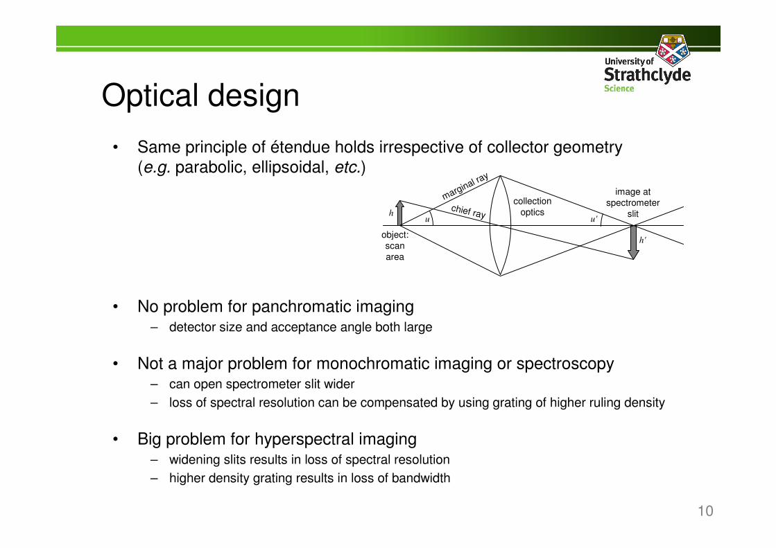
Optical design and “étendue”
• Some basics:– Aim to get light from sample to detector– Do this using some optical system:
u'uh
h'object: scan area
image at spectrometer
slitcollection
optics
marginal ray
chief ray
want angle u to be as large as possible for maximum collection
want image size h' to be small enough for detector entrance
want object hto be as large as possible for maximum field of view
want angle u' to be small enough to match detector f-number
nh sin u = n'h' sin u'
10
Optical design
• Same principle of étendue holds irrespective of collector geometry(e.g. parabolic, ellipsoidal, etc.)
• No problem for panchromatic imaging– detector size and acceptance angle both large
• Not a major problem for monochromatic imaging or spectroscopy– can open spectrometer slit wider– loss of spectral resolution can be compensated by using grating of higher ruling density
• Big problem for hyperspectral imaging– widening slits results in loss of spectral resolution– higher density grating results in loss of bandwidth
u'uh
h'object: scan area
image at spectrometer
slitcollection
optics
marginal ray
chief ray
11
Optical design
• Calculate FOV vs. collection– Assume Lambertian emission profile
(intensity varies as cosθ)– Integrate over collection cone:
• Some typical numbers:– f/4 spectrometer (i.e. a high
acceptance angle)– 25 µm slit (matched to 1"
CCD with 1000 pixels)
• 90% collection limits you to 1 µm FOV• 10 µm FOV limits you to 9% collection
emission angle θ
∫ ∫= =
==u
udd
0
22
0
sinsincoscollection
θ
π
φ
θφθθ
0.1 1 10 1000.0
0.2
0.4
0.6
0.8
1.0
Col
lect
ion
effic
ienc
y
Field of view (µm)
× 250 × 25 × 2.5 × 0.25
0.000
0.447
0.632
0.775
0.894
1.000
Optical magnification
Collection N
.A.
12
CL systems at Strathclyde
• We get around the FOV vs. collection problem by developing two CL systems:1. High resolution system based on FEI Sirion field emission SEM
(where large field of view not required)2. Large field of view system based on Cameca SX100 electron
microprobe (where the stage is scanned rather than the beam)
13
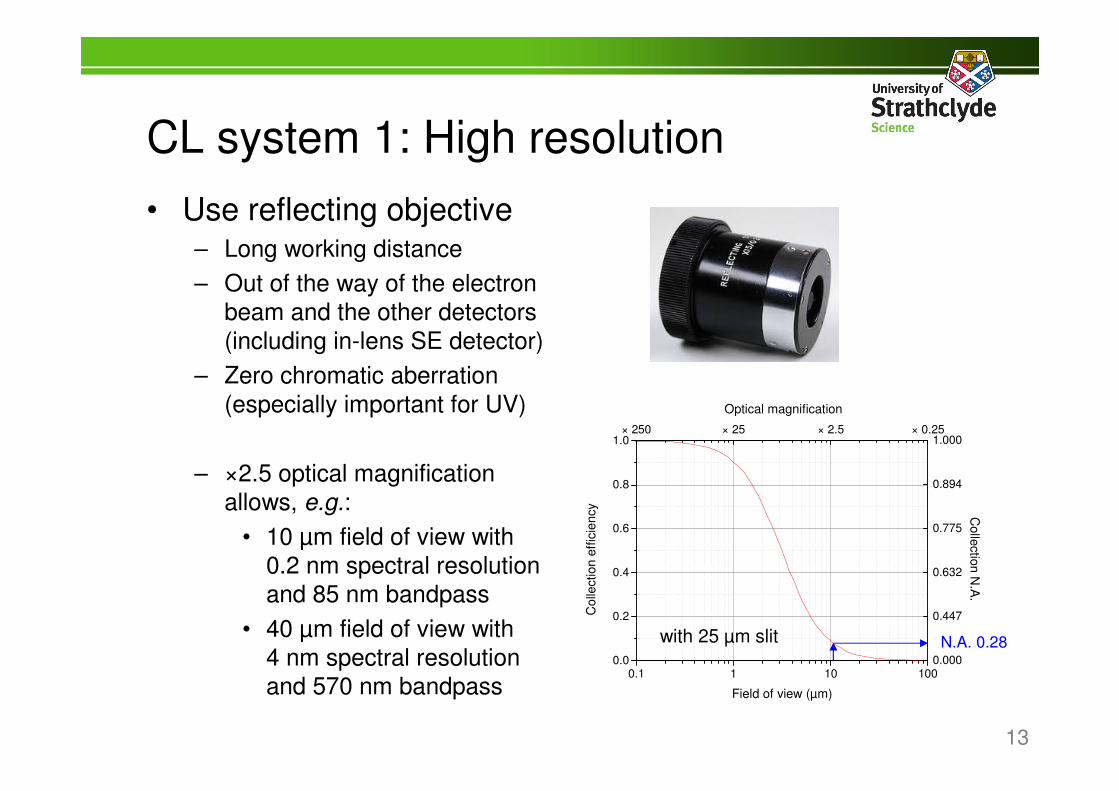
CL system 1: High resolution
0.1 1 10 1000.0
0.2
0.4
0.6
0.8
1.0
Col
lect
ion
effic
ienc
y
Field of view (µm)
× 250 × 25 × 2.5 × 0.25
0.000
0.447
0.632
0.775
0.894
1.000
Optical magnification
Collection N
.A.
N.A. 0.28
• Use reflecting objective– Long working distance – Out of the way of the electron
beam and the other detectors (including in-lens SE detector)
– Zero chromatic aberration (especially important for UV)
– ×2.5 optical magnification allows, e.g.:
• 10 µm field of view with 0.2 nm spectral resolution and 85 nm bandpass
• 40 µm field of view with 4 nm spectral resolution and 570 nm bandpass
with 25 µm slit
14
• Collection at 90°to the beam
• Sample tilted to ~45°
• All-reflecting design
• Electron multiplying CCD allows on-chip electron amplification for improved signal:noise
• 1 MHz readout – spectral acquisition times down to 2 ms
• Control and analysis using home-grown software package “CHIMP”
CL system 1: High resolution
NA 0.28 reflectingobjective
quartz vacuum window
parabolic mirror
spectrograph
tilted sample
EMCCD
e-beam
15
Collection geometry dependence
InGaN/GaNQW cavity
CL collection cone
Direct collection Collection through mirror
Eucentricsample rotation
45°angled
stub
e-beam
2.9 3 3.1 3.2 3.3 3.4 3.5
energy (eV)
CL
inte
nsity
(a.
u.)
direct collection
collectionthrough mirror
A B A B
λ
emission
absorption
Plan view, collection from above
Same spectrum at A and B
Tilted sample, collection from side
Light from A absorbed more than light from B
Can lead to apparent red shift
light collection
lightcollection
16
CL system 2: Large field of view• Uses built-in optical
microscope of Cameca SX100 to collect emission
• Output directly coupled to f/number-matched CCD spectrograph
• This gives optical magnification of ~×3
• EPMA controls scan (moving beam or stage)
• WDX acquisition unaffected
• Separate CL control synchronises spectrum acquisition – again using “CHIMP”
xyz scanning stage
1/8 mspectrograph
cooled CCD
electroncolumn
to WDX spectrometers
mirror
lens
optical reflecting objective
electron objective
PC
17
CL system 2
f/3.7spectrograph
cooled CCD
lens and folding mirror
Hg calibration lamp
WDX spectrometer
18
“CHIMP” software• Controls hyperspectral
image acquisition
• Allows analysis, e.g.– Individual or mean
spectra– Maps of intensity, peak
position, FWHM, real colour
– Linescans– Line spectra– Correlation plots– Multiple peak fitting– Principal component
analysis– Importing images files
(e.g. *.tif, Cameca *.img)
Cathodoluminescence Hyperspectral Imaging & Manipulation Program
19
Peak fitting• Typical acquisition times of 10’s of ms - spectra tend to be noisy
• Many emission peaks from semiconductors can be approximated by simple functions (e.g. Gaussian, Lorentzian, Voigt, Pekarian)
• We use a Levenberg-Marquardt non-linear least squares (NLLS) optimization algorithm to fit functions to each spectrum in the hyperspectral image
• This results in much reduced noise in images of peak intensity, wavelength, widths etc.
Pixel (138,191)
1.5 2.0 2.5 3.0 3.5
energy (eV)
0
500
1000
1500
corr
ecte
d si
gnal
(co
unts
) • Example of a 3-peak fit to a CL spectrum from a GaN/InGaN LED structure
• The fitting is repeated independently for each of the 1000s of spectra in the dataset
20
Wafer mapping using CL HSI
2.54
2.56
2.58
2.60
centre (eV)
0
2000
4000
6000
8000 height (counts)
125
130
135
140
145 FWH
M (m
eV)
0.0 0.2 0.4 0.6 0.8 1.0Distance (inches)
Peak energy Peak width Peak height
Pixel (138,191)
1.5 2.0 2.5 3.0 3.5
energy (eV)
0
500
1000
1500
corr
ecte
d si
gnal
(co
unts
)
2" diameter wafer
yellow band (defects)
InGaN/GaN quantum well
GaN near-band-edge
• GaN/InGaN blue LED structure• 100’s of 1mm2 LEDs with metal contacts• Focus here on the QW peak• Fitting allows it to be easily deconvolved
from overlapping defect band• Long-range variation could be due to
change in InGaN composition• No variation within each 1 mm2 LED
21
Electric field-induced peak shifts
GaN
InGaN
CB
VB
CB
VB
ener
gy
GaN Quantum well structure
Ideal band diagram- electron and hole wavefunctions overlap
In certain crystal directions, heterojunctions lead to polarization fields being induced- electron and hole wavefunctions separated- emission intensity reduced- red-shift in emission wavelength- compounded by piezoelectric field
“Quantum-Confined Stark Effect”
22
Effect of electric field E on CLBlue-shifted, narrower, lower intensity - correlates with higher SE signal
2.54
2.56
2.58
2.60
centre (eV)
CB
VB
CB
VB
energy
voltage
Higher SE signal implies lower (more negative) potential at surface
This results from injection of excess carriers into p-n junction
Open circuit, so results in p-type becoming more negative (c.f. photovoltaic effect)
Higher electric field counteracts QCSE (blue shift narrowing) but reduces radiative recombination
CL peak position Secondary electron signal
substratetop surface
top surface
substrate
small E large E
23
CL and WDX• The EPMA-based system allows CL hyperspectral imaging and WDX
mapping to be carried out simultaneously
• E.g. the quaternary alloy AlxInyGa1-x-yN
• Grown using MBE: complex interplay between elemental concentrations
� P.R. Edwards, R.W. Martin, et al. (2009) Superlattices and Microstructures 45, 151-155
incr
easi
ng T
24
Correlations
2-dimensional histograms
4 5 6 7 8 9
% InN
3.16
3.17
3.18
3.19
3.20
3.21
cent
re (
eV)
0
5
10
15
20
25
30
pixel frequency
Ga vs. In Al vs. In CL energy vs. InN fraction
Pearson product-moment correlation coefficients:+(-) 1: perfect +ve (-ve) linear correlation0: no linear correlation
-0.40 -0.08 -0.75
25
CL and EBSD
-0.006
-0.005
-0.004
-0.003
-0.002
-0.001
0
0.001
0.002
0.003
0 5 10 15 20 25
wingseed wing wingseed
distance (µm)
In plane strain
referencepoint
[1210]
3.413 eV
3.408 eV
• Previous work collaborating with Angus Wilkinson (University of Oxford)
• GaN sample with periodic strain variation
• Electron backscatter diffraction (EBSD) used to map strain tensor variation
• Good agreement with strain calculated from CL wavelength image (measured ex-situ)
• Our FE-SEM CL system has the geometry to allow electron diffraction and CL measurements simultaneously
26
CL and ECCI• Electron Channelling
Contrast Imaging(forescatter imaging)
• Contrast results from small changes in strain
• This occurs at threading dislocations (screw, edge, mixed) and also atomic steps
� C.Trager-Cowan et al. Phys. Rev. B 75 085301 (2007)
SEM pole piece
ECCI detectordiode
Channellingin electrons
Electrons out
27
CL/ECCI and defects• Apparent 1:1 correlation
between CL dark spots and ECCI spots
• These measurements will allow direct correlation between structural and optical properties (e.g. which dislocation types act as centres for non-radiative carrier recombination)
• Requires compromise between the contradictory demands of the two techniques: high kV for ECCI, low kV for CL
1 µm
ECCI
CL
28
Principal component analysis
The classic description in 2-D:
x
y
x'
y'
x'
y'
c1c2
Data varies in x and y Mean adjusted data Find new orthogonal axes, with most variance along first axis: this is first principal component
29
Principal component analysis
[ ] [ ] [ ]WH
RHWX
≈
+= mrrnmn ,,,
…
…
≈
m spatial data points
nsp
ectr
al c
hann
els
r spectram spatial data points
r images
m spatial data points
“scores” “loadings”original data
Principal components ranked in order of their contribution to the total data variance
Hyperspectral image now described not as sum of n monochromatic wavelengths, but as the sum of r (where r<m) spectra [See work by P. Kotula (Sandia) on EDX data]
original data
spectraimages
residual
30
PCA example: Eu-doped GaN• Example: Rare earth-doped semiconductors• Emission due to transitions within 4f shell of RE ions
– Largely independent of host material– Sharp emission lines with fixed spectral “signature”
• GaN implanted with Eu• Promising route to producing red LEDs from GaN
31
Eu-doped GaN
0 5 10 15 20
distance (mm)
0
1
2
3
4
5
6
dist
ance
(m
m)
400 500 600 700 800
w avelength (nm)
0
500
1000
1500
corr
ecte
d si
gnal
(co
unts
)
400 500 600 700 800
w avelength (nm)
0
500
1000
1500
2000
corr
ecte
d si
gnal
(co
unts
)
400 500 600 700 800
w avelength (nm)
0
20
40
60
corr
ecte
d si
gnal
(co
unts
)
Calculated “real” colour image from hyperspectral image (log scale)
Sample spectra: overlapping peaks, including Eu-related, GaN band edge and yellow band, and thickness fringes
32
PCA & overlapping peaksPCA results when taking first 6 components;
0 5 10 15 20
distance (mm)
0123456
dist
ance
(m
m)
0 5 10 15 20
distance (mm)
0123456
dist
ance
(m
m)
0 5 10 15 20
distance (mm)
0123456
dist
ance
(m
m)
0 5 10 15 20
distance (mm)
0123456
dist
ance
(m
m)
0 5 10 15 20
distance (mm)
0123456
dist
ance
(m
m)
0 5 10 15 20
distance (mm)
0123456
dist
ance
(m
m)
400 500 600 700 800
w avelength (nm)
-0.1
0.0
0.1
0.2
0.3
0.4
0.5
0.6
raw
sig
nal
(cou
nts)
400 500 600 700 800
w avelength (nm)
-0.02
0.00
0.02
0.04
0.06
0.08
0.10
0.12
raw
sig
nal
(cou
nts)
400 500 600 700 800
w avelength (nm)
0.0
0.1
0.2
0.3
0.4
0.5
raw
sig
nal
(cou
nts)
400 500 600 700 800
w avelength (nm)
-0.05
0.00
0.05
0.10
raw
sig
nal
(cou
nts)
400 500 600 700 800
w avelength (nm)
0.00
0.05
0.10
raw
sig
nal
(cou
nts)
400 500 600 700 800
w avelength (nm)
0.0
0.1
0.2
0.3
0.4
raw
sig
nal
(cou
nts)
33
0
200
400
600
800
1000
1200
1400
1600
1800
2000
3 3.5 4 4.5 5 5.5
Energy (eV)
CL
in
ten
sit
y
w urtzite
zincblende
PCA example with moving peaks
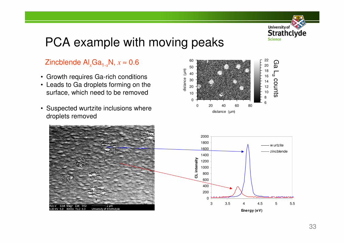
Zincblende AlxGa1-xN, x ≈ 0.6
• Growth requires Ga-rich conditions• Leads to Ga droplets forming on the
surface, which need to be removed
• Suspected wurtzite inclusions where droplets removed
0 20 40 60 80
distance (µm)
0
10
20
30
40
50
60
dist
ance
(µm
)
6810121416182022
(counts)G
aLα
counts
340 2 4 6 8 10
distance (µm)
0
2
4
6
8
10
dist
ance
(µm
)
3.803.853.903.954.004.054.104.15
CL energy (eV
)PCA example with moving peaks
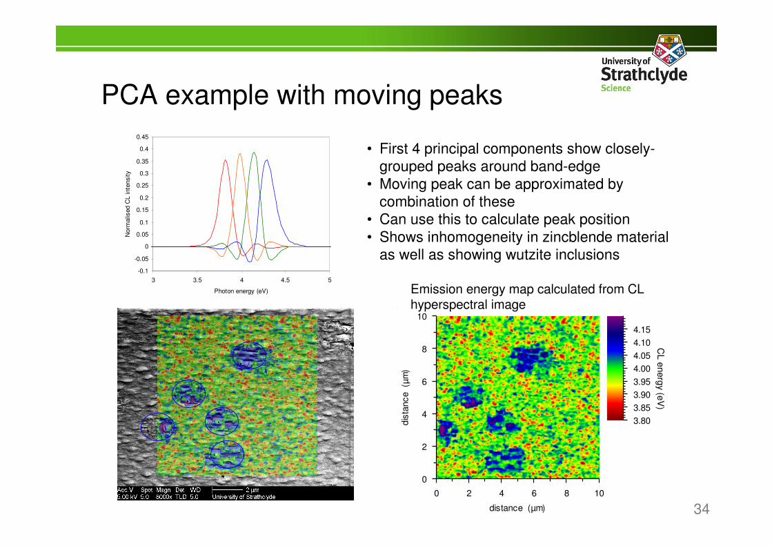
Emission energy map calculated from CL hyperspectral image
-0.1
-0.05
0
0.05
0.1
0.15
0.2
0.25
0.3
0.35
0.4
0.45
3 3.5 4 4.5 5
Photon energy (eV)
Nor
mal
ised
CL
inte
nsity
• First 4 principal components show closely-grouped peaks around band-edge
• Moving peak can be approximated by combination of these
• Can use this to calculate peak position• Shows inhomogeneity in zincblende material
as well as showing wutzite inclusions
35
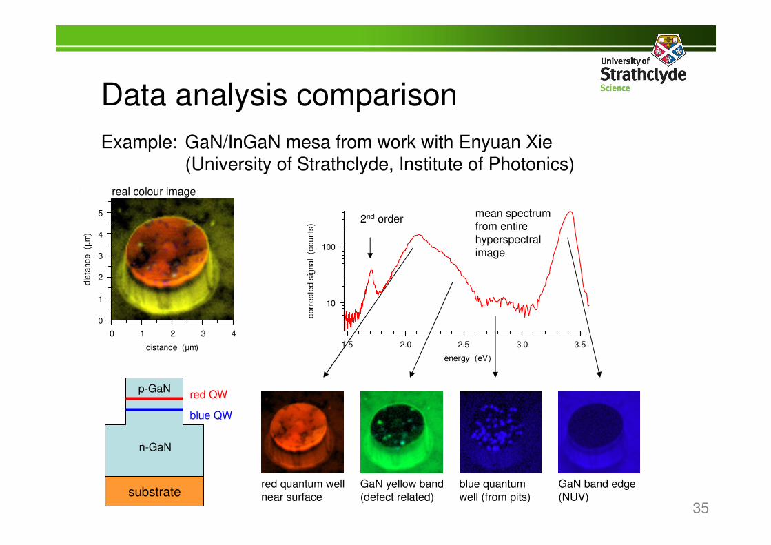
Data analysis comparisonExample: GaN/InGaN mesa from work with Enyuan Xie
(University of Strathclyde, Institute of Photonics)
0 1 2 3 4
distance (µm)
0
1
2
3
4
5
dist
ance
(µm
)
1.5 2.0 2.5 3.0 3.5
energy (eV)
10
100
corr
ecte
d si
gnal
(co
unts
)
p-GaN
2nd order
n-GaN
red QW
blue QW
red quantum well near surface
GaN yellow band (defect related)
blue quantum well (from pits)
GaN band edge (NUV)
mean spectrum from entire hyperspectral image
real colour image
substrate
36
Extracting wavelength images
0 1 2 3 4
distance (µm)
0
1
2
3
4
5
dist
ance
(µm
)
0 1 2 3 4
distance (µm)
3.32
3.34
3.36
3.38
3.40
3.42
0 1 2 3 4
distance (µm)
0
1
2
3
4
5
dist
ance
(µm
)
0 1 2 3 4
distance (µm)
3.32
3.34
3.36
3.38
3.40
3.42
Pixel (57,5)
1.5 2.0 2.5 3.0 3.5
energy (eV)
200
400
600
800
corr
ecte
d si
gnal
(co
unts
)
This is not “smoothing” – none of these images has lost any spatial resolution
Peak intensity – simply find point in spectrum with highest intensity
Centroid – find “centre of mass” of the spectrum
NLLS fitting of peak function (in this case Gaussian + LO phonon replicas)
Centroid of principal components (in this case the first 5 PCs)
19.01% of variance2nd component
1.5 2.0 2.5 3.0 3.5
energy (eV)
0.0
0.1
0.2
0.3
0.4
raw
sig
nal
(cou
nts) 46.79% of variance1st component
1.5 2.0 2.5 3.0 3.5
energy (eV)
0.0
0.1
0.2
0.3
0.4
raw
sig
nal
(cou
nts) 5.74% of variance4th component
1.5 2.0 2.5 3.0 3.5
energy (eV)
-0.05
0.00
0.05
0.10
0.15
raw
sig
nal
(cou
nts)
Focusing on the GaN near-band-edge emission:
37
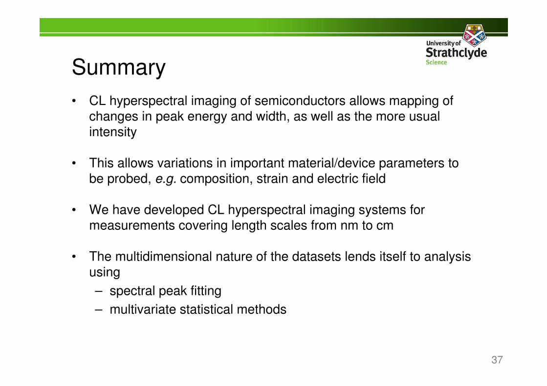
Summary• CL hyperspectral imaging of semiconductors allows mapping of
changes in peak energy and width, as well as the more usual intensity
• This allows variations in important material/device parameters to be probed, e.g. composition, strain and electric field
• We have developed CL hyperspectral imaging systems for measurements covering length scales from nm to cm
• The multidimensional nature of the datasets lends itself to analysis using– spectral peak fitting– multivariate statistical methods
38
Continuing work
• Simultaneous ECCI and CL imaging– Working to overcome the opposing requirements of the two techniques
• CL in variable-pressure SEM– Allowing CL measurement of less conductive materials (such as wider
bandgap semiconductors) without coating
• Integration of CL with electrical measurements– Bias-dependent CL to probe carrier dynamics within LED junctions
while maintaining high spatial resolution.– Electron Beam-Induced Current (EBIC) to complement the CL and
ECCI measurements on individual dislocations
• Keep pushing towards higher spatial resolution– See tomorrow’s talk…
39
Acknowledgments• Thanks to
– C. Liu, D. Allsopp, P. Shields and W. Wang (University of Bath)– T. Wang and co-workers (University of Sheffield)– R. Oliver and M. Kappers (University of Cambridge)– N. Grandjean (EPFL)– S. Fernandez-Garrido and E. Calleja (Universidad Politécnica de Madrid)– S. Novikov and T. Foxon (University of Nottingham)– E. Xie, E. Gu, I.M. Watson, and M.D. Dawson (University of Strathclyde,
Institute of Photonics)for providing samples.
• This research was supported by the UK Engineering and Physical Sciences Research Council.