DEVELOPMENT OF SILICON-ON-INSULATOR (SOI) TRAPEZOIDAL WAVEGUIDE USING ANISOTROPIC WET ETCHING KHAIRUL ANUWAR BIN ABU KASIM This Report Is Submitted In Partial Fulfillment of Requirements for the Bachelor Degree of Electronic Engineering (Computer Engineering) Fakulti Kejuruteraan Elektronik dan Kejuruteraan Komputer Universiti Teknikal Malaysia Melaka June 2015
Transcript
DEVELOPMENT OF SILICON-ON-INSULATOR (SOI) TRAPEZOIDAL
WAVEGUIDE USING ANISOTROPIC WET ETCHING
KHAIRUL ANUWAR BIN ABU KASIM
This Report Is Submitted In Partial Fulfillment of Requirements for the
Bachelor Degree of
Electronic Engineering (Computer Engineering)
Fakulti Kejuruteraan Elektronik dan Kejuruteraan Komputer
Universiti Teknikal Malaysia Melaka
June 2015
ii
DECLARATION
“I hereby declare that this report is the result of my own work with the exception of
the quotes as cites in the references.”
Signature :…………………………………………………
Name : KHAIRUL ANUWAR BIN ABU KASIM
Date : 2015
iii
APPROVAL
“I hereby declare that I have read this report and in my opinion this is enough in
terms of the scope and quality for the award of Bachelor of Electronic Engineering
(Computer Engineering) With Honors’.”
Signature :………………………………………
Supervisor’s Name : DR. HAZURA BINTI HAROON
Date : 2015
iv
Specially dedicate to my parents, my siblings and not to forget my friends and people around me who always supporting me through this whole times.
v
ACKNOWLEDGEMENT
Bismillahhirrahmannirrahim, praise to almighty God for giving me this
opportunity and ease to complete my project. First of all, I would like to take this
opportunity to express my greatest gratitude to project supervisor, Dr. Hazura Binti
Haroon for his guidance, encouragement and endurance during the whole process of
this project. It is indeed my pleasure to have him to support me with limitless
advices and enthusiastic spirit towards my project.
I also would like to offer my special thanks to my beloved family,
exclusively to both of my parents, Abu Kasim Bin Mohamed and Hanipah Binti
Ismail for their continuous support throughout the years of my study in University of
Technical Malaysia Malacca (UTeM). They are the main reason for the person that I
am becoming today, without their support, this project would not be completed
successfully.
Special thanks to all of my friends especially to my course mates for their
technical advices. Lastly, to all the people that involve with this project either
directly or indirectly, once again, thank you very much.
vi
ABSTRACT
Silicon-On-Insulator (SOI) is a unique and attractive technology for the chip
making process and it also give benefit in low power, low voltage and high speed
processing. This technology was introduced to the semiconductor production in year
1960 using the name of Silicon-On-Sapphire (SOS). In this project, the process of
modeling, optimization and characterization of Silicon-On-Insulator using Silvaco
software are proposed. The optimized silicon-On-Insulator trapezoidal waveguide
components are aimed to be implemented in future photonic devices such as planar
lightwave circuit. Both anisotropic wet etching and dry etching are considered to
evaluate the effect of etching techniques on the waveguide structure and for this
project anisotropic wet etching is used. In addition, the Taguchi methods are
employed to study the influence of fabrication parameters on fabrication
performance such as etch rate and waveguide structure. Four fabrication parameters
are considered includes phosphorus doping concentration, boron doping
concentration, phosphorus diffusion time and boron diffusion time. The study
involved both N-type and P-type waveguide structure with silicon orientation of
<100>. The Silicon-On-Insulator fabrication process has been done through their
level process with the use of Silvaco software and the optimization of the silicon
optical waveguide modulation efficiency has been analyzed with the parameters
value variation.
vii
ABSTRAK
Silicon-On-Insulator (SOI) adalah teknologi yang unik dan menarik untuk
proses membuat cip dan ia juga member manfaat dalam kuasa yang rendah, voltan
rendah dan pemprosesan kelajuan tinggi. Teknologi ini telah diperkenalkan kepada
pengeluaran semikonduktor pada tahun 1960 menggunakan nama Silicon-On-
Sapphire (SOS). Dalam projek ini, proses pemodelan, pengoptimuman dan pencirian
Silicon-On-Insulator menggunakan perisian Silvaco. Silicon-On-Insulator trapezoid
struktur ini dioptimunkan untuk kegunaan Planar Lightwave Circuit. Kedua-dua
punaran sama ada basah atau kering memberikan kesan yang tertentu kepada
Silicon-On-Insulator dan untuk projek ini punaranan isotropic basah digunakan. Di
samping itu, kaedah Taguchi digunakan untuk mengkaji pengaruh fabrikasi pada
parameter fabrikasi seperti prestasi kadar punaran dan struktur pandu gelombang.
Empat parameter fabrikasi yang dipilih ialah phosphorus doping concentration,
boron doping concentration, phosphorus diffusion time and boron diffusion time.
Kajian ini melibatkan kedua-dua jenis-N dan Jenis-P struktur silicon pandu
gelombang dengan orientasi <100>. Silicon-On-Insulator proses fabrikasi telah
dilakukan mengunakan perisian Silvaco dan pengoptimuman silicon pandu
gelombang modulasi kecekapan optic telah dianalisis dengan perubahan nilai
parameter.
viii
TABLE OF CONTENTS
CHAPTER TITLE PAGES
PROJECT TITLE
VERIFICATION FORM
DECLARATION ii
APPROVAL iii
DEDICATION iv
ACKNOWLEDGEMENT v
ABSTRACT vi
ABSTRAK vii
TABLES OF CONTENT viii
LIST OF FIGURES ix
LIST OF TABLES x
LIST OF ABBREVIATION xi
1 INTRODUCTION 1
1.1 Project Introduction 1
1.2 Objectives 2
1.3 Problem Statement 3
1.4 Scopes of The Project 3
1.5 Methodology Used In The Project 4
1.6 Outline of Report 5
2 LITERATURE REVIEW 6
2.1 Silicon-On-Insulator (SOI) 6
2.2 Silicon Fabrication Process 7
2.2.1 Wafer Cleaning 8
2.2.2 Oxidation Process 9
2.2.3 Diffusion 9
2.2.4 Ion Implantation 10
2.2.5 Photolithography Process 11
2.2.6 Etching Process 12
2.3 Silicon Waveguide Structure 15
2.4 Doping Elements 17
2.5 Planar Light Wave Circuit 18
3 METHODOLOGY 21
3.1 Silvaco TCAD Tools 21
3.2 Summary of Project Methodology 22
3.2 Silicon Fabrication Simulation and Modeling 22
3.3 Fabrication Process 23
3.4 Design Process 25
3.4.1 Simulation Grid Generation 25
` 3.4.2 Bare Silicon 26
3.4.3 Layer Deposition 26
3.4.4 Diffusion and Ion Implantation process 27
3.4.5 Etching Process 28
3.5 Taguchi Methods 30
3.6 Optimization of Parameter Design Using
Taguchi Method 33
4 RESULT& DISCUSSION 35
4.1 Result of Simulation SOI Trapezoid
Waveguide 35
4.2 Parameter 38
4.3 Simulation of Parameter Variation 39
4.3.1 Experiment 1 39
4.3.2 Experiment 2 40
4.3.3 Experiment 3 41
4.3.4 Experiment 4 42
4.3.5 Experiment 5 43
4.3.6 Experiment 6 44
4.3.7 Experiment 7 45
4.3.8 Experiment 8 46
4.3.9 Experiment 9 47
4.4 Refractive Index 48
4.5 Length of the Modulator 49
4.6 Modulation Efficiency 50
4.7 Result of SOI Optimization Using Taguchi
Method 51
4.8 Discussion 53
5 CONCLUSION AND RECOMMENDATION 56
5.1 Conclusion 54
5.2 Recommendation 55
5.2.1 Varying the Value of Lambda Used 55
5.2.2 Varying the Doping Element 55
INDEX 56
APPENDIX 58
ix
LIST OF TABLES
NO TITLE PAGE
1 Table 2.1 Comparisons between Anisotropic and Isotropic
Wet Etching 15
2 Table 2.2 shows the advantages and disadvantages of phosphorus. 18
3 Table 2.3 Advantages and disadvantages of Boron 18
4 Table 3.1 Example of Orthogonal Array in Taguchi Method 32
5 Table 4.1 Parameter Variation 38
6 Table 4.2 Result of electron and hole concentration with parameter
Variation for experiment 1 39
7 Table 4.3 Result of electron and hole concentration with parameter
variation for experiment 2 41
8 Table 4.4 Result of electron and hole concentration with parameter
variation for experiment 3 42
9 Table 4.5 Result of electron and hole concentration with parameter
variation for experiment 4 43
10 Table 4.6 Result of electron and hole concentration with parameter
variation for experiment 5 44
11 Table 4.7 Result of electron and hole concentration with parameter
variation for experiment 6 45
12 Table 4.8 Result of electron and hole concentration with parameter
variation for experiment 7 46
13 Table 4.9 Result of electron and hole concentration with parameter
variation for experiment 8 47
14 Table 4.10 Result of electron and hole concentration with parameter
variation for experiment 9 48
15 Table 4.11: The refractive index measurement of each experiment 49
16 Table 4.12: The length of the modulator measurement of each
experiment 50
17 Table 4.13: The Modulation efficiency of each experiment 51
18 Table 4.14 Response analyses for SNR 52
x
LIST OF FIGURES
NO TITLE PAGE
1 Figure 2.1 SOI basic structures 7
2 Figure 2.2 Fabrication process 8
3 Figure 2.2Silicon dioxide growths at the surface of the silicon wafer 9
4 Figure 2.3 Negative and positive photoresist process 12
5 Figure 2.4 Anisotropic wet etching profiles 13
6 Figure 2.5 Isotropic and anisotropic wet etching 14
7 Figure 2.6 Waveguide structure 16
8 Figure 2.7 Trapezoid waveguide 16
9 Figure 2.8 Periodic table 17
10 Figure 2.9 PLCs splitter 19
11 Figure 3.2 Tonyplot interface 23
12 Figure 3.4 Flowchart of the fabrication process 24
13 Figure 3.5 Uniform grid views 25
14 Figure 3.6 Bare silicon 26
15 Figure 3.7 Trapezoid waveguide structures with oxide layer 27
16 Figure 3.8 Structure of SOI after diffusion and ion implantation process 28
17 Figure 3.9 Etching command 29
18 Figure 3.10 Etching process 29
19 Figure 3.11 Flowchart of Taguchi method 30
20 Figure 3.10: The implementation orthogonal array in Taguchi method
using Minitab 33
21 Figure 4.1 Trapezoid waveguide structure 36
22 Figure 4.2 Ion Implantation 37
23 Figure 4.3 Complete structure of SOI 38
24 Figure 4.4 The graph of simulation for experiment 1 39
25 Figure 4.5 The graph of simulation for experiment 2 40
26 Figure 4.6 The graph of simulation for experiment 3 41
27 Figure 4.7 The graph of simulation for experiment 4 42
28 Figure 4.8 The graph of simulation for experiment 5 43
29 Figure 4.9 The graph of simulation for experiment 6 44
30 Figure 4.10 The graph of simulation for experiment 7 45
31 Figure 4.11The graph of simulation for experiment 8 46
32 Figure 4.12 The graph of simulation for experiment 9 47
33 Figure 4.14 Graph of SNR analysis 52
xi
List of Abbreviation
SOI Silicon – On – Insulator
KOH Potassium Hydroxide
EDP Ethylenediaminepyrocatechol
HNA Hydrofluoric acid, acetic acid
TMAH Tetramethylammonium hydroxide
IC Integrated Circuit
SNR Signal-to-Noise Ratio
OA Orthogonal Array
PLC Planar Lightwave Circuit
CHAPTER 1
INTRODUCTION
1.1 Project Introduction
Massive development of microelectronics technology nowadays has contribute
huge impact to this modern age and also to the future, the microelectronic has been
used in many applications such as computer, mobile phone and other electronic
device. The high demand of microelectronic make is as an important technology to
the world. This technology always evolves from another stage to another stage and
become more sophisticated and compact. Silicon is the main material used in
microelectronic. Silicon offer great advantage such as low cost, easy to implement
and practical temperature range. Silicon was applied to microelectronic to achieve a
great performance including Silicon-On-Insulator (SOI).
Silicon-On-Insulator (SOI) is a unique and attractive technology for the chip
making process and it also give benefit in low power, low voltage and high speed
processing. This technology was introduced to the semiconductor production in year
1960 using the name of Silicon-On-Sapphire (SOS). Until now, the SOI has been
used in many applications such as integrated optic, high speed microprocessor and
low-power integrated circuit.
2
Silicon-On-Insulator was chosen as a platform to mould Planar Lightwave
Circuit (PLCs) because of the great performance in high speed, low power and low
voltage. Planar lightwave circuit is actually optical Integrated Circuit (ICs) or also as
optical circuit board. Silicon-On-Insulator waveguide acts as a vital role for the basic
structure of Planar Light wave Circuit (PLCs). Silicon waveguide selected for
this Silicon-On-Insulator (SOI) is trapezoid waveguide based on silicon orientation.
The waveguide can be etched using three major techniques; wet, dry and laser
etching, among the technique the anisotropic wet etching were chosen. Reason for
wet etching selection is because it is low cost, simple and proven to maintain low
surface roughness.
In silicon fabrication process, computer modeling and simulation has become a
major part in predicting the performance of the waveguide due to fabrication
parameter. Cost is the main problem why the real fabrication process should be
limited besides complicated process in orders to see the change of the result and the
time constant. Silvaco ATHENA software was chosen to modeling and simulates the
fabrication process. Athena provides the entire tool needed in fabrication process
such as etching, oxidation and very friendly user interface. With this tool the
optimum fabrication parameters can be estimated and the time required in fabrication
process is reduced.
The aim of this project is to model and simulate SOI trapezoid waveguide
structure using anisotropic wet etching and improve the waveguide characteristic by
Taguchi method in order the achieve the optimize and excellent SOI result for planar
light wave circuit.
1.2 Objectives
The main objective to this project is to model and achieve the excellent
fabrication process for the Silicon-On-Insulator Trapezoid waveguide using
anisotropic wet etching. The objective will be supported by the following sub
objective:-
3
To model a simple, cost-effective and scalable fabrication process of a
Silicon-on-insulator using Silvaco software.
To investigate the influence of fabrication parameters variations on silicon-
on-insulator waveguide based on wet etching technique performance.
To obtain the optimized fabrication parameter using Taguchi method
1.3 Problem Statement
For this project, silicon fabrication process is modeled using Silvaco ATHENA
software which plays a vital role to this project. Silvaco ATHENA provides all the
tools we needed in modeling and simulate the silicon waveguide.
The implementation of Taguchi method in order to improve the silicon
waveguide performance has been applied to the process. In this tough design of
fabrication processes the Taguchi methods help reduce the variance with optimize
setting for the parameter. Orthogonal array method is applied to this method which
provides the information about the influence of the selected fabrication parameter to
the waveguide performance such as silicon orientation, etch rate and temperature.
Using this method the performance of the fabrication parameter can be evaluate
before real fabrication process in order to reduce the time needed and lower the cost
in real fabrication process. The optimization of the fabrication parameter is to
improve the performance of the SOI when current is injected based on modulation
efficiency and absorption loss.
1.4 Scope of Project
In this project, the used of Silvaco simulation tools software to model and
simulate the silicon-on-insulator trapezoid waveguides has aid user. N-type and P-
type waveguide structure was modeled in the fabrication process with silicon
orientation of <100>. From simulation of the fabrication process the effect of the
fabrication parameter was analyzed in order to meet the requirement needed in actual
fabrication process. The design process has be done using Silvaco ATHENA 2D
4
which is widely used in semiconductor technology to design and modeling the
fabrication process. Anisotropic wet etching was selected in the etching process and
dry oxidation was use in oxidation process.
1.5 Methodology Used In The Project
The project consist several process in the fabrication process up to the
optimization using the Taguchi method. The main process of the project is to model a
silicon waveguide. The modeling process contains a few main steps. Wafer cleaning
is the first step to the fabrication process. In this step, standard wafer preparation
technique was used to clean the wafer followed by the oxidation process. The wet
oxidation was selected because it has higher growth rate than dry oxidation. The
process happens to expose the silicon surface to the oxidized agent. The third step is
the photolithography process where the positive photoresist was applied on the
silicon wafer. Next process is the etching process where the anisotropic wet etching
was selected and KOH solution was used as the etchant.
Once the structure of the waveguide has been modeled, the performance of the
silicon waveguide was analyzed. The optimized fabrication parameters were
determined by applying the Taguchi method.
1.6 Outline of Report
This thesis consists of five parts. The first chapter consists of the introduction
to the Silicon-On-Insulator. Objectives of the project, scope of project and the
problem statements are also included in this chapter.
Second chapter is mostly discussing about the literature review. This section
contains the theories related to the project which is mostly about the fabrication
process of the SOI.
5
Third chapter is on the methodology applied on device design and simulation.
This chapter shows the chronology and the process flows from the beginning and the
methodology used for the project.
The fourth chapter is focus on the results obtained from the software
simulation. The device performance will be improved and analyzed using Taguchi
method in order to achieve the objectives of the project. The fifth chapter is the
conclusion of the project and some recommendation for the future works
CHAPTER 2
LITERATURE REVIEW
This chapter will discuss about the research from other researcher and theories
related to the project.
2.1 Silicon-On-Insulator (SOI)
The amazing term of SOI attracts a lot of attention in the development of the
high-performance circuits. SOI's performance parameters such as speed, reliability
and toughness beyond the traditional technology can be attributed largely to overall
capacitance reduction as well as lower SOI device leakage [1]. Due to this benefit,
SOI was proposed as the one good material to be implemented in the Integrated
Circuit design process in order to build more advanced semiconductor technology
devices.
Figure 2.1, shows the basic structure of the SOI using N-P-N type. SOI was
used in chip making process since it was introduced in lately 1960. In the
semiconductor process SOI replaced the bulk silicon wafer with three layers [2]. The
first is the thin layer of silicon and then the underlying layer of insulating material
shown in the Figure 2.1.
7
Figure 2.1 SOI basic structures
SOI has become the important part to the semiconductor technology because of
many reasons. The major reason is SOI has proved that it is able to increase the chip
and transistor functionality by improving the speed of integrated circuit (IC) device
and also lowering the voltage used in IC circuit [3].
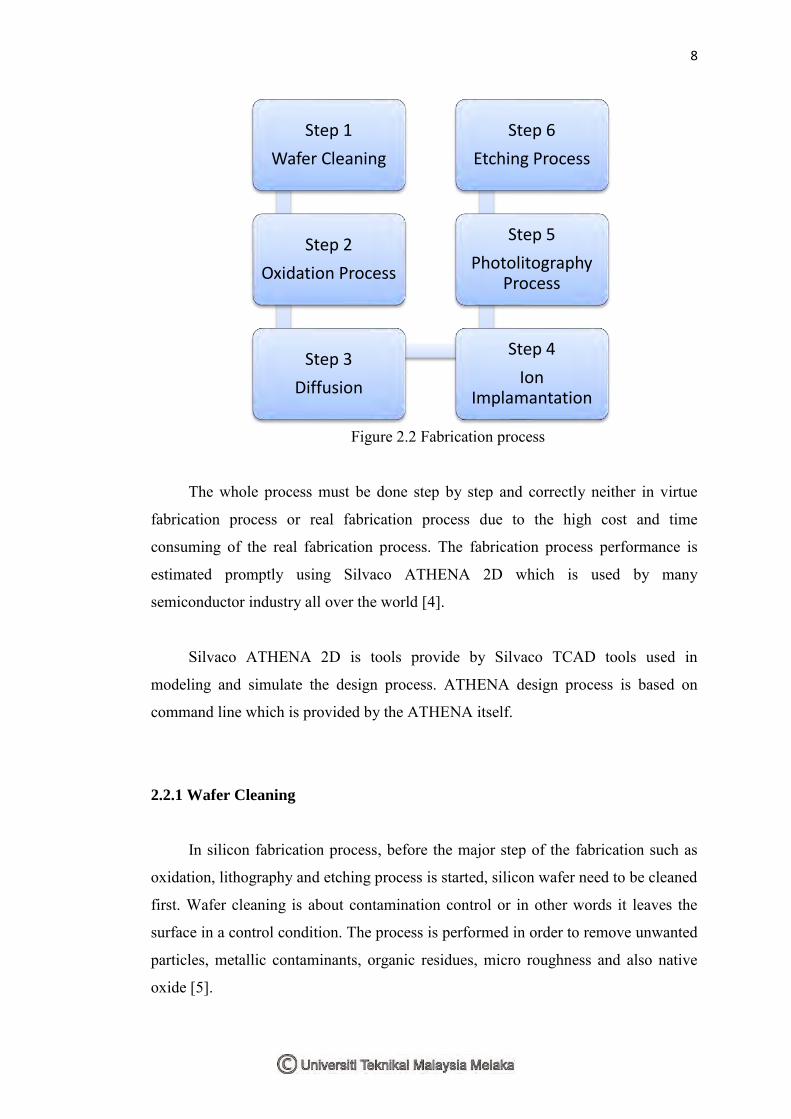
2.2 Silicon Fabrication Process
In silicon fabrication process there are several step need to be done in order to
produce the silicon waveguide as shown in Figure 2.2.
8
Figure 2.2 Fabrication process
The whole process must be done step by step and correctly neither in virtue
fabrication process or real fabrication process due to the high cost and time
consuming of the real fabrication process. The fabrication process performance is
estimated promptly using Silvaco ATHENA 2D which is used by many
semiconductor industry all over the world [4].
Silvaco ATHENA 2D is tools provide by Silvaco TCAD tools used in
modeling and simulate the design process. ATHENA design process is based on
command line which is provided by the ATHENA itself.
2.2.1 Wafer Cleaning
In silicon fabrication process, before the major step of the fabrication such as
oxidation, lithography and etching process is started, silicon wafer need to be cleaned
first. Wafer cleaning is about contamination control or in other words it leaves the
surface in a control condition. The process is performed in order to remove unwanted
particles, metallic contaminants, organic residues, micro roughness and also native
oxide [5].
Step 1
Wafer Cleaning
Step 2
Oxidation Process
Step 3
Diffusion
Step 4
Ion Implamantation
Step 5
Photolitography Process
Step 6
Etching Process
9
2.2.2 Oxidation Process
The first basic processing step is silicon fabrication oxidation process or also
called as oxide growth. Oxidation is the process by which a layer of silicon dioxide
(SIO2) is formed on the surface of the silicon wafer [5]. The oxide growth both on
the silicon surface as indicated in Figure 2.2. Typically, about 56% of the oxide
thickness is above the original surface while about 44% is below the original surface.
The oxide thickness, designated tox, can be grown using either dry or wet techniques,
with the former achieving lower defect densities. Typically, oxide thickness varies
from less than 150Å for gate oxides to more than 10000Å for field oxides. Oxidation
takes place at temperature ranging from 700 -1100°C with the resulting oxide
thickness being proportional to the temperature at which it is grown (for a fixed
amount of time).
Figure 2.2 Silicon dioxide growths at the surface of the silicon wafer
2.2.3 Diffusion
The second basic processing step is diffusion [5]. Diffusion in semiconductor
material is the movement of impurity atoms at the surface of the material into the
bulk of the material. Diffusion takes place at temperatures in the range of 800-1400
°C in the same way as a gas diffuses in air. The concentration profile of the impurity
in the semiconductor is a function of the concentration of the impurity at the surface