29
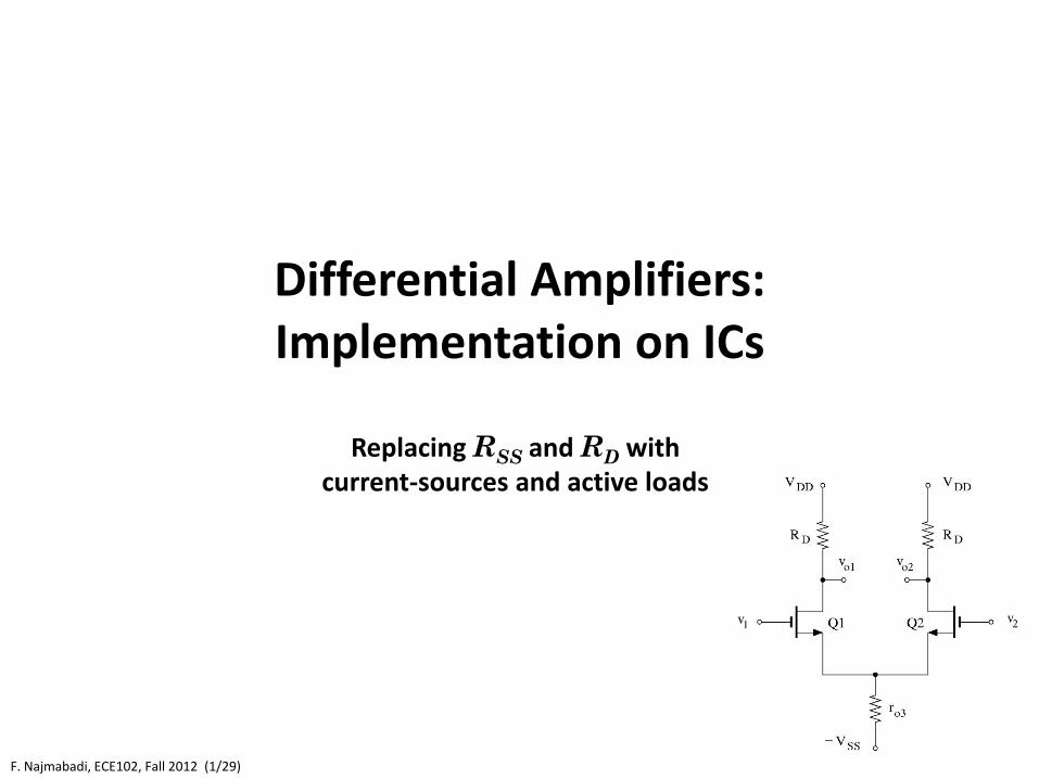
F. Najmabadi, ECE102, Fall 2012 (1/29) Differential Amplifiers: Implementation on ICs Replacing R SS and R D with current-sources and active loads
F. Najmabadi, ECE102, Fall 2012 (1/29)
Differential Amplifiers: Implementation on ICs
Replacing RSS and RD with current-sources and active loads

ID
ID
Resistor Rss provides source degeneration for a stable bias
F. Najmabadi, ECE102, Fall 2012 (2/29)
ID ID
ID ID
2ID
Bias (Common Mode circuit )
In discrete circuits, bias is similar to that of a CS amplifier (source degeneration with a source resistor).
However RSS does not affect the differential gain and , in fact, should be large to improve CMRR (no need for a by-pass capacitor!)
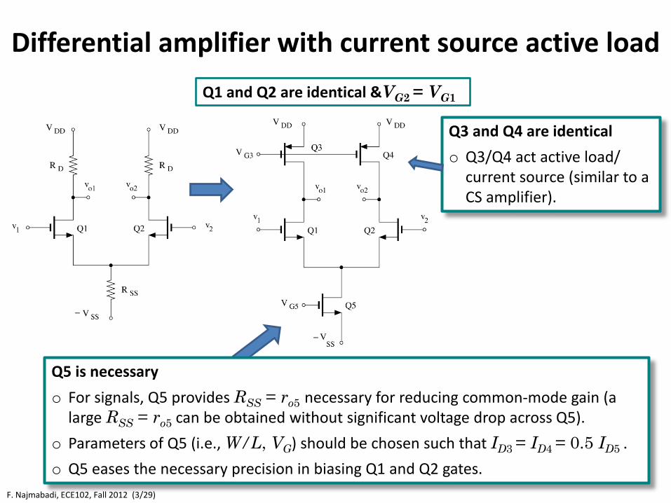
Differential amplifier with current source active load
F. Najmabadi, ECE102, Fall 2012 (3/29)
Q1 and Q2 are identical &VG2 = VG1
Q3 and Q4 are identical
o Q3/Q4 act active load/ current source (similar to a CS amplifier).
Q5 is necessary
o For signals, Q5 provides RSS = ro5 necessary for reducing common-mode gain (a large RSS = ro5 can be obtained without significant voltage drop across Q5).
o Parameters of Q5 (i.e., W/L, VG) should be chosen such that ID3 = ID4 = 0.5 ID5 . o Q5 eases the necessary precision in biasing Q1 and Q2 gates.

Differential amplifier with current source active load – Bias
F. Najmabadi, ECE102, Fall 2012 (4/29)
Q1 and Q2 are identical & VG2 = VG1
Q3 and Q4 are identical
Parameters of Q5 (i.e., W/L, VG) are chosen such that ID3 = ID4 = 0.5 ID5
54321
2121
5.0
DDDDD
OVOVGSGS
IIIIIVVVV
=====⇒=
Ignoring channel-width modulation:* 1. ID1 = ID3 = 0.5 ID5 sets VOV1 and VGS1 2. VS1 = VGS1 −VG1 3. VD5 = VS1 4. VDS5 = VS1 +VSS 5. We need to include channel-width modulation to
find VDS1 and VDS3 6. Precise biasing of Q1 and Q2 are not necessary to
get correct ID1 (it only affects VDS1 and VDS3 )*
* Similar results are obtained if we do not ignore channel-width modulation: VS =VD5 will adjust to get the correct VGS1 and VOV1 (See problem set)
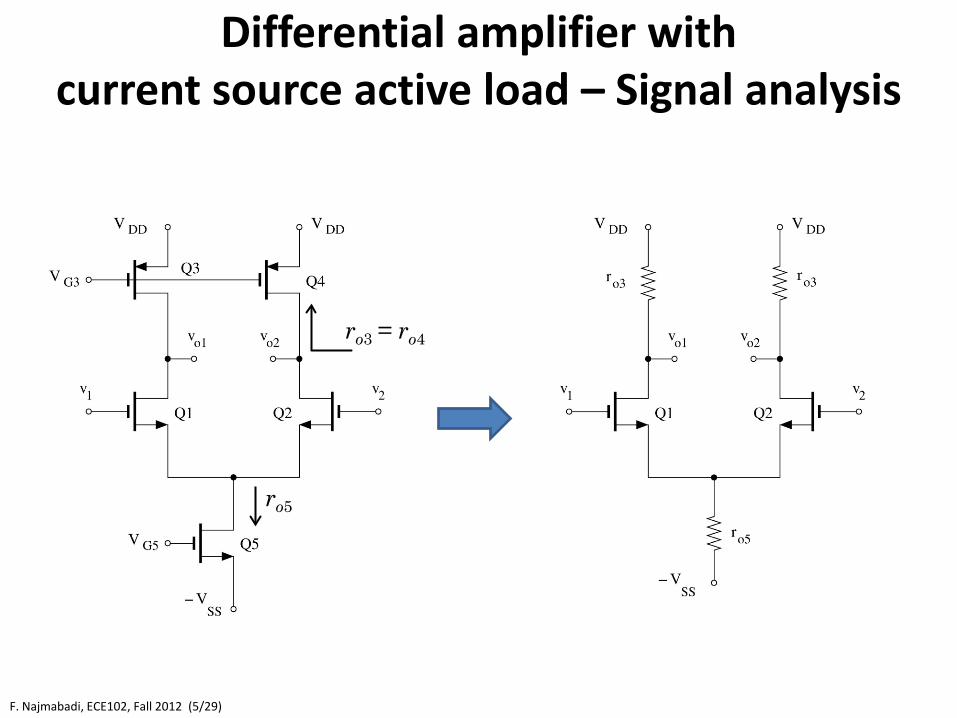
Differential amplifier with current source active load – Signal analysis
F. Najmabadi, ECE102, Fall 2012 (5/29)
ro3 = ro4
ro5

Differential amplifier with current source active load – Signal analysis
F. Najmabadi, ECE102, Fall 2012 (6/29)
Common Mode
dmodo
dmdmdo
vrrgvvvrrgvrrgv
)||(5.0 )||(5.0)5.0( )||(
o3o111,2
o3o11o3o11,1
−=−=
=−−=
coco
ooom
om
c
co
vvrrrg
rgv
v
,2,1
1351
31,1
/21
=++
−=
Differential Mode
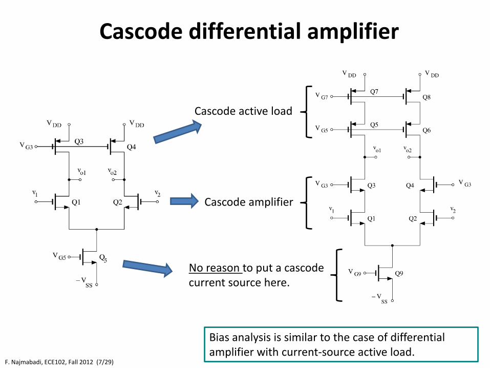
Cascode differential amplifier
F. Najmabadi, ECE102, Fall 2012 (7/29)
Cascode amplifier
Cascode active load
Bias analysis is similar to the case of differential amplifier with current-source active load.
No reason to put a cascode current source here.
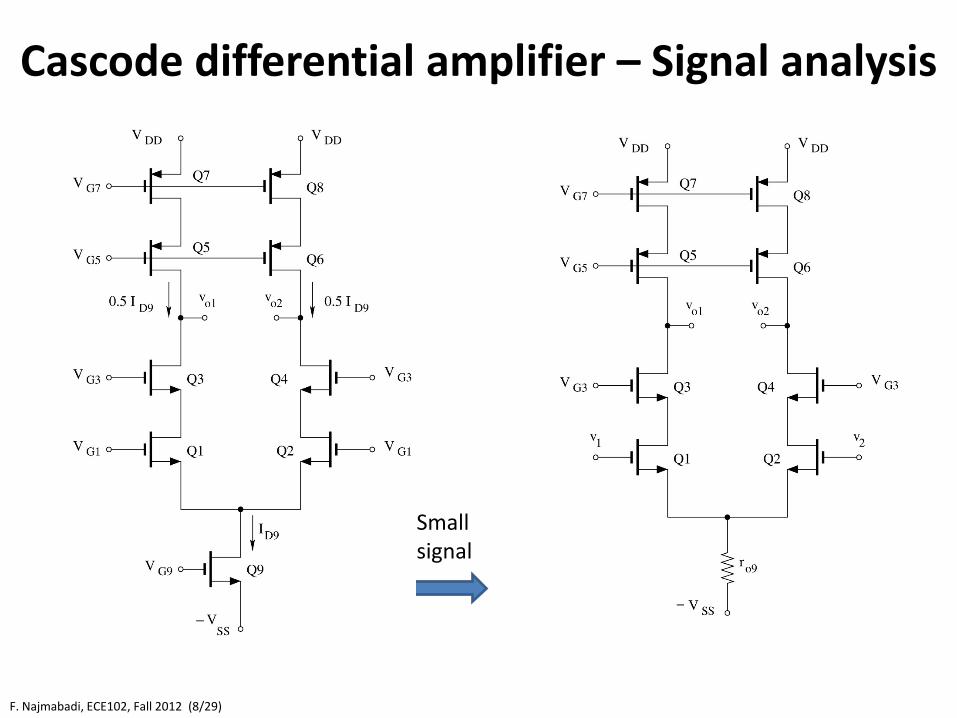
Cascode differential amplifier – Signal analysis
F. Najmabadi, ECE102, Fall 2012 (8/29)
Small signal

Cascode differential amplifier – Signal analysis
F. Najmabadi, ECE102, Fall 2012 (9/29)
Differential Mode
( )dodo
dmmm
doomoom
oooommmdo
vvvrrgrrgg
vrrgrrgrrrrgggv
,1,2
o7o55o1o331
755313
7531531,1
)5.0( ||
)5.0(
−=−−=
−×+
−≈
From Lecture Set 6:
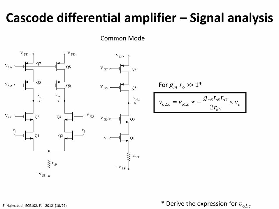
Cascode differential amplifier – Signal analysis
F. Najmabadi, ECE102, Fall 2012 (10/29)
Common Mode
2
9
755,1,2 c
o
oomcoco v
rrrgvv ×−≈=
For gm ro >> 1*
* Derive the expression for vo1,c
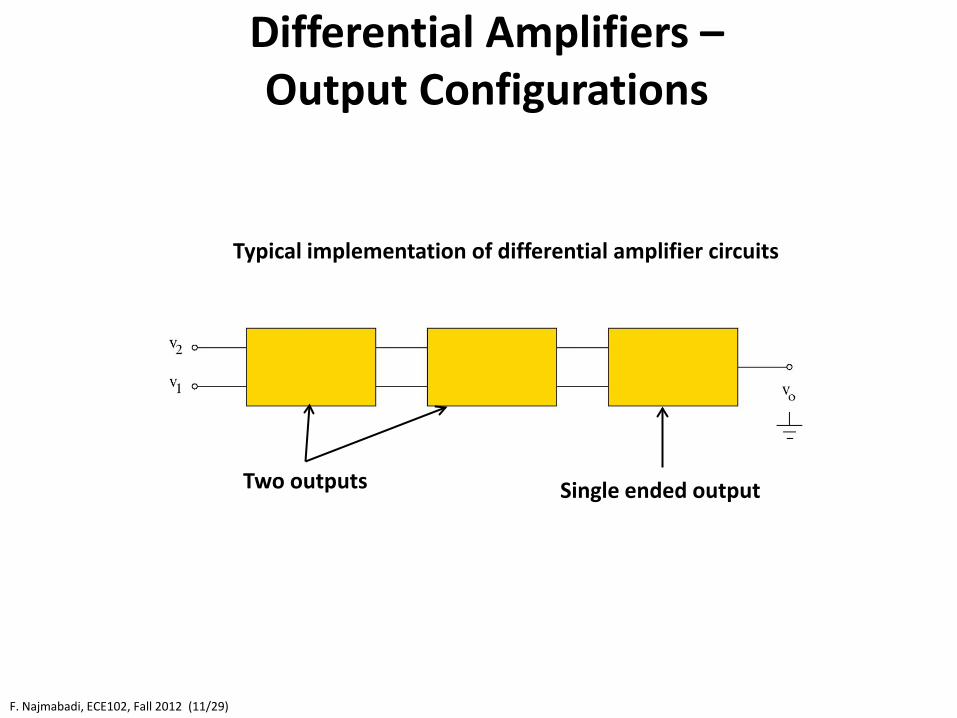
Differential Amplifiers – Output Configurations
F. Najmabadi, ECE102, Fall 2012 (11/29)
Typical implementation of differential amplifier circuits
Two outputs Single ended output
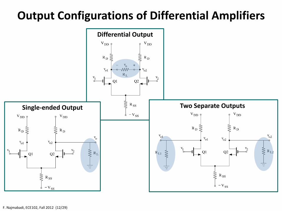
Output Configurations of Differential Amplifiers
F. Najmabadi, ECE102, Fall 2012 (12/29)
Differential Output
Single-ended Output
Two Separate Outputs
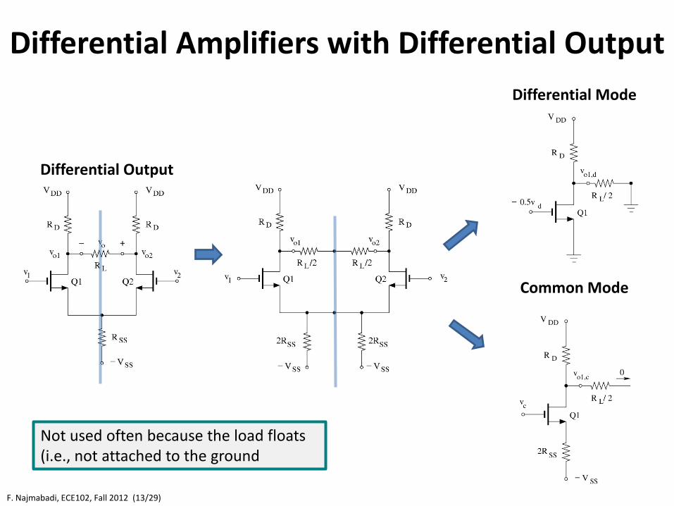
Differential Amplifiers with Differential Output
F. Najmabadi, ECE102, Fall 2012 (13/29)
Differential Output
Differential Mode
Common Mode
Not used often because the load floats (i.e., not attached to the ground
Differential Amplifiers with Differential Output
F. Najmabadi, ECE102, Fall 2012 (14/29)
Differential Output
Differential Mode
Common Mode
/2)||||(
/2)||||(2
)5.0/2)(||||(
,1,1,2
,1,2
,1
LDomd
odd
dLDomdododood
dodo
dLDomdo
RRrgvvA
vRRrgvvvvvv
vRRrgv
−==
−=−=−=
−=
−−=
0
0
/21
,1,2
,1,2
,1
==
=−=
=++
−=
c
occ
cocooc
coco
oDSSm
Dm
c
co
vvA
vvvvv
rRRgRg
vv
∞==||||CMRR
c
d
AA
ddcco vAvAv ⋅+⋅=
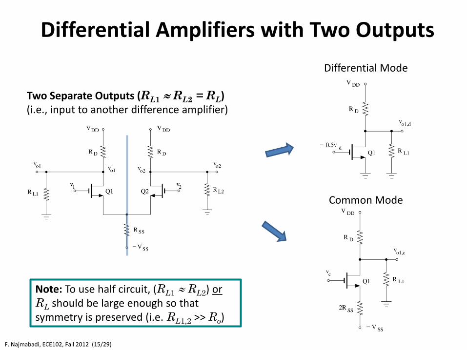
Differential Amplifiers with Two Outputs
F. Najmabadi, ECE102, Fall 2012 (15/29)
Differential Mode
Common Mode
Two Separate Outputs (RL1 ≈ RL2 = RL) (i.e., input to another difference amplifier)
Note: To use half circuit, (RL1 ≈ RL2) or RL should be large enough so that symmetry is preserved (i.e. RL1,2 >> Ro)
Differential Amplifiers with Two Outputs
F. Najmabadi, ECE102, Fall 2012 (16/29)
oLDSSm
LDm
c
co
oLDSSm
LDm
c
co
rRRRgRRg
vv
rRRRgRRg
vv
/)||(21)||(
/)||(21)||(
2
2,2
1
1,1
++−=
++−=
Differential Mode
Common Mode
)||||(5.0
)||||(5.0
2,2
1,1
LDomd
do
LDomd
do
RRrgv
v
RRrgv
v
−=+
−=−
Note: Each output has its own differential- and common-mode gains: ddcco
c
coc
d
dod
vAvAvv
vA
vv
A
⋅+⋅=
==
111
,11
,11 ,
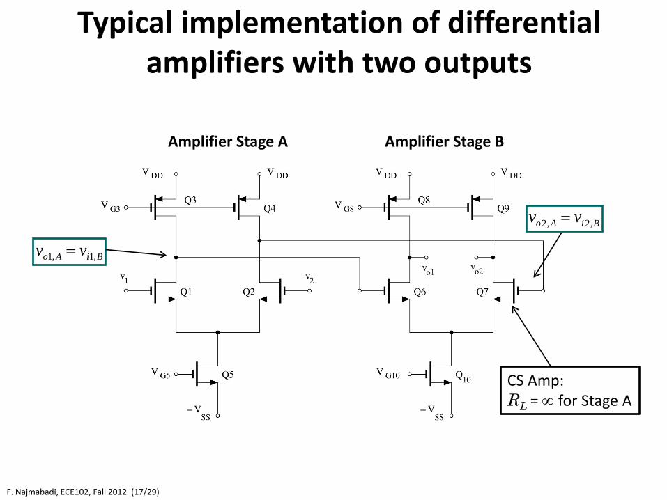
Typical implementation of differential amplifiers with two outputs
F. Najmabadi, ECE102, Fall 2012 (17/29)
BiAo vv ,1,1 =
Amplifier Stage A Amplifier Stage B
BiAo vv ,2,2 =
CS Amp: RL = ∞ for Stage A
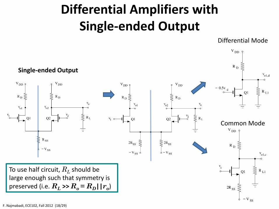
Differential Amplifiers with Single-ended Output
F. Najmabadi, ECE102, Fall 2012 (18/29)
Single-ended Output
Differential Mode
Common Mode
To use half circuit, RL should be large enough such that symmetry is preserved (i.e. RL >> Ro = RD||ro)
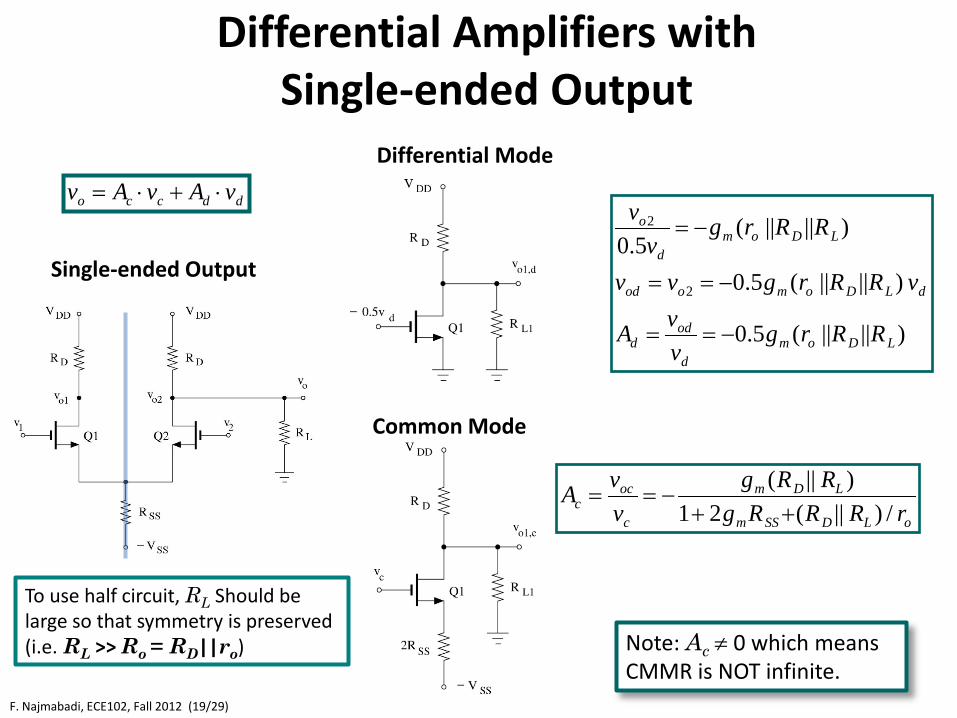
Differential Amplifiers with Single-ended Output
F. Najmabadi, ECE102, Fall 2012 (19/29)
Single-ended Output
Differential Mode
Common Mode
)||||(5.0
)||||(5.0
)||||(5.0
2
2
LDomd
odd
dLDomood
LDomd
o
RRrgvvA
vRRrgvv
RRrgv
v
−==
−==
−=
oLDSSm
LDm
c
occ rRRRg
RRgvvA
/)||(21)||(
++−==
ddcco vAvAv ⋅+⋅=
To use half circuit, RL Should be large so that symmetry is preserved (i.e. RL >> Ro = RD||ro) Note: Ac ≠ 0 which means
CMMR is NOT infinite.
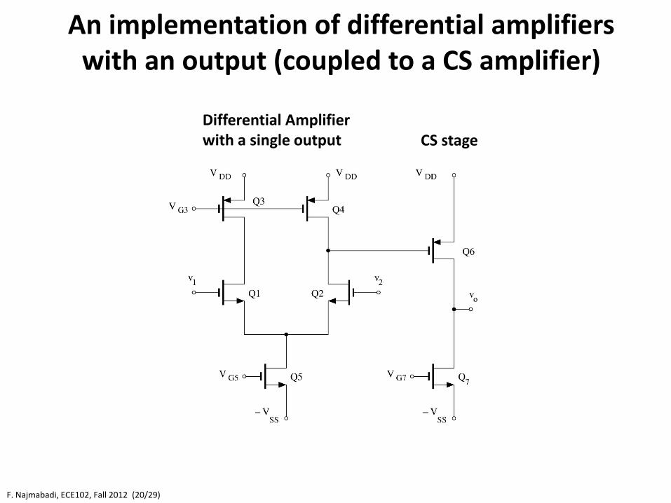
An implementation of differential amplifiers with an output (coupled to a CS amplifier)
F. Najmabadi, ECE102, Fall 2012 (20/29)
CS stage Differential Amplifier with a single output
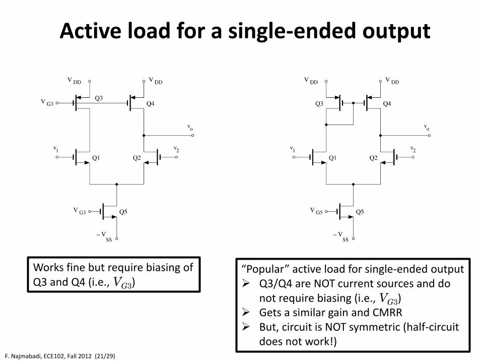
Active load for a single-ended output
F. Najmabadi, ECE102, Fall 2012 (21/29)
Works fine but require biasing of Q3 and Q4 (i.e., VG3)
“Popular” active load for single-ended output Q3/Q4 are NOT current sources and do
not require biasing (i.e., VG3) Gets a similar gain and CMRR But, circuit is NOT symmetric (half-circuit
does not work!)

Active load for a single-ended output: Small signal equivalent
F. Najmabadi, ECE102, Fall 2012 (22/29)
Small Signal
Diode-connected transistor
Note ro4 = ro3 and gm4 = gm3

Small-signal analysis of single-ended output
F. Najmabadi, ECE102, Fall 2012 (23/29)
Note ro4 = ro3 and gm4 = gm3 ro2 = ro1 and gm2 = gm1
Small Signal
Circuit is NOT symmetric CANNOT use “half-circuit”
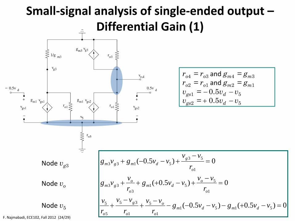
Small-signal analysis of single-ended output – Differential Gain (1)
F. Najmabadi, ECE102, Fall 2012 (24/29)
ro4 = ro3 and gm4 = gm3 ro2 = ro1 and gm2 = gm1 vgs1 = − 0.5vd − v5 vgs2 = + 0.5vd − v5
0)5.0()5.0(
0)5.0(
0)5.0(
51511
5
1
35
5
5
1
551
333
1
535133
=−+−−−−−
+−
+
=−
+−+++
=−
+−−+
vvgvvgr
vvr
vvrv
rvvvvg
rvvg
rvv
vvgvg
dmdmo
o
o
g
o
o
odm
o
ogm
o
gdmgmNode vg3
Node vo
Node v5

Small-signal analysis of single-ended output – Differential Gain (2)
F. Najmabadi, ECE102, Fall 2012 (25/29)
( )
011221
5.0111
5.011
15115
13
1131
1533
11
151
33
=
−+
++++
−
−=
++
−−+
+=
−−+
+
oo
oom
og
dmoo
oo
mmg
dmo
mo
mg
rv
rrgv
rv
vgrr
vr
gvgv
vgr
gvr
gv
Dropping 1/ro terms compared with gm
Rearranging terms:
( ) ( )
( ) ( )
( ) 0121
5.011
5.0
115
13
113
1533
11533
=
−+++
−
−=
++−+
+=−+
oom
og
dmoo
ommg
dmmmg
rvgv
rv
vgrr
vgvgv
vggvgvDropping v5 /ro5 term implies that very little current flows into ro5 (can remove ro5 from the circuit as done in the textbook)
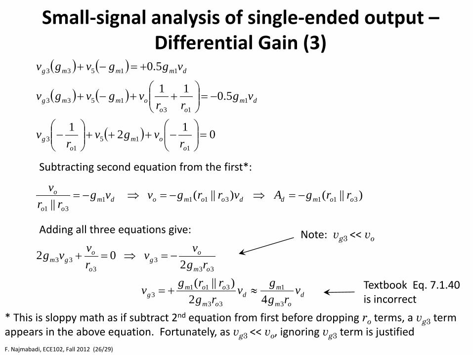
Small-signal analysis of single-ended output – Differential Gain (3)
F. Najmabadi, ECE102, Fall 2012 (26/29)
( ) ( )
( ) ( )
( ) 0121
5.011
5.0
115
13
113
1533
11533
=
−+++
−
−=
++−+
+=−+
oom
og
dmoo
ommg
dmmmg
rvgv
rv
vgrr
vgvgv
vggvgv
Subtracting second equation from the first*:
)||( )||( || 3113111
31oomddoomodm
oo
o rrgAvrrgvvgrr
v−=⇒−=⇒−=
* This is sloppy math as if subtract 2nd equation from first before dropping ro terms, a vg3 term appears in the above equation. Fortunately, as vg3 << vo, ignoring vg3 term is justified
Adding all three equations give:
dom
md
om
oomg
om
og
o
ogm
vrg
gvrg
rrgv
rgvv
rvvg
3
1
33
3113
333
333
42)||(
2 0 2
≈+=
−=⇒=+
Note: vg3 << vo
Textbook Eq. 7.1.40 is incorrect
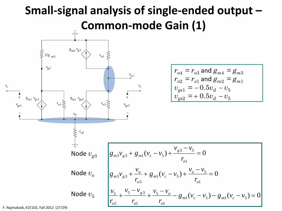
Small-signal analysis of single-ended output – Common-mode Gain (1)
F. Najmabadi, ECE102, Fall 2012 (27/29)
ro4 = ro3 and gm4 = gm3 ro2 = ro1 and gm2 = gm1 vgs1 = − 0.5vd − v5 vgs2 = + 0.5vd − v5
0)()(
0)(
0)(
51511
5
1
35
5
5
1
551
333
1
535133
=−−−−−
+−
+
=−
+−++
=−
+−+
vvgvvgr
vvr
vvrv
rvvvvg
rvvg
rvv
vvgvg
cmcmo
o
o
g
o
o
ocm
o
ogm
o
gcmgmNode vg3
Node vo
Node v5
Small-signal analysis of single-ended output – Common-mode Gain (2)
F. Najmabadi, ECE102, Fall 2012 (28/29)
0)()(
0)(
0)(
51511
5
1
35
5
5
1
551
333
1
535133
=−−−−−
+−
+
=−
+−++
=−
+−+
vvgvvgr
vvr
vvrv
rvvvvg
rvvg
rvv
vvgvg
cmcmo
o
o
g
o
o
ocm
o
ogm
o
gcmgm
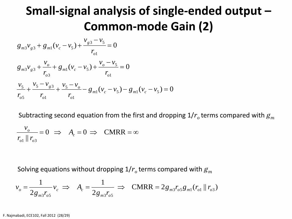
Subtracting second equation from the first and dropping 1/ro terms compared with gm
∞=⇒=⇒= CMRR 0 0|| 31
coo
o Arr
v
)||(2CMRR 2
1 2
131153
5353oomom
omcc
omo rrgrg
rgAv
rgv =⇒=⇒=
Solving equations without dropping 1/ro terms compared with gm

Small-signal analysis of single-ended output –Output Resistance
F. Najmabadi, ECE102, Fall 2012 (29/29)
0)()(
)(
0)(
51511
5
1
35
5
5
1
551
333
1
535133
=−−−−−
+−
+
=−
+−++
=−
+−+
vgvgr
vvr
vvrv
ir
vvvgrvvg
rvv
vgvg
mmo
x
o
g
o
xo
xm
o
xgm
o
gmgmNode vg3
Node vx
Node v5
Subtracting second equation from the first and dropping 1/ro terms compared with gm
31
31
||
||
oox
xo
xoo
x
rrivR
irr
v
==
=
Attach a source vx to the output and calculate ix)
![Cascode Switching Modeling and Improvement in Flyback ...Cascode GaN FET [10], during inductive hard switching. Figure 2 Cascode Switching Configured Flyback converter II. MODELING](https://static.documents.pub/doc/80x56/5e541119f61a9f6e2b2e813c/cascode-switching-modeling-and-improvement-in-flyback-cascode-gan-fet-10.jpg)


