60
July 10, 2002 09:55 vra23151_ch10 Sheet number 1 Page number 605 black 605 chapter 10 Digital System Design a b c d e f g h 1 2 3 4 5 6 7 8 10. Bd3–g6+, Ke8–d8

July 10, 2002 09:55 vra23151_ch10 Sheet number 1 Page number 605 black
605
c h a p t e r
10Digital System Design
a b c d e f g h
1
2
3
4
5
6
7
8
10. Bd3–g6+, Ke8–d8

July 10, 2002 09:55 vra23151_ch10 Sheet number 2 Page number 606 black
606 C H A P T E R 10 • Digital System Design
In the previous chapters we showed how to design many types of simple circuits, such as multiplexers,decoders, flip-flops, registers, and counters, which can be used as building blocks. In this chapter we provideexamples of more complex circuits that can be constructed using the building blocks as subcircuits. Suchlarger circuits form a digital system. For practical reasons our examples of digital systems will not be large,but the design techniques presented are applicable to systems of any size. After presenting several examples,we will discuss some practical issues, such as how to ensure reliable clocking of flip-flops in individual andmultiple chips, how to deal with input signals that are not synchronized to the clock signal, and the like.
A digital system consists of two main parts, called the datapath circuit and the control circuit. Thedatapath circuit is used to store and manipulate data and to transfer data from one part of the system toanother. Datapath circuits comprise building blocks such as registers, shift registers, counters, multiplexers,decoders, adders, and so on. The control circuit controls the operation of the datapath circuit. In Chapter 8we referred to the control circuits as finite state machines.
10.1 Building Block Circuits
We will give several examples of digital systems and show how to design their datapathand control circuits. The examples use a number of the building block circuits that werepresented in earlier chapters. Some building blocks used in this chapter are described below.
10.1.1 Flip-Flops and Registers with Enable Inputs
In many applications that use D flip-flops, it is useful to be able to prevent the data storedin the flip-flop from changing when an active clock edge occurs. We showed in Figure 7.61how this capability can be provided by adding a multiplexer to the flip-flop. Figure 10.1depicts the circuit. When E = 0, the flip-flop output cannot change, because the multiplexerconnects Q to D. But if E = 1, then the multiplexer connects the R input to D. Instead ofusing the multiplexer shown in the figure, another way to implement the enable feature is touse a two-input AND gate that drives the flip-flop’s clock input. One input to the AND gateis the clock signal, and the other input is E. Then setting E = 0 prevents the clock signalfrom reaching the flip-flop’s clock input. This method seems simpler than the multiplexerapproach, but we will show in section 10.3 that it can cause problems in practical operation.
D Q
Q
QR
Clock
E
0
1
Figure 10.1 A flip-flop with an enable input.

July 10, 2002 09:55 vra23151_ch10 Sheet number 3 Page number 607 black
10.1 Building Block Circuits 607
We will prefer the multiplexer-based approach over gating the clock with an AND gate inthis chapter.
Verilog code for a D flip-flop with an asynchronous reset input and an enable input isgiven in Figure 10.2. We can extend the enable capability to registers with n bits by usingn 2-to-1 multiplexers controlled by E. The multiplexer for each flip-flop, i, selects eitherthe external data bit, Ri, or the flip-flop’s output, Qi. Verilog code for an n-bit register withan asynchronous reset input and an enable input is given in Figure 10.3.
10.1.2 Shift Registers with Enable Inputs
It is useful to be able to inhibit the shifting operation in a shift register by using an en-able input, E. We showed in Figure 7.19 that shift registers can be constructed with aparallel-load capability, which is implemented using a multiplexer. Figure 10.4 shows how
module rege (R, Clock, Resetn, E, Q);input R, Clock, Resetn, E;output Q;reg Q;
always @(posedge Clock or negedge Resetn)if (Resetn == 0)
Q <= 0;else if (E)
Q <= R;
endmodule
Figure 10.2 Code for a D flip-flop with enable.
module regne (R, Clock, Resetn, E, Q);parameter n = 8;input [n 1:0] R;input Clock, Resetn, E;output [n 1:0] Q;reg [n 1:0] Q;
always @(posedge Clock or negedge Resetn)if (Resetn == 0)
Q <= 0;else if (E)
Q <= R;
endmodule
Figure 10.3 An n-bit register with an enable input.

July 10, 2002 09:55 vra23151_ch10 Sheet number 4 Page number 608 black
608
DQ Q
Q0
R0
Clo
ck
L 0 1w
E 0 1D
Q Q
Q1
R1
0 1
0 1D
Q Q
Qn-
1
Rn-
1
0 1
0 1
Figure
10.4
Ashiftregisterwithparallel-loadandenablecontrolinputs.

July 10, 2002 09:55 vra23151_ch10 Sheet number 5 Page number 609 black
10.1 Building Block Circuits 609
the enable feature can be added by using an additional multiplexer. If the parallel-loadcontrol input, L, is 1, the flip-flops are loaded in parallel. But if L = 0, the additionalmultiplexer selects new data to be loaded into the flip-flops only if the enable E is 1.
Verilog code that represents the circuit in Figure 10.4 is given in Figure 10.5. WhenL = 1, the register is loaded in parallel from the R input. When L = 0 and E = 1, the datain the shift register is shifted in a right-to-left direction.
10.1.3 Static RandomAccess Memory (SRAM)
We have introduced several types of circuits that can be used to store data. Assume thatwe need to store a large number, m, of data items, each of which consists of n bits. Onepossibility is to use an n-bit register for each data item. We would need to design circuit-ry to control access to each register, both for loading (writing) data into it and for readingdata out.
When m is large, it is awkward to use individual registers to store the data. A betterapproach is to make use of a static random access memory (SRAM) block. An SRAM blockis a two-dimensional array of SRAM cells, where each cell can store one bit of information.
module shiftlne (R, L, E, w, Clock, Q);parameter n = 4;input [n 1:0] R;input L, E, w, Clock;output [n 1:0] Q;reg [n 1:0] Q;integer k;
always @(posedge Clock)begin
if (L)Q <= R;
else if (E)begin
Q[0] <= w;for (k = 1; k < n; k = k+1)
Q[k] <= Q[k 1];end
end
endmodule
Figure 10.5 A right-to-left shift register with an enable input.
July 10, 2002 09:55 vra23151_ch10 Sheet number 6 Page number 610 black
610 C H A P T E R 10 • Digital System Design
If we need to store m items with n bits each, we can use an array of m × n SRAM cells.The dimensions of the SRAM array are called its aspect ratio.
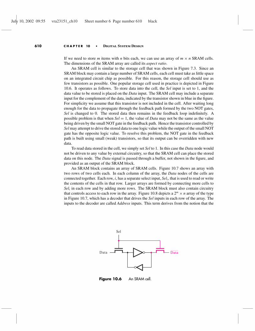
An SRAM cell is similar to the storage cell that was shown in Figure 7.3. Since anSRAM block may contain a large number of SRAM cells, each cell must take as little spaceon an integrated circuit chip as possible. For this reason, the storage cell should use asfew transistors as possible. One popular storage cell used in practice is depicted in Figure10.6. It operates as follows. To store data into the cell, the Sel input is set to 1, and thedata value to be stored is placed on the Data input. The SRAM cell may include a separateinput for the complement of the data, indicated by the transistor shown in blue in the figure.For simplicity we assume that this transistor is not included in the cell. After waiting longenough for the data to propagate through the feedback path formed by the two NOT gates,Sel is changed to 0. The stored data then remains in the feedback loop indefinitely. Apossible problem is that when Sel = 1, the value of Data may not be the same as the valuebeing driven by the small NOT gate in the feedback path. Hence the transistor controlled bySel may attempt to drive the stored data to one logic value while the output of the small NOTgate has the opposite logic value. To resolve this problem, the NOT gate in the feedbackpath is built using small (weak) transistors, so that its output can be overridden with newdata.
To read data stored in the cell, we simply set Sel to 1. In this case the Data node wouldnot be driven to any value by external circuitry, so that the SRAM cell can place the storeddata on this node. The Data signal is passed through a buffer, not shown in the figure, andprovided as an output of the SRAM block.
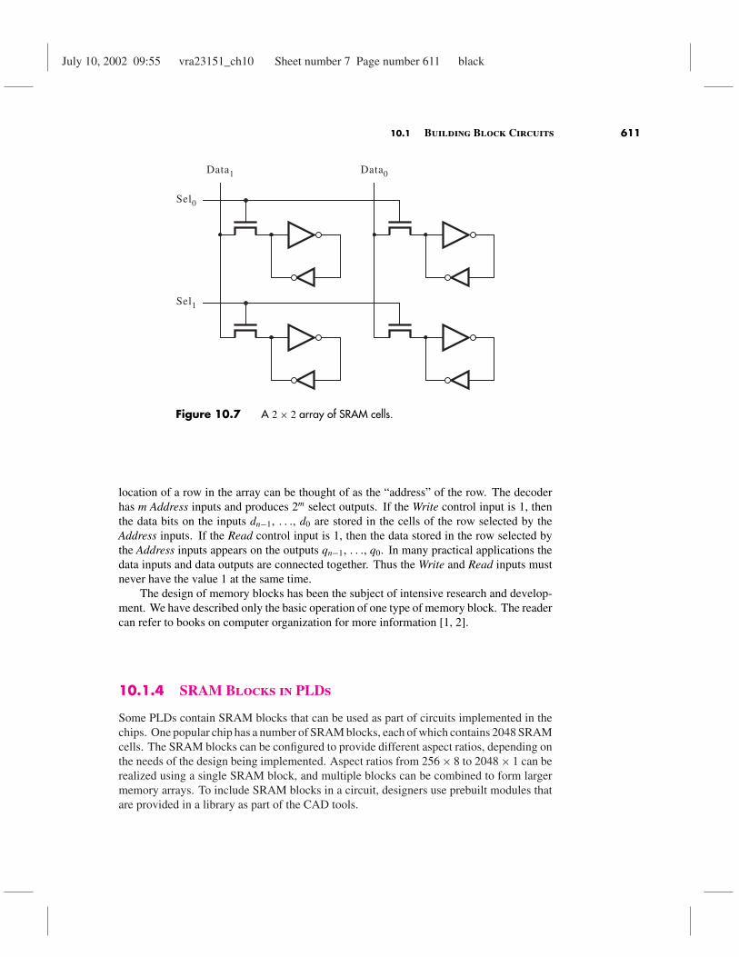
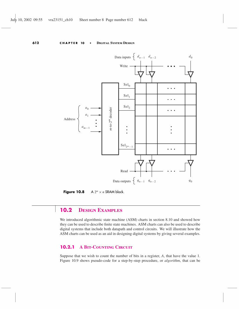
An SRAM block contains an array of SRAM cells. Figure 10.7 shows an array withtwo rows of two cells each. In each column of the array, the Data nodes of the cells areconnected together. Each row, i, has a separate select input, Seli, that is used to read or writethe contents of the cells in that row. Larger arrays are formed by connecting more cells toSeli in each row and by adding more rows. The SRAM block must also contain circuitrythat controls access to each row in the array. Figure 10.8 depicts a 2m × n array of the typein Figure 10.7, which has a decoder that drives the Sel inputs in each row of the array. Theinputs to the decoder are called Address inputs. This term derives from the notion that the
Sel
DataData
Figure 10.6 An SRAM cell.
July 10, 2002 09:55 vra23151_ch10 Sheet number 7 Page number 611 black
10.1 Building Block Circuits 611
Sel1
Sel0
Data0Data1
Figure 10.7 A 2× 2 array of SRAM cells.
location of a row in the array can be thought of as the “address” of the row. The decoderhas m Address inputs and produces 2m select outputs. If the Write control input is 1, thenthe data bits on the inputs dn−1, . . ., d0 are stored in the cells of the row selected by theAddress inputs. If the Read control input is 1, then the data stored in the row selected bythe Address inputs appears on the outputs qn−1, . . ., q0. In many practical applications thedata inputs and data outputs are connected together. Thus the Write and Read inputs mustnever have the value 1 at the same time.
The design of memory blocks has been the subject of intensive research and develop-ment. We have described only the basic operation of one type of memory block. The readercan refer to books on computer organization for more information [1, 2].
10.1.4 SRAM Blocks in PLDs
Some PLDs contain SRAM blocks that can be used as part of circuits implemented in thechips. One popular chip has a number of SRAM blocks, each of which contains 2048 SRAMcells. The SRAM blocks can be configured to provide different aspect ratios, depending onthe needs of the design being implemented. Aspect ratios from 256× 8 to 2048× 1 can berealized using a single SRAM block, and multiple blocks can be combined to form largermemory arrays. To include SRAM blocks in a circuit, designers use prebuilt modules thatare provided in a library as part of the CAD tools.
July 10, 2002 09:55 vra23151_ch10 Sheet number 8 Page number 612 black
612 C H A P T E R 10 • Digital System Design
Sel2
Sel1
Sel0
Sel2m 1–
Read
Write
d0dn 1– dn 2–
q0qn 1– qn 2–
m-t
o-2m
dec
oder
Address
a0
a1
am 1–
Data outputs
Data inputs
Figure 10.8 A 2m × n SRAM block.
10.2 Design Examples
We introduced algorithmic state machine (ASM) charts in section 8.10 and showed howthey can be used to describe finite state machines. ASM charts can also be used to describedigital systems that include both datapath and control circuits. We will illustrate how theASM charts can be used as an aid in designing digital systems by giving several examples.
10.2.1 A Bit-Counting Circuit
Suppose that we wish to count the number of bits in a register, A, that have the value 1.Figure 10.9 shows pseudo-code for a step-by-step procedure, or algorithm, that can be

July 10, 2002 09:55 vra23151_ch10 Sheet number 9 Page number 613 black
10.2 Design Examples 613
B = 0 ;while A � 0 do
if a0 = 1 thenB = B + 1 ;
end if ;Right-shift A ;
end while ;
Figure 10.9 Pseudo-code for the bit counter.
used to perform the required task. It assumes that A is stored in a register that can shift itscontents in the left-to-right direction. The answer produced by the algorithm is stored inthe variable named B. The algorithm terminates when A does not contain any more 1s, thatis when A = 0. In each iteration of the while loop, if the least-significant bit (LSB) of A is1, then B is incremented by 1; otherwise, B is not changed. A is shifted one bit to the rightat the end of each loop iteration.
Figure 10.10 gives an ASM chart that represents the algorithm in Figure 10.9. The statebox for the starting state, S1, specifies that B is initialized to 0. We assume that an inputsignal, s, exists, which is used to indicate when the data to be processed has been loadedinto A, so that the machine can start. The decision box labeled s stipulates that the machineremains in state S1 as long as s = 0. The conditional output box with Load A written insideit indicates that A is loaded from external data inputs if s = 0 in state S1.
When s becomes 1, the machine changes to state S2. The decision box below the statebox for S2 checks whether A = 0. If so, the bit-counting operation is complete; hence themachine should change to state S3. If not, the FSM remains in state S2. The decision boxat the bottom of the chart checks the value of a0. If a0 = 1, B is incremented, which isindicated in the chart as B ← B + 1. If a0 = 0, then B is not changed. In state S3, Bcontains the result, which is the number of bits in A that were 1. An output signal, Done, isset to 1 to indicate that the algorithm is finished; the FSM stays in S3 until s goes back to 0.
10.2.2 ASM Chart Implied Timing Information
In section 8.10 we said that ASM charts are similar to traditional flowcharts, except that theASM chart implies timing information. We can use the bit-counting example to illustratethis concept. Consider the ASM block for state S2, which is shaded in blue in Figure 10.10.In a traditional flowchart, when state S2 is entered, the value of A would first be shifted tothe right. Then we would examine the value of A and if A’s LSB is 1, we would immediatelyadd 1 to B. But, since the ASM chart represents a sequential circuit, changes in A and B,which represent the outputs of flip-flops, take place after the active clock edge. The sameclock signal that controls changes in the state of the machine also controls changes in Aand B. Hence in state S2, the decision box that tests whether A = 0, as well as the boxthat checks the value of a0, check the bits in A before they are shifted. If A = 0, then theFSM will change to state S3 on the next clock edge (this clock edge also shifts A, whichhas no effect because A is already 0 in this case.) On the other hand, if A �= 0, then the

July 10, 2002 09:55 vra23151_ch10 Sheet number 10 Page number 614 black
614 C H A P T E R 10 • Digital System Design
Shift right A Done
B B 1+← A 0= ?
B 0←
s
Load A
a0
Reset
S3
0
1
0
1
0
1s
S1
S2
1
0
Figure 10.10 ASM chart for the pseudo-code in Figure 10.9.
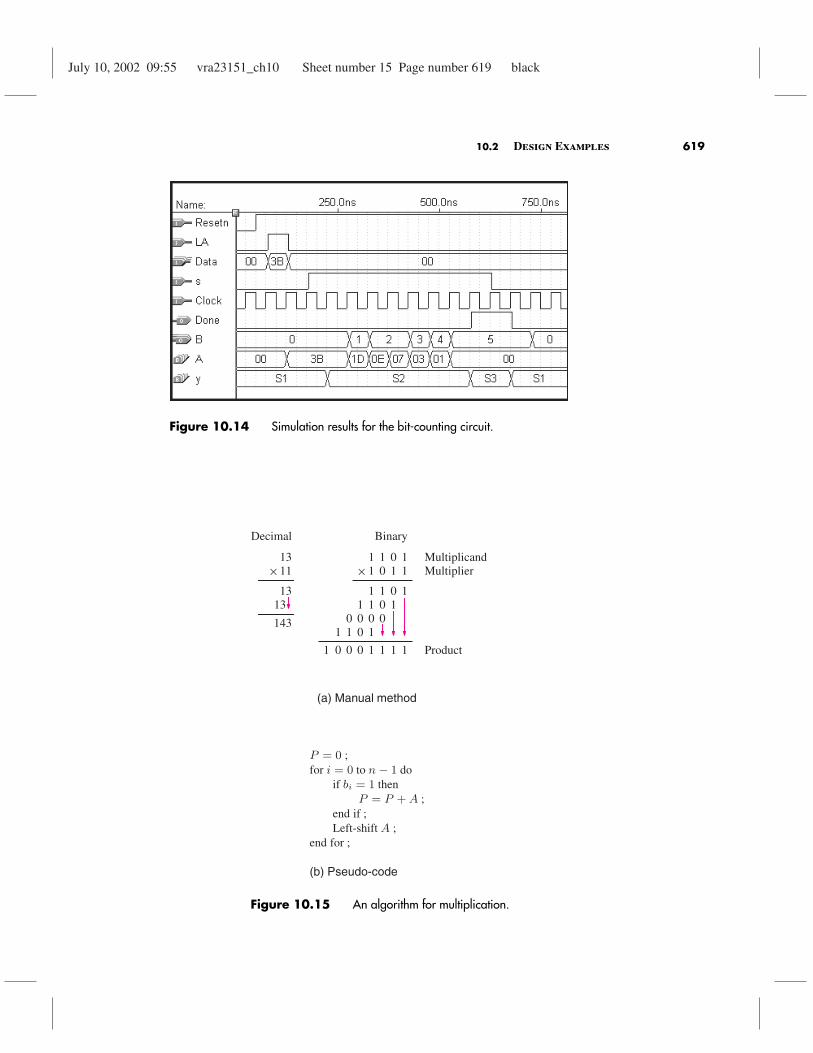
FSM does not change to S3, but remains in S2. At the same time, A is still shifted, and Bis incremented if a0 has the value 1. These timing issues are illustrated in Figure 10.14,which represents a simulation result for a circuit that implements the ASM chart. We showhow the circuit is designed in the following discussion.
Datapath CircuitBy examining theASM chart for the bit-counting circuit, we can infer the type of circuit
elements needed to implement its datapath. We need a shift register that shifts left-to-rightto implement A. It must have the parallel-load capability because of the conditional outputbox in state S1 that loads data into the register. An enable input is also required becauseshifting should occur only in state S2. A counter is needed for B, and it needs a parallel-loadcapability to initialize the count to 0 in state S1. It is not wise to rely on the counter’s resetinput to clear B to 0 in state S1. In practice, the reset signal is used in a digital system foronly two purposes: to initialize the circuit when power is first applied, or to recover from

July 10, 2002 09:55 vra23151_ch10 Sheet number 11 Page number 615 black
10.2 Design Examples 615
L
E Counter
w
L
EShift
LB
EBLA
EA
0
Clock
0
Bz a0
Data
n
A
n
(log2 n) + 1
(log2 n) + 1
Figure 10.11 Datapath for the ASM chart in Figure 10.10.
an error. The machine changes from state S3 to S1 as a result of s = 0; hence we shouldnot assume that the reset signal is used to clear the counter.
The datapath circuit is depicted in Figure 10.11. The serial input to the shift register, w,is connected to 0, because it is not needed. The load and enable inputs on the shift registerare driven by the signals LA and EA. The parallel input to the shift register is named Data,and its parallel output is A. An n-input NOR gate is used to test whether A = 0. The outputof this gate, z, is 1 when A = 0. Note that the figure indicates the n-input NOR gate byshowing a single input connection to the gate, with the label n attached to it. The counterhas log2(n) bits, with parallel inputs connected to 0 and parallel outputs named B. It alsohas a parallel load input LB and enable input EB control signals.
Control CircuitFor convenience we can draw a second ASM chart that represents only the FSM needed
for the control circuit, as shown in Figure 10.12. The FSM has the inputs s, a0, and z andgenerates the outputs EA, LB, EB, and Done. In state S1, LB is asserted, so that 0 is loadedin parallel into the counter. Note that for the control signals, like LB, instead of writing LB= 1, we simply write LB to indicate that the signal is asserted. We assume that externalcircuitry drives LA to 1 when valid data is present at the parallel inputs of the shift register,so that the shift register contents are initialized before s changes to 1. In state S2, EA isasserted to cause a shift operation, and the count enable for B is asserted only if a0 = 1.

July 10, 2002 09:55 vra23151_ch10 Sheet number 12 Page number 616 black
616 C H A P T E R 10 • Digital System Design
EA
EB z
LB
s
a0
Reset
S3
0
1
0
1
0
1s
S2
S1
0
1
Done
Figure 10.12 ASM chart for the bit counter datapath circuit.
Verilog CodeThe bit-counting circuit can be described in Verilog code as shown in Figure 10.13.
We have chosen to define A as an eight-bit vector and B as a 4-bit vector signal. The ASMchart in Figure 10.12 can be directly translated into code that describes the required controlcircuit. The signal y is used to represent the present state of the FSM, and Y represents thenext state. The FSM is described with three always blocks: the block labeled State_tablespecifies the state transitions, the block labeled State_ flipflops represents the state flip-flops,and the block labeled FSM_outputs specifies the generated outputs in each state. A defaultvalue is specified at the beginning of the FSM_outputs block for each output signal, andthen individual output values are specified in the case statement.
The fourth always block defines the up-counter that implements B. The shift registerfor A is instantiated at the end of the code, and the z signal is defined using the reductionNOR operator. We implemented the code in Figure 10.13 in a chip and performed a timingsimulation. Figure 10.14 gives the results of the simulation for A = 00111011. After thecircuit is reset, the input signal LA is set to 1, and the desired data, (3B)16, is placed on the

July 10, 2002 09:55 vra23151_ch10 Sheet number 13 Page number 617 black
10.2 Design Examples 617
module bitcount (Clock, Resetn, LA, s, Data, B, Done);input Clock, Resetn, LA, s;input [7:0] Data;output [3:0] B;output Done;wire [7:0] A;wire z;reg [1:0] Y, y;reg [3:0] B;reg Done, EA, EB, LB;
// control circuit
parameter S1 = 2’b00, S2 = 2’b01, S3 = 2’b10;
always @(s or y or z)begin: State table
case (y)S1: if (!s) Y = S1;
else Y = S2;S2: if (z == 0) Y = S2;
else Y = S3;S3: if (s) Y = S3;
else Y = S1;default: Y = 2’bxx;
endcaseend
always @(posedge Clock or negedge Resetn)begin: State flipflops
if (Resetn == 0)y <= S1;
elsey <= Y;
end
. . . continued in Part b.
Figure 10.13 Verilog code for the bit-counting circuit (Part a).
Data input. When s changes to 1, the next active clock edge causes the FSM to change tostate S2. In this state, each active clock edge increments B if a0 is 1, and shifts A. WhenA = 0, the next clock edge causes the FSM to change to state S3, where Done is set to 1and B has the correct result, B = 5. To check more thoroughly that the circuit is designedcorrectly, we should try different values of input data.
July 10, 2002 09:55 vra23151_ch10 Sheet number 14 Page number 618 black
618 C H A P T E R 10 • Digital System Design
always @(y or A[0])begin: FSM outputs
// defaultsEA = 0; LB = 0; EB = 0; Done = 0;case (y)
S1: LB = 1;S2: begin
EA = 1;if (A[0]) EB = 1;else EB = 0;
endS3: Done = 1;
endcaseend
// datapath circuit
// counter Balways @(negedge Resetn or posedge Clock)
if (!Resetn)B <= 0;
else if (LB)B <= 0;
else if (EB)B <= B + 1;
shiftrne ShiftA (Data, LA, EA, 0, Clock, A);assign z = A;
endmodule
Figure 10.13 Verilog code for the bit-counting circuit (Part b).
10.2.3 Shift-and-Add Multiplier
We presented a circuit that multiplies two unsigned n-bit binary numbers in Figure 5.36.The circuit uses a two-dimensional array of identical subcircuits, each of which contains afull-adder and an AND gate. For large values of n, this approach may not be appropriatebecause of the large number of gates needed. Another approach is to use a shift registerin combination with an adder to implement the traditional method of multiplication that isdone by “hand.” Figure 10.15a illustrates the manual process of multiplying two binarynumbers. The product is formed by a series of addition operations. For each bit i in themultiplier that is 1, we add to the product the value of the multiplicand shifted to the left itimes. This algorithm can be described in pseudo-code as shown in Figure 10.15b, whereA is the multiplicand, B is the multiplier, and P is the product.
July 10, 2002 09:55 vra23151_ch10 Sheet number 15 Page number 619 black
10.2 Design Examples 619
Figure 10.14 Simulation results for the bit-counting circuit.
Multiplicand11
Product
Multiplier10
01
11
1 1 0 11011
00001011
01 0 0 1 1 1 1
×
Binary
1311×
1313
143
Decimal
(a) Manual method
P = 0 ;for i = 0 to n − 1 do
if bi = 1 thenP = P + A ;
end if ;Left-shift A ;
end for ;
(b) Pseudo-code
Figure 10.15 An algorithm for multiplication.

July 10, 2002 09:55 vra23151_ch10 Sheet number 16 Page number 620 black
620 C H A P T E R 10 • Digital System Design
An ASM chart that represents the algorithm in Figure 10.15b is given in Figure 10.16.We assume that an input s is used to control when the machine begins the multiplicationprocess. As long as s is 0, the machine stays in state S1 and the data for A and B can beloaded from external inputs. In state S2 we test the value of the LSB of B, and if it is 1, weadd A to P. Otherwise, P is not changed. The machine moves to state S3 when B contains0, because P has the final product in this case. For each clock cycle in which the machineis in state S2, we shift the value of A to the left, as specified in the pseudo-code in Figure10.15b. We shift the contents of B to the right so that in each clock cycle b0 can be used todecide whether or not A should be added to P.
Datapath CircuitWe can now define the datapath circuit. To implement A we need a right-to-left shift
register that has 2n bits. A 2n-bit register is needed for P, and it must have an enable inputbecause the assignment P← P+ A in state S2 is inside a conditional output box. A 2n-bitadder is needed to produce P+ A. Note that P is loaded with 0 in state S1, and P is loaded
Shift left A, Shift right B Done
P P A+← B 0= ?
P 0←
s
Load A
b0
Reset
S3
0
1
0
1
0
1s
S1
S2
1
0
Load B
Figure 10.16 ASM chart for the multiplier.
July 10, 2002 09:55 vra23151_ch10 Sheet number 17 Page number 621 black
10.2 Design Examples 621
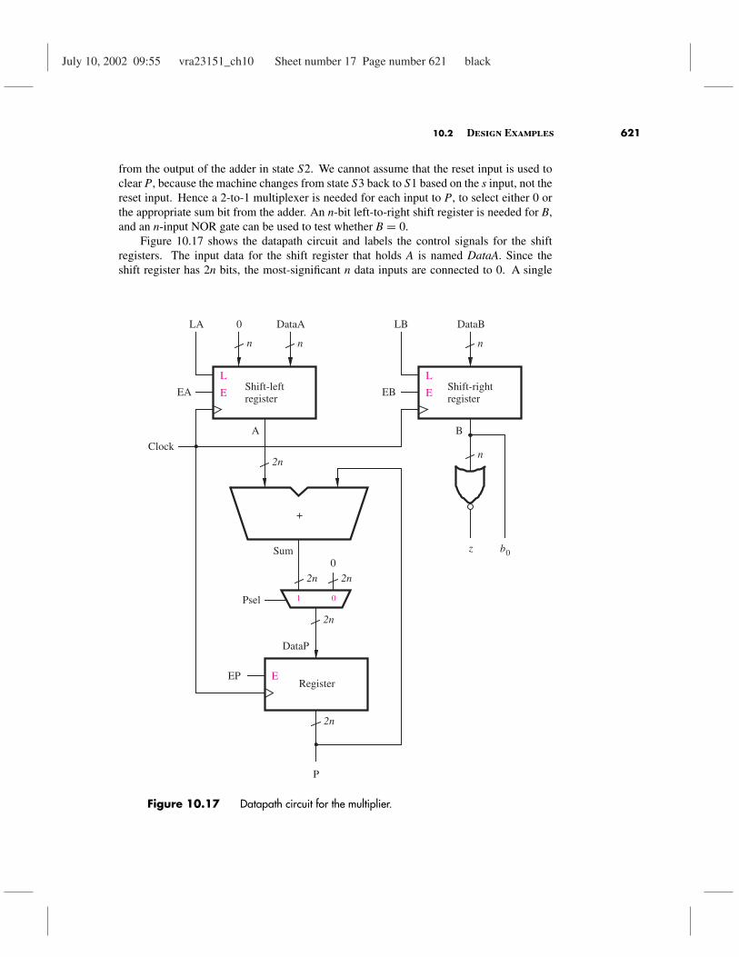
from the output of the adder in state S2. We cannot assume that the reset input is used toclear P, because the machine changes from state S3 back to S1 based on the s input, not thereset input. Hence a 2-to-1 multiplexer is needed for each input to P, to select either 0 orthe appropriate sum bit from the adder. An n-bit left-to-right shift register is needed for B,and an n-input NOR gate can be used to test whether B = 0.
Figure 10.17 shows the datapath circuit and labels the control signals for the shiftregisters. The input data for the shift register that holds A is named DataA. Since theshift register has 2n bits, the most-significant n data inputs are connected to 0. A single
E
L
E
L
E
0 DataALA
EA
A
Clock
P
DataP
RegisterEP
Sum0
z
B
b0
DataBLB
EB
+
2n
n n
Shift-leftregister
Shift-rightregister
n
n
2n 2n
Psel 1 0
2n
2n
Figure 10.17 Datapath circuit for the multiplier.
July 10, 2002 09:55 vra23151_ch10 Sheet number 18 Page number 622 black
622 C H A P T E R 10 • Digital System Design
multiplexer symbol is shown connected to the register that holds P. This symbol represents2n 2-to-1 multiplexers that are each controlled by the Psel signal.
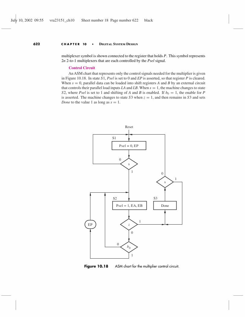
Control CircuitAn ASM chart that represents only the control signals needed for the multiplier is given
in Figure 10.18. In state S1, Psel is set to 0 and EP is asserted, so that register P is cleared.When s = 0, parallel data can be loaded into shift registers A and B by an external circuitthat controls their parallel load inputs LA and LB. When s = 1, the machine changes to stateS2, where Psel is set to 1 and shifting of A and B is enabled. If b0 = 1, the enable for Pis asserted. The machine changes to state S3 when z = 1, and then remains in S3 and setsDone to the value 1 as long as s = 1.
EP z
b0
Reset
S3
0
1
0
1s
0
1
Done
Psel 0= EP,
s0
1
S1
S2
Psel 1= EA EB, ,
Figure 10.18 ASM chart for the multiplier control circuit.
July 10, 2002 09:55 vra23151_ch10 Sheet number 19 Page number 623 black
10.2 Design Examples 623
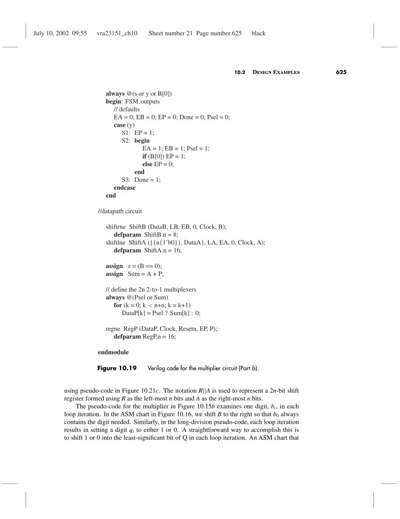
Verilog CodeVerilog code for the multiplier is given in Figure 10.19. The number of bits in A and
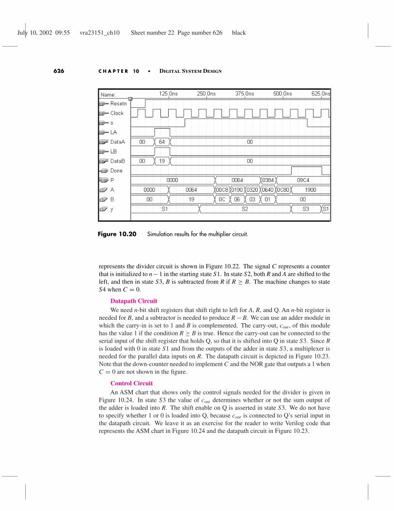
B is set by the parameter n. For registers that are 2n bits wide, the number of bits is set ton + n. By changing the value of the parameters, the code can be used for numbers of anysize. The always blocks labeled State_table and State_ flipflops define the state transitionsand state flip-flops, respectively. The control circuit outputs are specified in the alwaysblock labeled FSM_outputs. The parallel data input on the shift register A is 2n bits wide,but DataA is only n bits wide. Hence the concatenate operation {{n{1’b0}}, DataA} isused to prepend n zeros onto DataA for loading into the shift register. The multiplexerneeded for register P is defined using a for loop that defines 2n 2-to-1 multiplexers. Figure10.20 gives a simulation result for the circuit generated from the code. After the circuit isreset, LA and LB are set to 1, and the numbers to be multiplied are placed on the DataA andDataB inputs. After s is set to 1, the FSM (y) changes to state S2, where it remains untilB = 0. For each clock cycle in state S2, A is shifted to the left, and B is shifted to the right.In three of the clock cycles in state S2, the contents of A are added to P, corresponding tothe three bits in B that have the value 1. When B = 0, the FSM changes to state S3 and Pcontains the correct product, which is (64)16 × (19)16 = (9C4)16. The decimal equivalentof this result is 100× 25 = 2500.
The number of clock cycles that the circuit requires to generate the final product isdetermined by the left-most digit in B that is 1. It is possible to reduce the number of clockcycles needed by using more complex shift registers for A and B. If the two right-most bitsin B are both 0, then both A and B could be shifted by two bit positions in one clock cycle.Similarly, if the three lowest digits in B are 0, then a three bit-position shift can be done,and so on. A shift register that can shift by multiple bit positions at once can be built usinga barrel shifter. We leave it as an exercise for the reader to modify the multiplier to makeuse of a barrel shifter.
10.2.4 Divider
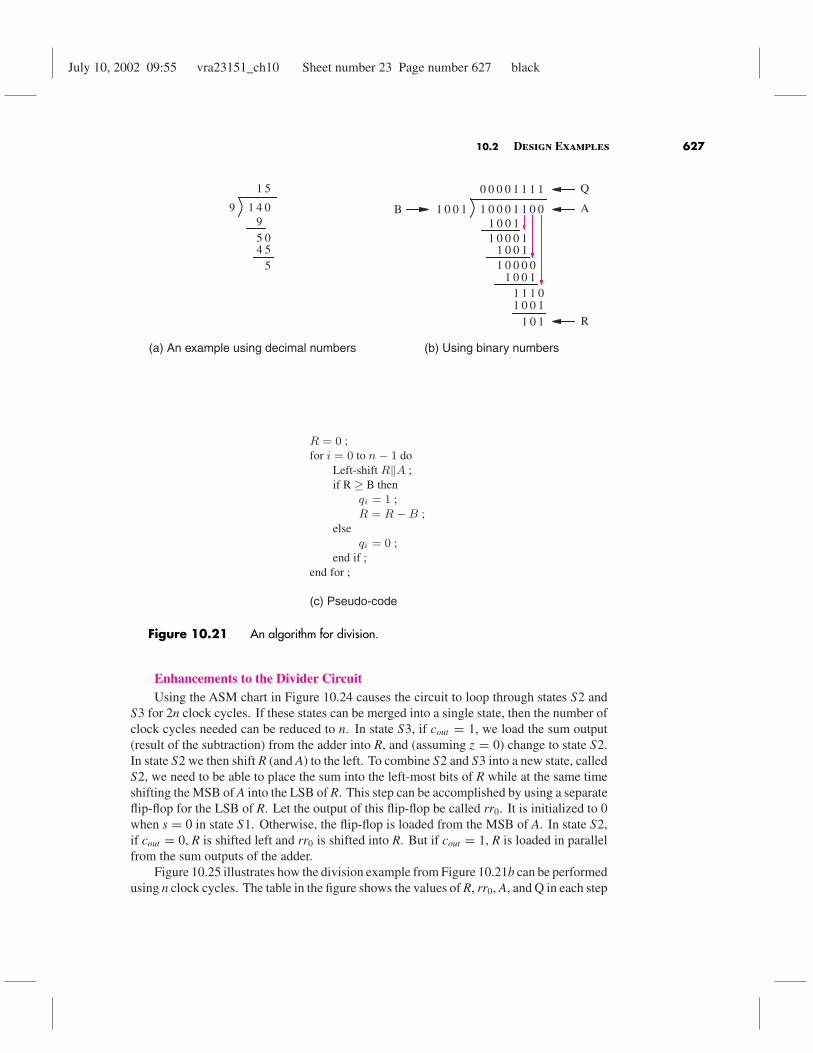
The preceding example implements the traditional method of performing multiplication byhand. In this example we will design a circuit that implements the traditional long-handdivision. Figure 10.21a gives an example of long-hand division. The first step is to try todivide the divisor 9 into the first digit of the dividend 1, which does not work. Next, we tryto divide 9 into 14, and determine that 1 is the first digit in the quotient. We perform thesubtraction 14 − 9 = 5, bring down the last digit from the dividend to form 50, and thendetermine that the next digit in the quotient is 5. The remainder is 50 − 45 = 5, and thequotient is 15. Using binary numbers, as illustrated in Figure 10.21b, involves the sameprocess, with the simplification that each digit of the quotient can be only 0 or 1.
Given two unsigned n-bit numbers A and B, we wish to design a circuit that producestwo n-bit outputs Q and R, where Q is the quotient A/B and R is the remainder. Theprocedure illustrated in Figure 10.21b can be implemented by shifting the digits in A tothe left, one digit at a time, into a shift register R. After each shift operation, we compareR with B. If R ≥ B, a 1 is placed in the appropriate bit position in the quotient and B issubtracted from R. Otherwise, a 0 bit is placed in the quotient. This algorithm is described

July 10, 2002 09:55 vra23151_ch10 Sheet number 20 Page number 624 black
624 C H A P T E R 10 • Digital System Design
module multiply (Clock, Resetn, LA, LB, s, DataA, DataB, P, Done);parameter n = 8;input Clock, Resetn, LA, LB, s;input [n 1:0] DataA, DataB;output [n+n 1:0] P;output Done;wire z;reg [n+n 1:0] A, DataP;wire [n+n 1:0] Sum;reg [1:0] y, Y;reg [n 1:0] B;reg Done, EA, EB, EP, Psel;integer k;
// control circuit
parameter S1 = 2’b00, S2 = 2’b01, S3 = 2’b10;
always @(s or y or z)begin: State table
case (y)S1: if (s == 0) Y = S1;
else Y = S2;S2: if (z == 0) Y = S2;
else Y = S3;S3: if (s == 1) Y = S3;
else Y = S1;default: Y = 2’bxx;
endcaseend
always @(posedge Clock or negedge Resetn)begin: State flipflops
if (Resetn == 0)y <= S1;
elsey <= Y;
end
. . . continued in Part b.
Figure 10.19 Verilog code for the multiplier circuit (Part a).
July 10, 2002 09:55 vra23151_ch10 Sheet number 21 Page number 625 black
10.2 Design Examples 625
always @(s or y or B[0])begin: FSM outputs
// defaultsEA = 0; EB = 0; EP = 0; Done = 0; Psel = 0;case (y)
S1: EP = 1;S2: begin
EA = 1; EB = 1; Psel = 1;if (B[0]) EP = 1;else EP = 0;
endS3: Done = 1;
endcaseend
//datapath circuit
shiftrne ShiftB (DataB, LB, EB, 0, Clock, B);defparam ShiftB.n = 8;
shiftlne ShiftA ({{n{1’b0}}, DataA}, LA, EA, 0, Clock, A);defparam ShiftA.n = 16;
assign z = (B == 0);assign Sum = A + P;
// define the 2n 2-to-1 multiplexersalways @(Psel or Sum)
for (k = 0; k < n+n; k = k+1)DataP[k] = Psel ? Sum[k] : 0;
regne RegP (DataP, Clock, Resetn, EP, P);defparam RegP.n = 16;
endmodule
Figure 10.19 Verilog code for the multiplier circuit (Part b).
using pseudo-code in Figure 10.21c. The notation R||A is used to represent a 2n-bit shiftregister formed using R as the left-most n bits and A as the right-most n bits.
The pseudo-code for the multiplier in Figure 10.15b examines one digit, bi, in eachloop iteration. In the ASM chart in Figure 10.16, we shift B to the right so that b0 alwayscontains the digit needed. Similarly, in the long-division pseudo-code, each loop iterationresults in setting a digit qi to either 1 or 0. A straightforward way to accomplish this isto shift 1 or 0 into the least-significant bit of Q in each loop iteration. An ASM chart that
July 10, 2002 09:55 vra23151_ch10 Sheet number 22 Page number 626 black
626 C H A P T E R 10 • Digital System Design
Figure 10.20 Simulation results for the multiplier circuit.
represents the divider circuit is shown in Figure 10.22. The signal C represents a counterthat is initialized to n− 1 in the starting state S1. In state S2, both R and A are shifted to theleft, and then in state S3, B is subtracted from R if R ≥ B. The machine changes to stateS4 when C = 0.
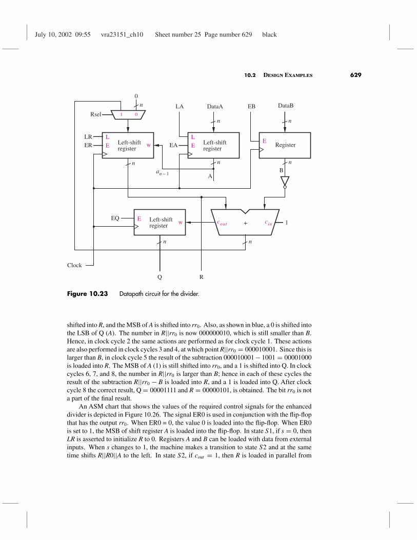
Datapath CircuitWe need n-bit shift registers that shift right to left for A, R, and Q. An n-bit register is
needed for B, and a subtractor is needed to produce R− B. We can use an adder module inwhich the carry-in is set to 1 and B is complemented. The carry-out, cout , of this modulehas the value 1 if the condition R ≥ B is true. Hence the carry-out can be connected to theserial input of the shift register that holds Q, so that it is shifted into Q in state S3. Since Ris loaded with 0 in state S1 and from the outputs of the adder in state S3, a multiplexer isneeded for the parallel data inputs on R. The datapath circuit is depicted in Figure 10.23.Note that the down-counter needed to implement C and the NOR gate that outputs a 1 whenC = 0 are not shown in the figure.
Control CircuitAn ASM chart that shows only the control signals needed for the divider is given in
Figure 10.24. In state S3 the value of cout determines whether or not the sum output ofthe adder is loaded into R. The shift enable on Q is asserted in state S3. We do not haveto specify whether 1 or 0 is loaded into Q, because cout is connected to Q’s serial input inthe datapath circuit. We leave it as an exercise for the reader to write Verilog code thatrepresents the ASM chart in Figure 10.24 and the datapath circuit in Figure 10.23.
July 10, 2002 09:55 vra23151_ch10 Sheet number 23 Page number 627 black
10.2 Design Examples 627
9 1 4 095 04 5
5
1 5
1 0 0
1 01 0
0 1 1 0 01 0 0 1
0 0 0 0 1 1 1 1
1 0 0 10 0 1
0 11 0 0 0 0
1 0 0 11 1 1 01 0 0 1
1 0 1
Q
AB
R
(a) An example using decimal numbers (b) Using binary numbers
R = 0 ;for i = 0 to n − 1 do
Left-shift R‖A ;if R ≥ B then
qi = 1 ;R = R − B ;
elseqi = 0 ;
end if ;end for ;
(c) Pseudo-code
Figure 10.21 An algorithm for division.
Enhancements to the Divider CircuitUsing the ASM chart in Figure 10.24 causes the circuit to loop through states S2 and
S3 for 2n clock cycles. If these states can be merged into a single state, then the number ofclock cycles needed can be reduced to n. In state S3, if cout = 1, we load the sum output(result of the subtraction) from the adder into R, and (assuming z = 0) change to state S2.In state S2 we then shift R (and A) to the left. To combine S2 and S3 into a new state, calledS2, we need to be able to place the sum into the left-most bits of R while at the same timeshifting the MSB of A into the LSB of R. This step can be accomplished by using a separateflip-flop for the LSB of R. Let the output of this flip-flop be called rr0. It is initialized to 0when s = 0 in state S1. Otherwise, the flip-flop is loaded from the MSB of A. In state S2,if cout = 0, R is shifted left and rr0 is shifted into R. But if cout = 1, R is loaded in parallelfrom the sum outputs of the adder.
Figure 10.25 illustrates how the division example from Figure 10.21b can be performedusing n clock cycles. The table in the figure shows the values of R, rr0, A, and Q in each step

July 10, 2002 09:55 vra23151_ch10 Sheet number 24 Page number 628 black
628 C H A P T E R 10 • Digital System Design
R B≥ ?
R 0← C n 1–←,
s0 1
S1
S2
0
Load ALoad B
Shift left R||A
C C 1–←
Shift 0 into Q Shift 1 into QR R B–←
C 0= ?
1
1 0
S3
Reset
Done
S4
0
1s
Figure 10.22 ASM chart for the divider.
of the division. In the datapath circuit in Figure 10.23, we use a separate shift register for Q.This register is not actually needed, because the digits in the quotient can be shifted into theleast-significant bit of the register used for A. In Figure 10.25 the digits of Q that are shiftedinto A are shown in blue. The first row in the table represents loading of initial data intoregisters A (and B) and clearing R and rr0 to 0. In the second row of the table, labeled clockcycle 0, the diagonal blue arrow shows that the left-most bit of A (1) is shifted into rr0. Thenumber in R||rr0 is now 000000001, which is smaller than B (1001). In clock cycle 1, rr0 is
July 10, 2002 09:55 vra23151_ch10 Sheet number 25 Page number 629 black
10.2 Design Examples 629
ELE
LE
DataB
LRER
EQ
Clock
Q
Register
EB
0
R
DataALA
EA
+E cout cin 1
B
w
Rsel
n
Left-shiftregister
n
Left-shiftregister
n n
nn
nn
Left-shiftregister
an 1– A
w
01
Figure 10.23 Datapath circuit for the divider.
shifted into R, and the MSB of A is shifted into rr0. Also, as shown in blue, a 0 is shifted intothe LSB of Q (A). The number in R||rr0 is now 000000010, which is still smaller than B.Hence, in clock cycle 2 the same actions are performed as for clock cycle 1. These actionsare also performed in clock cycles 3 and 4, at which point R||rr0 = 000010001. Since this islarger than B, in clock cycle 5 the result of the subtraction 000010001− 1001 = 00001000is loaded into R. The MSB of A (1) is still shifted into rr0, and a 1 is shifted into Q. In clockcycles 6, 7, and 8, the number in R||rr0 is larger than B; hence in each of these cycles theresult of the subtraction R||rr0 − B is loaded into R, and a 1 is loaded into Q. After clockcycle 8 the correct result, Q= 00001111 and R = 00000101, is obtained. The bit rr0 is nota part of the final result.
An ASM chart that shows the values of the required control signals for the enhanceddivider is depicted in Figure 10.26. The signal ER0 is used in conjunction with the flip-flopthat has the output rr0. When ER0 = 0, the value 0 is loaded into the flip-flop. When ER0is set to 1, the MSB of shift register A is loaded into the flip-flop. In state S1, if s = 0, thenLR is asserted to initialize R to 0. Registers A and B can be loaded with data from externalinputs. When s changes to 1, the machine makes a transition to state S2 and at the sametime shifts R||R0||A to the left. In state S2, if cout = 1, then R is loaded in parallel from
July 10, 2002 09:55 vra23151_ch10 Sheet number 26 Page number 630 black
630 C H A P T E R 10 • Digital System Design
Rsel 0= LR LC, ,
s0 1
S1
S2
Done
s
EQ Rsel 1= EC, ,
LR
1 0
S4
S3
Reset
ER EA,
cout
z
1
010
Figure 10.24 ASM chart for the divider control circuit.
the sum outputs of the adder. At the same time, R0||A is shifted left (rr0 is not shifted intoR in this case). If cout = 0, then R||R0||A is shifted left. The ASM chart shows how theparallel-load and enable inputs on the registers have to be controlled to achieve the desiredoperation.
The datapath circuit for the enhanced divider is illustrated in Figure 10.27. As discussedfor Figure 10.25, the digits of the quotient Q are shifted into register A. Note that one ofthe n-bit data inputs on the adder module is composed of the n− 1 least-significant bits inregister R concatenated with bit rr0 on the right.
Verilog CodeFigure 10.28 shows Verilog code that represents the enhanced divider. The parameter n
sets the number of bits in the operands. The State_table, State_ flipflops, and FSM_outputs
July 10, 2002 09:55 vra23151_ch10 Sheet number 27 Page number 631 black
10.2 Design Examples 631
Load A, B 0001
0011
0123 1
00
000
456 0 07
10001100
Clock cycle
0 08
0
A/Q
0110
1100
000
000
0 0
0 0
1000
0000
000
000
0 1
1 1
00000011
1
0 00 0 1 1 1 1
rr0R
0000
0000
000
000
0 0
00000000
0 00
0000
0000
011
100
1 0
0 1
0001
0010
000
000
0 0
1 1
01000110
0
0 00 0 1 0 1 0
00000000
0
0
1 0 0 0 1 1 0 01 0 0 1 AB
Shift left
Subtract, Q0 1←
Shift left, Q0 0←Shift left, Q0 0←Shift left, Q0 0←
Subtract, Q0 1←Subtract, Q0 1←Subtract, Q0 1←
Shift left, Q0 0←
Figure 10.25 An example of division using n = 8 clock cycles.
always blocks describe the control circuit, as in the previous examples. The shift registersand counters in the datapath circuit are instantiated at the bottom of the code. The signalrr0 in Figure 10.25 is represented in the code by the signal R0. This signal is implementedas the output of the muxdff component; the code for this subcircuit is shown in Figure 7.52.Note that the adder that produces the Sum signal has one input defined as the concatenationof R with R0. The multiplexer needed for the input to R is represented by the DataR signal.This multiplexer is defined in the last statement of the code.
A simulation result for the circuit produced from the code is given in Figure 10.29. Thedata A = A6 and B = 8 is loaded, and then s is set to 1. The circuit changes to state S2and concurrently shifts R, R0, and A to the left. The output of the shift register that holds Ais labeled Q in the simulation results because this shift register contains the quotient whenthe division operation is complete. On the first three active clock edges in state S2, thenumber represented by R||R0 is less than the number in B (8); hence R||R0||A is shiftedleft on each clock edge, and 0 is shifted into Q. In the fourth consecutive clock cycle forwhich the FSM has been in state S2, the contents of R are 00000101 = (5)10, and R0 is0; hence R||R0 = 000001010 = (10)10. On the next active clock edge, the output of theadder, which is 10− 8 = 2, is loaded into R, and 1 is shifted into Q. After n clock cycles instate S2, the circuit changes to state S3, and the correct result, Q= 14 = (20)10 and R = 6,is obtained.
10.2.5 Arithmetic Mean
Assume that k n-bit numbers are stored in a set of registers R0, . . . , Rk−1. We wish to designa circuit that computes the mean M of the numbers in the registers. The pseudo-code for asuitable algorithm is shown in Figure 10.30a. Each iteration of the loop adds the contentsof one of the registers, denoted Ri, to a Sum variable. After the sum is computed, M isobtained as Sum/k. We assume that integer division is used, so a remainder R, not shownin the code, is produced as well.

July 10, 2002 09:55 vra23151_ch10 Sheet number 28 Page number 632 black
632 C H A P T E R 10 • Digital System Design
Rsel 0= LC ER, ,
s0 1
S1
S2
LR
1 0
Reset
EA, ER0
cout
z
1
0
ER ER0 EA Rsel 1=, , ,
LR ECDone
s
S3
10
Figure 10.26 ASM chart for the enhanced divider control circuit.
An ASM chart is given in Figure 10.30b. While the start input, s, is 0, the registerscan be loaded from external inputs. When s becomes 1, the machine changes to state S2,where it remains while C �= 0, and computes the summation (C is a counter that representsi in Figure 10.30a). When C = 0, the machine changes to state S3 and computes M =Sum/k. From the previous example, we know that the division operation requires multipleclock cycles, but we have chosen not to indicate this in the ASM chart. After computingthe division operation, state S4 is entered and Done is set to 1.
Datapath CircuitThe datapath circuit for this task is more complex than in our previous examples. It is
depicted in Figure 10.31. We need a register with an enable input to hold Sum. For simpli-
July 10, 2002 09:55 vra23151_ch10 Sheet number 29 Page number 633 black
10.2 Design Examples 633
E
LE
LE
DataB
LRER
ClockRegister
EB
0
R
DataALA
EA
+cout cin 1
B
w
Rsel
n
Left-shiftregister
n
Left-shiftregister
n n
nn
n
qn 1–
Q
01
DQ
Q
ER0
0
1
0
n 1–
n
rn 2– … r0
w
n n
rr0
Figure 10.27 Datapath circuit for the enhanced divider.
city, assume that the sum can be represented in n bits without overflowing. A multiplexer isrequired on the data inputs on the Sum register, to select 0 in state S1 and the sum outputsof an adder in state S2. The Sum register provides one of the data inputs to the adder. Theother input has to be selected from the data outputs of one of the k registers. One wayto select among the registers is to connect them to the data inputs of a k-to-1 multiplexerthat is connected to the adder. The select lines on the multiplexer can be controlled by the

July 10, 2002 09:55 vra23151_ch10 Sheet number 30 Page number 634 black
634 C H A P T E R 10 • Digital System Design
module divider (Clock, Resetn, s, LA, EB, DataA, DataB, R, Q, Done);parameter n = 8, logn = 3;input Clock, Resetn, s, LA, EB;input [n 1:0] DataA, DataB;output [n 1:0] R, Q;output Done;wire Cout, z;wire [n 1:0] DataR;wire [n:0] Sum;reg [1:0] y, Y;reg [n 1:0] A, B;reg [logn 1:0] Count;reg Done, EA, Rsel, LR, ER, ER0, LC, EC, R0;integer k;
// control circuit
parameter S1 = 2’b00, S2 = 2’b01, S3 = 2’b10;
always @(s or y or z)begin: State table
case (y)S1: if (s == 0) Y = S1;
else Y = S2;S2: if (z == 0) Y = S2;
else Y = S3;S3: if (s == 1) Y = S3;
else Y = S1;default: Y = 2’bxx;
endcaseend
always @(posedge Clock or negedge Resetn)begin: State flipflops
if (Resetn == 0)y <= S1;
elsey <= Y;
end
. . . continued in Part b.
Figure 10.28 Verilog code for the divider circuit (Part a).

July 10, 2002 09:55 vra23151_ch10 Sheet number 31 Page number 635 black
10.2 Design Examples 635
always @(y or s or Cout or z)begin: FSM outputs
// defaultsLR = 0; ER = 0; ER0 = 0; LC = 0; EC = 0; EA = 0;Rsel = 0; Done = 0;case (y)
S1: beginLC = 1; ER = 1;if (s == 0)begin
LR = 1; ER0 = 0;endelsebegin
LR = 0; EA = 1; ER0 = 1;end
endS2: begin
Rsel = 1; ER = 1; ER0 = 1; EA = 1;if (Cout) LR = 1;else LR = 0;if (z == 0) EC = 1;else EC = 0;
endS3: Done = 1;
endcaseend
. . . continued in Part c.
Figure 10.28 Verilog code for the divider circuit (Part b).
counter C. To compute the division operation, we can use the divider circuit designed insection 10.2.4.
The circuit in Figure 10.31 is based on k = 4, but the same circuit structure can beused for larger values of k. Note that the enable inputs on the registers R0 through R3 areconnected to the outputs of a 2-to-4 decoder that has the two-bit input RAdd, which standsfor “register address.” The decoder enable input is driven by the ER signal. All registersare loaded from the same input lines, Data. Since k = 4, we could perform the divisionoperation simply by shifting Sum two bits to the right, which can be done in one clock cyclewith a shift register that shifts by two digits. To obtain a more general circuit that worksfor any value of k, we use the divider circuit designed in section 10.2.4.

July 10, 2002 09:55 vra23151_ch10 Sheet number 32 Page number 636 black
636 C H A P T E R 10 • Digital System Design
// datapath circuit
regne RegB (DataB, Clock, Resetn, EB, B);defparam RegB.n = n;
shiftlne ShiftR (DataR, LR, ER, R0, Clock, R);defparam ShiftR.n = n;
muxdff FF R0 (0, A[n−1], ER0, Clock, R0);shiftlne ShiftA (DataA, LA, EA, Cout, Clock, A);
defparam ShiftA.n = n;assign Q = A;downcount Counter (Clock, EC, LC, Count);
defparam Counter.n = logn;
assign z = (Count == 0);assign Sum = {R, R0} + ( B + 1);assign Cout = Sum[n];
// define the n 2-to-1 multiplexersassign DataR = Rsel ? Sum : 0;
endmodule
Figure 10.28 Verilog code for the divider circuit (Part c).
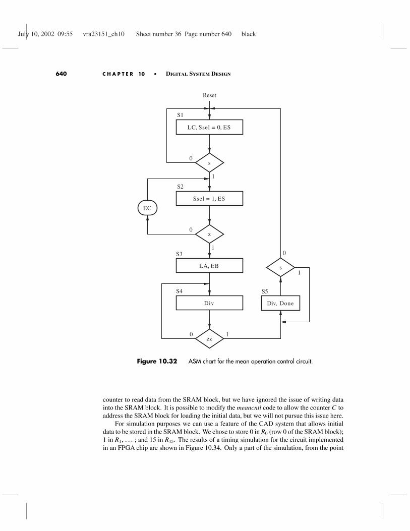
Control CircuitFigure 10.32 gives an ASM chart for the FSM needed to control the circuit in Figure
10.31. While in state S1, data can be loaded into registers R0, . . . , Rk−1. But no controlsignals have to be asserted for this purpose, because the registers are loaded under controlof the ER and RAdd inputs, as discussed above. When s = 1, the FSM changes to stateS2, where it asserts the enable ES on the Sum register and allows C to decrement. Whenthe counter reaches 0 (z = 1), the machine enters state S3, where it asserts the LA and EBsignals to load the Sum and k into the A and B inputs of the divider circuit, respectively. TheFSM then enters state S4 and asserts the Div signal to start the division operation. Whenit is finished, the divider circuit sets zz = 1, and the FSM moves to state S5. The mean Mappears on the Q and R outputs of the divider circuit. The Div signal must still be assertedin state S5 to prevent the divider circuit from reinitializing its registers. Note that in theASM chart in Figure 10.30b, only one state is shown for computing M = Sum/k, but inFigure 10.32, states S3 and S4 are used for this purpose. It is possible to combine states S3and S4, which we will leave as an exercise for the reader (problem 10.6).
Alternative Datapath CircuitsIn Figure 10.31 registers R0, . . . , Rk−1 are connected to the adder using a multiplexer.
Another way to achieve the desired connection is to add tri-state buffers to the outputs of thek registers and to connect all tri-state buffers for a given bit position to the corresponding

July 10, 2002 09:55 vra23151_ch10 Sheet number 33 Page number 637 black
10.2 Design Examples 637
Figure 10.29 Simulation results for the divider circuit.
input of the adder. The down-counter C can be used to enable each tri-state buffer at theproper time (when the FSM is in state S2), by connecting a 2-to-4 decoder to the outputsof the counter and using one output of the decoder to enable each tri-state buffer. We willshow an example of using tri-states buffers in this manner in Figure 10.42.
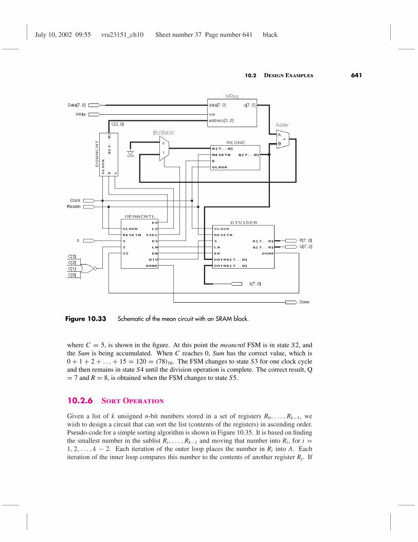
For large values of k, it is preferable to use an SRAM block with k rows and n columns,instead of using k registers. Predefined modules that represent SRAM blocks are usuallyprovided by CAD tools. If the circuit being designed is to be implemented in a customchip, then the CAD tools ensure that the desired SRAM block is included on the chip.Some PLDs include SRAM blocks that can be configured to implement various numbers ofrows and columns. The CAD system that accompanies the book provides the lpm_ram_dqmodule, which is a part of the LPM standard library.
Figure 10.33 gives a schematic diagram for the arithmetic mean circuit, using theparameters k = 16 and n = 8. This schematic was created using the CAD tools thataccompany the book. Four of the graphical symbols in the schematic represent subcircuitsdescribed using Verilog code, namely downcnt, regne, divider, and meancntl. The codefor the divider subcircuit is shown in Figure 10.28. The meancntl subcircuit represents theFSM in Figure 10.32. The Verilog code for this FSM is not shown. The schematic alsoincludes a multiplexer connected to the Sum register, an adder, and a NOR gate that detectswhen the counter C reaches 0. The outputs of the counter provide the address inputs to theSRAM block, called MReg.
The SRAM block has 16 rows and eight columns. In Figure 10.31 a decoder controlsthe loading of data into each of the k registers. To read the data from the registers, thecounter C is used. To keep the schematic in Figure 10.33 simple, we have included the
July 10, 2002 09:55 vra23151_ch10 Sheet number 34 Page number 638 black
638 C H A P T E R 10 • Digital System Design
Sum = 0 ;for i = k − 1 down to 0 do
Sum = Sum +Ri
end for ;M = Sum ÷ k ;
(a) Pseudo-code
Sum 0← C k 1–←,
s0
1
S1
S2
Done
s
Reset
1
0
Sum Sum Ri+←
S4
C 0= ?
M Sum k⁄←
C C 1–←
0
1S3
Load registers
(b) ASM chart
Figure 10.30 An algorithm for finding the mean of k numbers.

July 10, 2002 09:55 vra23151_ch10 Sheet number 35 Page number 639 black
10.2 Design Examples 639
ERegister
+
ERegister
ERegister
ERegister
ERRAdd
EL Down-counterE
Register
B EB A LA
R Q Done
sDivider
ES
0
Ssel
ECLC
Div
k EB
LA
zz
Sum
M
Data
Clock
z
k 1–
n
n
n
nn
n
n
w0 En
y0
w1
y1 y2 y3
2-to-4
Figure 10.31 Datapath circuit for the mean operation.
July 10, 2002 09:55 vra23151_ch10 Sheet number 36 Page number 640 black
640 C H A P T E R 10 • Digital System Design
LC Ssel 0= ES, ,
s0
1
S1
S2
Div, Done
s
Reset
1
0
Ssel 1= ES,
S5
LA EB,
EC
0
1S3
z
Div
zz
S4
0 1
Figure 10.32 ASM chart for the mean operation control circuit.
counter to read data from the SRAM block, but we have ignored the issue of writing datainto the SRAM block. It is possible to modify the meancntl code to allow the counter C toaddress the SRAM block for loading the initial data, but we will not pursue this issue here.
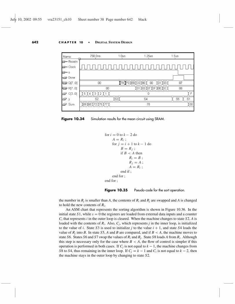
For simulation purposes we can use a feature of the CAD system that allows initialdata to be stored in the SRAM block. We chose to store 0 in R0 (row 0 of the SRAM block);1 in R1, . . . ; and 15 in R15. The results of a timing simulation for the circuit implementedin an FPGA chip are shown in Figure 10.34. Only a part of the simulation, from the point
July 10, 2002 09:55 vra23151_ch10 Sheet number 37 Page number 641 black
10.2 Design Examples 641
Figure 10.33 Schematic of the mean circuit with an SRAM block.
where C = 5, is shown in the figure. At this point the meancntl FSM is in state S2, andthe Sum is being accumulated. When C reaches 0, Sum has the correct value, which is0 + 1 + 2 + . . . + 15 = 120 = (78)16. The FSM changes to state S3 for one clock cycleand then remains in state S4 until the division operation is complete. The correct result, Q= 7 and R = 8, is obtained when the FSM changes to state S5.
10.2.6 Sort Operation
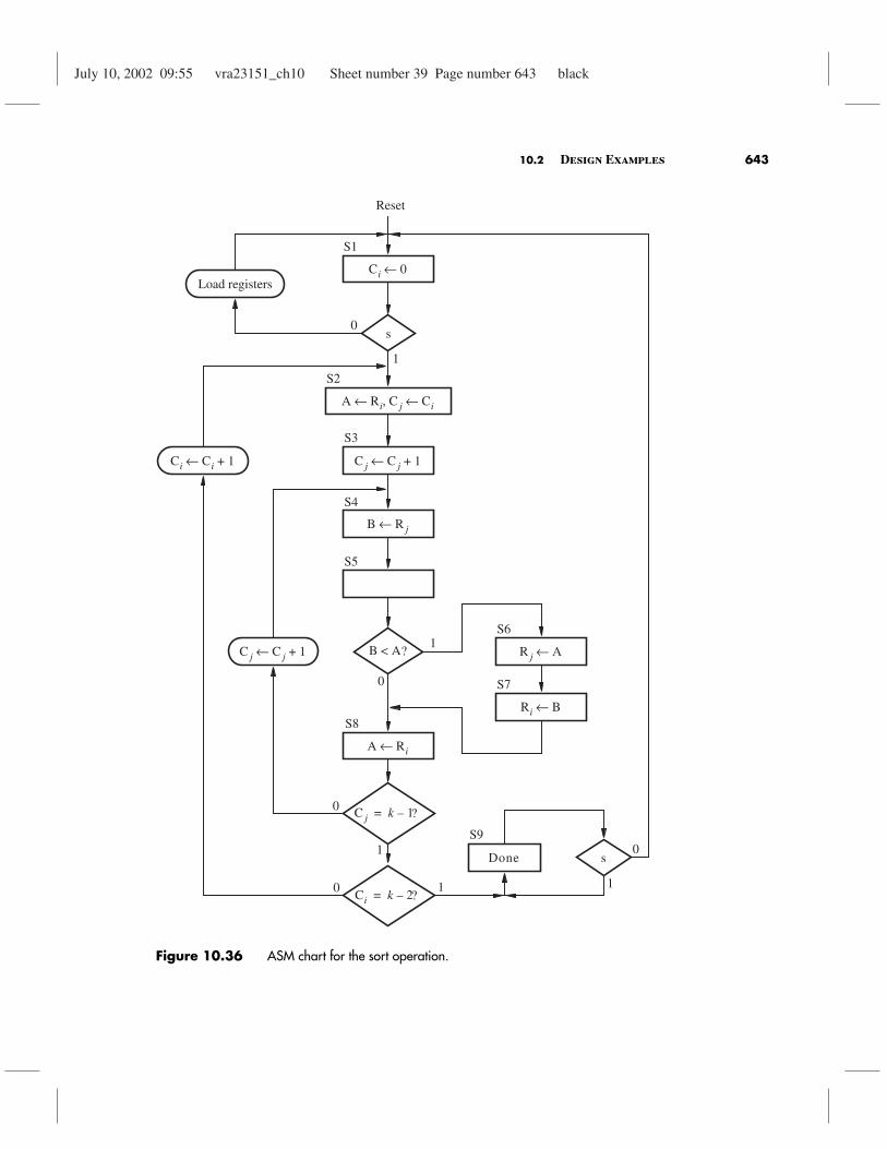
Given a list of k unsigned n-bit numbers stored in a set of registers R0, . . . , Rk−1, wewish to design a circuit that can sort the list (contents of the registers) in ascending order.Pseudo-code for a simple sorting algorithm is shown in Figure 10.35. It is based on findingthe smallest number in the sublist Ri, . . . , Rk−1 and moving that number into Ri, for i =1, 2, . . . , k − 2. Each iteration of the outer loop places the number in Ri into A. Eachiteration of the inner loop compares this number to the contents of another register Rj. If
July 10, 2002 09:55 vra23151_ch10 Sheet number 38 Page number 642 black
642 C H A P T E R 10 • Digital System Design
Figure 10.34 Simulation results for the mean circuit using SRAM.
for i = 0 to k 2 doA = Ri ;for j = i + 1 to k 1 do
B = R j ;if B < A then
Ri = B ;R j = A ;A = Ri ;
end if ;end for ;
end for ;
Figure 10.35 Pseudo-code for the sort operation.
the number in Rj is smaller than A, the contents of Ri and Rj are swapped and A is changedto hold the new contents of Ri.
An ASM chart that represents the sorting algorithm is shown in Figure 10.36. In theinitial state S1, while s = 0 the registers are loaded from external data inputs and a counterCi that represents i in the outer loop is cleared. When the machine changes to state S2, A isloaded with the contents of Ri. Also, Cj, which represents j in the inner loop, is initializedto the value of i. State S3 is used to initialize j to the value i + 1, and state S4 loads thevalue of Rj into B. In state S5, A and B are compared, and if B < A, the machine moves tostate S6. States S6 and S7 swap the values of Ri and Rj. State S8 loads A from Ri. Althoughthis step is necessary only for the case where B < A, the flow of control is simpler if thisoperation is performed in both cases. If Cj is not equal to k − 1, the machine changes fromS8 to S4, thus remaining in the inner loop. If Cj = k − 1 and Ci is not equal to k − 2, thenthe machine stays in the outer loop by changing to state S2.
July 10, 2002 09:55 vra23151_ch10 Sheet number 39 Page number 643 black
10.2 Design Examples 643
B A< ?
Ci 0←
s0
1
S1
S2
Done s
Reset
A Ri← C j Ci←,
Ci Ci 1+←
S4
S5
0
1
S3
C j C j 1+←
B R j←
R j A←
Ri B←
A Ri←
C j k 1–= ?
C j C j 1+←
Ci k 2–= ?0 1
0
1
Load registers
0
1
S9
S7
S6
S8
Figure 10.36 ASM chart for the sort operation.
July 10, 2002 09:55 vra23151_ch10 Sheet number 40 Page number 644 black
644 C H A P T E R 10 • Digital System Design
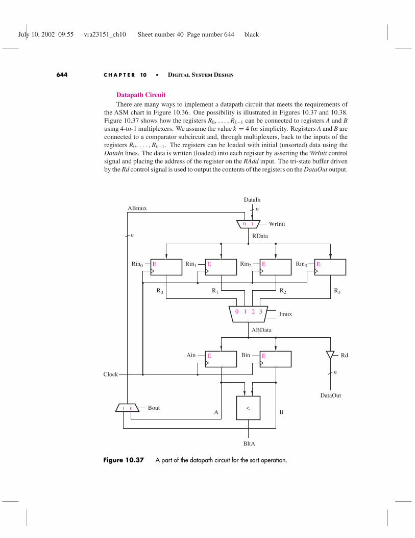
Datapath CircuitThere are many ways to implement a datapath circuit that meets the requirements of
the ASM chart in Figure 10.36. One possibility is illustrated in Figures 10.37 and 10.38.Figure 10.37 shows how the registers R0, . . . , Rk−1 can be connected to registers A and Busing 4-to-1 multiplexers. We assume the value k = 4 for simplicity. Registers A and B areconnected to a comparator subcircuit and, through multiplexers, back to the inputs of theregisters R0, . . . , Rk−1. The registers can be loaded with initial (unsorted) data using theDataIn lines. The data is written (loaded) into each register by asserting the WrInit controlsignal and placing the address of the register on the RAdd input. The tri-state buffer drivenby the Rd control signal is used to output the contents of the registers on the DataOut output.
E E E E
Clock
DataIn
WrInit
Rin3Rin2Rin1Rin0
E EBinAin
DataOut
Rd
ABData
Imux
<Bout
BltA
1 0A B
0 1
RData
R0 R1 R2 R3
0 1 2 3
ABmux n
n
n
Figure 10.37 A part of the datapath circuit for the sort operation.

July 10, 2002 09:55 vra23151_ch10 Sheet number 41 Page number 645 black
10.2 Design Examples 645
L
E
L
E
10
10
k 2–=
k 1–=
LJ
EJ
LI
EI
2-to-4 decoder
WrInit
Wr
RAdd
Clock
Csel
Int
Imux
2
Ci C j
zi
z jCmux
Rin0
Rin1
Rin2
Rin3
0
2
2
2
2
2
Counter Counter
R
R
w0 w1,
En
y0
y1
y2
y3
2
Figure 10.38 A part of the datapath circuit for the sort operation.
The signals Rin0, . . . , Rink−1 are controlled by the 2-to-4 decoder shown in Figure10.38. If Int = 1, the decoder is driven by one of the counters Ci or Cj. If Int = 0, then thedecoder is driven by the external input RAdd. The signals zi and zj are set to 1 if Ci = k− 2and Cj = k − 1, respectively. An ASM chart that shows the control signals used in thedatapath circuit is given in Figure 10.39.
Verilog CodeVerilog code for the sorting operation is presented in Figure 10.40. The FSM that
controls the sort operation is described in the same way as in previous examples, using thealways blocks State_table, State_ flipflops, and FSM_outputs. Following these blocks, thecode instantiates the registers R0 to R3, as well as A and B. The counters Ci and Cj have theinstance names OuterLoop and InnerLoop, respectively. The multiplexers with the outputsCMux and IMux are specified using the conditional operator. The 4-to-1 multiplexer inFigure 10.37 is defined by the case statement that specifies the value of the ABData signalfor each value of IMux. The 2-to-4 decoder in Figure 10.38 with the outputs Rin0, . . . , Rin3

July 10, 2002 09:55 vra23151_ch10 Sheet number 42 Page number 646 black
646 C H A P T E R 10 • Digital System Design
Csel 0= Int 1= Ain, ,
Csel 0= Int 1= Wr Bout, , ,
Csel 1= Int 1= Wr Aout, , ,
Bin Csel 1= Int 1=, ,
s0
1
S1
S2
Done s
Reset
S4
S5
0
1
S3
1
0
1
S9
S7
S6
S8
LI Int 0=,
Int 1= Csel 0= Ain LJ, , ,
EJ
BltAEJ
EI
0
1
0
z j
zi
Figure 10.39 ASM chart for the control circuit.
July 10, 2002 09:55 vra23151_ch10 Sheet number 43 Page number 647 black
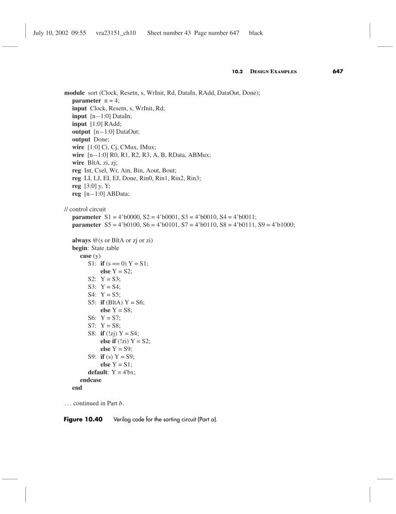
10.2 Design Examples 647
module sort (Clock, Resetn, s, WrInit, Rd, DataIn, RAdd, DataOut, Done);parameter n = 4;input Clock, Resetn, s, WrInit, Rd;input [n 1:0] DataIn;input [1:0] RAdd;output [n 1:0] DataOut;output Done;wire [1:0] Ci, Cj, CMux, IMux;wire [n 1:0] R0, R1, R2, R3, A, B, RData, ABMux;wire BltA, zi, zj;reg Int, Csel, Wr, Ain, Bin, Aout, Bout;reg LI, LJ, EI, EJ, Done, Rin0, Rin1, Rin2, Rin3;reg [3:0] y, Y;reg [n 1:0] ABData;
// control circuitparameter S1 = 4’b0000, S2 = 4’b0001, S3 = 4’b0010, S4 = 4’b0011;parameter S5 = 4’b0100, S6 = 4’b0101, S7 = 4’b0110, S8 = 4’b0111, S9 = 4’b1000;
always @(s or BltA or zj or zi)begin: State table
case (y)S1: if (s == 0) Y = S1;
else Y = S2;S2: Y = S3;S3: Y = S4;S4: Y = S5;S5: if (BltA) Y = S6;
else Y = S8;S6: Y = S7;S7: Y = S8;S8: if (!zj) Y = S4;
else if (!zi) Y = S2;else Y = S9;
S9: if (s) Y = S9;else Y = S1;
default: Y = 4'bx;endcase
end
. . . continued in Part b.
Figure 10.40 Verilog code for the sorting circuit (Part a).

July 10, 2002 09:55 vra23151_ch10 Sheet number 44 Page number 648 black
648 C H A P T E R 10 • Digital System Design
always @(posedge Clock or negedge Resetn)begin: State flipflops
if (Resetn == 0)y <= S1;
elsey <= Y;
end
always @(y or zj or zi)begin: FSM outputs
// defaultsInt = 1; Done = 0; LI = 0; LJ = 0; EI = 0; EJ = 0; Csel = 0;Wr = 0; Ain = 0; Bin = 0; Aout = 0; Bout = 0;case (y)
S1: begin LI = 1; Int = 0; endS2: begin Ain = 1; LJ = 1; endS3: EJ = 1;S4: begin Bin = 1; Csel = 1; endS5:; // no ouputs asserted in this stateS6: begin Csel = 1; Wr = 1; Aout = 1; endS7: begin Wr = 1; Bout = 1; endS8: begin
Ain = 1;if (!zj) EJ = 1;elsebegin
EJ = 0;if (!zi) EI = 1;else EI = 0;
endend
S9: Done = 1;endcase
end
. . . continued in Part c.
Figure 10.40 Verilog code for the sorting circuit (Part b).
is defined by the case statement that sets the value of the concatenated signals {Rin3, Rin2,Rin1, Rin0}. Finally, the code specifies the values of the zi and zj signals, and defines thetri-state buffers for the DataOut output.
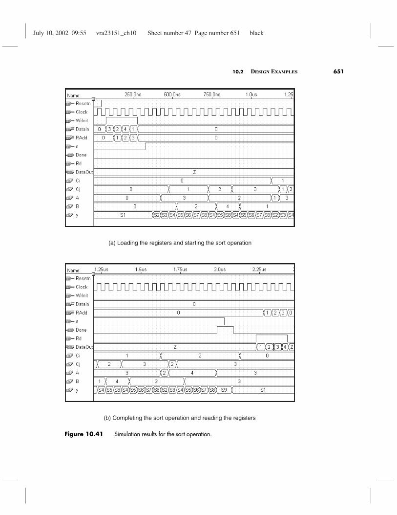
We implemented the code in Figure 10.40 in an FPGA chip. Figure 10.41 gives anexample of a simulation result. Part (a) of the figure shows the first half of the simulation,
July 10, 2002 09:55 vra23151_ch10 Sheet number 45 Page number 649 black
10.2 Design Examples 649
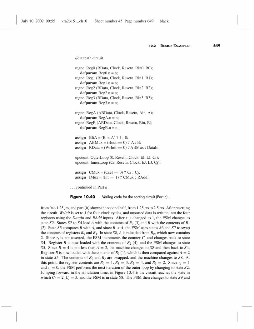
//datapath circuit
regne Reg0 (RData, Clock, Resetn, Rin0, R0);defparam Reg0.n = n;
regne Reg1 (RData, Clock, Resetn, Rin1, R1);defparam Reg1.n = n;
regne Reg2 (RData, Clock, Resetn, Rin2, R2);defparam Reg2.n = n;
regne Reg3 (RData, Clock, Resetn, Rin3, R3);defparam Reg3.n = n;
regne RegA (ABData, Clock, Resetn, Ain, A);defparam RegA.n = n;
regne RegB (ABData, Clock, Resetn, Bin, B);defparam RegB.n = n;
assign BltA = (B < A) ? 1 : 0;assign ABMux = (Bout == 0) ? A : B;assign RData = (WrInit == 0) ? ABMux : DataIn;
upcount OuterLoop (0, Resetn, Clock, EI, LI, Ci);upcount InnerLoop (Ci, Resetn, Clock, EJ, LJ, Cj);
assign CMux = (Csel == 0) ? Ci : Cj;assign IMux = (Int == 1) ? CMux : RAdd;
. . . continued in Part d.
Figure 10.40 Verilog code for the sorting circuit (Part c).
from 0 to 1.25 µs, and part (b) shows the second half, from 1.25 µs to 2.5 µs. After resettingthe circuit, WrInit is set to 1 for four clock cycles, and unsorted data is written into the fourregisters using the DataIn and RAdd inputs. After s is changed to 1, the FSM changes tostate S2. States S2 to S4 load A with the contents of R0 (3) and B with the contents of R1
(2). State S5 compares B with A, and since B < A, the FSM uses states S6 and S7 to swapthe contents of registers R0 and R1. In state S8, A is reloaded from R0, which now contains2. Since zj is not asserted, the FSM increments the counter Cj and changes back to stateS4. Register B is now loaded with the contents of R2 (4), and the FSM changes to stateS5. Since B = 4 is not less than A = 2, the machine changes to S8 and then back to S4.Register B is now loaded with the contents of R3 (1), which is then compared against A = 2in state S5. The contents of R0 and R3 are swapped, and the machine changes to S8. Atthis point, the register contents are R0 = 1, R1 = 3, R2 = 4, and R3 = 2. Since zj = 1and zi = 0, the FSM performs the next iteration of the outer loop by changing to state S2.Jumping forward in the simulation time, in Figure 10.41b the circuit reaches the state inwhich Ci = 2, Cj = 3, and the FSM is in state S8. The FSM then changes to state S9 and

July 10, 2002 09:55 vra23151_ch10 Sheet number 46 Page number 650 black
650 C H A P T E R 10 • Digital System Design
always @(WrInit or Wr or IMux)begin
case (IMux)0: ABData = R0;1: ABData = R1;2: ABData = R2;3: ABData = R3;
endcase
if (WrInit ||Wr)case (IMux)
0: {Rin3, Rin2, Rin1, Rin0} = 4’b0001;1: {Rin3, Rin2, Rin1, Rin0} = 4’b0010;2: {Rin3, Rin2, Rin1, Rin0} = 4’b0100;3: {Rin3, Rin2, Rin1, Rin0} = 4’b1000;
endcaseelse {Rin3, Rin2, Rin1, Rin0} = 4’b0000;
end
assign zi = (Ci == 2);assign zj = (Cj == 3);assign DataOut = (Rd == 0) ? ’bz : ABData;
endmodule
Figure 10.40 Verilog code for the sorting circuit (Part d ).
sets Done to the value 1. The correctly sorted data is read out of the registers by setting thesignal Rd = 1 and using the RAdd inputs to select each of the registers.
Alternative Datapath CircuitsIn Figure 10.37 we use multiplexers to connect the various registers in the datapath
circuit. Another approach is to use tri-state buffers to interconnect the registers, as illustratedin Figure 10.42. As we said in section 7.14, the set of n common wires that connect theregisters is called a bus. The circuit in Figure 10.42 has two buses, one that connects theoutputs of registers R0, . . . , R3 to the inputs of registers A and B and another that connectsthe outputs of A and B back to the inputs of R0, . . . , Rk−1. When multiplexers provide theconnection between registers, as shown in Figure 10.37, the term bus can still be used torefer to the connection between registers.
The circuit in Figure 10.42 uses the circuit in Figure 10.38 with one modification. InFigure 10.38 the IMux signal is connected to a 2-to-4 decoder that generates Rin0, . . . , Rin3.If the circuit in Figure 10.42 is used, then a second decoder connected to IMux is required
July 10, 2002 09:55 vra23151_ch10 Sheet number 47 Page number 651 black
10.2 Design Examples 651
(a) Loading the registers and starting the sort operation
(b) Completing the sort operation and reading the registers
Figure 10.41 Simulation results for the sort operation.

July 10, 2002 09:55 vra23151_ch10 Sheet number 48 Page number 652 black
652 C H A P T E R 10 • Digital System Design
E E E E
Clock
DataIn
WrInit
Rin3Rin2Rin1Rin0
E EBinAin
A B
BltABout
Aout
DataOut
Rd
Rout3Rout2Rout1Rout0
<
n
n
n n n n
n
nn
Figure 10.42 Using tri-state buffers in the datapath circuit.
to generate the control signals Rout0, . . . , Rout3. The control circuit described in the ASMchart in Figure 10.39 can be used for the datapath circuit in Figure 10.42.
We said in section 10.2.5 that for large values of k, it is better to use an SRAM blockto store the data, instead of individual registers. The sorting circuit can be changed to makeuse of an SRAM block with k rows and n columns. In this case the datapath circuit is similarto the one in Figure 10.37, but does not require the 4-to-1 multiplexers, because the dataoutputs from the SRAM block are connected directly to registers A and B. We still needto use the circuit in Figure 10.38, except that the 2-to-4 decoder is not required, becausethe IMux signal is connected to the address inputs on the SRAM block. The write input onthe SRAM block is driven by the OR gate with the inputs WrInit and Wr. Verilog code canbe written for the sorting circuit, in which a component that represents the SRAM block isinstantiated from a library of predefined modules. The code for the control circuit shownin Figure 10.40 does not have to be changed (see problem 10.11).

July 10, 2002 09:55 vra23151_ch10 Sheet number 49 Page number 653 black
10.3 Clock Synchronization 653
10.3 Clock Synchronization
In the previous section we provided several examples of circuits that contain many flip-flops.In Chapter 9 we showed that to ensure proper operation of sequential circuits it is essentialto give careful consideration to the timing aspects associated with the storage elements.This section discusses some of the timing aspects of synchronous sequential circuits.
10.3.1 Clock Skew
Figure 10.1 shows how an enable input can be used to prevent a flip-flop from changing itsstored value when an active clock edge occurs. Another way to implement the clock enablefeature is shown in Figure 10.43. The circuit uses an AND gate to force the clock input tohave the value 0 when E = 0. This circuit is simpler than the one in Figure 10.1 but cancause problems in practice. Consider a sequential circuit that has many flip-flops, some ofwhich have an enable input and others that do not. If the circuit in Figure 10.43 is used,then the flip-flops without the enable input will observe changes in the clock signal slightlyearlier than the flip-flops that have the enable input. This situation, in which the clock signalarrives at different times at different flip-flops, is known as clock skew. Figure 10.43 showsonly one possible source of clock skew. Similar problems arise in a chip in which the clocksignal is distributed to different flip-flops by wires whose lengths vary appreciably.
To understand the possible problems caused by clock skew, consider the datapathcircuit for the bit-counting example in Figure 10.11. The shift register’s LSB, a0, is usedas a control signal that determines whether or not a counter is incremented. Assume thatclock skew exists that causes the clock signal to arrive earlier at the shift-register flip-flopsthan at the counter. The clock skew may cause the shift register to be shifted before thevalue of a0 is used to cause the counter to increment. Therefore, the signal EB in Figure10.11 may fail to cause the counter to be incremented even if the value of a0 was 1.
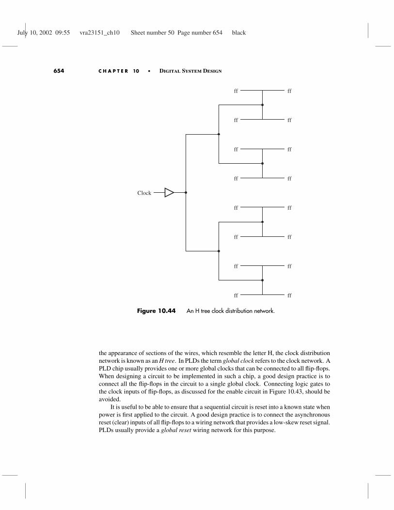
For proper operation of synchronous sequential circuits, it is essential to minimize theclock skew as much as possible. Chips that contain many flip-flops, such as PLDs, usecarefully designed networks of wires to distribute the clock signal to the flip-flops. Figure10.44 gives an example of a clock-distribution network. Each node labeled ff representsthe clock input of a flip-flop; for clarity, the flip-flops are not shown. The buffer on theleft of the figure produces the clock signal. This signal is distributed to the flip-flops suchthat the length of the wire between each flip-flop and the clock source is the same. Due to
D Q
Q
Data
Clock
E
Figure 10.43 Clock enable circuit.
July 10, 2002 09:55 vra23151_ch10 Sheet number 50 Page number 654 black
654 C H A P T E R 10 • Digital System Design
Clock
ff
ff
ff
ff
ff
ff
ff
ff
ff
ff
ff
ff
ff
ff
ff
ff
Figure 10.44 An H tree clock distribution network.
the appearance of sections of the wires, which resemble the letter H, the clock distributionnetwork is known as an H tree. In PLDs the term global clock refers to the clock network. APLD chip usually provides one or more global clocks that can be connected to all flip-flops.When designing a circuit to be implemented in such a chip, a good design practice is toconnect all the flip-flops in the circuit to a single global clock. Connecting logic gates tothe clock inputs of flip-flops, as discussed for the enable circuit in Figure 10.43, should beavoided.
It is useful to be able to ensure that a sequential circuit is reset into a known state whenpower is first applied to the circuit. A good design practice is to connect the asynchronousreset (clear) inputs of all flip-flops to a wiring network that provides a low-skew reset signal.PLDs usually provide a global reset wiring network for this purpose.
July 10, 2002 09:55 vra23151_ch10 Sheet number 51 Page number 655 black
10.3 Clock Synchronization 655
10.3.2 Flip-Flop Timing Parameters
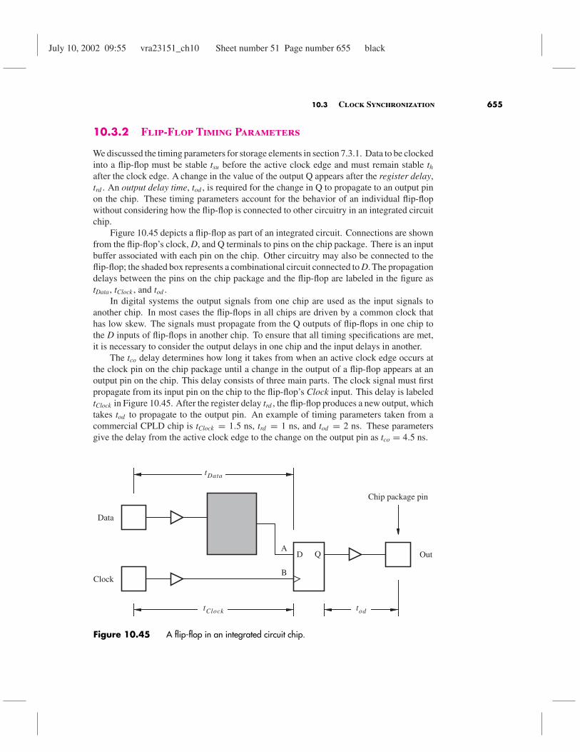
We discussed the timing parameters for storage elements in section 7.3.1. Data to be clockedinto a flip-flop must be stable tsu before the active clock edge and must remain stable thafter the clock edge. A change in the value of the output Q appears after the register delay,trd . An output delay time, tod , is required for the change in Q to propagate to an output pinon the chip. These timing parameters account for the behavior of an individual flip-flopwithout considering how the flip-flop is connected to other circuitry in an integrated circuitchip.
Figure 10.45 depicts a flip-flop as part of an integrated circuit. Connections are shownfrom the flip-flop’s clock, D, and Q terminals to pins on the chip package. There is an inputbuffer associated with each pin on the chip. Other circuitry may also be connected to theflip-flop; the shaded box represents a combinational circuit connected to D. The propagationdelays between the pins on the chip package and the flip-flop are labeled in the figure astData, tClock , and tod .
In digital systems the output signals from one chip are used as the input signals toanother chip. In most cases the flip-flops in all chips are driven by a common clock thathas low skew. The signals must propagate from the Q outputs of flip-flops in one chip tothe D inputs of flip-flops in another chip. To ensure that all timing specifications are met,it is necessary to consider the output delays in one chip and the input delays in another.
The tco delay determines how long it takes from when an active clock edge occurs atthe clock pin on the chip package until a change in the output of a flip-flop appears at anoutput pin on the chip. This delay consists of three main parts. The clock signal must firstpropagate from its input pin on the chip to the flip-flop’s Clock input. This delay is labeledtClock in Figure 10.45. After the register delay trd , the flip-flop produces a new output, whichtakes tod to propagate to the output pin. An example of timing parameters taken from acommercial CPLD chip is tClock = 1.5 ns, trd = 1 ns, and tod = 2 ns. These parametersgive the delay from the active clock edge to the change on the output pin as tco = 4.5 ns.
D Q
Data
Clock
Chip package pin
A
B
tClock
tData
Out
tod
Figure 10.45 A flip-flop in an integrated circuit chip.
July 10, 2002 09:55 vra23151_ch10 Sheet number 52 Page number 656 black
656 C H A P T E R 10 • Digital System Design
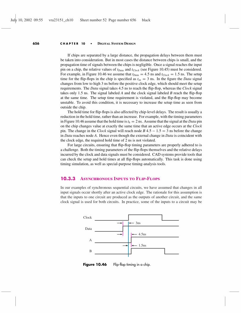
If chips are separated by a large distance, the propagation delays between them mustbe taken into consideration. But in most cases the distance between chips is small, and thepropagation time of signals between the chips is negligible. Once a signal reaches the inputpin on a chip, the relative values of tData and tClock (see Figure 10.45) must be considered.For example, in Figure 10.46 we assume that tData = 4.5 ns and tClock = 1.5 ns. The setuptime for the flip-flops in the chip is specified as tsu = 3 ns. In the figure the Data signalchanges from low to high 3 ns before the positive clock edge, which should meet the setuprequirements. The Data signal takes 4.5 ns to reach the flip-flop, whereas the Clock signaltakes only 1.5 ns. The signal labeled A and the clock signal labeled B reach the flip-flopat the same time. The setup time requirement is violated, and the flip-flop may becomeunstable. To avoid this condition, it is necessary to increase the setup time as seen fromoutside the chip.
The hold time for flip-flops is also affected by chip-level delays. The result is usually areduction in the hold time, rather than an increase. For example, with the timing parametersin Figure 10.46 assume that the hold time is th = 2 ns. Assume that the signal at the Data pinon the chip changes value at exactly the same time that an active edge occurs at the Clockpin. The change in the Clock signal will reach node B 4.5− 1.5 = 3 ns before the changein Data reaches node A. Hence even though the external change in Data is coincident withthe clock edge, the required hold time of 2 ns is not violated.
For large circuits, ensuring that flip-flop timing parameters are properly adhered to isa challenge. Both the timing parameters of the flip-flops themselves and the relative delaysincurred by the clock and data signals must be considered. CAD systems provide tools thatcan check the setup and hold times at all flip-flops automatically. This task is done usingtiming simulation, as well as special-purpose timing-analysis tools.
10.3.3 Asynchronous Inputs to Flip-Flops
In our examples of synchronous sequential circuits, we have assumed that changes in allinput signals occur shortly after an active clock edge. The rationale for this assumption isthat the inputs to one circuit are produced as the outputs of another circuit, and the sameclock signal is used for both circuits. In practice, some of the inputs to a circuit may be
Data
Clock
A
3ns
4.5ns
1.5ns
B
Figure 10.46 Flip-flop timing in a chip.

July 10, 2002 09:55 vra23151_ch10 Sheet number 53 Page number 657 black
10.3 Clock Synchronization 657
generated asynchronously with respect to the clock signal. If these signals are connectedto the D input of a flip-flop, then the setup or hold times may be violated.
When a flip-flop’s setup or hold times are violated, the flip-flop’s output may assume avoltage level that does not correspond to either logic value 0 or 1. We say that the flip-flop isin a metastable state. The flip-flop eventually settles in one of the stable states, 0 or 1, but thetime required to recover from the metastable state is not predictable. A common approachfor dealing with asynchronous inputs is illustrated in Figure 10.47. The asynchronous datainput is connected to a two-bit shift register. The output of the first flip-flop, labeled A inthe figure, will sometimes become metastable. But if the clock period is sufficiently long,then A will recover to a stable logic value before the next clock pulse occurs. Hence theoutput of the second flip-flop will not become metastable and can safely be connected toother parts of the circuit. The synchronization circuit introduces a delay of one clock cyclebefore the signal can be used by the rest of the circuit.
Commercial chips, such as PLDs, specify the minimum allowable clock period that hasto be used for the circuit in Figure 10.47 to solve the metastability problem. In practice, it isnot possible to guarantee that node A will always be stable before a clock edge occurs. Thedata sheets specify a probability of node A being stable, as a function of the clock period.We will not pursue this issue further; the interested reader can refer to references [10, 11]for a more detailed discussion.
10.3.4 Switch Debouncing
Inputs to a logic circuit are sometimes generated by mechanical switches. A problem withsuch switches is that they bounce away from their contact points when changed from oneposition to the other. Figure 10.48a shows a single-pole single-throw switch that providesan input to a logic circuit. If the switch is open, then the Data signal has the value 1. Whenthe switch is thrown to the closed position, Data becomes 0, but the switch bounces forsome time, causing Data to oscillate between 1 and 0. The bouncing typically persists forabout 10 ms.
There is no simple way of dealing with the bouncing problem using the single-polesingle-throw switch. If this type of switch must be used, then a possible solution is to use acircuit, such as a counter, to measure an appropriately long delay to wait for the bouncingto stop (see problem 10.23).
A better approach for dealing with switch bouncing is depicted in Figure 10.48b. Ituses a single-pole double-throw switch and a basic SR latch to generate an input to a logic
D Q
Q
Data
Clock
(asynchronous)D Q
Q
Data(synchronous)
Figure 10.47 Asynchronous inputs.

July 10, 2002 09:55 vra23151_ch10 Sheet number 54 Page number 658 black
658 C H A P T E R 10 • Digital System Design
Data
S
R
VDD
R
VDD
R
(a) Single-pole single-throw switch
Data
VDD
R
(b) Single-pole double-throw switch with a basic SR latch
Figure 10.48 Switch debouncing circuit.
circuit. When the switch is in the bottom position, the R input on the latch is 0 and Data= 0. When the switch is thrown to the top position, the S input on the latch becomes 0,which sets Data to 1. If the switch bounces away from the top position, the inputs to the
July 10, 2002 09:55 vra23151_ch10 Sheet number 55 Page number 659 black
10.4 Concluding Remarks 659
latch become R = S = 1 and the value Data = 1 is stored by the latch. When the switchis thrown to the bottom position, Data changes to 0 and this value is stored in the latch ifthe switch bounces. Note that when a switch bounces, it cannot bounce fully between theS and R terminals; it only bounces slightly away from one of the terminals and then backto it.
10.4 Concluding Remarks
This chapter has provided several examples of digital systems that include one or moreFSMs as well as building blocks like adders, registers, shift registers, and counters. Wehave shown how ASM charts can be used as an aid for designing a digital system, and wehave shown how the circuits can be described using Verilog code. A number of practicalissues have been discussed, such as clock skew, synchronization of asynchronous inputs,and switch debouncing. Some notable books that also cover the material presented in thischapter include [3–10].
Problems
10.1 The circuit in Figure 10.4 gives a shift register in which the parallel-load control inputis independent of the enable input. Show a different shift register circuit in which theparallel-load operation can be performed only when the enable input is also asserted.
10.2 The ASM chart in Figure 10.10, which describes the bit-counting circuit, includes Moore-type outputs in states S1, S2, and S3, and it has a Mealy-type output in state S2.(a) Show how the ASM chart can be modified such that it has only Moore-type outputs instate S2.(b) Give the ASM chart for the control circuit corresponding to part (a).(c) Give Verilog code that represents the modified control circuit.
10.3 Figure 10.17 shows the datapath circuit for the shift-and-add multiplier. It uses a shiftregister for B so that b0 can be used to decide whether or not A should be added to P. Adifferent approach is to use a normal register to hold operand B and to use a counter andmultiplexer to select bit bi in each stage of the multiplication operation.(a) Show the ASM chart that uses a normal register for B, instead of a shift register.(b) Show the datapath circuit corresponding to part (a).(c) Give the ASM chart for the control circuit corresponding to part (b).(d) Give Verilog code that represents the multiplier circuit.
10.4 Write Verilog code for the divider circuit that has the datapath in Figure 10.23 and thecontrol circuit represented by the ASM chart in Figure 10.24.
July 10, 2002 09:55 vra23151_ch10 Sheet number 56 Page number 660 black
660 C H A P T E R 10 • Digital System Design
10.5 Section 10.2.4 shows how to implement the traditional long division that is done by “hand.”A different approach for implementing integer division is to perform repeated subtractionas indicated in the pseudo-code in Figure P10.1.
Q = 0 ;R = A ;while ((R B) > 0) do
R = R B ;Q = Q + 1 ;
end while ;
Figure P10.1 Pseudo-code for integer division.
(a) Give an ASM chart that represents the pseudo-code in Figure P10.1.(b) Show the datapath circuit corresponding to part (a).(c) Give the ASM chart for the control circuit corresponding to part (b).(d) Give Verilog code that represents the divider circuit.(e) Discuss the relative merits and drawbacks of your circuit in comparison with the circuitdesigned in section 10.2.4.
10.6 In the ASM chart in Figure 10.32, the two states S3 and S4 are used to compute the meanM = Sum/k. Show a modified ASM chart that combines states S3 and S4 into a singlestate, called S3.
10.7 Write Verilog code for the FSM represented by your ASM chart defined in problem 10.6.
10.8 In the ASM chart in Figure 10.36, we specify the assignment Cj ← Ci in state S2, andthen in state S3 we increment Cj by 1. Is it possible to eliminate state S3 if the assignmentCj ← Ci + 1 is performed in S2? Explain any implications that this change has on thecontrol and datapath circuits.
10.9 Figure 10.35 gives pseudo-code for the sorting operation in which the registers being sortedare indexed using variables i and j. In the ASM chart in Figure 10.36, variables i and j areimplemented using the counters Ci and Cj. A different approach is to implement i and jusing two shift registers.(a) Redesign the circuit for the sorting operation using the shift registers instead of thecounters to index registers R0, . . . , R3.(b) Give Verilog code for the circuit designed in part (a).(c) Discuss the relative merits and drawbacks of your circuit in comparison with the circuitthat uses the counters Ci and Cj.
10.10 Figure 10.42 shows a datapath circuit for the sorting operation that uses tri-state buffers toaccess the registers. Using the MAX+plusII Graphic Editor, draw the schematic in Figure10.42. For the tri-state buffers, use the module named tri from the Primitives library. Use thelpm_compare module for the comparator subcircuit. Create the other necessary subcircuitsusing Verilog code and create graphical symbols that represent them. Describe the controlcircuit using Verilog code, create a graphical symbol for it, and connect this symbol to the
July 10, 2002 09:55 vra23151_ch10 Sheet number 57 Page number 661 black
Problems 661
datapath modules in the schematic. Give a simulation result for your circuit implementedin a chip of your choosing. See Appendices B, C, and D for instructions on using the CADtools.
10.11 Figure 10.40 gives Verilog code for the sorting circuit. Show how to modify this code tomake use of a subcircuit that represents a k×n SRAM block. Use the lpm_ram_dq modulefor the SRAM block. Choose the synchronous SRAM option so that all changes to theSRAM contents are synchronized to the clock signal. (Hint: use the complement of theclock signal to synchronize the SRAM operations because this approach allows the Verilogcode for the FSM shown in Figure 10.40 to be used without changes.)
10.12 Design a circuit that finds the log2 of an operand that is stored in an n-bit register. Showall steps in the design process and state any assumptions made. Give Verilog code thatdescribes your circuit.
10.13 Figure 10.33 shows a schematic for the circuit that computes the mean operation. WriteVerilog code that represents this circuit. Use an array of registers instead of an SRAMblock. For the divider subcircuit, use a shift operation that divides by four, instead of usingthe divider circuit designed in section 10.2.4.
10.14 The circuit designed in section 10.2.5 uses an adder to compute the sum of the contents ofthe registers. The divider subcircuit used to compute M = Sum/k also includes an adder.Show how the circuit can be redesigned so that it contains only a single adder subcircuitthat is used both for the summation operation and the division operation. Show only theextra circuitry needed to connect to the adder; and explain its operation.
10.15 Give Verilog code for the circuit designed in problem 10.14, including both the datapathand control circuits.
10.16 The pseudo-code for the sorting operation given in Figure 10.35 uses registers A and B tohold the contents of the registers being sorted. Show pseudo-code for the sorting operationthat uses only register A to hold temporary data during the sorting operation. Give acorresponding ASM chart that represents the datapath and control circuits needed. Usemultiplexers to interconnect the registers, in the style shown in Figure 10.37. Give aseparate ASM chart that represents the control circuit.
10.17 Give Verilog code for the sorting circuit designed in problem 10.16.
10.18 In section 7.14.1 we showed a digital system with three registers, R1 to R3, and we designeda control circuit that can be used to swap the contents of registers R1 and R2. Give an ASMchart that represents this digital system and the swap operation.
10.19 (a) For the ASM chart derived in problem 10.18, show another ASM chart that specifies therequired control signals to control the datapath circuit. Assume that multiplexers are usedto implement the bus that connects the registers, as shown in Figure 7.65.(b) Write complete Verilog code for the system in problem 10.18, including the controlcircuit described in part (a).(c) Synthesize a circuit from the Verilog code written in part (b) and show a timing simulationthat illustrates correct functionality of the circuit.
10.20 In section 7.14.2 we gave the design for a circuit that works as a processor. Give an ASMchart that describes the functionality of this processor.
July 10, 2002 09:55 vra23151_ch10 Sheet number 58 Page number 662 black
662 C H A P T E R 10 • Digital System Design
10.21 (a) For the ASM chart derived in problem 10.20, show another ASM chart that specifiesthe required control signals to control the datapath circuit in the processor. Assume thatmultiplexers are used to implement the bus that connects the registers, R0 to R3, in theprocessor.(b) Write complete Verilog code for the system in problem 10.20, including the controlcircuit described in part (a).(c) Synthesize a circuit from the Verilog code written in part (b) and show a timing simulationthat illustrates correct functionality of the circuit.
10.22 Consider the design of a circuit that controls the traffic lights at the intersection of two roads.The circuit generates the outputs G1, Y 1, R1 and G2, Y 2, R2. These outputs represent thestates of the green, yellow, and red lights, respectively, on each road. A light is turnedon if the corresponding output signal has the value 1. The lights have to be controlled inthe following manner: when G1 is turned on it must remain on for a time period called t1and then be turned off. Turning off G1 must result in Y 1 being immediately turned on; itshould remain on for a time period called t2 and then be turned off. When either G1 or Y 1is on, R2 must be on and G2 and Y 2 must be off. Turning off Y 1 must result in G2 beingimmediately turned on for the t1 time period. When G2 is turned off, Y 2 is turned on forthe t2 time period. Of course, when either G2 or Y 2 is turned on, R1 must be turned on andG1 and Y 1 must be off.(a) Give an ASM chart that describes the traffic-light controller. Assume that two down-counters exist, one that is used to measure the t1 delay and another that is used to measuret2. Each counter has parallel load and enable inputs. These inputs are used to load anappropriate value representing either the t1 or t2 delay and then allow the counter to countdown to 0.(b) Give an ASM chart for the control circuit for the traffic-light controller.(c) Write complete Verilog code for the traffic-light controller, including the control circuitfrom part (a) and counters to represent t1 and t2. Use any convenient clock frequency toclock the circuit and assume convenient count values to represent t1 and t2. Give simulationresults that illustrate the operation of your circuit.
10.23 Assume that you need to use a single-pole single-throw switch as shown in Figure 10.48a.Show how a counter can be used as a means of debouncing the Data signal produced by theswitch. (Hint: design an FSM that has Data as an input and produces the output z, which isthe debounced version of Data. Assume that you have access to a Clock input signal withthe frequency 102.4 kHz, which can be used as needed.)
10.24 Clock signals are usually generated using special purpose chips. One example of sucha chip is the 555 programmable timer, which is depicted in Figure P10.2. By choosingparticular values for the resistors Ra and Rb and the capacitor C1, the 555 timer can be usedto produce a desired clock signal. It is possible to choose both the period of the clock signaland its duty cycle. The term duty cycle refers to the percentage of the clock period for whichthe signal is high. The following equations define the clock signal produced by the chip
Clock period = 0.7(Ra + 2Rb)C1
Duty cycle = Ra + Rb
Ra + 2Rb

July 10, 2002 09:55 vra23151_ch10 Sheet number 59 Page number 663 black
References 663
5 V
Rb
Ra
555
Timer
8
7
6
51
2
3
4
C1
0.01µF
Clock(output)
Figure P10.2 The 555 programmable timer chip.
(a) Determine the values of Ra, Rb, and C1 needed to produce a clock signal with a 50percent duty cycle and a frequency of about 500 kHz.(b) Repeat part (a) for a duty cycle of 75 percent.
References
1. V. C. Hamacher, Z. G. Vranesic, and S. G. Zaky, Computer Organization, 5th ed.(McGraw-Hill: New York, 2001).
2. D. A. Patterson and J. L. Hennessy, Computer Organization and Design—TheHardware/Software Interface, 2nd ed. (Morgan Kaufmann: San Francisco, CA,1998).
3. D. D. Gajski, Principles of Digital Design (Prentice-Hall: Upper Saddle River, NJ,1997).
4. M. M. Mano and C. R. Kime, Logic and Computer Design Fundamentals(Prentice-Hall: Upper Saddle River, NJ, 1997).
5. J. P. Daniels, Digital Design from Zero to One (Wiley: New York, 1996).
6. V. P. Nelson, H. T. Nagle, B. D. Carroll, and J. D. Irwin, Digital Logic CircuitAnalysis and Design (Prentice-Hall: Englewood Cliffs, NJ, 1995).
July 10, 2002 09:55 vra23151_ch10 Sheet number 60 Page number 664 black
664 C H A P T E R 10 • Digital System Design
7. R. H. Katz, Contemporary Logic Design (Benjamin/Cummings: Redwood City, CA,1994).
8. J. P. Hayes, Introduction to Logic Design (Addison-Wesley: Reading, MA, 1993).
9. C. H. Roth Jr., Fundamentals of Logic Design, 4th ed. (West: St. Paul, MN, 1993).
10. J. F. Wakerly, Digital Design Principles and Practices (Prentice-Hall: EnglewoodCliffs, NJ, 1990).
11. C. J. Myers, Asynchronous Circuit Design, (Wiley: New York, 2001).


![Energy > Decision-Support Tools IHS Enerdeqread.pudn.com/downloads119/ebook/508094/Enerdeq_Platform_flyer[1].pdf · IHS and proprietary data through the core functions: query, map,](https://static.documents.pub/doc/80x56/5e7fb20e8380270d3064330c/energy-decision-support-tools-ihs-1pdf-ihs-and-proprietary-data-through.jpg)


