278 IEEE TRANSACTIONS ON INDUSTRIAL ELECTRONICS, VOL. 58, NO. 1, JANUARY 2011
Direct AC–AC Converters Using Commercial PowerModules Applied to Voltage Restorers
Thiago B. Soeiro, Clovis A. Petry, Member, IEEE, João C. dos S. Fagundes, and Ivo Barbi, Senior Member, IEEE
Abstract—The focus of this paper is the study of directalternating-current (ac)–ac converters, beginning by buck, half-bridge, full-bridge, and push–pull converters. From the basic con-verters, we apply a simple methodology to make the use of switchesin commercial configurations possible. Following that, eight volt-age restorers supplied either on the line side or on the load side areproposed. A comparative evaluation of these topologies concerningimplementation, complexity, and component effort is presented. Itis notable that some of the studied topologies are known in theliterature and others are new. For one of the presented topologies,the design of a 3-kVA voltage restorer is developed, and experi-mental results are shown, certifying the correct operation of thedrive strategy used.
Index Terms—Ac-to-ac converters, alternating current (ac)choppers, commutation, voltage restorer.
I. INTRODUCTION
NOWADAYS, voltage restorers or line conditioners areequipment used in various environments in order to reg-
ulate the voltage provided by the grid and, in some cases, toreduce the harmonic content of the output voltage.
It is well known that the main difficulty of employingalternating-current (ac) converters using fast switches andpulsewidth modulation (PWM) has always been the switchingstrategy, which remained without a solution for many years.Observing Fig. 1, it can be seen that, in order to commutatefrom S1/S3 to S2/S4, there are two alternatives: the superpo-sition of the drive signals or the use of dead time. In the firstcase, a short circuit in the voltage source is provoked, while inthe second case, the current through inductor Lo is interrupted,resulting in overvoltage across the switches [1]. One solutionfor these switching problems is the use of indirect converters[2], which inconveniently use larger number of switches thandirect converters.
A switching proposal for ac-ac converters was presented in[3] and improved in [4]–[8], eliminating the need for clampingcircuits. In this switching strategy, it is necessary to synchronize
Manuscript received August 5, 2009; revised October 18, 2009 andDecember 10, 2009; accepted January 15, 2010. Date of publication March 18,2010; date of current version December 10, 2010.
T. B. Soeiro is with the Power Electronic Systems Laboratory, Swiss FederalInstitute of Technology (ETH) Zurich, 8092 Zurich, Switzerland (e-mail:[email protected]).
C. A. Petry is with the Electronics Department, Federal Institute for Edu-cation, Science and Technology of Santa Catarina, Florianópolis 88020-300,Brazil (e-mail: [email protected]).
J. C. dos S. Fagundes and I. Barbi are with the Institute of Power Electronics(INEP), Federal University of Santa Catarina (UFSC), Florianópolis 88040-970, Brazil (e-mail: [email protected]; [email protected]).
Color versions of one or more of the figures in this paper are available onlineat http://ieeexplore.ieee.org.
Digital Object Identifier 10.1109/TIE.2010.2045320
Fig. 1. Standard ac-ac buck converter.
the drive signals with the converter’s input voltage signal. In [9],a switching cell was proposed for direct ac-ac converters, whichis studied later in [10]. These converters are robust, with fewcontrolled switches, and solve the switching issue. However,there is a problem with average current through the inductors,and switches cannot be used in typical commercial moduleconfigurations.
The arrangements of the switches in commercial config-urations for ac-ac converters were proposed in [5]–[8] and[11]. These arrangements allow the use of commercial powermodules, an attractive feature particularly in a high-powerapplication.
The main idea of this work is to employ the switchingstrategies in [4]–[8] in several topologies, among which someare well known and others are new, always using switchesarranged in a way which permits the usage of commercialmodules [5]–[8], [11].
In [12], several converter topologies were proposed; how-ever, the main focus was neither on switching nor on the com-mercial arrangement of the switches. In this manner, among thetopologies presented in this paper, one was chosen to implementa 3-kVA voltage restorer, controlled by the orthogonal detectionprinciple [13], [14]. For an enhanced control performance,one recommends [15]–[21], where many control strategies thatare suitable for ac-ac converters are presented; however, theirevaluation is not the scope of this work.
In this paper, a comparative evaluation of the proposed volt-age restorer concepts concerning characteristics, implementa-tion complexity, and component effort is presented. In addition,expressions for the proposed converter topologies’ componentdesign are given.
II. ORIGIN AND COMMUTATION
OF PROPOSED TOPOLOGIES
To show the origin of the topologies, which will be presented,an ac-ac buck converter in a standard configuration is shown, asdepicted in Fig. 1. Note that this converter is bidirectional in
SOEIRO et al.: DIRECT AC–AC CONVERTERS USING COMMERCIAL POWER MODULES 279
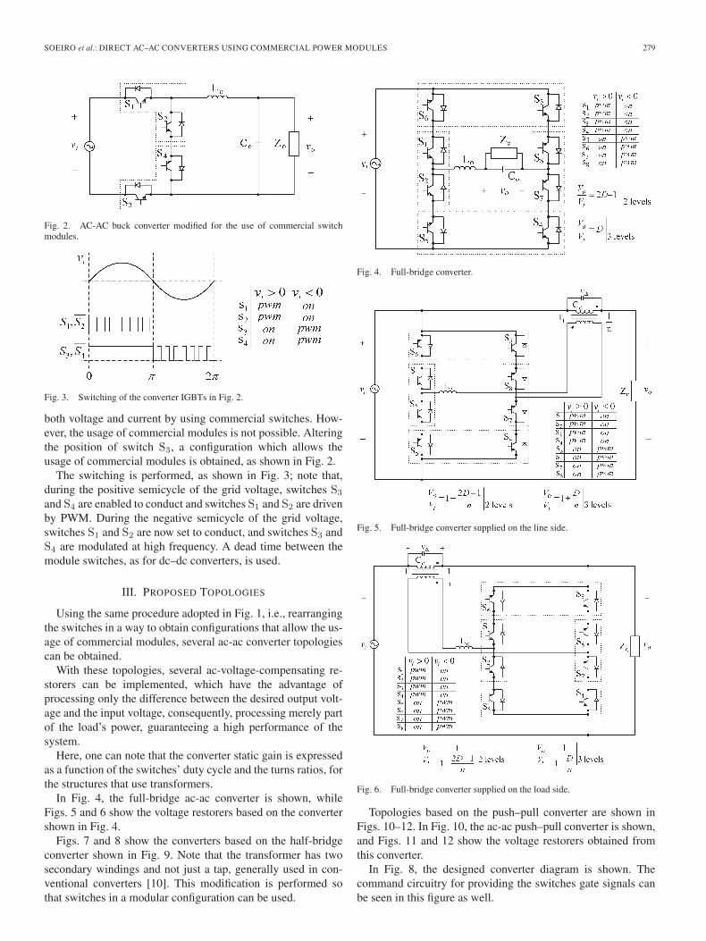
Fig. 2. AC-AC buck converter modified for the use of commercial switchmodules.
Fig. 3. Switching of the converter IGBTs in Fig. 2.
both voltage and current by using commercial switches. How-ever, the usage of commercial modules is not possible. Alteringthe position of switch S3, a configuration which allows theusage of commercial modules is obtained, as shown in Fig. 2.
The switching is performed, as shown in Fig. 3; note that,during the positive semicycle of the grid voltage, switches S3
and S4 are enabled to conduct and switches S1 and S2 are drivenby PWM. During the negative semicycle of the grid voltage,switches S1 and S2 are now set to conduct, and switches S3 andS4 are modulated at high frequency. A dead time between themodule switches, as for dc–dc converters, is used.
III. PROPOSED TOPOLOGIES
Using the same procedure adopted in Fig. 1, i.e., rearrangingthe switches in a way to obtain configurations that allow the us-age of commercial modules, several ac-ac converter topologiescan be obtained.
With these topologies, several ac-voltage-compensating re-storers can be implemented, which have the advantage ofprocessing only the difference between the desired output volt-age and the input voltage, consequently, processing merely partof the load’s power, guaranteeing a high performance of thesystem.
Here, one can note that the converter static gain is expressedas a function of the switches’ duty cycle and the turns ratios, forthe structures that use transformers.
In Fig. 4, the full-bridge ac-ac converter is shown, whileFigs. 5 and 6 show the voltage restorers based on the convertershown in Fig. 4.
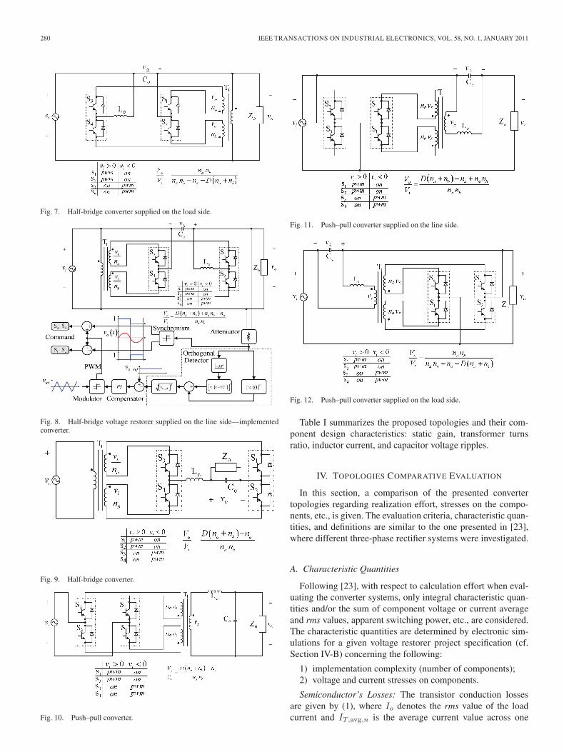
Figs. 7 and 8 show the converters based on the half-bridgeconverter shown in Fig. 9. Note that the transformer has twosecondary windings and not just a tap, generally used in con-ventional converters [10]. This modification is performed sothat switches in a modular configuration can be used.
Fig. 4. Full-bridge converter.
Fig. 5. Full-bridge converter supplied on the line side.
Fig. 6. Full-bridge converter supplied on the load side.
Topologies based on the push–pull converter are shown inFigs. 10–12. In Fig. 10, the ac-ac push–pull converter is shown,and Figs. 11 and 12 show the voltage restorers obtained fromthis converter.
In Fig. 8, the designed converter diagram is shown. Thecommand circuitry for providing the switches gate signals canbe seen in this figure as well.
280 IEEE TRANSACTIONS ON INDUSTRIAL ELECTRONICS, VOL. 58, NO. 1, JANUARY 2011
Fig. 7. Half-bridge converter supplied on the load side.
Fig. 8. Half-bridge voltage restorer supplied on the line side—implementedconverter.
Fig. 9. Half-bridge converter.
Fig. 10. Push–pull converter.
Fig. 11. Push–pull converter supplied on the line side.
Fig. 12. Push–pull converter supplied on the load side.
Table I summarizes the proposed topologies and their com-ponent design characteristics: static gain, transformer turnsratio, inductor current, and capacitor voltage ripples.
IV. TOPOLOGIES COMPARATIVE EVALUATION
In this section, a comparison of the presented convertertopologies regarding realization effort, stresses on the compo-nents, etc., is given. The evaluation criteria, characteristic quan-tities, and definitions are similar to the one presented in [23],where different three-phase rectifier systems were investigated.
A. Characteristic Quantities
Following [23], with respect to calculation effort when eval-uating the converter systems, only integral characteristic quan-tities and/or the sum of component voltage or current averageand rms values, apparent switching power, etc., are considered.The characteristic quantities are determined by electronic sim-ulations for a given voltage restorer project specification (cf.Section IV-B) concerning the following:
1) implementation complexity (number of components);2) voltage and current stresses on components.
Semiconductor’s Losses: The transistor conduction lossesare given by (1), where Io denotes the rms value of the loadcurrent and IT,avg,n is the average current value across one
SOEIRO et al.: DIRECT AC–AC CONVERTERS USING COMMERCIAL POWER MODULES 281
TABLE IVOLTAGE RESTORER DESIGN CHARACTERISTICS
transistor. In a similar way, the diode conduction losses can bedetermined [see (2)].
To obtain the transistor’s switching losses, one utilizes (3).Therein, the turn-on/turn-off losses are determined consideringa constant turn-off voltage UT,off,n, given by the rms value ofthe input or output voltage, depending where the converter issupplied from. In (3), Po represents the system output power,and |iT |avg,n represents the average value of the turn-on/turn-off current across the transistors
PT =1Io
∑n
IT,avg,n (1)
PD =1Io
∑n
ID,avg,n (2)
SP =1Po
∑n
|iT |avg,nUT,off,n. (3)
Rated Power of Inductors and Transformers: The ratedpower of inductive components (inductors and transformers) isevaluated, in such a way that inductors are characterized by therated power of an equivalent transformer [24], [25], as given by(4). For transformers, the rated power transferred is obtained
by (5), where Si denotes the apparent power of a partialwinding [23]
ST,eq =1Po
2.2fNLoILo,rmsILo,max (4)
ST =1Po
∑n
Si. (5)
Capacitor Current Stress: The stress across the capacitor isdetermined by the ratio between its current’s rms values and theoutput current, as shown in
iCo =ICo,rms
Io. (6)
B. Simulation Results
For the sake of brevity, only converters which process merelya part of the load power are analyzed (Figs. 5–8 Fig. 11, andFig. 12). These topologies have higher efficiency and reducedvolume when compared to converters that handle 100% of thesystem power capability (Fig. 2, Fig. 4, Fig. 9, and Fig. 10).
All the analyzed converter topologies were designed accord-ing to the following specifications:
1) vi = 220 V ± 20%/60 Hz; vo = 220 V/60 Hz; So =3 kVA;
2) fs = 20 kHz; ΔiLo = 10%ILo_pk; ΔvCo = 1%Vo_pk.
282 IEEE TRANSACTIONS ON INDUSTRIAL ELECTRONICS, VOL. 58, NO. 1, JANUARY 2011
TABLE II3-kW VOLTAGE RESTORER COMPARATIVE EVALUATION
The transformer turns ratios were defined in such a waythat all systems have similar static gain for a given duty cycleD and maximal-voltage-compensation cases (vi = 220 V ±20%). This allows the voltage restorer topologies to haveequivalent control effort and dynamic behavior in the consid-ered operation points. The load is considered purely resistive.Furthermore, the inductor and capacitors were adjusted to fulfillthe ripple requirements on the maximal-compensation cases.
The simulations performed for determining the characteristiccurrent peak, average, and rms values are based on the follow-ing assumptions:
1) mains’ voltage is purely sinusoidal, with no inner mainsimpedance;
2) ideal components;3) neglection of the switching frequency ripple for the cal-
culation of component peak current values.
The simulation results, including the converter parameters,are compiled in Table II. These results are summarized graph-ically, where the evaluated characteristic (each pentagon axis)high values (in red or bold) are scaled to the maximum obtainedvalue among the analyzed structures. The maximum valuefound is given a mark of ten. Therefore, the converter that hasthe minimum values/area is the most suitable for the considereddesign specification.
Analyzing the results, one can observe that the push–pullconverter fed by the line side presented the best compositionof characteristics, particularly regarding semiconductor losses.On the other hand, the full-bridge three-level topology fed bythe line side presents lower passive component stress character-istics. The drawbacks of the latter topology are the number ofcomponents and, consequently, the implementation complexity.As a consequence, the total cost of the structure increases, whilethe reliability of the system reduces.
The main difference between the push–pull and half-bridgetopologies is in the semiconductor stress characteristics. Dueto the transformer configuration, in the latter one, the currentacross the semiconductor is higher than that for the push–pullconverter, but the block voltage is lower. Therefore, the choicefor one or the other topology is mainly dependent on thecommercially available semiconductor loss characteristics. Itis common that power modules with lower breakdown voltagehave better power loss characteristics. For the specification be-ing considered, the push–pull converter would employ 1200-Vinsulated-gate bipolar transistors (IGBTs), and for the half-bridge voltage restorer, it would use 600-V IGBTs.
It is important to point out that the topologies fed by the loadside have outstanding performance for one region of voltagecompensation (+Δ), which is better than for the same topologyfed by the line side. On the other hand, for the other voltagecompensation region (−Δ), the performance is considerablyworse. However, since the components of the converter have tocope with the maximum stress situation, topologies fed by theload side need higher power rating elements. Therefore, for theconsidered specification, voltage restorers fed by the line sideare less expensive and normally have lower volume than theones fed by the load side (higher power density). Moreover, ascan be observed in the results, this voltage restorer technologyhas more symmetric characteristic behavior for both voltagecompensation regions than the ones fed by the load side.
V. IMPLEMENTED VOLTAGE RESTORER ANALYSIS
AND EXPERIMENTAL RESULTS
A. Converter Design
The voltage restorer which will be implemented in the lab-oratory with the objective of certifying the operation of theproposed topologies is the converter shown in Fig. 8. This
SOEIRO et al.: DIRECT AC–AC CONVERTERS USING COMMERCIAL POWER MODULES 283
is a half-bridge converter which uses a transformer with twosecondary windings and four controlled switches. Lo and Co
comprise the converter’s output filter. Voltage compensation,with proper amplitude and phase, is applied in series withthe input voltage so that the output voltage has the desiredamplitude.
The duty cycle (D) is defined as the ratio between the con-ducting interval of switches S1 and S2 and the total switchingperiod (Ts = 1/fs), considering the positive semicycle of thegrid voltage. During the negative semicycle, the duty cycle isthe ratio between the conducting intervals of switches S3 and S4
and the total time, given by the switching frequency (fs). Theexpressions for the voltage restorer’s static gain, the transformerturns ratios (na and nb), the inductor Lo current ripple, and thecapacitor Co voltage ripple are given in Table I.
Using these expressions, a voltage restorer with the followingparameters was designed:
1) vi = 220 ± 20% V, vo = 220 V, So = 3 kVA;2) fs = 20 kHz, na = 3.2, nb = 4.8, vtri_pkp = 12.6 V;3) Lo = 400 μH, S1 to S4 = IRG4PSC71UD, Co = 10 μF.Fig. 8 shows the simplified circuit of the implemented
voltage restorer. In this figure, note that the output voltageis sampled in order to generate the synchronism signals toproperly obtain the drive signals of the switches, according tothe input/output voltage’s polarity. The control technique usingorthogonal detection is also shown, and the voltage controlleris a classic proportional–integral (PI) [13], [14].
B. Line Impedance Problem
To verify the line impedance Zi(s) effects on the circuitoperation, the mathematical model of the studied topologyis derived considering the ac converter and transformer as acontrolled source which compensates the voltage in series [cf.Fig. 13(a)]. In this model, the line impedance is represented by apure inductance Leq. In (7), shown at the bottom of the page, theoutput-voltage-to-control-voltage transfer function (G(s)) ispresented, and so is the output-voltage-to-input-voltage transferfunction (F (s)) in (8), shown at the bottom of the page. Theaforementioned expressions can be used to study the closed-loop behavior of the converter [cf. Fig. 13(b)].
Analyzing (7), it can be seen that G(s) contains a zeroon the right side of the complex plane. The right-side zeroproblem, which is typical for boost converters in voltage mode,was studied in [26]. This kind of system, often referred toas nonminimum phase, has a unique step input response. Anincremental step in duty cycle implies on an increase in com-pensation voltage vΔ and also on the converter input current.
This current flowing through the line impedance provokes avoltage drop, and so, the output voltage vo initially decreases,during a Δt time interval, rising later as desired to reach steadystate in a stable system [cf. Fig. 14(b)]. In this way, the effectof the positive zero can be interpreted as a delay on the outputvoltage response due to duty cycle variations. Note that, if a fastcontrol loop is used, the changing dynamic of the control signalcan lead the system to instability.
The voltage restorer sensitivity to load Zo variation can beobserved in G(s) and F (s). The system’s dynamic is moreoscillatory and less damped as the load impedance increases.Therefore, in closed-loop operation, the topology can haveinstability problems feeding nonlinear loads such as half-bridgerectifiers, where the current can become discontinuous and haveabrupt variations. In practice, there are parasitic resistances,which lessen the effect of abrupt load variations since theseelements work as dampers to the voltage oscillations.
Electronic simulations are performed to evaluate the effectsof the line impedance on the system dynamic for duty cy-cle variation, and the results are shown in Fig. 14(b). FromFig. 14(b), it can be noticed that the system simulated withoutthe line impedance has no delay and that the output voltage in-creases instantaneously with the increase in d(t). The converterwith the line impedance has delay Δt, and moreover, it has anoutput voltage oscillation due to the voltage drop in Zi(s) fromthe high-frequency circulating current. This voltage oscillationflows through the output voltage sensor, which could causeproblem to the structure’s control. As can be observed, botheffects are attenuated when the input filter shown in Fig. 14(a)is used.
The effects of the positive zero and voltage oscillations canthen be attenuated by using a filter in the converter input todecouple the line impedance from the system [cf. Fig. 14(a)].Another solution is to design a slow control loop, which limitsthe converter’s dynamic response. In the built prototype, thefunction of the input filter is performed by decoupling capac-itors of 10 μF placed on the transformer secondary side.
G(s) =
nan(na+nb)Vo
(D(na+nb)−na+nanb)2 ·
[nanb
D(na+nb)−na+nanb− s
LeqZo
D(na+nb)−na+nanb
nanb
]
s2LeqCo + sLeqZo
+(
nanb
D(na+nb)−na+nanb
)2 (7)
F (s) =nanb
D(na+nb)−na+nanb
s2LeqCo + sLeqZo
+(
nanb
D(na+nb)−na+nanb
)2 (8)
284 IEEE TRANSACTIONS ON INDUSTRIAL ELECTRONICS, VOL. 58, NO. 1, JANUARY 2011
Fig. 14. (a) Converter input filter. (b) Response to a step in duty cycle.
Fig. 15. Orthogonal detector output voltage with sinusoidal and distorted input voltage.
C. Orthogonal Detection Control
The orthogonal detection controller uses trigonometric rela-tions to obtain a continuous voltage value, which is proportionalto the input voltage rms value [13], [14]. If the measured voltageis sinusoidal, then the output of the orthogonal detector willbe proportional to the rms value of the measured voltage (cf.Fig. 8). On the other hand, if the measured voltage is distortedwith harmonics, the output value will not be the actual rmsvalue of this voltage. This problem is shown in Fig. 15, wherethe difference in the output values can be seen, despite thesame rms value of the voltages being applied at the input of theorthogonal detector. This drawback can be lessened if a prefilterstage is employed. Furthermore, this technique could presentoutstanding performance if one combines it with a feedforwardcontrol technique. In this case, the latter one would correct theoutput voltage against disturbances in the input voltage, whilethe orthogonal control would act to correct the rms value of theoutput voltage.
The orthogonal detection control was implemented in aPIC18F252 microcontroller. The converter output voltage issampled (attenuated) and rectified with a precision rectifier,
to then be applied to this microcontroller. The implementedalgorithm determines the rms voltage value according to theprinciple of the orthogonal detection. Therefore, the required90◦ phase shift is carried out by a time delay. At the outputof PIC18F252, there is a practically continuous voltage, whichwill be compared to the reference voltage to generate an errorsignal. This error is compensated by a PI controller, which hasa cutoff frequency of approximately 1.59 kHz, which is morethan 12 times lower than the 20-kHz switching frequency. Notethat, during the start-up, the control algorithm may generatethe wrong control signal vc, and to protect the system, themicrocontroller must limit its value during this process.
D. Experimental Results
In Fig. 16, the drive signals (at low frequency) of switches S1
and S2 are shown, along with the synchronism signal. Note that,during the positive semicycle, these switches are controlled bymeans of a two-level PWM (as shown in details), while duringthe negative semicycle, they conduct continuously. In the samemanner, Fig. 17 shows the drive signals of S3 and S4.
SOEIRO et al.: DIRECT AC–AC CONVERTERS USING COMMERCIAL POWER MODULES 285
Fig. 16. Drive signals of switches S1 and S2.
Fig. 17. Drive signals of switches S3 and S4.
Fig. 18. Voltages across switches S1 and S3.
Fig. 18 shows the voltages across switches S1 and S3 withoutovervoltage, demonstrating the proper operation of the drivestrategy used here. The input and output voltages are shownin Fig. 19; note that, for an input of −10%, the output voltageis being stabilized at 220 V, as desired. Fig. 20 shows the input
and output voltages for a line voltage at 242 V, so the duty cycleis about 0.225.
Observing Figs. 16–20, it can be noticed that the control volt-age is continuous during the whole line voltage period, whichis a characteristic of direct ac-ac converters. As an example,
286 IEEE TRANSACTIONS ON INDUSTRIAL ELECTRONICS, VOL. 58, NO. 1, JANUARY 2011
Fig. 19. Input and output voltages—(vi = 0.9vo, D = 0.613).
Fig. 20. Input and output voltages—(vi = 1.1vo, D = 0.225).
for PWM inverters, the duty cycle varies in a sinusoidal shape,while for indirect ac-ac converters without dc link, varianceoccurs in a rectangular shape [2].
To evaluate the performance of the control technique duringdisturbances, three different tests were conducted: +20% stepchange in the input voltage, +50% step change in the loading,and operation with nonlinear load. These experimental resultsare shown in Fig. 21. Fig. 21(a) shows the results obtainedwith a +20% input voltage step change. As can be noted, theoutput voltage could be corrected to its reference value. For+50% load step, for which the results are shown in Fig. 21(b),one can observe that the system is practically insensitive toload variations. In fact, a small oscillation at the momentthe load is changed can be noted; however, the control canquickly attenuate this disturbance, keeping the stability of thesystem.
The output voltage and the load current for operation witha nonlinear load are shown in Fig. 21(c). As one can observe,the orthogonal detection method does not allow correction ofdistortions in the output voltage, which is mainly caused by thevoltage drop on the line impedance due to the high current peakcirculation.
The prototype implemented in the laboratory is shown inFig. 22. The power stage, drive circuits, control, and command
circuitry can be seen there. Moreover, one can observe thetwo-secondary-winding transformer, the snubber capacitors,the output filter inductor, and capacitors.
VI. CONCLUSION
In this paper, several topologies for direct ac–ac converterspermitting the use of commercial switch modules have beenpresented.
For all the basic converters (buck, full-bridge, half-bridge,and push–pull), we applied the proposed methodology, thusobtaining four converters which have the advantage of usingcommercial switch modules. These converters were used toimplement a voltage restorer that can be supplied either on theline side or on the load side. In this way, eight voltage restorerswere proposed. For all the converters, their characteristics aresummarized in Table I, e.g., the static gain expressions, thetransformer turns ratios, the current, and the voltage rippleacross the converter output filter.
Furthermore, in Table II, a comparative evaluation of thestudied voltage restorer concepts concerning implementationcomplexity and component efforts was presented. From theseconverter topologies, one was chosen for implementation as anexperimental prototype.
SOEIRO et al.: DIRECT AC–AC CONVERTERS USING COMMERCIAL POWER MODULES 287
Fig. 21. Converter operations. (a) +20% step change in the input voltage. (b) +50% step change in the loading. (c) Operation with nonlinear load.
Fig. 22. Picture of the implemented voltage restorer prototype.
The experimental results of the half-bridge prototype areshown, demonstrating the proper operation of the drive strategy,as well as the orthogonal detection control.
The possibility of using commercial modules makes thestudied topologies attractive for high-power applications, eitheras voltage restorers or harmonics, sags, and overvoltage com-pensators, among others.
REFERENCES
[1] H. Kragh, “On the control of a DC-link based high frequency AC-voltageregulator,” in Proc. IEEE PESC, Jun. 2001, pp. 1122–1128.
[2] C. A. Petry, J. C. Fagundes, and I. Barbi, “AC–AC indirect converter forapplication as line conditioner,” in Proc. 7th COBEP, Fortaleza, Brazil,Sep. 2003, pp. 509–514.
[3] P. N. Enjeti and S. Choi, “An approach to realize higher power PWM ACcontroller,” in Proc. APEC, Mar. 1993, pp. 323–327.
[4] E. P. Trabach, P. F. S. Amaral, and D. S. L. Simonetti, “A stabilized singlephase electronic autotransformer,” in Proc. 5th COBEP, Foz do Iguaçú,Brazil, Sep. 1999, pp. 701–706.
[5] B.-H. Kwon, B.-D. Min, and J.-H. Kim, “Novel topologies of AC chop-pers,” Proc. Inst. Elect. Eng.—Electr. Power Appl., vol. 143, no. 4,pp. 323–330, Jul. 1996.
[6] J.-H. Kim, B.-D. Min, B.-H. Kwon, and S.-C. Won, “A PWM buck–boostAC chopper solving the commutation problem,” IEEE Trans. Ind. Elec-tron., vol. 45, no. 5, pp. 832–835, Oct. 1998.
[7] J.-H. Kim and B.-H. Kwon, “Three-phase ideal phase shifter using ACchoppers,” Proc. Inst. Elect. Eng.—Electr. Power Appl., vol. 147, no. 4,pp. 329–335, Jul. 2000.
[8] T. Shinyama, A. Ueda, and A. Torri, “AC chopper using four switches,”in Proc. PCC, Apr. 2002, pp. 1056–1060.
[9] J. C. Fagundes, E. V. Kassick, and I. Barbi, “A PWM AC chopper withoutdead time and clamping circuit,” in Proc. 2nd COBEP, Uberlândia, Brazil,Nov. 1993, pp. 302–307.
[10] C. A. Petry, J. C. Fagundes, and I. Barbi, “High frequency AC regu-lator for non-linear loads,” in Proc. 6th COBEP, Florianópolis, Brazil,Nov. 1999, pp. 491–496.
[11] G. Venkataramanan, “A family of PWM converters for three phase ACpower conditioning,” in Proc. Int. Conf. Power Electron., Drives EnergySyst. Ind. Growth, Jan. 1996, pp. 572–577.
[12] Z. Fedyczak, R. Strzelecki, and G. Benysek, “Single-phase PWM AC/ACsemiconductor transformer topologies and applications,” in Proc. 33rdAnnu. IEEE PESC, Jun. 2002, pp. 1048–1053.
[13] H.-Y. Chu, H.-L. Jou, and C.-L. Huang, “Transient response of a peakvoltage detector for sinusoidal signals,” IEEE Trans. Ind. Electron.,vol. 39, no. 1, pp. 74–79, Feb. 1992.
[14] C.-T. Pan and M.-C. Jiang, “A quick response peak detector for variablefrequency three-phase sinusoidal signals,” IEEE Trans. Ind. Electron.,vol. 41, no. 4, pp. 434–440, Aug. 1994.
[15] E. Meyer, Z. Zhang, and Y.-F. Liu, “An optimal control method for buckconverters using a practical capacitor charge balance technique,” IEEETrans. Power Electron., vol. 23, no. 4, pp. 1802–1812, Jul. 2008.
[16] P. A. Dahono, “A control method for DC–DC converter that has an LCLoutput filter based on new virtual capacitor and resistor concepts,” in Proc.IEEE Power Electron. Spec. Conf., Aachen, Germany, 2004, pp. 36–42.
[17] C. N. Ho, H. S. H. Chung, and K. T. K. Au, “Design and implementationof a fast dynamic control scheme for capacitor-supported dynamic voltagerestorers,” IEEE Trans. Power Electron., vol. 23, no. 1, pp. 237–251,Jan. 2008.
[18] T. Jimichi, H. Fujita, and H. Akagi, “An approach to eliminating DCmagnetic flux from the series transformer of a dynamic voltage restorer,”IEEE Trans. Ind. Appl., vol. 44, no. 3, pp. 809–816, May/Jun. 2008.
[19] L. Garcia de Vicuna, M. Castilla, J. Miret, J. Matas, andJ. M. Guerrero, “Sliding-mode control for a single-phase AC/ACquantum resonant converter,” IEEE Trans. Ind. Electron., vol. 56, no. 9,pp. 3496–3504, Sep. 2009.
[20] C.-H. Liu and Y.-Y. Hsu, “Design of a self-tuning PI controller for a STAT-COM using particle swarm optimization,” IEEE Trans. Ind. Electron.,vol. 57, no. 2, pp. 702–715, Feb. 2010.
[21] R. S. Herrera and P. Salmeron, “Instantaneous reactive power theory: Areference in the nonlinear loads compensation,” IEEE Trans. Ind. Elec-tron., vol. 56, no. 6, pp. 2015–2022, Jun. 2009.
[22] C. A. Petry, J. C. Fagundes, and I. Barbi, “New direct ac–ac convertersusing switching modules solving the commutation problem,” in Proc.IEEE Int. Symp. Ind. Electron., Jul. 9–13, 2006, vol. 2, pp. 864–869.
288 IEEE TRANSACTIONS ON INDUSTRIAL ELECTRONICS, VOL. 58, NO. 1, JANUARY 2011
[23] J. W. Kolar and H. Ertl, “Status of the techniques of three-phase rec-tifier systems with low effects on the mains,” in Proc. 21st INTELEC,Jun. 6–9, 1999, Paper 14–1.
[24] N. Mohan, T. M. Undeland, and W. P. Robbins, Power Electronics—Converters, Applications, Design, 2nd ed. New York: Wiley, 1995.
[25] F. Krismer and J. W. Kolar, “Accurate power loss model derivation of ahigh-current dual active bridge converter for an automotive application,”IEEE Trans. Ind. Electron., vol. 57, no. 3, pp. 881–891, Mar. 2010.
[26] D. M. Sable, B. H. Cho, and B. H. Ridley, “Elimination of the positive zeroin fixed frequency and flyback converters,” in Proc. APEC, Mar. 1990,pp. 205–211.
Thiago B. Soeiro received the B.S. (with honors)and M.S. degrees in electrical engineering from theFederal University of Santa Catarina, Florianópolis,Brazil, in 2004 and 2007, respectively. He is cur-rently working toward the Ph.D. degree in thePower Electronic Systems Laboratory, Swiss Fed-eral Institute of Technology (ETH) Zurich, Zurich,Switzerland.
His research interests include power supplies forelectrostatic precipitator and power factor correctiontechniques.
Clovis A. Petry (M’08) was born in São Miguel doOeste, Santa Catarina, Brazil, in 1972. He receivedthe B.S. degree in electrical engineering and the M.S.and Ph.D. degrees from the Federal University ofSanta Catarina, Florianópolis, Brazil, in 1999, 2001,and 2005, respectively.
He is currently a Professor with the ElectronicsDepartment, Federal Institute for Education, Scienceand Technology of Santa Catarina, Florianópolis. Hisareas of interest are ac–ac converters, line condition-ers, and control of those converters.
João C. dos S. Fagundes was born in Osorio, Brazil,in 1954. He received the B.S. degree in electrical en-gineering from Universidade Federal do Rio Grandedo Sul, Porto Alegre, Brazil, in 1980, the M.Sc.degree in power electronic and drives domain fromthe Federal University of Santa Catarina (UFSC),Florianópolis, Brazil, in 1983, and the Ph.D. degreein electric machines domain from the Institut Na-tional Polytechnique of Toulouse, Toulouse, France,in 1990.
Since 1982, he has been a Professor with theDepartment of Electrical Engineering, UFSC. His fields of interest includepower electronics and drives, high-frequency transformers, and efficient use ofenergy.
Prof. Fagundes is a member of the Brazilian Power Electronics Society(SOBRAEP) and the Brazilian Automation Society (SBA).
Ivo Barbi (M’76–SM’92) was born in Gaspar, SantaCatarina, Brazil, in 1949. He received the B.S.and M.S. degrees in electrical engineering fromthe Federal University of Santa Catarina (UFSC),Florianópolis, Brazil, in 1973 and 1976, respec-tively, and the Dr.Ing. degree from the Institut Na-tional Polytechnique of Toulouse, Toulouse, France,in 1979.
He founded the Brazilian Power Electronics So-ciety and the Institute of Power Electronics (INEP),UFSC. He is currently a Professor with INEP and the
Leader of the power electronics program of UFSC.Dr. Barbi served the IEEE Industrial Electronics Society as an Associate
Editor of the IEEE TRANSACTIONS ON INDUSTRIAL ELECTRONICS, in thepower converters area.