9
•

Loughborough UniversityInstitutional Repository
Direct-write techniques formaskless production of
microelectronics: a reviewof current state-of-the-art
technologies
This item was submitted to Loughborough University's Institutional Repositoryby the/an author.
Citation: ZHANG, Y., LIU, C. and WHALLEY, D.C., 2009. Direct-writetechniques for maskless production of microelectronics: a review of current state-of-the-art technologies. IN: International Conference on Electronic PackagingTechnology & High Density Packaging, (ICEPT-HDP `09), Beijing, China, 10-13 Aug., pp. 497-503
Additional Information:
• This is a conference paper [ c© IEEE]. It is also available from:http://dx.doi.org/10.1109/ICEPT.2009.5270702. Personal use of this ma-terial is permitted. However, permission to reprint/republish this mate-rial for advertising or promotional purposes or for creating new collectiveworks for resale or redistribution to servers or lists, or to reuse any copy-righted component of this work in other works must be obtained from theIEEE.
Metadata Record: https://dspace.lboro.ac.uk/2134/5467
Version: Published
Publisher: c© IEEE
Please cite the published version.

This item was submitted to Loughborough’s Institutional Repository (https://dspace.lboro.ac.uk/) by the author and is made available under the
following Creative Commons Licence conditions.
For the full text of this licence, please go to: http://creativecommons.org/licenses/by-nc-nd/2.5/

2009 International Conference on Electronic Packaging Technology & High Density Packaging (ICEPT-HDP) 978-1-4244-4659-9/09/$25.00 ©2009 IEEE
Direct-write Techniques for Maskless Production of Microelectronics: A Review of Current State-of-the-art Technologies
Yan Zhang, Changqing Liu, and David Whalley
Wolfson School of Mechanical and Manufacturing Engineering, Loughborough University Wolfson School of Mechanical and Manufacturing Engineering, Loughborough University, Loughborough, Leicestershire,
United Kingdom, LE11 3RQ Email: [email protected] Telephone: 44(0)1509 227519
Abstract Recently, there has been growing interest in direct-write
methods for the manufacturing of microelectronic products, as the entire electronics industry sector is aiming towards low cost, rapid manufacturing and shorter time-to-market, as well as reduced environmental impacts. This paper will review the main direct-write techniques, most of which have been invented or seen significant development during the last decade. These techniques include droplet-based direct writing, such as inkjet printing, filament-based direct writing, such as the Micropen and nScrypt processes, tip based direct-write methods, and laser beam direct writing. For each category, only a few examples are presented, although there are a number of specific methods and variants within each of these categories.
Introduction Direct-write technology has many advantages over
traditional, often subtractive, processes where, for example, a film deposition process is followed by subsequent removal of much of this layer.
Figure-1 A traditional subtractive manufacturing process
Figure-1 is a schematic illustration of a conventional
lithographic based subtractive manufacturing process. In this case a conductive layer is first deposited onto the substrate followed by photoresist deposition on top of it. Afterwards masks are used to transfer the required conductor pattern onto the photoresist layer. After development of the photoresist an etching process is used to remove unwanted areas of the conductive layer, leaving the required conductive pattern. As can be seen from the above, traditional manufacturing processes involve a lot of steps, and the temporary application and then removal of all or part of various layers of materials. Such processes therefore create large quantities of material wastes and are also often highly energy consuming such that a 2 gram microchip has been estimated to consume 1.7kg of non-renewable resources [1].
Direct writing is therefore emerging as a potential alternative approach for the manufacturing of microelectronic devices and other micro-engineered components such as MEMS and micro-fluidic devices. Existing lithography techniques also use masks to replicate the CAD created images that define the pattern of each layer, which usually involve additional tooling and manufacturing steps. This will increase the potential for human error and the overall manufacturing cost and time [2, 3]. The subtractive removal of the materials being patterned to form a part of the product, such as a copper conductor layer, and of temporary layers such as photoresist, which do not form a part of the finished product, also generates significant waste and creates environmental problems. Direct-write techniques promise an added value in that they can be incorporated directly with the output from CAD/CAM software to generate circuit patterns, which can be subsequently tailored for digital imaging. It is agile as any changes made within the CAD system, for example to include new design features or necessary modifications, can be immediately implemented without the delays associated with manufacture of revised photo-tools. Therefore, it enables the rapid prototyping of a new product from its initial design, in comparison with the costly and time-consuming mask generation and lithography processes. In addition to being more cost effective, flexible and providing a rapid turn-round, as a data-driven process, direct-write techniques can minimize the usage of materials and potentially reduce energy consumption [4], thereby reducing the large environmental burdens associated with micro-engineered product manufacture. In many direct writing processes, materials can be deposited only where needed and no further etching or removal is necessary. This simplifies the manufacturing process and reduces the requirement for processing and disposal of hazardous and toxic substances. Such data driven processes also provide the possibility of greater customisation of products to specific applications.
Definition and classification Many different variants of a definition of direct writing
have been offered in various papers by different researchers [5-7]. In this paper, direct writing is defined, by combining several of these previous definitions, as additive techniques enabling the deposition of electronic components and functional or structural patterns, out of different kinds of materials, directly following a preset layout in a data driven way without utilizing masks or subsequent etching processes. After material deposition onto the substrate is completed, a further heat treatment process, such as curing or sintering, is often needed in order for the deposited material to achieve its full performance.
497
Authorized licensed use limited to: LOUGHBOROUGH UNIVERSITY. Downloaded on November 11, 2009 at 11:38 from IEEE Xplore. Restrictions apply.

2009 International Conference on Electronic Packaging Technology & High Density Packaging (ICEPT-HDP)
A variety of direct-write methods have been created and developed over recent years. However, no matter what devices are involved for implementation, or whatever the fundamental principle behind each technique is, most of the existing direct-write techniques can be classified into one of these four categories: (1) droplet-based direct writing; (2) filament-based direct writing, which is sometimes referred to as a continuous approach or flow-based technique; (3) tip based direct writing; and (4) laser based direct writing.
Droplet-based direct writing Droplet based direct write methods rely on ejection of
droplets of a liquid material from a single nozzle or multiple nozzles. The main sub-categories of droplet-based methods are those based on ink jet printing and the Aerosol Jet process. For these processes the jetted material must be a liquid at temperatures compatible with the process equipment.
Inkjet printing has demonstrated its remarkable power in areas such as home and office personal computer based printing and is also widely used in industrial and commercial applications, for example in high speed contactless marking of foodstuffs and packaging. The idea of applying inkjet printing to fields such as electronic manufacturing and solid free-form (SFF) fabrication developed during the 1980s [5], but only recently applications in printed electronics, MEMS, wireless communication, etc, have become the driving force behind the adaptation of inkjet printing [5].
There are two key types of inkjet type technologies, continuous jetting and drop on demand (DoD). For DoD systems there are two main types of actuation method; used in commercial inkjet printers, piezoelectric inkjet nozzles and thermal inkjet nozzles.
In a thermal inkjet nozzle, when printing of a dot is required, an electrical pulse is applied to a small ohmic heater in the nozzle, and the generated heat vaporizes a small quantity of the volatile ink so as to form a bubble. When this happens it creates a pressure difference between the interior and exterior of the nozzle, resulting in a droplet being ejected from the orifice and propelled towards the printing substrate. As the heater then cools the bubble collapses and a pressure difference between the interior and exterior of the ink cavity again occurs, but ink is now sucked into the cavity from the reservoir to replace the jetted material and restore the pressure balance.
In a piezo-type inkjet head, the actuation method relies on deformation of a piezo-electric material to create the pressure to eject a droplet from the nozzle. Piezo-electric materials are capable of transforming external mechanical inputs into electrical outputs and vice versa. So when a changing electrical voltage is applied to the piezo-material, it deforms in response to the signal input. If the voltage waveform applied to the piezo-material is transient, a deformation pulse corresponding to the voltage pulse should be expected. Material expansion due to this voltage propels an ink droplet from the orifice and ink is then drawn from the reservoir to refill the cavity in compensation for the pressure discrepancy when the voltage drop disappears and the piezo material returns to its previous steady state dimensions. The maximum temperature at which a material may be jetted is
limited by the piezo-electric material, which will cease to function above some temperature threshold.
In a continuous mode inkjet system, a transducer typically made from piezoelectric material is used to generate pressure waves within a pressurised ink reservoir in response to the continuous application of an alternating current. As the transducer may be remote from the reservoir, continuous mode jetting does not have the same temperature limits as DoD jetting. Pressurisation of the reservoir ensures a continuous stream of the material being jetted passes through the nozzle and issues from the orifice, where it breaks up into individual uniform droplets in response to the waveform. The droplet stream subsequently passes through an electrostatic charging field to acquire an electrostatic charge so that use of a deflection field allows the droplet stream to be directed onto the required locations on the substrate. Those not deflected by the deflection field are collected into a gutter and may be recycled for later reuse.
Both types of system are available from a range of vendors as either a print head or a full printing system. There are several print-head assemblies to choose from depending on the specific application requirements. The nozzle orifice diameter controls the droplet volume and therefore feature resolution that can be achieved. The resolution also depends on several other factors such as wettability of the ‘‘ink’’ onto the substrate, ink curing speed, and so on. Microfab has successfully demonstrated its piezo based printing platforms’ abilities in solder bumping, embedded passives, and for printing of other material types such as dielectric materials and adhesives, components of fuel cells, organic light-emitting diodes, waveguides, micro lenses and so on. Figure-2 is an illustration of a flip-chip with a perimeter array of jetted solder bumps with 60μm balls on 150μm centres. For continuous systems droplet sizes range from 20μm to 1mm, with 150μm being the typical feature size. For DoD systems, the achievable droplet diameter ranges from 15μm to 100μm [8].
Figure-2 Jetted flip-chip solder bump [9]
Aerosol Jet is a registered trademark of Optomec®. The
Aerosol Jet system is mainly composed of two key components, the atomizer and the deposition head, marked as ① and ② in Figure-3 respectively. The raw material to be deposited must be in a liquid form and is first placed into an either ultrasonic or pneumatic atomizer, which is utilized to generate a dense vapour of material droplets between 1-5 microns in size - a process known as ‘mist generation’. Then the generated mist, or aerosol, is transferred into a tightly
498
Authorized licensed use limited to: LOUGHBOROUGH UNIVERSITY. Downloaded on November 11, 2009 at 11:38 from IEEE Xplore. Restrictions apply.

2009 International Conference on Electronic Packaging Technology & High Density Packaging (ICEPT-HDP)
confined jet, within what is known as the deposition head, by a gas flow running through the atomizer and out into the deposition head. The aerosol stream brought into the deposition head is further focused by a second gas flow introduced into the jet. The aerosol stream and the newly introduced sheath gas flow interact with each other and form a co-axial annular flow, which then leaves the deposition head through a nozzle attached to it and lands on the substrate. Optomec® offers a laser module that can be integrated into the system to locally complete thermal post-processing of the deposited material, e.g. by sintering of a nano or micro particles, and for some materials such as gold and silver has been shown to achieve properties as good as the bulk materials, but without damaging substrates which have low heat endurance capability. The printing process of the Aerosol Jet system provides a non-contact way of printing, like inkjet printing, which makes it compatible with processes where contamination of the substrate must be avoided.
Figure-3 Illustration of the Optomec® Aerosol Jet
operating principle
The Aerosol Jet system can create lines as fine as 10 microns with a minimum pitch of 20 microns, or as wide as 150 microns. The material handling ability in terms of viscosity falls into a wide range, i.e. between 0.001 and 2.5 Pascal second (Pa·s), which enables deposition of a wide range of materials [10].
Figure-4 An example of silver lines written using the
Aerosol Jet system over a trench [10]
Figure-4 shows an example of silver lines written over a trench using Aerosol Jet printing, where the line width is 60μm and the trench depth is 500μm. Aerosol Jet printing is particularly suited to such 3D applications as its deposition head can be tilted at an angle to follow the contour of the substrate without contact. Compared with traditional inkjet
printing, Aerosol Jet has the following advantages: its stand-off distance can be adjustable between 1mm to 5mm instead of being fixed as in an inkjet printing system; and the aerosol is a continuous stream composed of high density micro-droplets which are tightly focused resulting in a fine feature definition ability and the nozzle is also more clog resistant [11].
Filament based direct writing Filament based direct writing (FBDW) also requires a
liquid material for dispensing, but differs from the inkjet direct writing processes in that the material flows continuously instead of being jetted as droplets and the material viscosity may therefore vary over a much greater range. Two commercially available examples of this process are discussed here: MicroPen and nScrypt.
The working principle of MicroPen writing can be described as follows:
Material to be deposited is first loaded into a syringe, which is connected with the writing head, referred to as a “block” by the system vendor. The material is squeezed out of the syringe into the writing head by compressing the plunger of the syringe using a pneumatic ram. The material transferred into the “block” is then pressurized up to almost 14MPa (2,000 psi), from where it flows into a micro-capillary writing tip, which deposits the material onto the substrate. A schematic configuration of the MicroPen writing system is presented in Figure-5.
Figure-5 Schematic of the MicroPen system [12]
MicroPen direct writing can deposit potentially any liquid
material ranging in viscosity from 0.005 to 500 Pa·s, which is quite a large range. MicroPen not only deals with a wide range of materials, but also possesses the capability of depositing materials onto a range of substrates, including flexible and non-planar substrates. The MicroPen technique is also a non-contact technology, with the micro-capillary writing tip not touching the surface.
Another filament based direct writing technique is the nScrypt dispensing technique, where a direct-print dispensing tool is integrated with nScrypt’s novel pump called Smart Pump TM, which is illustrated in Figure-6.
The integrated smart pump is able to dispense materials with a viscosity of up to 1,000 Pa·s with accurately controlled air pressure, valve opening and dispensing height [13]. When dispensing is initiated, a valve opens so as to allow the material to be dispensed to flow through the dispensing tip onto the substrate. Once dispensing stops, the valve closes to block material from leaking. One advantage of the smart pump is that it includes a sucking-back
499
Authorized licensed use limited to: LOUGHBOROUGH UNIVERSITY. Downloaded on November 11, 2009 at 11:38 from IEEE Xplore. Restrictions apply.

2009 International Conference on Electronic Packaging Technology & High Density Packaging (ICEPT-HDP)
movement of materials into the dispensing nozzle when deposition is terminated. A negative pressure is maintained in the dispensing tip chamber to induce material sucking back when deposition is ceased. This feature allows the orifice to be left clean and clear without -any agglomeration of- material or the possibility of nozzle clogging, and delivers a consistent start every time dispensing commences. Consequently line printing can be precisely controlled and the width of the dispensed material can be maintained consistent without bulges at the ends.
Figure-6 The nScrypt Smart Pump TM [13]
Tip based direct writing The dip-pen nanolithography (DPN) technique utilizes an
atomic force microscope (AFM) tip to deliver molecules from the dispensing AFM tip onto substrates, which is especially useful in nanoscale applications.
Piner, et al, discovered this technique while investigating a problem that had baffled researchers in atomic force microscopy for a long time that condensed water can either be transported from the substrate to the AFM tip or vice versa depending on the relative humidity and substrate wetting properties [14]. Due to the capillary effect, the AFM tip is capable of dispensing ink adhering to it, from previous dipping, onto substrates which have an affinity for the ink, in a similar way to a dip pen writing on a piece of paper, as shown in Figure-7.
With traditional AFM cantilever tips, dip-pen nanolithography can create features as fine as 12nm in line width and 5nm in spatial resolution. This resolution can be further improved by using sharper cantilevers, but the finest resolution that this process can achieve is still uncertain [5].
Thermal dip pen nanolithography (tDPN) is a modified version of dip pen nanolithography utilising an atomic force microscopy tip which is compatible with heat. The pen tip is first coated with the material to be dispensed in a solid form. When heated, the coated material on the pen tip will melt due to heat transfer and will flow over the pen tip surface onto the substrate. It is claimed that using meltable inks has many advantages. Writing can be switched on and off readily and the ink flow rate can be varied easily by controlling the tip
temperature. Complex 3D structures can be generated through writing layer by layer with the previously deposited layer being solid. And it is compatible with other traditional semiconductor manufacturing methods, since thermal dip pen nanolithography can be performed in vacuum [15].
Figure-7 Schematic illustration of DPN [14]
The finest feature researchers have achieved with tDPN is
close to 75 nm wide. Researchers has also successfully demonstrated writing indium metal onto a substrate and the potential operating temperature is claimed to be much higher than the melting point of indium, as high as 1000°C. One key feature of tDPN lies in that it enables ink to be deposited with such abundant thermal energy as to organize into monolayers prior to its solidification [15].
Polymer pen lithography is a high-throughput and low-cost tip based direct writing method, which is another variant of dip pen nanolithography. It does not use an actual AFM tip to dispense materials, but utilizes polymer tips instead. Its high-throughput feature compensates for DNP’s weakness at the micro scale, which makes it a very promising method for large scale manufacturing. Thousands of, or even millions of, polymer pens can be made together into a polymer pen array which by dispensing materials onto the substrate simultaneously could rapidly create much larger features than individual pens [16]. When the tips of the polymer pen array contact the substrate, their ink coating can be delivered onto substrate.
Laser based direct writing Laser based direct writing techniques rely on using a laser
to process materials so that they can be deposited onto a substrate. The popularity of lasers in direct writing results mainly from a subtractive process called laser micro-machining, however there are many other types of laser based methods such as laser chemical vapour deposition (LCVD) [17], electro-less plating or electroplating with laser assistance [18,19], matrix assisted pulsed laser evaporation direct write (MAPLE-DW) [20], etc.. Some laser based patterning methods are subtractive methods, but are still sometimes considered direct writing, however this paper only introduces additive methods of depositing materials, in line with definition given at the beginning as their being an additive technique without etching.
500
Authorized licensed use limited to: LOUGHBOROUGH UNIVERSITY. Downloaded on November 11, 2009 at 11:38 from IEEE Xplore. Restrictions apply.

2009 International Conference on Electronic Packaging Technology & High Density Packaging (ICEPT-HDP)
Figure-8 Schematic of a (a) laser-guided direct-write
(LGDW) system and (b) flow-guided direct write (FGDW) system [5]
Figure-8 a and b illustrate flow-guided and laser-guided
direct writing techniques respectively. In these techniques a liquid precursor or colloid suspension is first transformed into an aerosol usually by ultrasonic atomization devices or pneumatic nebulisation depending on the particle size of the starting liquid precursor or colloid suspension, just like the mist generation in the Aerosol Jet system. This dense aerosol is then introduced into the deposition devices and focused by the optical and hydrodynamic forces occurring due to momentum transfer between the laser beam and aerosol particles into a narrow beam. For the laser-guided direct-write system, the laser and the generated mist are both transmitted through a hollow optical fibre to guide the particles towards the substrate. The deposition rate ranges from 1 to 10,000 particles per second. But for flow guided direct write, the deposition rate can be higher than 10,000 particles per second, and particle velocity can increase from 1m/s to 10m/s. The accuracies for LGDW and FGDW are 2μm and 25μm respectively [5]. In flow guided direct write, a sealed chamber is fed with the generated aerosol by a gas flow and these particles come out of an orifice with diameter of one millimetre. The particles are then joined by a second gas flow which forms a cylindrical sheath to protect the mist. These combined streams then pass through another small hole to be further focused again and deposited onto the substrate with the assistance of the laser beam.
Laser induced forward transfer (LIFT) is another laser based direct write technique. The general principle is illustrated in Figure-9. The material to be written is first
deposited on a laser-transparent support as a thin film. The support with the thin film on it is brought close to the substrate. The laser is focussed at the interface between the transparent support and the thin film layer where it induces some of the target material to vaporise and propel the rest of the thickness of the material onto the receiving substrate.
Figure-9 Laser induced forward transfer scheme [21]
Conclusions In this paper, each of the main types of direct writing
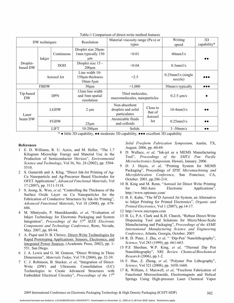
technique were discussed and examples presented. The focus has been on the basic principles of those methods, together with some examples of applications. Table-1[5, 10, 14-16, 22] compares the main features of some of the methods discussed above. For some of these processes the deposition rate quoted is volumetric whilst for other it is a linear deposition rate.
Even though direct-write processes are beginning to demonstrate their potential impact on future microelectronic manufacturing, there are still some significant technical barriers and challenges to be overcome before any further breakthrough can be achieved in terms of widespread industrial application. For instance, in inkjet printing processes, not only the ink formulation poses a great challenge, in terms of rheological properties, particle suspension, wetting and adhesion behaviour, etc. [23,24], but also the interactions of the ink with the substrates are critical in determining the stability, integrity and resolution of such ink-jetted micro sized structures. Since features to be deposited are tailored with the functionality of the materials formulated in ink, it is vitally important to consider the evolution of the materials during processing. Furthermore, full integration through creation of multilayered structures or full 3D approaches require precise positioning and alignment accuracy, and the achievable feature resolution also demands some further developments in the fundamental understanding of these processes.
501
Authorized licensed use limited to: LOUGHBOROUGH UNIVERSITY. Downloaded on November 11, 2009 at 11:38 from IEEE Xplore. Restrictions apply.
2009 International Conference on Electronic Packaging Technology & High Density Packaging (ICEPT-HDP)
Table-1 Comparison of direct-write method features
DW techniques Resolution Material viscosity range (Pa·s) or types
Writing speed
3D capability*
Droplet-based DW
Inkjet Continuous
Droplet size 20μm-1mm typically 150
μm <0.01 60mm3/s
●●
DOD Droplet size 15 -200μm <0.04 0.3mm3/s
Aerosol Jet Line width 10-
150μm thickness 10nm-5μm
<2.5 0.25mm3/s (single nozzle) ●●●
FBDW 50μm <1,000 50mm/s typically ●●●
Tip-based DW DPN
12nm line width and 5nm spatial
resolution
Thiol molecules, macromolecules, nanoparticles 0.2-5 μm/s ●
Laser beam DW
LGDW 2 μm Non-absorbent
droplets and solid particulates
Close to that of
Aerosol Jet
10-4mm3/s ●●
FGDW 25μm
Atomizable fluids and colloids 0.25mm3/s ●●
LIFT 10-200μm Solids 3 -50mm/s ●● * ● little 3D capability, ●● moderate 3D capability, ●●● excellent 3D capability
References 1 E. D. Williams, R. U. Ayres, and M. Heller, “The 1.7
Kilogram Microchip: Energy and Material Use in the Production of Semiconductor Devices”, Environmental Science and Technology, Vol 36, No. 24 (2002), pp. 5504-5510.
2 S. Gamerith and A. Klug, “Direct Ink-Jet Printing of Ag-Cu Nanoparticle and Ag-Precursor Based Electrodes for OFET Applications”, Advanced Functional Materials, Vol 17 (2007), pp. 3111-3118.
3 S. Jeong, K. Woo, et al, “Controlling the Thickness of the Surface Oxide Layer on Cu Nanoparticles for the Fabrication of Conductive Structures by Ink-Jet Printing”, Advanced Functional Materials, Vol 18 (2008), pp. 679-686.
4 M. Mäntysalo, P. Mansikkamäki, et al, “Evaluation of Inkjet Technology for Electronic Packaging and System Integration”, Proceedings of the 57th IEEE Electronic Components and Technology Conference, Reno, Nevada, May. 2007, pp. 89-94.
5 A. Piqué and D. B. Chrisey, Direct-Write Technologies for Rapid Prototyping Applications: Sensors, Electronics, and integrated Power Sources, (Academic Press, 2002), pp. 1-551. San Diego.
6 J. A. Lewis and G. M. Gratson, “Direct Writing in Three Dimensions”, Materials Today, Vol 7/8 (2004), pp. 32-39.
7 C. J. Robinson, B. Stucker, et al, “Integration of Direct-Write (DW) and Ultrasonic Consolidation (UC) Technologies to Create Advanced Structures with Embedded Electrical Circuitry”, Proceedings of the 17th
Solid Freeform Fabrication Symposium, Austin, TX, August. 2006, pp. 60-69.
8 D. Wallace, et al, “Ink-jet as a MEMS Manufacturing Tool”, Proceedings of the SMTA Pan Pacific Microelectronics Symposium, Hawaii, January. 2006.
9 D. J. Hayes, et al, “Printing System for MEMS Packaging”, Proceedings of SPIE Micromachining and Microfabrication Conference, San Francisco, CA, October. 2001, pp.206-214.
10 B. King and M. Renn, “Aerosol Jet Direct Write Printing for Mil-Aero Electronic Applications”, http://www.optomec.com/
11 B. E. Kahn, “The M3D Aerosol Jet System, an Alternative to Inkjet Printing for Printed Electronics”, Organic and Printed Electronics, Vol 1 (2007), pp.14-17.
12 http://www.micropen.com 13 B. Li, P.A. Clark and K.H. Church, “Robust Direct-Write
Dispensing Tool and Solutions for Micro/Meso-Scale Manufacturing and Packaging”, Proceedings of the ASME International Manufacturing Science and Engineering Conference, Atlanta, Georgia, October. 2007.
14 R. D. Piner, J. Zhu, et al, “ ‘Dip-Pen’ Nanolithography”, Science, Vol 283 (1999), pp. 661-663.
15 P.E Sheehan, W.P. King, et al, “Thermal Dip Pen Nanolithography”, NRL Review Chemical/Biochemical Research (2006), pp.1-2.
16 F. Huo, Z. Zheng, et al, “Polymer Pen Lithography”, Science, Vol 321 (2008), pp. 1658-1660.
17 K. William, J. Maxwell, et al, “Freeform Fabrication of Functional Microsolenoids, Electromagnets and Helical Springs Using High-pressure Laser Chemical Vapor
502
Authorized licensed use limited to: LOUGHBOROUGH UNIVERSITY. Downloaded on November 11, 2009 at 11:38 from IEEE Xplore. Restrictions apply.

2009 International Conference on Electronic Packaging Technology & High Density Packaging (ICEPT-HDP)
Deposition”, Proceedings of the 12th IEEE International Conference on Micro Electro Mechanical Systems, Orlando, Florida, January. 1999 pp. 232-237.
18 R.J. Von Gutfeld, et al, “Laser-Enhanced Plating and Etching: Mechanisms and Applications”, IBM Journal of Research and Development, Vol 26 (1982), pp. 136-144.
19 R.J. Von Gutfeld, et al, “Laser Enhanced Electroplating and Maskless Pattern Generation”, Applied Physics Letters, Vol 35 (1979), pp. 651-653.
20 A. Pique, et al, “A novel Laser Transfer Process for Direct Writing of Electronic and Sensor Materials”, Applied Physics A, Vol 69 (1999), pp. S279-S284.
21 M. Colina, P. Serra, et al, “DNA Deposition through Laser Induced Forward Transfer”, Biosensors and Bioelectronics, Vol 20 (2005), pp.1638-1642.
22 K.K.B. Hon, et al, “Direct Writing Technology – Advances and Developments”, Manufacturing Technology, Vol 57 (2008), pp.601-620.
23 D. Kim, S. Heong, et al, “Direct Writing of Silver Conductive Patterns: Improvement of Film Morphology and Conductance by Controlling Solvent Compositions” , Applied Physics Letters, Vol 89 (2006), pp. 264101-1~264101-3.
24 I. Shim, Y. Lee, et al, “An Organometallic Route to Highly Monodispersed Silver Nanoparticles and Their Application to Ink-Jet Printing”, Materials Chemistry and Physics, Vol 110 (2008), pp. 316-321.
503
Authorized licensed use limited to: LOUGHBOROUGH UNIVERSITY. Downloaded on November 11, 2009 at 11:38 from IEEE Xplore. Restrictions apply.


![Database Recovery Techniques - Wikispacesbcompsc1107.wikispaces.com/file/view/2360_Elmasri_6e_Ch23.pdf · Write a [checkpoint] ... Database Recovery Deferred Update with concurrent](https://static.documents.pub/doc/80x56/5af644ae7f8b9a190c8f76ef/database-recovery-techniques-w-a-checkpoint-database-recovery-deferred-update.jpg)


