230
Welcome to ISMT / SRC Maskless Lithography Workshop Chairmen: Dan Herr / Semiconductor Research Corp Scott Mackay / International SEMATECH

Welcome to ISMT / SRCMaskless Lithography
WorkshopChairmen:Dan Herr / Semiconductor Research CorpScott Mackay / International SEMATECH

RSM Maskless Litho Workshop Opening remarks 8/28/01 2
Information & Welcome• Administration / Information / Facilities
• What is Maskless Lithography?
• Agenda
• What should we expect to accomplish today?
• Timing and Requirements for technology introduction
• Your job today...

RSM Maskless Litho Workshop Opening remarks 8/28/01 3
Open Conference Confidentiality Notice• This meeting is an OPEN CONFERENCE.
• Confidential or Proprietary information may NOT be disclosed.
• All meeting attendees are permitted to take notes or otherwise make a personal record of these proceedings.
• All presentations will be available to the public via the International SEMATECH public website following this meeting.

RSM Maskless Litho Workshop Opening remarks 8/28/01 4
Registration TableOpen Tuesday 0700
SALON II & III General SessionTuesday 8/28
SALON ILunch
Tuesday 8/28
EXITS
Meeting Room Floor Plan

RSM Maskless Litho Workshop Opening remarks 8/28/01 10
Breakout Session Locations
• Breakout session locations
– Green & Red in general meeting room
– Yellow in Consulate Room
– Blue in Ambassador Room

RSM Maskless Litho Workshop Opening remarks 8/28/01 5
ML2 Workshop Meeting Groundrules
• What will be discussed– Questions/answers about ML2 technical challenges,
risks, and readiness
• What will NOT be discussed– Politics– Program management– Confidential plans or technology– Business issues (funding, intellectual property, etc.)

RSM Maskless Litho Workshop Opening remarks 8/28/01 6
What is Maskless Lithography?
• Beginning assumptions about “MaskLess Lithography”
– No mask - data fed straight through from tape to tool– Large data transfer rates (multi-tips and/or high
transfer rate) ~10 Tbits/sec– High throughput tools, ~20 WPH– Tool costs below competitive lithography strategies– Potential solution to:
• Rising mask costs• Short-run and development activities in IC companies

RSM Maskless Litho Workshop Opening remarks 8/28/01 7
Why Maskless Lithography?
• CoO models suggest that for small runner parts, ML2 may be most cost effective method of Mfg
• Recent calculations suggest for 50nm node, TP=5 WPH has better CoO that other NGL <3000 wafers/mask!
IST Dec. '99 50nm NGL CoO Analysis (With 'Pellicle-less Tax')
$0
$50
$100
$150
$200
$250
0 1000 2000 3000 4000 5000 6000 7000 8000Mask Usage (wfr/mask)
CoO
($/G
WLE
)
EUV
1X X-Ray
Scalpel
IPL
MEBDW
RSM Maskless Litho Workshop Opening remarks 8/28/01 8
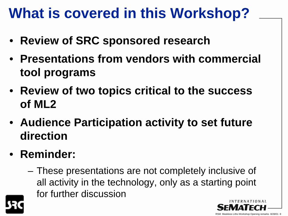
What is covered in this Workshop?
• Review of SRC sponsored research• Presentations from vendors with commercial
tool programs• Review of two topics critical to the success
of ML2• Audience Participation activity to set future
direction• Reminder:
– These presentations are not completely inclusive of all activity in the technology, only as a starting point for further discussion

RSM Maskless Litho Workshop Opening remarks 8/28/01 9
Agenda0800 Welcome / Introduction S. Mackay
0830 Review SRC Activities D. Herr0930 BREAK0945 ETEC M. Gesley1030 Canon N. Deguchi1115 Micronic J. Freyer1200 LUNCH1300 Emission Systems, LLC H. Lockwood1345 Source development D. Lowndes1430 Review of Data Path / Volume Issues K. Standiford1515 BREAK1530 Breakout Sessions : Identify Critical Issues / Review Industry Impact 1630 Review Results / Wrap-up1700 ADJOURN

RSM Maskless Litho Workshop Opening remarks 8/28/01 11
What should we expect to accomplish?
• Purpose:– Review Progress in Maskless Lithography activities– Evaluate where industry can impact the progress of
the programs
• Expected outcome:– Audience has a better understanding of the
maskless lithography technology status – Vision as to when maskless lithography could make
an impact to the ITRS (node and timing)– Identification of critical issues that need to be
demonstrated

RSM Maskless Litho Workshop Opening remarks 8/28/01 12
95 97 99 01 05 07 10
1994 SIA
1997 SIA
1998 / 1999 ITRS
Min
imum
Fea
ture
Siz
e (n
m)
(DR
AM
Hal
f-Pitc
h)
500
350
250
180
130
100
70
50
35
2595 97 99 01 05 07 10
ISMT Litho 2001 Plan(2-year cycle to 50nm)
ITRS Roadmap Potential Acceleration
2000/2001 ITRS
03
03
Proposed ML2
Introduction

RSM Maskless Litho Workshop Opening remarks 8/28/01 13
Timing and Requirements
• Survey of ISMT and SRC member companies– Focused on how the technology would be used
• e.g., development (product/device/process) or production
– Requirements for technology (tool) capability• Throughput / CoO• Wafer size / field (Die) size• Process compatibility
– Timing– Progress on Critical Issues– Potential Research / development area

RSM Maskless Litho Workshop Opening remarks 8/28/01 14
Survey Results…..
• ML2 could be used for:– Product / device development if:
• Available for N+1 to N+3 nodes• Available now to early ‘03• 300mm capable and compatible with DUV processing
– Production (possibly only for critical levels) -• Maintain throughput to tool cost ratio (CoO)• Available for~35nm node• Available in ‘04-’06

RSM Maskless Litho Workshop Opening remarks 8/28/01 15
• Issues that still need to be resolved are:– Data handling for high data volumes– CD error sources in direct-write– Need to demonstrate high throughput approaches– Demonstration of parallel illumination sources– Solution for market acceptance
Survey Results…..

RSM Maskless Litho Workshop Opening remarks 8/28/01 16
Your Job Today...
• Listen critically!– Are the programs tracking the needs of the industry?– Are the program timing and requirements meeting
your expectations?
• Develop opinions
• Constructively feedback in afternoon sessions
– Provide feedback on technology progress– Provide areas of further work (Critical Issues) that
need to be addressed

A Brief Overview of SRC/DARPA’sUniversity Research Initiative in
Maskless Lithography
Maskless Lithography WorkshopPasedena, CA
August 28, 2001
Daniel HerrSemiconductor Research Corporation
Research Triangle Park, NCWith contributions from:
H. Levinson and colleagues fromthe SRC/DARPA Lithography Network

Overview Trends
Status
Opportunities and Challenges
SRC/DARPA Research Vectors
Summary

Lithography Exposure Tool Potential Solutions
Proposed 2001 ITRS Update - Work-in-Progress - Not for Publication
2007 20102001 2013 2016First Year of IC Production 2004
Tec
hn
olo
gy
Op
tio
ns
at T
ech
no
log
y N
od
es (
DR
AM
Hal
f P
itch
, nm
248 nm + PSM193 nm157 nm
193nm + PSM157nmIPL, PEL, PXL
157 nmEUV, EPLML2IPL, PEL, PXL
NarrowOptions
EUVEPLML2IPL, PEL, PXL
EUV, EPLML2Innovative technologyIPL, PEL, XPL
NarrowOptions
NarrowOptions
130
90
65
45
32
22
DRAM Half Pitch(Dense Lines)
NarrowOptions
EUVEPLML2IPL, PEL, PXL

ITRS Roadmap Acceleration95 97 99
1994
1997
1998 & 1999
Min
imu
m F
eatu
re S
ize
(nm
)
500
350
250
180
130
100
70
50
35
2595 97 99 02 05 08 11 14
02 05 08 11 14
Proposed 2000 ITRS Update - 7/21/00, With Proposed Two Year Cycle ( )
Half Pitch(IRC Proposals 7/11/00)
(post-etch)(IRC Proposals 7/11/00)
MPU Gate Length(printed in resist)

EUV is expected to be the NGL lithography ofchoice for 32 nm and 22 nm volume manufacturing.
EUV issues include:
• Need efficient, low debris-producing EUV light sources.*
• Need for high sensitivity resists*; What is the shot noise limit?
• Measure focus errors, when the focus budget is +/- 100 nm?
• How do we measure lens aberrations in-situ?*
• Methods for identifying and mitigating contaminants on EUV
mirrors in situ are needed.
• @λ mask defect inspection needs further development.*
• How can we make an EUV phase-shifting mask?*
• Mask Blanks*• * Research supported by SRC/DARPA Harry LevinsonSummer Study 2001

$100M litho toolsin ~3 generations
1
10
100
Cos
t of
lith
ogra
phy
tool
($M
)
Ix
i-line
248nm
nextgeneration
193nm
Barriers Ahead to Current Roadmap:Cost/Performance Slowdown
LITHOGRAPHY IMPROVEMENTS
Courtesy of K. Brown [NIST]

$0
$5,000,000
$10,000,000
$15,000,000
$20,000,000
$25,000,000
$30,000,000
1980 1985 1990 1995 2000 2005
Year
Exp
osur
e to
ol p
rice Short wavelength
tool prices
Historical tool prices
Exposure tool prices over time
Harry LevinsonSummer Study 2001

Common NGL Issue - Mask CostEstimated Critical Level Mask Prices
0
40
80
120
160
200
Bin
ary
Att
PS
M
Alt
PS
M
Str
ong
OP
C
157n
m
SC
ALP
EL
EU
V
IPL
$K/L
evel
Year 1Year 2Year 3
Source: Brian Grenon, Grenon Consulting Inc.WGO SRC Summer Study 2001
100 NM Node
$1.8M Mask Set, assuming 8 critical EUV layers, @ $165K/layer, and 16 noncritical layers, @ $30K/layer

Projected Mask Prices: 50 NM Node1st vs. 3rd Year in Production
(50nm node)
Mas
k P
rice
($)
0
50000
100000
150000
200000
250000
300000
350000
400000
450000
157n
m+A
TTPSM+OPC (p
ellicl
e)
157n
m+A
TTPSM+OPC (n
o pell
icle)
157n
m+A
LTPSM+OPC (p
ellicl
e)
157n
m+A
LTPSM+OPC (n
o pell
icle)
SCALPEL+EBPC
SCALPEL+EBPC+O
PCEUV (N
o RET)
IPL (N
o RET)
1st Year
3rd Year
(50nm node)
Courtesy of G. Gross
$2.5M Mask Set, assuming 8 critical EUV layers, at$250K/layer, and 16 noncritical layers, @ $30K/Layer

Mask vendors deny high costDespite all the wailing about $1M mask sets looming in the future,Photronics Senior VP Steve Carlson noted that prices for averagereticles have actually increased at a slower rate than theconsumer price index, or a stereo set. - or pork bellies. In fact,only advanced masks have reached parity with pork bellies, whilethe average price actually lags the pork belly price. And I think thattechnology is mature,” Carlson noted at Semicon West. Whileprices of advanced masks increased at a CAGR of 14% over thelast 10 years, the price of low-end masks actually declined.
But new technology leadsto $1,000,000 pork bellies

So, Why do users want maskless lithography?
Source: Ed Muzio, International Sematech
Projected Annual Mask Costs:
ASIC Companies:
~$600 M/yr 100 nm nodea
~$900 M/yr 50 nm nodea
a at one design test per day
IC Manufacturers:
~$ 90 M/yr 100 nm nodeb
~$130 M/yr 50 nm nodeb
b at one mask set per week
Production Impact ~ $10/chip

“Direct-Write” Maskless Lithography
What is maskless lithography?Pattern generation on the wafer
How?Typically viewed as e-beam turf: “EBDW”Many proposals for multi-e-beam wafer
writers as well as cell projectionBut there are many other possibilities - the
key is massively parallel arrays of writersWhen?
Minimum of 5-7 years to beta tool
WGO SRC Summer Study 2001
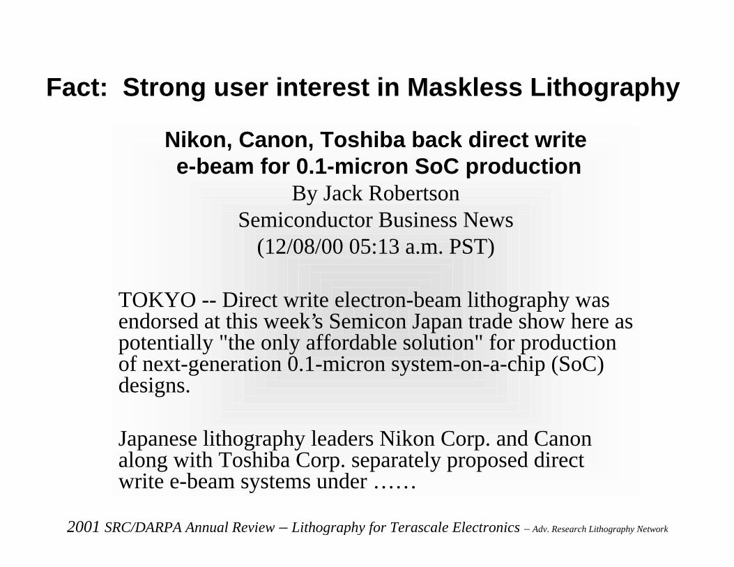
Nikon, Canon, Toshiba back direct write e-beam for 0.1-micron SoC production
By Jack RobertsonSemiconductor Business News
(12/08/00 05:13 a.m. PST)
TOKYO -- Direct write electron-beam lithography wasendorsed at this week’s Semicon Japan trade show here aspotentially "the only affordable solution" for productionof next-generation 0.1-micron system-on-a-chip (SoC)designs.
Japanese lithography leaders Nikon Corp. and Canonalong with Toshiba Corp. separately proposed directwrite e-beam systems under ……
Fact: Strong user interest in Maskless Lithography
2001 SRC/DARPA Annual Review – Lithography for Terascale Electronics – Adv. Research Lithography Network

What is Status of Commercial Maskless Lithography?
Existing Products
Cell and Character Projection E-beam (Hitachi andAdvantest, respectively)
< 1 W/hr
> 150nm
High-resolution e-beam (Jeol, Hitachi, Leica)
<<0.1W/hr (but very high resolution)
Low resolution Optical (e.g. Intelligent Micro Patterning)
2001 SRC/DARPA Annual Review – Lithography for Terascale Electronics – Adv. Research Lithography Network

What is Status (continued) ?Intended Products
Ion Diagnostics multicolumn e-beam (6432 beamlets)
Funding ran out – now aimed at inspection
Etec “Microcolumn multi e-beam” (148 – 624 columns)
Still alive, but in very early stage of development
Micronic Eximer-based “DLM” writer
~ 250nm resolution evolving to 150nm node
~ 106- 107 mirrors
~ 5-10 W/hr goal
Canon, Toshiba direct write e-beam2001 SRC/DARPA Annual Review – Lithography for Terascale Electronics – Adv. Research Lithography Network

Maskless Lithography: Opportunities
Direct writing exhibits the nearest term potentialfor prototype and development work.
With exponentially rising mask costs, @$0.5M/settoday, will maskless lithography be viable for:
• Mask patterning?
• Low volume ASIC testing?
• High volume manufacturing?
Harry LevinsonSRC Summer Study 2001

Maskless Lithography: Research Issues
Energy sources*
Data Delivery: data path architecture and implementation*
Write engine: best hardware and architecture?*
Infrastructure: resists, CAD, technology, memory, computation speed, and communication*
* Research supported by SRC/DARPA
WGO SRC Summer Study 2001
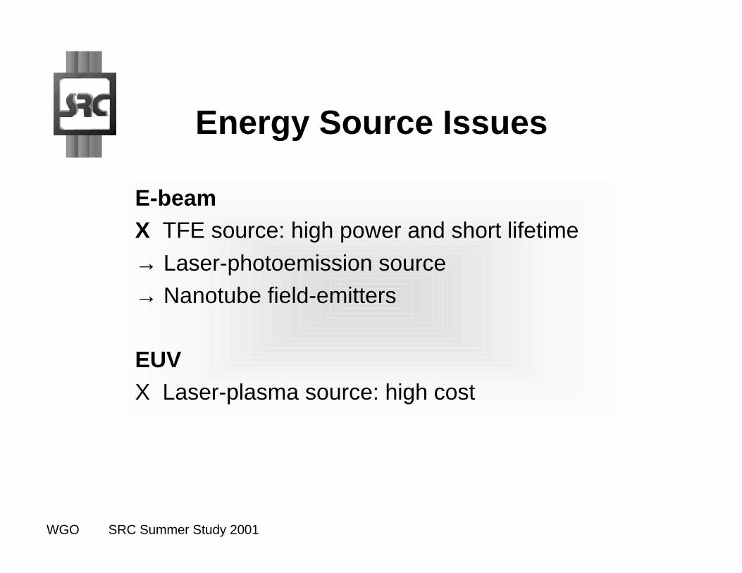
Energy Source Issues
E-beamX TFE source: high power and short lifetime
→ Laser-photoemission source→ Nanotube field-emitters
EUVX Laser-plasma source: high cost
WGO SRC Summer Study 2001

Data Delivery Challenge
Assumptions:
Gray Scaling (about 20X penalty over MFS grid)
10cm2/sec write speed (~50 300mm wafers/hour)
No overhead
MFS = 100 n m
Raster Scan 100% Coverage (“bit map”)
BIT RATE = 20 X 10 /(100 X 10-7)2 = 2 x 1012 bits/sec
Compression is required!
WGO SRC Summer Study 2001

Write Engine
Two Examples
•“Line Scan” using continuous source
•“Flashing Illuminator” using pulsed source
Both examples use same assumptions of last slide
WGO SRC Summer Study 2001

“Line Scan” using continuous source
LineScan
BrushScan
WobbleScan
RedundantScan
Assume maximum stage speed of 100cm/sec
Assume requirement of 10cm2/sec: at 100cm/sec 0.1cm scan width
Assume 50nm spot size 2 X10⁴ beams modulated at 100MHz
(or fewer “wobbled” beams modulated faster)
Redundancy requires more beams
Multipass requires more beams and/or faster scan
WGO SRC Summer Study 2001

Flash on Fly (pulsed source)*
* ( See USP 5,691,541)
Assume maximum pulse rate of 10 kHz
10cm2/sec at 104 flashes/sec 10-3 cm2/flash
10-3 cm2/flash at 50nm spots 4 x 10⁷ spots/flash
Redundancy requires even greater number of elementsper flash
Etc.
Flash1 Flash 2 Flash 3
WGO SRC Summer Study 2001

Maskless Lithography: Network Research Vectors
Scanning Probes: Demonstrate lithographic patterning withlarge arrays of probes scanning simultaneously, demonstratedurability of tips
Multiaxis E-beam: Determine limits and performance potential ofseveral novel approaches including multi-column shaped-beam,and NEA photocathode arrays
EUV: Demonstrate viability of fabrication approaches, mechanicaland thermal viability of sub-micrometer mirrors using bothdeflection and phase-modulation approaches
Droplet-on-Demand: Determine limits and performance of drop-on-demand jet printing and investigate applications to low-costelectronics
Data Path and Circuitry: Analyze tradeoffs in compressionefficiency and on-chip decoding complexity & estimate feasibilityand circuit complexity as limited by space and power dissipation.
2001 SRC/DARPA Annual Review – Lithography for Terascale Electronics – Adv. Research Lithography Network
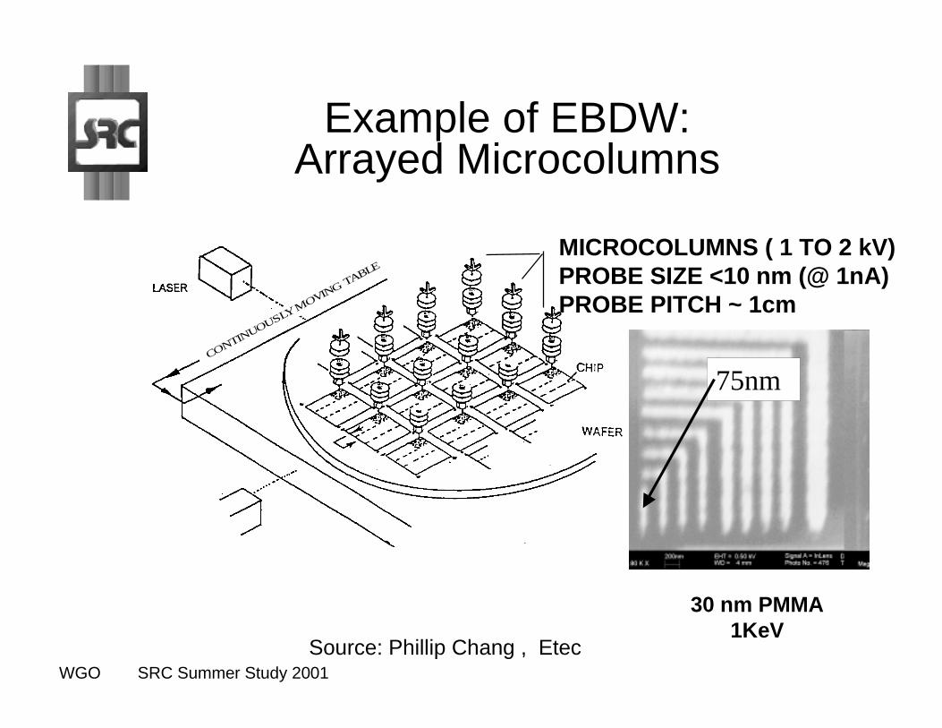
Example of EBDW:Arrayed Microcolumns
CONTINUOUSLY M
OVING TABLE
MICROCOLUMNS ( 1 TO 2 kV)PROBE SIZE <10 nm (@ 1nA)PROBE PITCH ~ 1cm
Source: Phillip Chang , Etec
30 nm PMMA1KeV
75nm
WGO SRC Summer Study 2001

Direct Write with Proximal ProbeZnO / PR Cantilever Design
Source: Quate group, StanfordWGO SRC Summer Study 2001

DIVA
Distributed Axis ElectronBeam Lithography
Stanford University2001 SRC/DARPA Annual Review – Lithography for Terascale Electronics – Adv. Research Lithography Network

2001 SRC/DARPA Annual Review – Lithography for Terascale Electronics – Adv. Research Lithography Network

Direct Write with EUV:The concept
Source: Oldham group@ Berkeley & Dave Markle@ Ultratech
“Electronicmask”
“Electronic mask” is anarray of tiny mirrors (105 -108 mirrors)
WGO SRC Summer Study 2001

Elastomer
electrode
electrode
Reflective multilayer
2µm
0.2µm
1µm
1µm
Silicon Substrate
0.6µm
N
N
MolybdenumSilicon
81 layersR~70%
4 nm
2.8 nm
MolybdenumSilicon
MolybdenumSilicon
EUV Maskless Lithography
Structure of ElastomerSLM
2001 SRC/DARPA Annual Review – Lithography for Terascale Electronics – Adv. Research Lithography Network

Operational Principle
When all of the pillars are of the sameheight, the incident light is specularlyreflected
When the difference between adjacentpillars is 1/4 λ, all of the light isdiffracted and a dark pixel is formed
The simple structure of the pixelsallows scaling to large arrays
2001 SRC/DARPA Annual Review – Lithography for Terascale Electronics – Adv. Research Lithography Network

Fabrication of Comb-Structure Nanomirrors
R
VB+vm
HingeUnpolished Mirror
2001 SRC/DARPA Annual Review – Lithography for Terascale Electronics – Adv. Research Lithography Network

Maskless Lithography for Low-Cost Electronics
Inkjet System Inkjet System
The Holy Grail: Reel-to-Reel Fab
Low cost – no clean rooms, cheap substrates
2001 SRC/DARPA Annual Review – Lithography for Terascale Electronics – Adv. Research Lithography Network

More examples of Direct-Write approaches
Zone-plate lithography (ZPAL): MIT
Droplet-on-Demand (“resist jet”) Lithography: Berkeley
Near-field optical lithography: Stanford
Maskless ion-beam lithography: Berkeley
Each is a massively parallel array of writers
WGO SRC Summer Study 2001

Data Flow Management:Specifications
1.6 TBitsChip data(one layer)
10mm x 20mmChip size
9.4 TBits persecond
Data rate60 secondsWriting time(one layer)
560 TBitsWafer data300 mmWafer size
5 bits / 32 grayPixel depth< 1 nmEdge placement
25 nmPixel size50 nmMinimum feature
Direct-writeDevice
2001 SRC /DARPA Annual Review – Lithography fo r Te rasc ale Ele c tronic s – Adv. Re se arch Lithography Ne twork

Projected Compression Needs
According to 2000 ITRS:I/O bandwidth and required data rate diverging, i.e. compression ratio growing128 pins at 3.125 Gb/s possible by the end of 130 nm generation
I/O Bandwidth Vs Data Rate for various feature sizes
1.00E+122.10E+134.10E+136.10E+138.10E+131.01E+141.21E+141.41E+141.61E+141.81E+14
050100150200Minimum Gate Length (nm)
Bit
s/s
Compression Ratio Required over Generations
0
2
4
6
8
10
12
14
16
18
050100150200Minimum Gate Length (nm)
Co
mp
ress
ion
Rat
io
2001 SRC /DARPA Annual Review – Lithography fo r Te rasc ale Ele c tronic s – Adv. Re se arch Lithography Ne twork

Lossless Layout Compression for MasklessLithography Systems:
50 NM Node System Architecture
Throughput from processor board to on-chip decompress islimited (1000 pins at 400 MHz or 128 pins at 3.125 GHz)
Real-time decompression must be done with limited on-chipcircuitry; no rasterization
!"###
"$"% % "&%
!"##
2001 SRC /DARPA Annual Review – Lithography fo r Te rasc ale Ele c tronic s – Adv. Re se arch Lithography Ne twork

Compression Results
900 KB200 KB4 KBDecoder buffer requirements:
72.8
24.5
18.7
61.1
33.9
Rectangle
145
273
328
144
111
2D-LZ
47.3
60.1
46.4
61.1
45.7
ZIP(LZ77)
> 2D-LZ
> 2D-LZ
> 2D-LZ
> 2D-LZ
> 2D-LZ
BZIP2(BWT)
active_e
active_d
active_c
active_b
active_a
Layout
9.37
7.44
5
9.69
8.44
SPIHT
* Compression results over a 2000 x 2000 block of 5-bit gray data
2001 SRC /DARPA Annual Review – Lithography fo r Te rasc ale Ele c tronic s – Adv. Re se arch Lithography Ne twork

####''' ''()
WritersDecomp.
I/O => 128 pins@ 3.125 Gb/s Demux
+ Buffer
16000 Parallel decompression paths
Writers built on compact memory array16000 x 16000
25mm
25mm
Chip Architecture
Maskless Lithography Data Path Design
2001 SRC /DARPA Annual Review – Lithography fo r Te rasc ale Ele c tronic s – Adv. Re se arch Lithography Ne twork

Maskless lithography, direct write, appears to offerpotential solutions that could co-exist with NGL systems.
Compatibility with the emerging NGL infrastructure will becompelling (EUV vs. e-beam).
Both the writing engine and the data-path /processingarchitecture are key areas for research. => β tool 5-7 yrs.
I/O bandwidth is biggest concern, low power circuit designcan reduce power consumption to reasonable levels
Data flow management challenges will impact insertionoptions, such that maskless lithography likely will writemasks and test ASICs before entering IC manufacturing
Summary
WGO SRC Summer Study 2001

MASK PATTERNING PRODUCT GROUPMASK PATTERNING PRODUCT GROUP
3835 032901-JV (BAA 97-07 110100 KYL)
1
Multi-ebeam Direct Write(MEBDW)
Mark Gesley
Aug 28, 2001SRC/ISMT Direct Write
Workshop

MASK PATTERNING PRODUCT GROUPMASK PATTERNING PRODUCT GROUP
23835 032901-JV (BAA 97-07 110100 KYL)
Purpose of presentation
! Review current progress in Multi-ebeam Direct Write (MEBDW)
! Assess what is necessary to implement the technology for 50/35nm manufacturing
! Identify what SRC/ISMT can do to facilitate technology development

MASK PATTERNING PRODUCT GROUPMASK PATTERNING PRODUCT GROUP
33835 032901-JV (BAA 97-07 110100 KYL)
Outline
! A few assertions! System architecture considerations! Features and benefits: extended array printing! Risks: module technology/system engineering/product-
application! Concept and feasibility targets! Progress to date! Timing of 50/35 nm insertion to manufacturing! Conclusion/Recommendations

MASK PATTERNING PRODUCT GROUPMASK PATTERNING PRODUCT GROUP
43835 032901-JV (BAA 97-07 110100 KYL)
A few assertions that influence the best path to MEBDW
! Acceptable throughput is that which will obtain sufficient salesfor the required ROI– not necessarily set only by comparison to wafer stepper throughput– such comparisons set unrealistic throughput targets/expectations
which can lead to incorrect technology choices
! Cost-of-ownership will determine minimum acceptable throughput as set by the– price/complexity/existence of the wafer stepper– price/complexity/existence of the mask– number of wafers to be printed with that mask.

MASK PATTERNING PRODUCT GROUPMASK PATTERNING PRODUCT GROUP
53835 032901-JV (BAA 97-07 110100 KYL)
System architecture considerations
! Multi-ebeam is the only path to achieve acceptable throughput– Single beam technology will not do better than < ¼ wph (at 100nm)
! Vector-scan multi-ebeam is not feasible for direct write– Insufficient control of multibeam brush printing or multiple datapaths
required
! Raster multi-ebeam architecture provides– lower positional errors via repetitive scanning– necessary bandwidth and channel capacity of data handling – digital resolution extension through gray printing

MASK PATTERNING PRODUCT GROUPMASK PATTERNING PRODUCT GROUP
63835 032901-JV (BAA 97-07 110100 KYL)
Technical attributes: Microcolumns for MEBDWFeature BenefitUses gray level,multipass, Gaussian beamprint strategy
Extends existing writing /calibration strategies
Extended array ofbeamlets
Throughput-resolution extendibilityby # beamlets and density. Lowersstage velocity
No crossover in brush Resolution without throughputpenalty
Low voltage printing Simpler datapath: no proximity orheating correctionsEnhanced resist sensitivity
Thin layer imagingprocess/lithography
EUV addressing similar Process,etch, defect issues
TFE-cathodes/gun Dose stability, commerciallyavailable

MASK PATTERNING PRODUCT GROUPMASK PATTERNING PRODUCT GROUP
73835 032901-JV (BAA 97-07 110100 KYL)
Risks
! Module technology– array stability: position, dose, lifetime– TLI process: immunity to contamination and drift
• Resist/etch selectivity limits of pattern transfer
! System engineering– printing/calibration/diagnostic complexity;– datapath implementation– mark finding/alignment
! Product timing for 50/35 nm! Product configuration
– application development– requirements, implementation and use/ beta partnership

MASK PATTERNING PRODUCT GROUPMASK PATTERNING PRODUCT GROUP
83835 032901-JV (BAA 97-07 110100 KYL)
Concept and feasibility targets for 50/35 nm
! Reduce module risks– 320 MHz electronics, interconnect integrity– Robust, long-lived source and immunity to contamination and drift
! Demonstrate 50 nm array lithography capability on small 100 µm fields– 4-beam patterning and control– CD and placement accuracy with thin layer imaging and etch– Mark alignment capability
! Achieve full 50 nm mask patterning capability with 16 beams ! Address MEBDW system complexity concerns
– Throughput at <<10 hr– Datapath capacity and bandwidth– Lithography quality using extended array printing
! Establish market requirement specifications

MASK PATTERNING PRODUCT GROUPMASK PATTERNING PRODUCT GROUP
93835 032901-JV (BAA 97-07 110100 KYL)
Progress to date
! System concept! A key subsystem: the raster bit-mapped datapath! Module-level
– microcolumn optics– packaging-interconnect
! Test stand! Lithography results

MASK PATTERNING PRODUCT GROUPMASK PATTERNING PRODUCT GROUP
103835 032901-JV (BAA 97-07 110100 KYL)
MFS 50 nm (half pitch) Fixed Pixel Rate 300 MHz (Variable wafers per hour)MIFS 30 nm (gates)
Design assumptions: Parallel calibration of columns on master plate in tool " 40-second calibration done once per wafer " Blanker amplifier rise times ~ 200 ps " 36-second load/unload and registration time
Column footprint, mm 20 × 20 10 ×10 5 × 5Number of inscribed columns 148 624 2632
Shaped Beam (1 pass)Max flash size (pixels/scan) 50 (1024) 50 50Scan length, µm 51.2 51.2 51.2Pixel rate, MHz 300 300 300Amps/col, nA (1 µC/cm2) 8.9 6.2 2.8Stage speed, mm/sec 14.7 10.2 4.6Write time (cycle time), min 9 (10.2) 2.4 (3.5) 0.6 (1.8)Wafers per hour 6 17 33
MEBDW System Concept 50/35 nm

MASK PATTERNING PRODUCT GROUPMASK PATTERNING PRODUCT GROUP
113835 032901-JV (BAA 97-07 110100 KYL)
A Key Subsystem: The Raster Bit-mapped Data Path
Patternstore
Large memory
Low bandwidthSmall memory
High bandwidth
Variables Store Memory size Buffer size Number ofchannels
Rastersection
Memorysection
Columnbuffers
Rasterbandwidth

MASK PATTERNING PRODUCT GROUPMASK PATTERNING PRODUCT GROUP
123835 032901-JV (BAA 97-07 110100 KYL)
MEBDW Data Path Feasibility Study
! With commercially available parts, data delivery to the direct write tool has a throughput capacity of 10 wafers/hr under the following conditions– 300 mm wafer, ~600 columns– 25 nm printing pixel – Four data pixels per 50 nm beam flash at 125 MHz– No real-time corrections applied to the data – 25 × 44 mm maximum chip size

MASK PATTERNING PRODUCT GROUPMASK PATTERNING PRODUCT GROUP
133835 032901-JV (BAA 97-07 110100 KYL)
Test stand lithography with single microcolumn
" 100µµµµm exposure field" 25nm thick PMMA" Blanker errors observable" ~250 nm (2 pixel) MFS

MASK PATTERNING PRODUCT GROUPMASK PATTERNING PRODUCT GROUP
143835 032901-JV (BAA 97-07 110100 KYL)
! Infineon’s CARL bilayer resist– Established manufacturing technology
• Since 1995, with >80,000 wafer starts for 0.5 mm lithography using i-line– Process
• Image and wet silylate top imaging layer• Dry develop bottom hardened novolac layer
35 nm
250 nm
70 nm features in 35/250 nm CARL
! Preliminary 1 kV e-beam CARL results
– Sensitivity ~2 µC/cm2
– Contrast >10– High resolution: 70 nm features
in 35/250 nm resist – With ~5 nm beam, ∆CD/∆dose
<0.5 nm/%dose– Linearity: range 7 nm– No proximity effects
70 nm Resolution / 1 kV exposure

MASK PATTERNING PRODUCT GROUPMASK PATTERNING PRODUCT GROUP
153835 032901-JV (BAA 97-07 110100 KYL)
! 85 nm linewidth: Tower PatternLinewidth @ 2.6 µC/cm2
85 nm
85 nm
85 nm
10 mm
1 kV CARL: No Proximity Effect

MASK PATTERNING PRODUCT GROUPMASK PATTERNING PRODUCT GROUP
163835 032901-JV (BAA 97-07 110100 KYL)
40 nm resolution: HSQ
1 kV exposure. Dose ~20 µC /cm2. Courtesy A. Jamison/ U. Texas

MASK PATTERNING PRODUCT GROUPMASK PATTERNING PRODUCT GROUP
173835 032901-JV (BAA 97-07 110100 KYL)
CY 2001 2002 2003 2004 2005 2006 2007 2008 2009 2010SIA 3/99
Generation (nm) 130 100 70 50
AcceleratedTwo-year Cycle 100 70 50
Technology Development • 16 multi-e-beams • 100–70 nm capability
• 64 beam• 70 nm capable
Product DevelopmentMEBDW • 50 nm • 256 beam
• First beta
Commercialization
• 256 beam• 70 nm capable
• 10 units/year• 100 units/year
Timing risk: MEBDW
Identify key technical hurdlesIdentify key technical hurdles"" Throughput (extendibility)Throughput (extendibility)"" Alignment Alignment
$$ StitchingStitching%% Mark detectionMark detection%% ColumnColumn--column stabilitycolumn stability
"" ReliabilityReliability

MASK PATTERNING PRODUCT GROUPMASK PATTERNING PRODUCT GROUP
183835 032901-JV (BAA 97-07 110100 KYL)
Risk: Product configuration! Partnership with integrated device manufacturer is
needed for– Successful insertion into manufacturing– Risk reduction and R&D leverage
! Ω-partner needs data and understanding of issues– Lengthy adoption of technology and market penetration– Joint tasks are complementary to those needed for advanced
mask patterning– Helps us understand multibeam patterning technology
! What can be done now by the Ω-partner?– Pattern transfer technology (process development)– Definition of requirements and experiments

MASK PATTERNING PRODUCT GROUPMASK PATTERNING PRODUCT GROUP
193835 032901-JV (BAA 97-07 110100 KYL)
Conclusions/Summary! Progress to date
– System concept/datapath developed – Unit microcolumn characterized: optics, package, interconnect– TLI process data: 40~70 nm resolution w/ no proximity effect
! Challenges ahead– Array system complexity: calibrations/diagnostics/writing– Applications development and impact on system requirements
! Milestones to manufacturing implementation– Existence as a mask pattern generator– Partnership between tool supplier and device manufacturer
! What can SRC/ISMT do?– Promote/support TLI process development
• Resist, Etch, Defect characterization

MASK PATTERNING PRODUCT GROUPMASK PATTERNING PRODUCT GROUP
203835 032901-JV (BAA 97-07 110100 KYL)
Acknowledgements
! DARPA/NAVAIR/SPAWARS support of microcolumntechnology development
! Microcolumn development team! Andrew Jamison, Univ. Texas (HSQ development)

2001.08.28Semiconductor Production Equipment Development Center
The present status ofThe present status ofCanonCanon’’s ML2 technologys ML2 technology
Nobuyoshi Deguchi Nobuyoshi Deguchi of Canon Inc. of Canon Inc.

2001.08.28Semiconductor Production Equipment Development Center
1. Canon1. Canon’’s strategy of NGLs strategy of NGL DevelopmentDevelopment2. Canon2. Canon’’s approach to ML2s approach to ML2
- Background - Background - Aberration Correction technology (CLA System) - Aberration Correction technology (CLA System)
- Key Technologies / Multi EBDW - Key Technologies / Multi EBDW - ML2 Tool Development Schedule - ML2 Tool Development Schedule
3. ML2 development status report3. ML2 development status report
- CLA development status- CLA development status - Air-guided wafer stage development status - Air-guided wafer stage development status
4. Conclusion4. Conclusion
Outline Outline

2001.08.28Semiconductor Production Equipment Development Center
CanonCanon’’s strategy of NGL Development s strategy of NGL Development
EUV
100nm 50nm70nm
SoC Market QTAT
MEBDW(ML2)
F2KrF ArFI-line
150nm300nm
Current = 130nm Final Goal
70nm
Mask-less system

2001.08.28Semiconductor Production Equipment Development Center
Mask-Less is alternative solutionMask crisis : Accuracy, MEF, OPC -> impact to mask manufacturing -> Cost Rising mask cost gives serious damage to devices of SoC( Many products/Low volume )
Expo
sure
Cos
t (A.
U)
0
5
10
15
20
25
30
35
40
200 500 1000 2000 5000 10000 50000
6"4x6"6x7"6x
Reticle & Magnif. 12x12mmChip
3.5 9 18 35 90 180 900
Total chip product amount (unit 10,000)
Tool model-3Tool model-2Tool model-1KrF (130nm)
0
10
20
30
40
50
60
250 500 1000 2000 4000 8000 16000 32000 64000
Expo
sure
Cos
t (A.
U)
25 50 100 200 400 800 1600 3200 6400 Total chip product amount (unit 10,000)
Reticle & Tool 12x12mmChip
Features Features – Multi-EB direct write system Mask-less– Large field size and High NA High-Throughput– New correction technique High Resolution

2001.08.28Semiconductor Production Equipment Development Center
1. Canon1. Canon’’s strategy of NGLs strategy of NGL DevelopmentDevelopment2. Canon2. Canon’’s approach to ML2s approach to ML2
- Background - Background - Aberration Correction technology (CLA System) - Aberration Correction technology (CLA System)
- Key Technologies / Multi EBDW - Key Technologies / Multi EBDW - ML2 Tool Development Schedule - ML2 Tool Development Schedule
3. ML2 development status report3. ML2 development status report - CLA development status- CLA development status
- Air-guided wafer stage development status - Air-guided wafer stage development status
4. Conclusion4. Conclusion
Outline Outline

2001.08.28Semiconductor Production Equipment Development Center
Parameters of the MEBDW system
Accelerating voltage (kV) 50 Energy spread (eV) 2 Demagnification ratio 50 Convergence angle (mrad) 10 Individual beam size (nm) Φ 17.5 Number of beams 4096 (64x64) Main-field size (um x um) 4.096 x 0.256 Sub-field size (um x um) 256 x 256 m-field size (um x um) 4 x 4 Focal length of the final lens[Lens D] (mm) 20 Focal length of the correction lens (mm) 100

2001.08.28Semiconductor Production Equipment Development Center
LaB6 ( Uniformity of radiation angle, emission stability )
Low distortion Magnetic Lens
High sensitive Resist for higher Throughput
Giga-scale Mask data handling
Charge Up measures, In-Situ Cleaning
Stitch and Alignment, Multi Beam drift control
Blanking Aperture Array, Correction Lens Array, Multi Deflector
High accuracy Air-guided wafer stage in HV
EB Source
Lens Design Lens Design
Resist
Virtual Mask
Manufacturing Manufacturing
StageStageEnvironmentEnvironment
AlignmentAlignment
Lens Device
Key Technologies / Large Field Key Technologies / Large Field MEBDWMEBDW

2001.08.28Semiconductor Production Equipment Development Center
Overhead time : 30 sec/8”waferResist sensitivity : 3 uC/cm2
Pattern density : 50 %Exposed area of a wafer : 240 cm2
Lens aberration blur sab : standard deviation of aberration disk
Simulated Throughputs CLA system
Image blur Lens aberrations blur sab 13.7 components Optical assembly tolerance blur stol 10.0
(nm) Depth of focus blur sfoc (DZ=+/-1um) 5.8 Allowable image blur stotal for 70% contrast (nm) 33.8
Resolution Coulomb Interaction blur (nm) 28.7100nm Total current (mA) 11.8
Throughput (8"wafers/ hour) 59 Allowable image blur stotal for 70% contrast (nm) 23.6 Coulomb Interaction blur (nm) 15.4
Resolution Total current (mA) 4.870nm Throughput (8" wafers/ hour) 34
Allowable image blur stotal for 50% contrast (nm) 29.9 Coulomb Interaction blur (nm) 23.9 Total current (mA) 9.1 Throughput (8" wafers/ hour) 52

2001.08.28Semiconductor Production Equipment Development Center
Field
size
Convergenceangle
Multi-source
Opt
ics
Maximize the throughput for a given resolution
A much lager field sizeA much lager convergence angle (NA)
New corrections is required
Minimize the Coulomb interaction effect
Increasing lens aberrations
EB lithography tools : Throughput is limited by the Coulomb interaction effect
Background of CLABackground of CLA

2001.08.28Semiconductor Production Equipment Development Center
Final Image Field
Intermediate Image Field
Distortion
Aberration Correction
Projection Optics
CLA
Electron source
BAA
Field Curvature
Collimator Lens
Image of source
Electron source
ApertureDeflector
Lens 1
Lens 2
Principal Plane
Correction lens
Collimator lens
Fc
Correction lens
Correction lens

2001.08.28Semiconductor Production Equipment Development Center
MEBDW Tool Development ScheduleMEBDW Tool Development Schedule
System research & Design
EB Optics Design
Basic elements CLA device EB gun Vacuum Stage in HV
Fabrication
Assembly/DBG
Evaluation
ProductionTool
(2nd Version)
tool(1st Version)
2001 2002 2003 2004 2005 2006 2007

2001.08.28Semiconductor Production Equipment Development Center
1. Canon1. Canon’’s strategy of NGLs strategy of NGL DevelopmentDevelopment2. Canon2. Canon’’s approach to ML2s approach to ML2
- Background - Background - Aberration Correction technology (CLA System) - Aberration Correction technology (CLA System)
- Key Technologies / Multi EBDW - Key Technologies / Multi EBDW - ML2 Tool Development Schedule - ML2 Tool Development Schedule
3. ML2 development status report3. ML2 development status report
- CLA development status- CLA development status - Air-guided wafer stage development status - Air-guided wafer stage development status
4. Conclusion4. Conclusion
Outline Outline Outline Outline Outline Outline Outline Outline

2001.08.28Semiconductor Production Equipment Development Center
Lens Array Lens Array
100m
50m
100m
200mEinzel Lens
3rd
Electrode
1st Electrode
2nd Electrode
80m

2001.08.28Semiconductor Production Equipment Development Center
Principle of CLA
ThreeElectrodesVoltages applied
ElectronBeam
1st electrode
2nd electrode
3rd electrode
Equipotential line

2001.08.28Semiconductor Production Equipment Development Center
Photo of the lens array
50mm
Lens holder
Pin
1st substrate
1st electrode with shield membrane
2nd substrate2nd electrode
Base substrate

2001.08.28Semiconductor Production Equipment Development Center
Experimental setupfor Hartmann`s test
Electron beam
Hartman aperture
FC
Vc
Screen1
Screen2
gun
CL
OLUD
LD
Lens array
(estimation of the focal length)

2001.08.28Semiconductor Production Equipment Development Center
Details of Hartmann’s test
Hartmann`saperture
Lens
SC1
SC2
Lens OFF
Lens ON
h1
h2
30m-pencil
15m
30mElectron Beam
15m-pencil
(30m-pencil)
(30m-pencil)

2001.08.28Semiconductor Production Equipment Development Center
Result of Hartmann’s test(focal length of pencils)
(absolute value)Acceleration Voltage ; 10kV

2001.08.28Semiconductor Production Equipment Development Center
Prototype Wafer stagefor High Vacuum Circumstance
Prototype Vacuum StagePrototype Vacuum Stage

2001.08.28Semiconductor Production Equipment Development Center
ConclusionConclusion
• “Mask-less Lithography” is a key word forsmall volume production.
– CLA can solve the aberration problems of highthroughput EB optics.
• CLA device development status– Small sized lens array has been fabricated.– Lens array is under evaluation.
• Wafer stage development status– The first trial wafer stage for the vacuum circumstance
have been fabricated.– We are developing the improved wafer stage.

1 Maskless Lithography 2001
The Maskless Stepper - a Flashy New Tool
Tor SandstromMICRONIC Laser Systems

2 Maskless Lithography 2001
The Maskless Stepper (MLS)- Maskless Lithography with a Difference
Not aiming to solve the NGL quandary
An opportunity to build a maskless lithography system which
prints identically to an optical stepper
uses files on a hard-disks instead of reticles has close to perfect process compatibility
with the steppers
Current status: an ongoing joint design and market study
by
- pattern generators
- stepper technology

3 Maskless Lithography 2001
Micronics maskwriter development
OMEGA laser-scanning reticle writer
New SIGMA SLM-based reticle writer
resolution: 180 nm
registration: 25 nm
CD uniformity: 10 nm
Voting: 4 pass
write time: 2-3 hours

4 Maskless Lithography 2001
SLM-based pattern-writing
New deep-UV SLM-based technology for writing reticles
uses a micromirror chip as a computer-controlled reflective reticle
imaging physics is identical to a DUV stepper
can use 248, 193, 157, ... nm
throughput is onlybounded by practicallimitations of SLMtechnology and dataprocessing
SLM
Beamsplitter
Light from excimer laser
Substrate
Fine StagePCB
High Speed Data Link
Data Handling
Unit
SLM = Spatial Light Modulator

5 Maskless Lithography 2001
Principle of operation
SLM chip
Fourierfilter
Reductionlens
Maskblank
Fourierlens
Laserpulse
Beam-splitter
0001111110000data
The optics of a stepper, but... much higher
demagnification
a reflective SLM chip in the place of the reticle
the SLM diffracts lightaway from the lens aperture where non-zero data is loaded
Flash-on-the-fly: a continuously moving stage
a 20 ns long excimer laserpulse illuminates the SLM and prints an image of the SLM on the workpiece
the SLM data is reloaded in time for the next flash, 1000 times per second or more

6 Maskless Lithography 2001
Not invented here...
SLM chip
Fourierfilter
Reductionlens
Maskblank
Fourierlens
Laserpulse
Beam-splitter
0001111110000data
The excimer-based flash-on-the-flypattern generator was invented by Dr. Heinz Kück at the Fraunhofer Institute for Microelectronic Circuits and Systems in Duisburg.

7 Maskless Lithography 2001
Using diffraction to create contrast with < 0.1 µm of mirror movement
When the SLM surface is flat all light is reflected in the specular direction
A very small surface perturbation causes the light to be diffracted and the specular reflection is attenuated or extinguished
Variable attenuation by variable non-flatness enables analog addressing for gray scale

8 Maskless Lithography 2001
The micromirror SLM chip
Torsional 16 x 16 micronmirrors
The mirrors are actuated by electrostaticforce
A matrix-addressed CMOS chip similar to a TFT screen below the mirrors
Mirror array
M
E
C T
A1 A2 A3 A4
G1
G2
G3
Matrix addressing of analog array
0.062 µm
16 µm

9 Maskless Lithography 2001
The SLM is designed to work exactly as a binary mask, but with 64-level gray
+/- 0.00 µm +0.34 µm defocus+0.17 µm
robust imaging with no phase effects in the image
stability through focus
X-Y symmetry
400 nm feature through focus
Mirror height map

10 Maskless Lithography 2001
1 Mpixel Analog Spatial Light Modulator
Developed by the Fraunhofer Institute of Microelectronic Circuits and Systems, Dresden. Ackn: Hubert Lakner, Peter Dürr

11 Maskless Lithography 2001
Micromirror Details

12 Maskless Lithography 2001
Mask Clear - Dark Isolated Lines
SLM imaging248 nm wavelength
200 nm (208)300 nm (296)400 nm (401)500 nm (510)600 nm (591)
February 2001

13 Maskless Lithography 2001
Starburst with 0.3 µm spokes- data and SEM picture
Blue: deflected = dark
White: relaxed = bright
Other colours = intermediate analog deflections

14 Maskless Lithography 2001
SLM
Beamsplitter
Light from excimer laser
Substrate
Fine StagePCB
High Speed Data Link
Data Handling
Unit
All my friends
print on silicon ...
Hey,I am a
stepper !

15 Maskless Lithography 2001
SLM
Beamsplitter
Light from excimer laser
Substrate
Fine StagePCB
High Speed Data Link
Data Handling
Unit
Nobodywould notice
the difference
!
Why cant I print on wafers
like the big guys ?

16 Maskless Lithography 2001
Stepper/Scanner
Wavelength: 248 nm
NA: 0.75
Sigma: 0.3-0.8
Annular, quadrupole, dipole illumination
Attenuated PSM
Strong PSM
Resist
SLM-based Maskless Tool
same
same
same
same
same
option
same
SLM
Beamsplitter
Light from excimer laser
Substrate
Fine StagePCB
High Speed Data Link
Data Handling
Unit
Look here...

17 Maskless Lithography 2001
Wait a minute !
The delay timesare not the
same

18 Maskless Lithography 2001
Identical process - except for the delay times
The maskless tool is one-two orders of magnitude slower than a stepper/scanner
Writing time is 5 -30 minutes, not 30 seconds
Manual handling of wafers in low volume adds issues with contamination and varying delays
CD control could be affected
Therefore:
the MLS must be interfaced to a track
workflow and delay times must be actively managed
the AMB contamination must be well under control
it may not be optimal to write full wafers
If this issue is kept under control you have a perfect match between reticle stepper/scanner and maskless stepper

19 Maskless Lithography 2001
Throughput
The throughput of a modern stepper with 120 WPH @ 300 mm and 110 nm L/S corresponds to 1000 billion gray-scale pixels per second, or 1000 Gpel/s
Micronics current SLM engine prints 1 Gpel/s
Does a slow tool have a market?
Yes, even a slow tool that produces expensive wafers can save time and money!

20 Maskless Lithography 2001
How can a slow and expensive tool save time and money?
Use value Value per wafer:
based on selling price
Proportional to productionvolume
Memories, MPUs, ASICs, etc.
Intellectual value Value per wafer:
based on knowledgeand timing, can be very high
Independent of volume
Customer samples, engineering prototypes, redesign confirmations, design iterations, parameter mapping, process development experiments
Because wafers have two types of value:

21 Maskless Lithography 2001
Half of all reticles print only one wafer lot
From J Schmitz, Philips, SEMICON Europe 2001

22 Maskless Lithography 2001
Economy of replacing reticles
If you only need one state-of-the-art wafer to confirm a design, that wafer may cost 500,000 $ in reticle cost
Writing it in a maskless tool for 100 000 $ would be a bargain.
At 10 000 $ per wafer you are in the realm of profitable small-volume production
For best economy only some layers are maskless, since non-critical reticles are inexpensive, quick to get and are used late in the process.
Optimizing within the maskset extends the economic use of maskless lithography to more products, but with fewer substituted reticles in each maskset

23 Maskless Lithography 2001
The cost is doubly high for the critical layers
critical
subcritical
non-critical
dominates:- performance
- cost- time to market
Cost of reticle lead time

24 Maskless Lithography 2001
At some limit maskless becomes desirable
Cost of reticle lead time
critical
subcritical
non-critical
ML better
Reticlesbetter
2 WPH
10 WPH

25 Maskless Lithography 2001
A mix of masksets
Cost of reticle lead time
ML betterReticlesbetter

26 Maskless Lithography 2001
Design study - basics
300 mm wafers per hour: 2
Lines: 130 nm
L/S: 130 nm
NA: 0.75
Wavelength: 248 nm
Sigma: 0.3 0.9 variable pattern
Projected pixel size: 50 x 50 nm
Address grid: < 1 nm
Pixels per second: 30 Gpel/s, double-pass

27 Maskless Lithography 2001
Focus on CD control
CD control is paramount. No tool is good enough on CD control.
For maskless lithography we are implementing:
2-pass voting
field blending
flash energy correction
analog calibration of every mirrors transfer function
Data integrity and rasterizing accuracy is an absolute requirement
1
2
y
x
Two-pass voting with offset fields
Field blending using the analog modulation
y
x

28 Maskless Lithography 2001
Individual mirror correction
All mirrors are characterized optically. Their transfer function is measured and stored in a large look-up table, LUT
The LUT is applied in real time during writing
Calibration removes errors and drift in transistor parameters
hinge stiffness
mirror reflectivity
illumination uniformity
analog electronics hardware

29 Maskless Lithography 2001
Pixel calibration hardware The geometry is converted to a bitmap
The bitmap is fed to DACs driving the SLM
But first it is converted by means of the large look-up table containing the tranfer functions of the individual mirrors
DAC
SLM
geometrydata
6 bit deepbitmap
map ofpixeltransferfunctions
grayvalue
DACvalue Mirror
voltage

30 Maskless Lithography 2001
Rasterizing precision
The maskless stepper will write from a reticlepattern file including
serifs scatter bars other OPC features
Some OPC features are the size of one pixel or less. The rasterizing algorithms must represent them accurately.
Current algorithm inaccuracy: line edge position: < 0.5 nm corner position: < 1.0 nm
Very small features are represented by a larger gray area. The gray must represent the small feature optically. This is currently the subject of a special study.

31 Maskless Lithography 2001
Can the data flow be managed?
30 Gpel/s means 30 Gbyte/s bitmap data into the SLM (sustained average over 24 hours).
Although challenging, this can be met by Micronics current rasterizing architecture.
Bottlenecks are anticipated in input data transfer and conversion, and in the analog feeding of data to the mirrors.
An engineering effort is undertaken to alleviate the anticipatedbottlenecks
There is also room for the further improvements as required by by Moores Law and industry roadmaps.

32 Maskless Lithography 2001
Can 30 Gb/s be compared to something?
30 000 Ethernet cables @ 10 Mb/s
600 000 ADSL lines
6 000 000 V90 modem connections
600 computer-generated TV screens
0.5 WDM fiber-optical link
= 30 Gbyte/s

33 Maskless Lithography 2001
The Maskless Stepper - Outlook
Uses for maskless lithography
Bonus effects
Vision

34 Maskless Lithography 2001
Where could the maskless stepper be used?
Type of application
Technology development
before steppers are available
in lack of good reticles
Process development
parameter space mapping
Product development
Quick-turn prototypes
Confirmation runs
Shrinks and design tweaks
Parameter tryout, e.g. analog or OPC
Low-volume production
replacement of low-run reticles
Niche applications
individual chip codes
semi-custom personalisation
Technology level
Bleeding edge
Leading edge
Mainstream
Leading to trailing
Leading to trailing
Driving force:
Enablement
Time to market
Time to market
Production economy
Opportunity

35 Maskless Lithography 2001
Time to production time to market
A strong trend is faster ramp-up of equipment, fabs and products
The maskless stepper can help by short-cutting lead times and increase the number of learning cycles
Maskless lithography
here...
and here...
gives results here!

36 Maskless Lithography 2001
Bonus 1 Reduced uncertainty
If an ASIC design is anticipated to need one or two redesigns the high cost of reticles leads to economic uncertainty
Maskless prototyping can act as an insurance
The risk of excessive reticle cost is reduced
The cost of the insurance is that the final reticles are produced only when the design correctness has been verified

37 Maskless Lithography 2001
Bonus 2 More design evolution
Maskless lithography makes process experiments, design iterations, and redesigns less expensive.
One more process experiment may give a higher-yielding, more capable process.
One more design iteration may improve the product, increase customer value and increase yield
One more redesign during the lifetime of a product may prolong its economic lifetime and improve the product economy

38 Maskless Lithography 2001
Bonus 3 Faster learning cycles
When a mask set costs 500,000 $ the number of learning cycles has to be reduced.
Relaxing the economic restrictions on engineering prototypes lead to faster learning
Faster learning is a stimulus for the entire technology, leading to better processes, faster ramp-up, higher quality and better performance
The end result is better product economy

39 Maskless Lithography 2001
Bonus 4 Improved mask technology
The maskless stepper shares its technology base with Micronics mask writers
A larger combined machine base leverages the SLM and datapath development efforts and improves quality, performance and throughput also for mask writers and guarantees the development of the necessary basic technology
More maskless steppers means better and faster reticles as well

40 Maskless Lithography 2001
Why will the maskless stepper not fail like many direct-writing efforts have done in the past?
The cost structure is different: the 1 M$ mask set is a reality
The semiconductor world is larger and more segmented than it has been
Control of production cost and lead times is more important than ever before
Process compatibility has never before been possible
The SLM technology is optically identical to the stepper
The SLM technology gives higher throughput than other technologies

41 Maskless Lithography 2001
Summary
The Maskless Stepper may change the rules of semiconductor development and production
This could be a stimulus to the industry as a whole
To the fabs it would bring a whole new freedom leading to:
faster and more efficient engineering
better productivity
new capabilities
And it appears to be perfectly feasible

42 Maskless Lithography 2001
The future: Simulated 40 nm semi-dense lines using 157 nm and a micromirror SLM

43 Maskless Lithography 2001
A thought experiment !
Time is 2004. You are building a fab for the next technology level
In The Big Fab-builders Mail-order Catalog there are: steppers running 100 WPH
maskless steppers running 2 WPH
everything else needed for the fab
The maskless steppers are at the same level as the steppers in terms of
process capability
reliability
user-interface, factory integration, etc
What would be your mix: 10 to 1, 1 to 1, 1 to 10 ?
What would you use maskless lithography for?
Mail me your comments: <[email protected]>

Massively Parallel Direct WriteE-Beam System
H.F. Lockwood*Emission Systems, LLC
W.B. Feller, P.L. White, P.B. WhiteNova Scientific, Inc.
EMISSION SYSTEMS, LLC ML2 Workshop, 28 August 2001

Nova Scientific, Inc.Sturbridge MA
SBIR Phase I - BMDOFeasibility Study
SBIR Phase II - BMDO, DARPAProof of Principle
EMISSION SYSTEMS, LLC ML2 Workshop, 28 August 2001

Conclusions
• Massively parallel system appears feasible• Multi-generation technology• Attractive cost of ownership
– Low initial cost– Relatively small footprint– Simple maintenance
• Virtual Mask - new paradigm for Semicon industry
EMISSION SYSTEMS, LLC NGL Workshop, 28 August 2001

Integrated Electron-Beam Source Cartridge
• Maskless, Direct-Write E-Beam Tool• Thousands of micro-beams• Field Emission Array combined with
Microchannel Amplifier Array for stable, low-current operation and long-term reliability
• Integrated Micro-Column electrostatic lens array
• Patterning to 70 nm and below• Short excursion (< 500 µm) stage
travel for large area patterning• Compact 25 mm high assembly• Scalable to any wafer diameter• High throughput potential
EMISSION SYSTEMS, LLC ML2 Workshop, 28 August 2001

Microchannel Amplifier Operation
EMISSION SYSTEMS, LLC ML2 Workshop, 28 August 2000

MCA Transfer Characteristic
EMISSION SYSTEMS, LLC ML2 Workshop, 28 August 2001

MCA SchematicIssues
• Angular Distribution (ADOE)
• Energy Distribution (EDOE)
• Thermal Dissipation• Modeling/Design
EMISSION SYSTEMS, LLC ML2 Workshop, 28 August 2001

Nova Scientific Inc. DARPA Review 12 April 2000
EMISSION SYSTEMS, LLC ML2 Workshop, 28 August 2001

Si MCA Gain Comparison with Glass MCPEffective L/D = 10:1
1
10
100
1000
0 100 200 300 400Bias Voltage
Lead glass MCP (typical)
Si MCA (measured)
e- input: 300 eV
EMISSION SYSTEMS, LLC ML2 Workshop, 28 August 2001

EMISSION SYSTEMS, LLC ML2 Workshop, 28 August 2001

EMISSION SYSTEMS, LLC ML2 Workshop, 28 August 2001

EMISSION SYSTEMS, LLC ML2 Workshop, 28 August 2001

EMISSION SYSTEMS, LLC ML2 Workshop, 28 August 2001

EMISSION SYSTEMS, LLC ML2 Workshop, 28 August 2001

Einzel#4 Alignment: EBLA#2, 1, 3 & CLA#2
-1.5
-1.0
-0.5
0.0
0.5
1.0
1.5
-2.0 -1.5 -1.0 -0.5 0.0 0.5 1.0 1.5 2.0x offset ( µm)
Wafer 1-2 Translational OffsetTranslation UncertaintyMaximum Rotation ErrorWafer 1-3 Translational OffsetTranslation UncertaintyMaximum Rotation ErrorWafer 1-4 Translational OffsetTranslation UncertaintyMaximum Rotation Error
Last Update: 4/2/2000
Wafer Order"EBLA#2": bottom (1)"EBLA#1": middle (2)"EBLA#3": middle (3) "CLA#2": top (4)
Wafer Offsets ( µm)"EBLA#2": x = 0.0 y = 0.0 θ = 0 µradians"EBLA#1": ∆x = 0.2 ∆y = -.4 ∆θ = 16 µradians"EBLA#3": ∆x = -0.4 ∆y = 0.1 ∆θ = 6 µradians"CLA#2": ∆x = 0.1 ∆y = 0.4 ∆θ = 11 µradians
EMISSION SYSTEMS, LLC ML2 Workshop, 28 August 2001

EMISSION SYSTEMS, LLC ML2 Workshop, 28 August 2001

EMISSION SYSTEMS, LLC ML2 Workshop, 28 August 2001

EMISSION SYSTEMS, LLC ML2 Workshop, 28 August 2001

EMISSION SYSTEMS, LLC ML2 Workshop, 28 August 2001

EMISSION SYSTEMS, LLC ML2 Workshop, 28 August 2001

EMISSION SYSTEMS, LLC ML2 Workshop, 28 August 2001

EMISSION SYSTEMS, LLC ML2 Workshop, 28 August 2001

EMISSION SYSTEMS, LLC ML2 Workshop, 28 August 2001

EMISSION SYSTEMS, LLC ML2 Workshop, 28 August 2001

Proof of Principle Completed
• Design and build new generation Si MCA– All CMOS-type processing.– Gain, noise, brightness.
• Design and build EBLA– Manufacturability
• Integrate components into Source Cartridge• Pattern features at < 100 nm
EMISSION SYSTEMS, LLC ML2 Workshop, 28 August 2001

LithoTool
EMISSION SYSTEMS, LLC ML2 Workshop, 28 August 2001
Virtual Mask

Proof of LithographyIssues
• Optimize MCA design• Incorporate deflection in EBLA• Demonstrate wafer throughput > 100 wph
for 300 mm wafers• Writing strategy (Key: redundancy)
EMISSION SYSTEMS, LLC ML2 Workshop, 28 August 2001

Wafer ThroughputWithout Deflection
With S = 1µC/cm2 and i = 80 pA, t = 0.25 µs
Table speed = 200 mm/s, a = 1g
Wafer throughput ≈ 10 wph
EMISSION SYSTEMS, LLC ML2 Workshop, 28 August 2001

Wafer ThroughputWith Deflection
Orthogonal displacement = ± 2.5 µm (± 50 pixels)
Table speed = 2 mm/s, a = 1g
Wafer throughput > 140 wph
Deflection frequency = 40 kHz
(Preliminary EBLA design complete)
EMISSION SYSTEMS, LLC NGL Workshop, 28 August 2001

Writing Strategy• K6-2 poly Si gate-level file is 800 MB
corresponding to total information rate of 800 MB/25 s = 32 MB/s. Redundancy is key.
• To write single line across 300 mm wafer (6 Mp) requires only 600 bits.
• Writing strategy should look to global change of state with each clock cycle rather than change in every pixel.
EMISSION SYSTEMS, LLC NGL Workshop, 28 August 2001

Conclusions
• Massively parallel system appears feasible• Multi-generation technology• Attractive cost of ownership
– Low initial cost– Relatively small footprint– Simple maintenance
• Virtual Mask - new paradigm for Semicon industry
EMISSION SYSTEMS, LLC NGL Workshop, 28 August 2001

OAK RIDGE NATIONAL LABORATORYU. S. DEPARTMENT OF ENERGY
0DVVLYHO\3DUDOOHO'LJLWDO(OHFWURVWDWLF(%HDP$UUD\/LWKRJUDSK\'($/
'+/RZQGHV /5%D\ORU ('(OOLV 0$*XLOORUQ $0HOHVKNR
9,0HUNXORY 0/6LPSVRQ -+:KHDOWRQ -%:LOJHQ
-(+DUG\ '3+XWFKLQVRQ
6ROLG6WDWH'LYLVLRQ ,QVWUXPHQWDWLRQDQG&RQWUROV'LYLVLRQ )XVLRQ(QHUJ\'LYLVLRQ (QJLQHHULQJ7HFKQRORJ\'LYLVLRQ
2DN5LGJH1DWLRQDO/DERUDWRU\ 'HSDUWPHQWRI(OHFWULFDO(QJLQHHULQJ8QLYHUVLW\RI7HQQHVVHH
&RUUHVSRQGHQFH
ORZQGHVGK#RUQOJRYED\ORUOU#RUQOJRYKXWFKLQVRQGS#RUQOJRY

OAK RIDGE NATIONAL LABORATORYU. S. DEPARTMENT OF ENERGY
287/,1( 2YHUYLHZ'($/&RQFHSWDQG&DSDELOLWLHV
6\VWHP'HVLJQ± 'LJLWDOO\$GGUHVVDEOH)LHOG(PLWWHU$UUD\'$)($FRQFHSW± 2QFKLSHOHFWURVWDWLFOHQVFRQFHSW
.H\5HVHDUFK2EMHFWLYHIRU'($/DQG$SSURDFK
5HFHQW$FFRPSOLVKPHQWVLQ)LHOG(PLWWHU$UUD\'HYHORSPHQW± 'HWHUPLQLVWLFJURZWKRILQGLYLGXDOYHUWLFDOO\DOLJQHGFDUERQ
QDQRILEHUV9$&1)VLQDUUD\V± 9$&1)ILHOGHPLVVLRQ)(SURSHUWLHVDQGPRGHOLQJ3DUW± )DEULFDWLRQRIJDWHGHOHFWURGHGLRGHDQGWULRGHVWUXFWXUHV± *URZWKRIVLQJOH9$&1)VFHQWHUHGLQHOHFWURGHZHOOV± )LUVWGHPRQVWUDWLRQRIJDWHGFRQWURORI)(IURP9$&1)
HPLWWHUV± 6KDSHFRQWUROIRU9$&1)HPLWWHUV
3ODQVIRU)XWXUH'HYHORSPHQW

OAK RIDGE NATIONAL LABORATORYU. S. DEPARTMENT OF ENERGY
'LJLWDO(OHFWURVWDWLF(%HDP$UUD\ /LWKRJUDSK\'($/
'($/&21&(37
%DVHGXSRQPDVVLYHO\SDUDOOHOHOHFWURQEHDPOHWVHPLWWHGE\DGLJLWDOO\DGGUHVVDEOHILHOGHPLVVLRQDUUD\'$)($
,QWHUQDOO\IXQGHGUHVHDUFKLQLWLDOO\IRFXVHGRQHEHDPWUDQVSRUWDQGHPLWWHUPDWHULDOVVWXGLHVUHVXOWLQJLQDQHQKDQFHGFRQFHSWZLWKRXWWKHQHHGIRUPDJQHWLFOHQVHVHQDEOHGE\WKHKLJKGHQVLW\RIHPLWWHUV
&XUUHQWUHVHDUFKVXSSRUWHGSULPDULO\E\'$53$IRFXVHVRQGHYHORSPHQWRIWKH'$)($VWUXFWXUHXVLQJFDUERQQDQRILEHUHPLWWHUV
Logic, Memory & Control (LMC) Circuits
Carbon nanofiber emitterFirst Grid
CMOS IC
10 V
Wafer
DAFEA
Device
~ 100 µm
LMC / EmitterConnection

OAK RIDGE NATIONAL LABORATORYU. S. DEPARTMENT OF ENERGY
'($/+LJKOLJKWV
• >@ 0DVNOHVVWHFKQRORJ\$IXOO\GLJLWDOO\SURJUDPPDEOH´YLUWXDOPDVNµ
• >@ +LJKZDIHUWKURXJKSXW ZLWKPLQLPDOZDIHUPRWLRQ
• >@5HOLDEOH(YHU\SL[HOUHGXQGDQWO\ LOOXPLQDWHGE\PXOWLSOHHEHDPV
• >@8OWLPDWHO\VFDODEOH WRQPIHDWXUH VL]HQPSL[HOV
• +LJKGHQVLW\RIHPLWWHUFDWKRGHVLQWHJUDWHGZLWKRQFKLS HOHFWURVWDWLFIRFXVLQJ
− 1RQHHGIRUEHDPGHIOHFWRUVRUVHSDUDWHEHDPEODQNHUV
• 2SWLRQDODGGLWLRQDOIXQFWLRQDOLW\SRVVLEOH$QLQWHJUDWHGKLJKVSHHG6(0
− $EVROXWHUHOLDELOLW\LQZULWLQJDQGYHULI\LQJSL[HOV
− ,QGHSHQGHQWXVHIRUPDVVLYHO\SDUDOOHOZDIHUPHWURORJ\DQGLQVSHFWLRQ

OAK RIDGE NATIONAL LABORATORYU. S. DEPARTMENT OF ENERGY
6\VWHP'HVLJQ6ROYHV0DQ\/LWKRJUDSK\3UREOHPV
• &RPSOHWHO\PDVNOHVV OLWKRJUDSK\/RZFRVWRIRZQHUVKLSDQGRSHUDWLRQ
• 1RVSDFH±FKDUJHOLPLWDWLRQV DWOLWKRJUDSK\FXUUHQWVEHFDXVHQRPDJQHWLFOHQV LVUHTXLUHG HQWLUHO\HOHFWURVWDWLF IRFXVLQJ
• 2QFKLS HOHFWURVWDWLFOHQVV\VWHPLQWHJUDWHG ZLWKWKH'$)($IRFXVHVHOHFWURQEHDPOHWV LQGLYLGXDOO\Q$ZULWLQJFXUUHQW
− 'HVLJQFDOFXODWLRQV3L[HO VL]HVRIQPWRQP :' P)HDWXUH VL]HVRIQPWRQP
:' ZRUNLQJGLVWDQFHIURPHPLWWHUDUUD\WRZDIHU
• *UHDWGHSWKRIIRFXV PDWDVVXPHG:' PEXWRWKHUGHVLJQSRLQWVSRVVLEOH
• 7KH'$)($SURYLGHVJUHDWUHGXQGDQF\ RIUHVLVWLOOXPLQDWLRQZLWKWRHPLWWHUVLOOXPLQDWLQJHYHU\QPSL[HORQWKHZDIHU
• +LJKWKURXJKSXW$²FKLSFP FKLSV'$)($DUUD\FRXOGZULWHDQHQWLUHPPZDIHULQVHFRQGVZLWKQPSL[HOVDQGUHGXQGDQWLOOXPLQDWLRQXSWR:3+
OAK RIDGE NATIONAL LABORATORYU. S. DEPARTMENT OF ENERGY
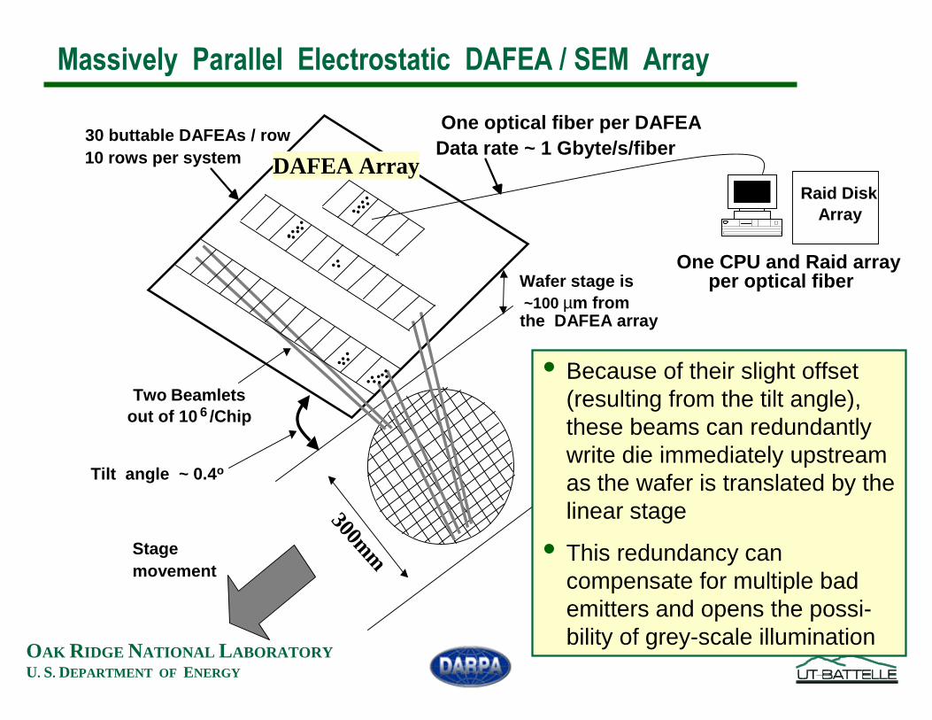
0DVVLYHO\3DUDOOHO(OHFWURVWDWLF'$)($6(0$UUD\
Raid DiskArray
One optical fiber per DAFEAData rate ~ 1 Gbyte/s/fiber
30 buttable DAFEAs / row 10 rows per system
Stage movement
300mm
Wafer stage is~100 µm fromthe DAFEA array
DAFEA Array
Two Beamletsout of 10 6 /Chip
Tilt angle ~ 0.4o
One CPU and Raid arrayper optical fiber
..... ....
...
.....
......
........ • Because of their slight offset (resulting from the tilt angle), these beams can redundantly write die immediately upstream as the wafer is translated by the linear stage
• This redundancy can compensate for multiple bad emitters and opens the possi-bility of grey-scale illumination

OAK RIDGE NATIONAL LABORATORYU. S. DEPARTMENT OF ENERGY
([DPSOH&RPSXWHU*HQHUDWHG'$)($([WUDFWLRQ$FFHOHUDWLRQDQG)RFXVLQJ2SWLFV'HVLJQIRUQP'LDPHWHU3RLQW6RXUFH
The LMCD circuitry beneath each emitter is not shown, nor is the split-ring detector at the top of each focusing stack (to implement the in situ SEM function)
Proposed CNF point-source emitter looks entirely feasible

OAK RIDGE NATIONAL LABORATORYU. S. DEPARTMENT OF ENERGY
• 1RVSDFHFKDUJHOLPLWDWLRQ EHFDXVHRIVPDOOFXUUHQWaQ$− (PLWWHUEHDPVGRQRW´EORZXSµRYHUPOHQJWK− 2QDYHUDJHOHVVWKDQRQHHOHFWURQ LQEHDPSDWKDWDQ\WLPH
• /RWVRI´RYHUKHDGµ IRUPRGLI\LQJH[SRVXUHFRQGLWLRQV− $VVXPHGRSHUDWLQJFRQGLWLRQV
VHFLOOXPLQDWLRQ#.+]RQO\GXW\F\FOHDQG Q$
• 7LPHDYJFXUUHQWa$SHUFP '$)($FKLSa[ HPLWWHUV− FKLSDUUD\SURGXFHVaP$WLPHDYHUDJH− a;6&$/3(/⇒ FRPSDUDEOHLQFUHDVH LQWKURXJKSXW"
• 'HVLJQ&DOFXODWLRQV− (OHFWULFILHOGVWUHQJWKOLPLWHGE\GLHOHFWULFEUHDNGRZQWR9P− )RFXVHGHOHFWURQEHDPOHWVSRWVL]HVRIQPWRQP DW:' P
QPWRQPIHDWXUHVL]HV
• :ULWHZLWKQRPLQDOHOHFWURQEHDPOHWHQHUJ\RI²H9HOLPLQDWLQJWKHSUR[LPLW\HIIHFW
,PSRUWDQW)HDWXUHV'HVLJQ&DOFXODWLRQVIRU(OHFWURVWDWLF2SWLFV(OHFWURQ%HDPOHW ([WUDFWLRQ$FFHOHUDWLRQDQG)RFXVLQJ

OAK RIDGE NATIONAL LABORATORYU. S. DEPARTMENT OF ENERGY
5HFHQW$FFRPSOLVKPHQWVLQ)LHOG(PLWWHU$UUD\'HYHORSPHQW
Key Research Objective for the DEAL ConceptA reliable, stable solid-state emitter, lithographically
placed at each site of a massively parallel array
• Deterministic growth of individual vertically aligned carbon nanofibers (VACNFs) in arrays
• VACNF field emission (FE) measurements and modeling (Part 1)
• Fabrication of gated electrode (diode and triode) structures
• Growth of single VACNFs centered in electrode wells
• First demonstration of gated control of FE from VACNF emitters
• Shape control of VACNF emitters to tailor FE characteristics

OAK RIDGE NATIONAL LABORATORYU. S. DEPARTMENT OF ENERGY
5 µm
+LJKO\'HWHUPLQLVWLF*URZWKRI,QGLYLGXDO9$&1)V+DV%HHQ$FKLHYHGDQG8VHGIRU$UUD\)DEULFDWLRQ
VACNF Growth Is Deterministic
• Catalyst dot pattern: VACNF location
• Nanodroplet size: VACNF tip diam
• Growth time: VACNF height

OAK RIDGE NATIONAL LABORATORYU. S. DEPARTMENT OF ENERGY
Two Critical Tests• Amount of misalignment between
EBL and PL steps
• RIE must uncover Ni dots, to catalyze VACNF growth
([FHOOHQW$OLJQPHQW$FKLHYHG%HWZHHQ(%/DQG3/6WHSV1L'RWV$UH&HQWHUHGLQ(OHFWURGH$SHUWXUHV
Results
• Measurements made after calibrating SEM to 300-nm periodic grating
• Typical misalignment < 50 nm (< 5% of aperture diameter) averaged over ~ 50 devices
• Misalignment of EBL and PL steps is no longer an issue
• A self-aligned process is not needed

OAK RIDGE NATIONAL LABORATORYU. S. DEPARTMENT OF ENERGY
*URZWKRI9HUWLFDOO\$OLJQHG&DUERQ1DQRILEHUV9$&1)V&HQWHUHGLQ(OHFWURGH6WUXFWXUH:HOOV
Proof that
• Two lithography steps placed Ni catalyst dot near center of the aperture
• RIE released Ni dot from PECVD oxide, to catalyze growth of a single, isolated carbon nanofiber
h ~ 950 nmr QP
Both critical tests are met
9$&1)

OAK RIDGE NATIONAL LABORATORYU. S. DEPARTMENT OF ENERGY
3RVW(WFK,PDJHRI7ULRGH6WUXFWXUH
Best-case alignment shown, overlay < 50 nmWorst case observed ~ 100 nm
Ni catalyst dot
Lower gate
Upper gate

OAK RIDGE NATIONAL LABORATORYU. S. DEPARTMENT OF ENERGY
)LUVW'HPRQVWUDWLRQRI&RQWUROOHG)LHOG(PLVVLRQIURPD 0LFURIDEULFDWHG *DWHG$UUD\RI9$&1)(PLWWHUV
• Three SMUs: Independently monitor gate and anode currents • Anode: 700 µm from gate and at +100 volts ( collect FE current)• Gate grounded, cathode swept 0 to –100 volts ( control FE current)• VACNF in 2-µm diam x 1.5-µm deep electrode well:
− Turn-on electric field (1 nA current) = 80 V/µm ( –85 V cathode )
Reproducible, gated control of field emissionfrom a vertically aligned carbon nanofiber emitter

OAK RIDGE NATIONAL LABORATORYU. S. DEPARTMENT OF ENERGY
)LUVW'HPRQVWUDWLRQRI&RQWUROODEOH)LHOG(PLVVLRQIURPD 0LFURIDEULFDWHG *DWHG$UUD\RI9$&1)(PLWWHUVFRQW·G
Reduced FE Turn-On Field and Fowler-Nordheim Behavior
After Initial Operation
• Measure FE I-V after 20 minutes constant-bias testing, with 22 MΩseries ballast resistor
• Turn-on field (1 nA emission) decreases to 60 V/µm
• Fowler-Nordheim plot shows straight-line behavior expected for field-emitted electrons
• More than 99% of field-emitted current goes to anode, less than 1% to gate

OAK RIDGE NATIONAL LABORATORYU. S. DEPARTMENT OF ENERGY
&RQWUROOLQJWKH6KDSHRI1DQRVWUXFWXUHVLQD/DUJH6FDOH6\QWKHVLV3URFHVV
• Dynamically changegrowth conditions to produce cylinder-on-cone geometry
• Cone: Mechanically robust base
• Cylinder: Narrow tip for field emission
• Permits controlling aspect ratio (height / tip radius), to optimize shape for field emission
Growth of Cylinder-on-Cone VACNFs

OAK RIDGE NATIONAL LABORATORYU. S. DEPARTMENT OF ENERGY
&XUUHQWDQG1HDU²)XWXUH5'
• Electrical (turn-on field, stability, lifetime) / structural / compositionalcharacterization to determine and optimize FE from VACNFs. Determine optimum growth conditions for FE.
• Reduce height ( h ) and tip radius ( r ) of VACNFs while maintaining or increasing aspect ratio ( h / r ).
• Develop experimental facilities: (1) wafer-scale growth; (2) rapid, simultaneous FE measurements for VACNF arrays
• Continue developing lithography and processing to fabricate higher aspect ratio and more complex electrode structures.
• Seek industrial partners− Leverage ORNL research capabilities− Move toward prototype DAFEA chips and a tool

OAK RIDGE NATIONAL LABORATORYU. S. DEPARTMENT OF ENERGY
6XPPDU\)LHOG(PLWWHU$UUD\'HYHORSPHQW
• Highly deterministic (catalytically controlled) growth of large arrays of individual vertically aligned carbon nanofibers (VACNFs)
• FE measurements for VACNFs are in reasonable agreement with Fowler-Nordheim modeling
• Fabrication of gated electrode (diode and triode) structures
• VACNFs centered in electrode wells
• Reproducible, controlled FE from gated arrays of VACNF emitters
• VACNF emitters’ shape can be controlled and tailored for FE
• VACNFs are robust to processing steps and promising as field emitters

OAK RIDGE NATIONAL LABORATORYU. S. DEPARTMENT OF ENERGY
'($/6XPPDU\
• A massively parallel, maskless, direct-write Digital E-beam Array Lithography (DEAL) system appears feasible
• Large areas may be written on wafers with multiple Digitally Addressable Field Emitter Array (DAFEA) chips
• Design tradeoffs permit scaling at 60 WPH from 40-nm features/linewidths down to 10-nm features/linewidths
• Industrial partners (a DAFEA chip fabrication partner and a tool partner) are needed now to transform this R&D effort into a prototype tool

OAK RIDGE NATIONAL LABORATORYU. S. DEPARTMENT OF ENERGY
$FNQRZOHGJPHQWV
• DARPA Advanced Lithography Program (Dr. David O. Patterson)
• Cornell Nanofabrication Facility
• Professor David Joy (U. Of Tennessee / ORNL)
• ORNL Laboratory Directed R&D Fund (initial support)
ORNL is managed by UT-Battelle, LLC, for the U. S. Department of Energy under contract No. DE-AC05-00OR22725

OAK RIDGE NATIONAL LABORATORYU. S. DEPARTMENT OF ENERGY
(OHFWURQ6RXUFH7HFKQRORJ\DQG0DVVLYHO\3DUDOOHO'LJLWDO(OHFWURVWDWLF(%HDP$UUD\
/LWKRJUDSK\'($/
'+/RZQGHV /5%D\ORU ('(OOLV 0$*XLOORUQ $0HOHFKNR
9,0HUNXORY 0/6LPSVRQ -+:KHDOWRQ -%:LOJHQ
-(+DUG\ '3+XWFKLQVRQ
6ROLG6WDWH'LYLVLRQ ,QVWUXPHQWDWLRQDQG&RQWUROV'LYLVLRQ )XVLRQ(QHUJ\'LYLVLRQ (QJLQHHULQJ7HFKQRORJ\'LYLVLRQ
2DN5LGJH1DWLRQDO/DERUDWRU\ 'HSDUWPHQWRI(OHFWULFDO(QJLQHHULQJ8QLYHUVLW\RI7HQQHVVHH
&RUUHVSRQGHQFH
ORZQGHVGK#RUQOJRYED\ORUOU#RUQOJRYKXWFKLQVRQGS#RUQOJRY

OAK RIDGE NATIONAL LABORATORYU. S. DEPARTMENT OF ENERGY
287/,1( (OHFWURQVRXUFHWHFKQRORJLHV '($/&RQFHSWDQG&DSDELOLWLHV
± 'LJLWDOO\$GGUHVVDEOH)LHOG(PLWWHU$UUD\'$)($FRQFHSW± 2QFKLSHOHFWURVWDWLFOHQVFRQFHSW
&XUUHQW5HVHDUFK2EMHFWLYHVDQG$SSURDFK
5HFHQW$FFRPSOLVKPHQWVLQ)LHOG(PLWWHU$UUD\'HYHORSPHQW± 'HWHUPLQLVWLFJURZWKRILQGLYLGXDOYHUWLFDOO\DOLJQHGFDUERQ
QDQRILEHUV9$&1)VLQDUUD\V± 9$&1)ILHOGHPLVVLRQ)(SURSHUWLHVDQGPRGHOLQJ± )DEULFDWLRQRIJDWHGHOHFWURGHGLRGHDQGWULRGHVWUXFWXUHV± *URZWKRIVLQJOH9$&1)VFHQWHUHGLQHOHFWURGHZHOOV± 6KDSHFRQWUROIRU9$&1)HPLWWHUV± $GYDQWDJHVDQGIHDVLELOLW\RIJURZLQJWKH9$&1)DUUD\ILUVW
3ODQVIRU)XWXUH'HYHORSPHQW

OAK RIDGE NATIONAL LABORATORYU. S. DEPARTMENT OF ENERGY
%ULJKWQHVV KLJKEULJKWQHVVQHHGHG![ $FPVU#N9GRVHRIµ&FPUHTXLUHG
/RZHQHUJ\VSUHDG± WRPLQLPL]HVRXUFHGLYHUJHQFHQHHGH9
6WDELOLW\± YDULDWLRQRYHUDKUSHULRGGHVLUDEOH
/LIHWLPH a\UIRUDQHFRQRPLFOLWKRJUDSK\WRRO
8QLIRUPLW\ YDULDWLRQVRIDIHZLQEULJKWQHVVEHWZHHQPXOWLD[LV VRXUFHV
0RGXODWLRQ± VZLWFKLQJWLPHVRIµVQHHGHGIRUKLJKWKURXJKSXWFDSDELOLW\
(OHFWURQ%HDP6RXUFH5HTXLUHPHQWVIRU0DVNOHVV/LWKRJUDSK\

OAK RIDGE NATIONAL LABORATORYU. S. DEPARTMENT OF ENERGY
(OHFWURQ%HDP6RXUFHVIRU0DVNOHVV/LWKRJUDSK\
NEAPhotocathode
ν
e- e-+V
AmorphousDiamond (aD, DLC)Field Emitters
CarbonNanotube/fiber(CNT,CNF) Φ ~ 4eVField Emitters
e-+V
e-
ThermionicLaB6 W &ROG&DWKRGH)LHOG(PLWWHUV
e-
SchottkyW Zr
Spindt tips0R 6L
e-
+V
$YDULHW\RIHOHFWURQVRXUFHWHFKQRORJLHVKDYHEHHQH[DPLQHGIRUPDVNOHVVOLWKRJUDSK\

OAK RIDGE NATIONAL LABORATORYU. S. DEPARTMENT OF ENERGY
3KRWRFDWKRGH6RXUFHV
3ULQFLSOHRIRSHUDWLRQ²± 3KRWRQVIURPDODVHUDUHLQFLGHQWRQDWKLQILOPFDXVLQJ
HOHFWURQVWREHHPLWWHGZLWK(P Kν Φ
3URSHUWLHV± 0DWHULDOV*D$V *D$V3*D1$X&V2DFWLYDWLRQXVHG
IRUQHJDWLYHHOHFWURQDIILQLW\1($
± 4XDQWXPHIILFLHQF\GHWHUPLQHVEULJKWQHVVFHVLDWHG*D1IRULQVWDQFHFDQEHa
± /RZHQHUJ\VSUHDGH9
&XUUHQWUHVHDUFK²
± 2YHUFRPH&VGHSOHWLRQDQGWUDSSHGHOHFWURQV
± *D1ORRNVSURPLVLQJ0DFKXFDHWDO-967%
5HVHDUFKJURXSV6WDQIRUG8QLY,QWHYDF2*,(WHF« 2WKHUDSSOLFDWLRQVLQWHQVLILHUVQLJKWYLVLRQDFFHOHUDWRU
VRXUFHVDVWURSK\VLFVGHWHFWRUV (QRXJKSDUDOOHOVRXUFHVIRUKLJKWKURXJKSXWPDVNOHVV(%/"
NEAPhotocathode
ν
e-

OAK RIDGE NATIONAL LABORATORYU. S. DEPARTMENT OF ENERGY
6FKRWWN\)LHOG(PLWWHUV
3ULQFLSOHRIRSHUDWLRQ²± (OHFWURQVDUHHPLWWHGIURPWKHWLSGXHWRERWKWKHUPDO
H[FLWDWLRQDQGWKHHOHFWULFILHOGIURPDQH[WUDFWRUHOHFWURGH
3URSHUWLHV± 3UHGRPLQDQWHOHFWURQVRXUFHWHFKQRORJ\
± 0DWHULDOV7XQJVWHQZLUHKHDWHGWR.
± +LJKEULJKWQHVV
OAK RIDGE NATIONAL LABORATORYU. S. DEPARTMENT OF ENERGY
7KHUPLRQLF (PLWWHUV
e-
ThermionicLaB6 W
3ULQFLSOHRIRSHUDWLRQ ±± (OHFWURQVDUH´ERLOHGRIIµRIKHDWHGHPLWWHU
3URSHUWLHV± 0DWXUHHOHFWURQVRXUFHWHFKQRORJ\
± 0DWHULDOV7XQJVWHQ/D%!.
± +LJKVWDELOLW\DQGORZWKHUPDOQRLVH
± a506FXUUHQWVWDELOLW\
± 0RGHUDWHEULJKWQHVVa[ $FPVUN9
± 6HUYLFHOLIHaK
2WKHUDSSOLFDWLRQV9DFXXPWXEHV&57V« (QRXJKSDUDOOHOVRXUFHVIRUKLJKWKURXJKSXWPDVNOHVV
(%/"± aWLPHVODUJHUWKDQ6FKRWWN\HPLWWHUVRUFROG
FDWKRGHV

OAK RIDGE NATIONAL LABORATORYU. S. DEPARTMENT OF ENERGY
6SLQGW 7LS)LHOG(PLWWHUV
&ROGFDWKRGHSULQFLSOHRIRSHUDWLRQ ±± (OHFWURQVWXQQHOWKURXJKVXUIDFHSRWHQWLDO
EDUULHUZLWKVWURQJDSSOLHGHOHFWULFILHOG
6SLQGWWLSHPLWWHUVGHYHORSHGIRUPLQLDWXUHSDUDOOHODUUD\V
± 6SLQGWHWDO- $SSO3K\V
3URSHUWLHV± 0DWHULDOV0R6L
± *RRGSHUIRUPDQFHLQ8+9
± /DUJHVFDOHIDEULFDWLRQLVSRVVLEOH
3RRUHQYLURQPHQWDOVWDELOLW\± 5HFHQWH[DPSOHVKRUWOLIHWLPHRI0RWRUROD·V
ILHOGHPLVVLRQGLVSOD\EDVHGRQ0RILHOGHPLWWHUV
Spindt tips0R 6L
e-
+V

OAK RIDGE NATIONAL LABORATORYU. S. DEPARTMENT OF ENERGY
6LOLFRQ)LHOG(PLWWHUV)DEULFDWLRQ3HUIRUPDQFH
9DULDWLRQRI6SLQGW WLSXVLQJ6L
± 8WLOL]HVVWDQGDUGVHPLFRQGXFWRUSURFHVVLQJ
*RRGSHUIRUPDQFHLQ8+9
Temple et al., J. Vac. Sci. Technol. A 16, 1980 (1998)
P ~ 10-9 Torr

OAK RIDGE NATIONAL LABORATORYU. S. DEPARTMENT OF ENERGY
6SLQGW7LS)LHOG(PLWWHUV6XPPDU\
+LJKOHYHORILQWHJUDWLRQ
+LJKFXUUHQWGHQVLWLHV
/RZSRZHUFRQVXPSWLRQ
3RRUHQYLURQPHQWDOVWDELOLW\ RI6LDQG0RWLSVGXHWRLRQERPEDUGPHQWDQGVXUIDFHFKHPLVWU\R[LGHIRUPDWLRQDGVRUEDWHV
Spindt tips0R 6L
e-
+V
6LWLSH[SRVXUHWR2

OAK RIDGE NATIONAL LABORATORYU. S. DEPARTMENT OF ENERGY
&DUERQ)LEHU)LHOG(PLWWHUV
&DUERQILEHUVKDYHEHHQH[DPLQHGIRUFROGFDWKRGH)(DSSOLFDWLRQVIRUPRUHWKDQ\UV
([FHOOHQWHQYLURQPHQWDOVWDELOLW\DQGOLIHWLPH
– Baker et al., J. Phys. D 7, 2105 (1974)
P ~ 1 x 10⁻⁶ Torr
RT
1100 K
RT100 MOhm

OAK RIDGE NATIONAL LABORATORYU. S. DEPARTMENT OF ENERGY
&DUERQ1DQRWXEH&17)LHOG(PLWWHUV
0RUHUHFHQWO\FDUERQQDQRWXEHVDQGQDQRILEHUVKDYHEHHQH[DPLQHGIRUFROGFDWKRGH)(DSSOLFDWLRQV
9HU\SURPLVLQJ)(SURSHUWLHV– Choi et al., , Appl. Phys. Lett. 75,
3129 (1999)
Nanotube Emitters

OAK RIDGE NATIONAL LABORATORYU. S. DEPARTMENT OF ENERGY
)LHOG(PLVVLRQ'LVSOD\ZLWK&17EDVHG&DWKRGHV6DPVXQJ
5HVLVWDQFHWRVSXWWHULQJDQGFKHPLFDOLQHUWQHVVRIFDUERQ([FHOOHQWHQYLURQPHQWDOVWDELOLW\
+LJKDVSHFWUDWLRRI&17V /RZ)(WXUQRQILHOG
3UREOHP PXOWLSOHHPLWWLQJVLWHVLQHDFKFDWKRGH !GLIILFXOWWRSURGXFHDZHOOIRFXVHGHOHFWURQEHDP

OAK RIDGE NATIONAL LABORATORYU. S. DEPARTMENT OF ENERGY
9HUWLFDOO\$OLJQHG&DUERQ1DQRILEHUV9$&1)V
9$&1)VKDYHEHHQGHYHORSHGLQDQDWWHPSWWRSURGXFHWKHLGHDOILHOGHPLWWHU
± 5HVHPEOHPXOWLZDOOHG&17VEXWVPDOOHUJUDLQVL]HVGXHWRORZHUWHPSHUDWXUHJURZWK
'HWHUPLQLVWLFJURZWKRI9$&1)VIDEULFDWLRQRIKLJKO\LQWHJUDWHGJDWHGFDWKRGHVWUXFWXUHVLVSRVVLEOH
6LQJOH9$&1)WLSSHUFDWKRGHDZHOOIRFXVHGHOHFWURQEHDPFDQEHSURGXFHG
+LJKDVSHFWUDWLRRI9$&1)V ORZ)(WXUQRQILHOG
5HVLVWDQFHWRVSXWWHULQJDQGFKHPLFDOLQHUWQHVVRIFDUERQ ORQJOLIHWLPH
CarbonNanotube/fiber(CNT,CNF) Φ ~ 4eVField Emitters
e-+V
[ Merkulov, Lowndes, Wei, and Eres,Appl. Phys. Lett. 76, 3555 (2000) ]

OAK RIDGE NATIONAL LABORATORYU. S. DEPARTMENT OF ENERGY
7KHHOHFWULFILHOGDWDVKDUSWLSRQDVKDQN LVJLYHQE\Elocal ~ ( h / r ) Eapplied ~ β Eapplied
ZKHUH(ORFDO WLS HOHFWULFILHOG (DSSOLHG DSSOLHGYROWDJHGLVWDQFHK KHLJKWRIWKHVKDQN U WLSUDGLXV
)RUQPWLSGLDPHWHU &1)VWKLVLPSOLHVHPLVVLRQDWa9PVFDOLQJIURP9PIRUQPWLSGLDPHWHULIK FRQVWDQW
$YROWJULGSRWHQWLDODWQPVHSDUDWLRQGULYHQE\ &026FLUFXLWU\ZRXOGFRQWUROVXFKD9$&1)HPLWWHU
)LHOG(PLVVLRQDVD)XQFWLRQRI&DUERQ1DQRILEHU$VSHFW5DWLRKU

OAK RIDGE NATIONAL LABORATORYU. S. DEPARTMENT OF ENERGY
r/h
0.000 0.002 0.004 0.006
Eto
(V
/µm
)
0
10
20
30
40
50
60
70VACNFVACNF + RIE
E (V/µm)
20 22 24 26 28 300.0
0.5
1.0
1.5
2.0
2.5
1/E
0.030 0.035 0.040 0.045 0.050-28
-26
-24
-22
-20
-18
I (10
-6A
)
l n( I
/ E2 )
E (V/µm)
20 22 24 26 28 300.0
0.5
1.0
1.5
2.0
2.5
1/E
0.030 0.035 0.040 0.045 0.050-28
-26
-24
-22
-20
-18
I (10
-6A
)
l n( I
/ E2 )
)LHOG(PLVVLRQ0HDVXUHPHQWVRI,VRODWHG9$&1)V5HYHDO([SHFWHG(PLVVLRQ&KDUDFWHULVWLFV
$QDO\VHVRI,²9FKDUDFWHULVWLFVLPSO\D)RZOHU1RUGKHLPOLNHWXQQHOLQJHPLVVLRQPHFKDQLVP
(PLVVLRQWXUQRQILHOGVa9P∝ UKDVH[SHFWHG± 6OLJKWO\KLJKHUWKDQH[SHFWHGIURP)RZOHUB1RUGKHLPWKHRU\DVVXPLQJ
HPLVVLRQIURPHQWLUHWLSUDGLXV± 9$&1)VH[SRVHGWRUHDFWLYHLRQHWFK5,(KDYHORZHUHGHPLVVLRQWKUHVKROG

OAK RIDGE NATIONAL LABORATORYU. S. DEPARTMENT OF ENERGY
Time (hrs)
0 5 10 15 20
E_t
o (V
/µm
)0
5
10
15
20
25
30
35
40
/LIHWLPH6WDEOH&:ILHOGHPLVVLRQRSHUDWLRQDWQ$PHDVXUHGIRU!KRXUVIRULVRODWHG251/9$&1)V
± 7KUHVKROGFKDQJHVVKRZQLQSORWIRUKUV± -DSDQHVHJURXS>$3/@
KRXUV&:ZLWK0:&17V
,QWULQVLF HQYLURQPHQWDOVWDELOLW\RI)(IURPFDUERQQDQRWXEHHPLWWHUV
>.$'HDQ%5&KDODPDOD0RWRUROD$3/DQG$3/@
± 6:17VPXFKOHVVVHQVLWLYHWRHQYLURQPHQWWKDQPHWDOOLFHPLWWHUV
± 1RFXUUHQWUXQDZD\DUFLQJ8QEDOODVWHGRSHUDWLRQ
± 6WDELOLW\/RZVSXWWHU\LHOGORZ&DWRPPRELOLW\VWURQJERQGLQJ
/LIHWLPHRI)LHOG(PLVVLRQIURP,VRODWHG9$&1)V

OAK RIDGE NATIONAL LABORATORYU. S. DEPARTMENT OF ENERGY
(OHFWURQ6RXUFHV 6XPPDU\
&RQYHQWLRQDOVRXUFHWHFKQRORJLHVKDYHSURPLVLQJFKDUDFWHULVWLFVIRUPDVNOHVVOLWKRJUDSK\DSSOLFDWLRQV
± ,QSDUWLFXODUSKRWRFDWKRGHVDQG6FKRWWN\HPLWWHUVORRNDWWUDFWLYH
± &DQWKHVHVRXUFHVEHFRQILJXUHGWRSURGXFHHQRXJKSDUDOOHOEHDPVWRPDNHPDVNOHVVOLWKRJUDSK\DWWUDFWLYH"
1HZHUFDUERQQDQRWXEHEDVHGILHOGHPLWWHUVDUHVWDUWLQJWRORRNDWWUDFWLYHIRUPDVVLYHSDUDOOHODSSOLFDWLRQV
± 6WD\WXQHGDVWKLVWHFKQRORJ\GHYHORSV

KPS 010828 1
Keith Standiford, Consulting Services
Maskless Lithography Data Issues:
What’s in a Mask?

KPS 010828 2
Keith Standiford, Consulting Services
The Mask is a Data Storage Device
• Storage capacity
• Transfer rate
• Physical representation transformation
• Physical size constraints
• Reliability (Data Integrity)
⇔MASK

KPS 010828 3
Keith Standiford, Consulting Services
What is the pixel size?
W The pixel size is NOT the MFS
W It is also probably not a “rule” based on MFS
A rule based on CD control required
MFS (minimum feature size)± CD Control
AU (address unit) for edge placement

KPS 010828 4
Keith Standiford, Consulting Services
Mask Storage Capacity
Assume:6.25 square cm chips AU = 1/2 CD control tolerance
10
100
1000
050100150200
Tera-pixels per Mask
Roadmap Node
We need Data Compression!
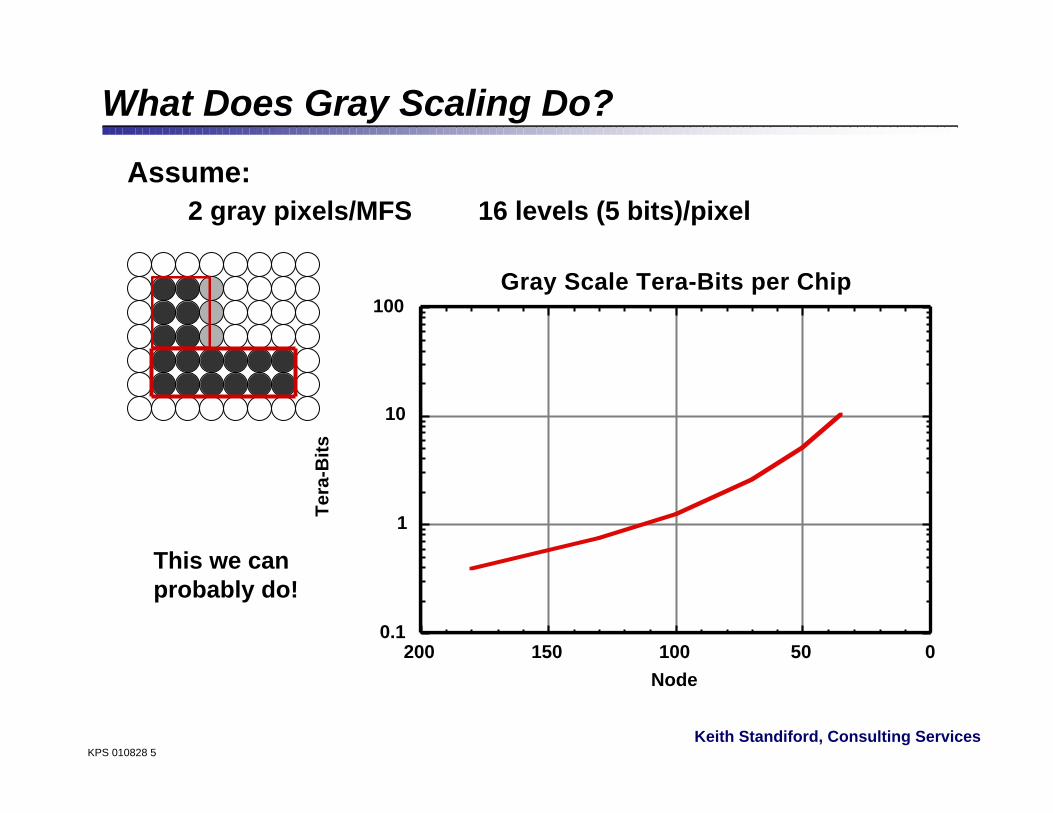
KPS 010828 5
Keith Standiford, Consulting Services
What Does Gray Scaling Do?
Assume:2 gray pixels/MFS 16 levels (5 bits)/pixel
This we canprobably do!
0.1
1
10
100
050100150200
Gray Scale Tera-Bits per Chip
Ter
a-B
its
Node

KPS 010828 6
Keith Standiford, Consulting Services
Transfer Rate – Throughput Requirements
Assume:300 mm wafers 30 seconds “beam-on” time
10
100
1000
10 4
050100150200
AU-based Tera-Pixels/sec
Node
We (still) need Data Compression!

KPS 010828 7
Keith Standiford, Consulting Services
Try Gray Scaling Again
Assume:2 gray pixels/MFS 16 levels (5 bits)/pixel
This beginsto make menervous!
1
10
100
050100150200
Gray Scale Tera-Bits/sec
Node

KPS 010828 8
Keith Standiford, Consulting Services
Can We Get 5 Tb/sec of Data?
• Current B/W- 25 Gb/sec (Rambus)
- 20 “systems”/Tb/sec –– 100 “systems” for 5 Tb/sec
- May be do-able
• Data compression- Loss-less methods
- 10 – 100 fold compression reported
- 2 – 20 systems for 5 Tb/sec
- This we could do
• Data transmission- 5 – 50 channels at 10 Gb/sec
- This we could also do

KPS 010828 9
Keith Standiford, Consulting Services
Clock Rate – an aside …
Gray Pixel Rate = number of beams X beam clock rate
0.1
1
10
050100150200
Gray Tera-Pixels/sec
Node

KPS 010828 10
Keith Standiford, Consulting Services
Physical Representation Transformation
• Data must be transformed from its form of physicalstorage to some representation which will alter thephysical properties of the wafer in order to affect thepattern transfer for lithography.
• Masks:- Data stored as clear/opaque spots (or scattering, phase
shifting, reflecting, etc.)
- Transformed to presence or absence (or interference) ofradiation at the wafer
• Mask-less:- Electronic data storage and transmission
- Transformed to (insert method here) at “print head”
What?!?

KPS 010828 11
Keith Standiford, Consulting Services
Physical Size Constraints
• Masks are “about the same size” as wafers- Imaging physics
- Fabrication practicalities
• Mask-less size varies with printing physics- Chip Scale methods – 1X printers
• Ink jets
• Nano-probes
- Wafer scale methods
• Stripe , sub-field or chip printing reduction methods
• Micro-columns
• Hybrids – multiple “chip scale” copies

KPS 010828 12
Keith Standiford, Consulting Services
Required Functionality
• Receive compressed data
• Expand compressed data
• Implement gray scales- DAC, pulse width modulation, etc.
• Implement the “actuator”
• “Drive” the “actuator”- Blanker, mechanical deflector, etc.
- Deflection drives, source power, etc.
• Connect to the “actuator”- N wires per channel
⇒ It all has to fit in the available space!

KPS 010828 13
Keith Standiford, Consulting Services
Wafer Scale Space Budget
In a 300 mm diameter, how much space can we afford?
1
10
100
1000
050100150200
Square mm/Function/second(Wafer Scale)
Giga-Pixel/sec (Wafer Scale)Giga-bit/sec (Wafer Scale)
Sq
uar
e m
m.
Node
Remember:EVERYTHINGhas to fit. This isactually hard!

KPS 010828 14
Keith Standiford, Consulting Services
Chip Scale Space Budget
In a square 25 on a side, how much space can we afford?
Remember:EVERYTHINGstill has to fit.This is evenharder!
0.01
0.1
1
10
050100150200
Square mm/Function/second(Chip Scale)
Giga-Pixel/sec (Chip Scale)Giga-bit/sec (Chip Scale)
Sq
uar
e m
m.
Node

KPS 010828 15
Keith Standiford, Consulting Services
Reliability (Data Integrity) for Masks
• Characterize data storage accuracy- CD measurements
- Overlay measurements
- Defect inspection/repair
- Yield characterization
• Monitor and preserve integrity- Pellicles
- Periodic re-inspection
⇒ Masks are quite “non-volatile” storage!
Masks are not really very accurate!

KPS 010828 16
Keith Standiford, Consulting Services
Mask-less Accuracy and Integrity
• Variations in:- placement
- delivered “dose”
- etc.
• Functionality- do they all actually work?
• Usual solution is redundancy- Average out the errors
- A strategy for “dead pixels”
• Average them out
• Overlap to write them with a good one
• Note: Stuck “ON” is harder to overcome!
Mostly thought of as “actuator” issues:

KPS 010828 17
Keith Standiford, Consulting Services
What About DATA Integrity?
• We have Tera-bits of data transmitted and processedfor every wafer.
• We have thousands up to millions of data channels atthe “print head”.
• Data integrity is no longer guaranteed by justpreserving a physical structure.
• Data handling faults can destroy weeks worth of WIPbefore discovered at final probe.
• Why hasn’t this come up with masks?- Number of probes is small enough that intermittent
faults still make lots and lots of errors
- Mask inspection finds most of the errors, eventually!
This question hasn’t been asked much!

KPS 010828 18
Keith Standiford, Consulting Services
Mask-less Lithography Needs Fault Tolerance!
• Manufacturing yield will demand fault detection
• Reliability, maintainability, serviceability demandsfault tolerance
- Uptime requirements
- Overall system complexity
• How far down into the system?- Data transmission
- Data expansion
- Actuator function
• It still has to fit in the available space!
⇒ This is hard, but without it we have a showstopper
MORE than just fault detection…

KPS 010828 19
Keith Standiford, Consulting Services
Summary
• Storage capacity: probably OK
• Transfer rate: probably OK
• Physical representation transformation: technologydependent
• Physical size constraints: looks difficult
• Reliability (Data Integrity): difficult, largely unexplored
We have examined replacing the mask as a data storage device:
⇔MASK

RSM Maskless Litho Workshop Opening remarks 8/28/01 1
Your Job Today...• Listen critically!
– Are the programs tracking the needs of the industry?– Are the program timing and requirements meeting
your expectations?
• Develop opinions
• Constructively feedback in afternoon sessions
– Provide feedback on technology progress– Provide areas of further work (Critical Issues) that
need to be addressed

RSM Maskless Litho Workshop Opening remarks 8/28/01 2
Now our job….• We thank you for participating!
• We will:– Post presentations to SRC/ISMT web– Roll up results and distribute to participants– Develop action plan that responds to your feedback– Continue to monitor programs & determine how/where we can
affect technology development– Continue to include world-wide programs– ISMT/SRC will work together to continue industry involvement
• Reception @ 6:00 in the Horseshoe Garden Terrace

RSM Maskless Litho Workshop Opening remarks 8/28/01 3
The rest of your job….• If you have not already given us a soft copy
of your presentation, please do so by the end of this week.
• Send it in either PowerPoint or Acrobat .pdf format to: [email protected]

2001 Maskless Lithography Critical Issues
• Economic analysis including: CoO, Cycle time, Market segment and application
• Data path/flow issues including compression/decompression and redundancy
• Simultaneous calibration and control of many beams
• Demonstration of working scalable system• Define verification and inspection steps
unique to ML2• Thin resist development (low kV)• Overlay and alignment strategy


