118
DisplayPort 1.4 TX Subsystem v2.1 Product Guide Vivado Design Suite PG299 (v2.1) August 31, 2020

DisplayPort 1.4 TXSubsystem v2.1
Product GuideVivado Design Suite
PG299 (v2.1) August 31, 2020

Table of ContentsChapter 1: Introduction.............................................................................................. 4
Features........................................................................................................................................4IP Facts..........................................................................................................................................5
Chapter 2: Overview......................................................................................................6Unsupported Features................................................................................................................7Licensing and Ordering.............................................................................................................. 8
Chapter 3: Product Specification........................................................................... 9AXI4-Stream Video Interface......................................................................................................9Native Video Interface.............................................................................................................. 10Subsystem Sub-core Descriptions...........................................................................................11Standards................................................................................................................................... 14Resource Use............................................................................................................................. 15Port Descriptions.......................................................................................................................15Register Space........................................................................................................................... 20
Chapter 4: Designing with the Subsystem..................................................... 37DisplayPort Overview................................................................................................................37EDID I2C Speed Control............................................................................................................54eDP Support...............................................................................................................................55Pixel Mapping............................................................................................................................ 55AXI4-Stream Interface Color Mapping ...................................................................................63Clocking...................................................................................................................................... 64Resets..........................................................................................................................................65Address Map Example.............................................................................................................. 65
Chapter 5: Design Flow Steps.................................................................................66Customizing and Generating the Subsystem........................................................................ 66Constraining the Subsystem....................................................................................................68Simulation.................................................................................................................................. 70Synthesis and Implementation................................................................................................70
PG299 (v2.1) August 31, 2020 www.xilinx.comDisplayPort 1.4 TX Subsystem v2.1 2Send Feedback
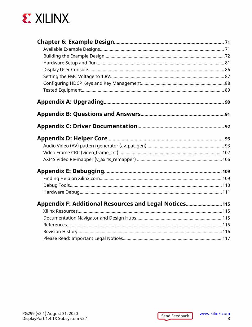
Chapter 6: Example Design..................................................................................... 71Available Example Designs...................................................................................................... 71Building the Example Design...................................................................................................72Hardware Setup and Run......................................................................................................... 81Display User Console................................................................................................................ 86Setting the FMC Voltage to 1.8V.............................................................................................. 87Configuring HDCP Keys and Key Management.....................................................................88Tested Equipment..................................................................................................................... 89
Appendix A: Upgrading............................................................................................. 90
Appendix B: Questions and Answers.................................................................91
Appendix C: Driver Documentation................................................................... 92
Appendix D: Helper Core.......................................................................................... 93Audio Video (AV) pattern generator (av_pat_gen) ............................................................... 93Video Frame CRC (video_frame_crc)..................................................................................... 102AXI4S Video Re-mapper (v_axi4s_remapper) ......................................................................106
Appendix E: Debugging........................................................................................... 109Finding Help on Xilinx.com.................................................................................................... 109Debug Tools............................................................................................................................. 110Hardware Debug..................................................................................................................... 111
Appendix F: Additional Resources and Legal Notices............................115Xilinx Resources.......................................................................................................................115Documentation Navigator and Design Hubs...................................................................... 115References................................................................................................................................115Revision History.......................................................................................................................116Please Read: Important Legal Notices................................................................................. 117
PG299 (v2.1) August 31, 2020 www.xilinx.comDisplayPort 1.4 TX Subsystem v2.1 3Send Feedback

Chapter 1
IntroductionThe Xilinx® DisplayPort 1.4 TX Subsystem implements the functionality of a video source asdefined by the Video Electronics Standards Association (VESA) DisplayPort standard v1.4 andsupports driving resolutions of up to Full Ultra HD (FUHD) 8K at 30 fps. The Xilinx DisplayPortsubsystem provides highly integrated IP blocks requiring very little customization.
Features• Support for DisplayPort Source (TX) transmissions
• Supports multi-stream transport (MST) and single stream transport (SST)
• Dynamic lane support (1, 2, or 4 lanes)
• Dynamic link rate support (1.62/2.7/5.4/8.1 Gb/s)
• Dynamic support for 6, 8, 10, 12, or 16 bits per component (BPC)
• Dynamic support for RGB/YCbCr444/YCbCr422 color formats
• Supports 16-bit Video PHY (GT) interface
• Supports 2 to 8 channel audio with 44/48 kHz sample rates
• Supports HDCP 1.3 and HDCP 2.2 encryption in SST
• Supports native or AXI4-Stream video input interface
• Pixel mode support in native video interface mode
• Supports Linear PCM 2-channel audio format
• Supports single audio stream in MST mode
• Supports SDP packet for static HDR mode
• Supports eDP v1.4b
Chapter 1: Introduction
PG299 (v2.1) August 31, 2020 www.xilinx.comDisplayPort 1.4 TX Subsystem v2.1 4Send Feedback

IP FactsSubsystem IP Facts Table
Subsystem Specifics
Supported Device Family1 UltraScale+™ Families (GTHE4, GTYE4)UltraScale™ Families (GTHE3)Zynq® UltraScale+™ RFSoC (GTYE4)
Supported User Interfaces AXI4-Stream, AXI4-Lite, Native video
Resources Performance and Resource Use web page
Provided with Subsystem
Design Files Hierarchical subsystem packaged with DisplayPort TX core and other IP cores
Example Design Vivado® IP integrator
Test Bench Not Provided
Constraints File IP cores delivered with XDC files
Simulation Model Not Provided
Supported S/W Driver Standalone, Linux2
Tested Design Flows3
Design Entry Vivado Design Suite
Simulation For supported simulators, see the Xilinx Design Tools: Release Notes Guide.
Synthesis Vivado Synthesis
Support
Release Notes and Known Issues Master Answer Record: 70295
All Vivado IP Change Logs Master Vivado IP Change Logs: 72775
Xilinx Support web page
Notes:1. For a complete list of supported devices, see the Vivado IP catalog.2. (<install_directory>/Vitis/<release>/data/embeddedsw/doc/xilinx_drivers.htm). Linux OS and
driver support information is available from the Xilinx Wiki page.3. For the supported versions of third-party tools, see the Xilinx Design Tools: Release Notes Guide.
Chapter 1: Introduction
PG299 (v2.1) August 31, 2020 www.xilinx.comDisplayPort 1.4 TX Subsystem v2.1 5Send Feedback

Chapter 2
OverviewThe DisplayPort 1.4 TX Subsystem is a feature-rich, hierarchically packaged subsystem with aDisplayPort (TX) core ready to use in applications in large video systems.
The DisplayPort 1.4 TX Subsystem, in both AXI4-Stream and native interfaces, operates in thefollowing video modes:
• Single stream transport (SST)
• Multi-stream transport (MST) up to 4 streams
RECOMMENDED: Xilinx® recommends a redriver for the TX subsystem solution.
The following table shows the core support for UltraScale™ and UltraScale+™ families. For moreinformation on the device constraint/dependency, see the Video PHY Controller LogiCORE IPProduct Guide (PG230) and respective device family datasheets. Speed grade and temperatureinformation can be found in the UltraScale Architecture and Product Data Sheet: Overview (DS890)and the Defense-Grade UltraScale Architecture Data Sheet: Overview (DS895).
Table 1: Core Support
Device Family Device Data Sheet Speed GradeWithout MST (or)
Without HDCP1.3/2.2
With MST (or)With HDCP 1.3/2.2
Kintex UltraScale Kintex UltraScale FPGAsData Sheet: DC and ACSwitchingCharacteristics (DS892)
-1 5.4 Gb/s 2.7 Gb/s
-2, -3 8.1 Gb/s 5.4 Gb/s
Virtex UltraScale Virtex UltraScale FPGAsData Sheet: DC and ACSwitchingCharacteristics (DS893)
-1 5.4 Gb/s 2.7 Gb/s
-2, -3 8.1 Gb/s 5.4 Gb/s
Kintex UltraScale+ Kintex UltraScale+FPGAs Data Sheet: DCand AC SwitchingCharacteristics (DS922)
-1LI (VCCINT = 0.72 V) 2.7 Gb/s
-1LI (VCCINT = 0.85 V) 5.4 Gb/s
-2LE (VCCINT = 0.72 V) 5.4 Gb/s
-1, -1E, -1I, -1M, -1Q 5.4 Gb/s
-2, -2E, -2I, -3, -3E 8.1 Gb/s
Chapter 2: Overview
PG299 (v2.1) August 31, 2020 www.xilinx.comDisplayPort 1.4 TX Subsystem v2.1 6Send Feedback

Table 1: Core Support (cont'd)
Device Family Device Data Sheet Speed GradeWithout MST (or)
Without HDCP1.3/2.2
With MST (or)With HDCP 1.3/2.2
Zynq UltraScale+MPSoC
Zynq UltraScale+ MPSoCData Sheet: DC and ACSwitchingCharacteristics (DS925)
-1LI (VCCINT = 0.72 V) 2.7 Gb/s
-1LI (VCCINT = 0.85 V) 5.4 Gb/s
-2LE (VCCINT = 0.72 V) 5.4 Gb/s
-1, -1E, -1I, -1M, -1Q 5.4 Gb/s
-2, -2E, -2I, -3, -3E 8.1 Gb/s
Virtex UltraScale+ Virtex UltraScale+ FPGAData Sheet: DC and ACSwitchingCharacteristics (DS923)
-1 (VCCINT = 0.85 V) 5.4 Gb/s
-2 (VCCINT = 0.72 V) 5.4 Gb/s
-2, -3 8.1 Gb/s
Zynq UltraScale+RFSoC
Zynq UltraScale+ RFSoCData Sheet: DC and ACSwitchingCharacteristics (DS926)
-1LI (VCCINT = 0.72 V) 2.7 Gb/s
-1LI (VCCINT = 0.85 V) 5.4 Gb/s
-1, -1E, -1I, -1M 5.4 Gb/s
-2LE (VCCINT = 0.72 V) 5.4 Gb/s
-1 (VCCINT = 0.72 V) 5.4 Gb/s
-2 (VCCINT = 0.72 V) 5.4 Gb/s
-1 (VCCINT = 0.85 V) 5.4 Gb/s
-2, -2E, -2I 8.1 Gb/s
Unsupported FeaturesThe following features of the standard are not supported in the subsystem:
• In-band stereo
• Video AXI4-Stream interface is not scalable with dynamic pixel mode selection
• Dual-pixel splitter is not supported in native video mode
• HDCP is not supported in MST mode
• iDP
• Global Time Code (GTC)
• Non-LPCM audio
• DSC and/or FEC
• 16/32 channel audio
• Interlaced video in AXI4 Streaming interface
• 420 Colorimetry
Chapter 2: Overview
PG299 (v2.1) August 31, 2020 www.xilinx.comDisplayPort 1.4 TX Subsystem v2.1 7Send Feedback

Licensing and OrderingThis Xilinx® subsystem IP module is provided under the terms of the Xilinx Core LicenseAgreement. The module is shipped as part of the Vivado® Design Suite. For full access to allsubsystem functionalities in simulation and in hardware, you must purchase a license for thesubsystem. To generate a full license, visit the product licensing web page. Evaluation licensesand hardware timeout licenses might be available for this subsystem. Contact your local Xilinxsales representative for information about pricing and availability.
Note: To verify that you need a license, check the License column of the IP Catalog. Included means that alicense is included with the Vivado® Design Suite; Purchase means that you have to purchase a license touse the subsystem.
For more information about this subsystem, visit the DisplayPort product web page.
Information about other Xilinx® LogiCORE™ IP modules is available at the Xilinx IntellectualProperty page. For information about pricing and availability of other Xilinx LogiCORE IP modulesand tools, contact your local Xilinx sales representative.
License CheckersIf the IP requires a license key, the key must be verified. The Vivado® design tools have severallicense checkpoints for gating licensed IP through the flow. If the license check succeeds, the IPcan continue generation. Otherwise, generation halts with an error. License checkpoints areenforced by the following tools:
• Vivado Synthesis
• Vivado Implementation
• write_bitstream (Tcl command)
IMPORTANT! IP license level is ignored at checkpoints. The test confirms a valid license exists. It does notcheck IP license level.
Chapter 2: Overview
PG299 (v2.1) August 31, 2020 www.xilinx.comDisplayPort 1.4 TX Subsystem v2.1 8Send Feedback

Chapter 3
Product SpecificationThe subsystem can operate with an AXI4-Stream video interface or a native interface using avariety of sub-cores which are described in the following sections.
AXI4-Stream Video InterfaceWhen configured with the AXI4-Stream interface, the subsystem is packaged with the followingsub-cores:
• DisplayPort Transmitter core
• Video Timing Controller (VTC)
• DisplayPort AXI4-Stream to Video Bridge
• HDCP core with AXI Timer when HDCP feature is enabled
In MST mode, the subsystem has four sub-cores: Dual Splitter, DisplayPort AXI4-Stream to VideoBridge, Video Timing Controller, and DisplayPort Transmitter core.
Because the DisplayPort 1.4 TX Subsystem is hierarchically packaged, you select the parametersand the subsystem creates the required hardware. The subsystem includes a multi-pixel AXI4-Stream video protocol interface and outputs the video using the DisplayPort v1.4 protocol. Thesubsystem works with the Video PHY Controller (Video PHY Controller LogiCORE IP Product Guide(PG230)) configured for the DisplayPort protocol. The following figure shows the subsystemarchitecture.
Chapter 3: Product Specification
PG299 (v2.1) August 31, 2020 www.xilinx.comDisplayPort 1.4 TX Subsystem v2.1 9Send Feedback

Figure 1: DisplayPort 1.4 TX Subsystem AXI4-Stream Video Interface Block Diagram
X14319-110518
AXI SmartConnect
DPAXI4S-VideoBridge +VTC
Pixel Splitter/Bypass
DPAXI4S-VideoBridge +VTC
DPAXI4S-VideoBridge +VTC
DPAXI4S-VideoBridge +VTC
DisplayPortTransmitter
HDCPControllerVid Str1
Vid Str2
Vid Str1
Vid Str2
Vid Str3
Vid Str4
Video
Video
Video
Video
HDCP I/FKey I/F
Main Link (Video Phy Interface)
AUX
HPD
AXI4
Lite
Audio
AXI TimerTimer Interrupt
tx_lnk_clk
hdcp_ext_clk
*Present only if GT width is 16
s_axi_aclk
s_axis_aclk_stream1
m_aclk_stream1
m_aclk_stream2
s_axis_aclk_stream2
s_axis_aclk_stream3
s_axis_aclk_stream4
s_axis_audio_ingress_aclk
Related InformationPixel Mapping Examples on AXI4-Stream Interface
Native Video InterfaceWhen the native video interface is enabled, the subsystem is packaged with only one sub-core,the and DisplayPort TX core. The following figure shows the architecture of the subsystemassuming MST with four native video streams. The subsystem includes a multi-pixel native videoprotocol interface. The DisplayPort 1.4 TX Subsystem outputs the video using the DisplayPortv1.4 protocol and works in conjunction with Video PHY Controller configured for the DisplayPortprotocol.
Chapter 3: Product Specification
PG299 (v2.1) August 31, 2020 www.xilinx.comDisplayPort 1.4 TX Subsystem v2.1 10Send Feedback

Figure 2: DisplayPort 1.4 TX Subsystem Native Video Block Diagram
AXI SmartConnect
DisplayPortTransmitter
HDCPControllerStr 1 Native Video HDCP I/F Key I/F
Main Link (Video Phy Interface)
AUX
HPD
AXI4-Lite
Audio
AXI TimerTimer Interrupt
Str 2 Native Video
Str 3 Native Video
Str 4 Native Video
AXI SmartConnect, HDCP Controller, and AXI Timer are present only when HDCP is enabled
hdcp_ext_clk*Present only if GT width is 16
tx_lnk_clk
tx_vid_clk_stream4
s_axis_audio_ingress_aclk
tx_vid_clk_stream3
tx_vid_clk_stream2
tx_vid_clk_stream1
s_axi_aclk
X16177-110518
Related InformationPixel Mapping on Native Video Interface
Subsystem Sub-core DescriptionsThe subsystem is comprised of multiple sub-cores. The following sections provide a briefoverview of these sub-cores.
Chapter 3: Product Specification
PG299 (v2.1) August 31, 2020 www.xilinx.comDisplayPort 1.4 TX Subsystem v2.1 11Send Feedback

DisplayPort AXI4-Stream to Video Bridge IP CoreThe DisplayPort AXI4-Stream to video bridge maps the video over the AXI4-Stream interface tothe native video format required by the DisplayPort TX IP core. The bridge uses the Xilinx® AXI4-Stream to Video Out IP core to convert the format from AXI4-Stream to DisplayPort nativevideo. See the AXI4-Stream to Video Out LogiCORE IP Product Guide (PG044) for information onthis core.
For details about video over AXI4-Stream, see the Vivado Design Suite: AXI Reference Guide(UG1037).
Video Timing Controller IP CoreThe Video Timing Controller IP core is used for generation of video timing. This core is requiredwhen the subsystem is configured in the AXI4-Stream interface mode. For details on this core,see the Video Timing Controller LogiCORE IP Product Guide (PG016).
IMPORTANT! You must program correct front porch and back porch blanking period generation.
DisplayPort Transmit IP CoreThe DisplayPort TX block is delivered as part of the DisplayPort 1.4 TX Subsystem and containsthe following components, also shown in the following figure:
• Main Link: Provides delivery of the primary video stream.
• Secondary Channel: Integrates the delivery of audio information into the Main Link blankingperiod.
• AUX Channel: Establishes the dedicated source to sink communication channel.
Chapter 3: Product Specification
PG299 (v2.1) August 31, 2020 www.xilinx.comDisplayPort 1.4 TX Subsystem v2.1 12Send Feedback

Figure 3: DisplayPort Transmit Core Block Diagram
External Video PHY
Secondary Channel
Main Link
AUX ChannelDifferential I/O
Audio Data
AXI4-Lite 32
Video Data
AUX Channel
TTL Input HPD
Main Link (Video PHY Interface)GT
Transceivers
PLL
Transmitter
Ink_clk
X21149-101518
AXI SmartConnect IP CoreThe subsystem uses the Xilinx® AXI Smartconnect IP core, as a smartconnect which contains anAXI4-Lite interface. For more details on the AXI Smartconnect functionality, see theSmartConnect LogiCORE IP Product Guide (PG247). The following figure shows the AXI slavestructure within the DisplayPort 1.4 TX Subsystem.
Figure 4: AXI4-Lite Interconnect within DisplayPort 1.4 TX Subsystem
AXI SmartConnectMaster
DisplayPortTX
Video Timing Controller
AXI4-Lite Slaves
X20154-062518
Note:
• The Video Timing Controller IP core and Dual splitter are present only when subsystem is generated inAXI4-Stream interface mode.
Chapter 3: Product Specification
PG299 (v2.1) August 31, 2020 www.xilinx.comDisplayPort 1.4 TX Subsystem v2.1 13Send Feedback

• For MST with N streams, there are N Video Timing Controller IP cores. See Address Map Example.
Related InformationAddress Map Example
HDCP Controller IP CoreThe HDCP v1.3/v2.2 protocol specifies a secure method of transmitting audiovisual content. Theaudiovisual content can be transmitted over a DisplayPort interface. The HDCP Controller IPcore is used for data encryption along with DisplayPort transmit IP core in the DisplayPort 1.4 TXSubsystem.
The following figure shows the DisplayPort 1.4 TX Subsystem with the HDCP controller.
Figure 5: DisplayPort TX with HDCP Controller
DisplayPort Framing
Scrambler + PHY
DisplayPort MainLink
DisplayPort Source Controller
Video Interface
HDCP Encryption
HDCP Ingress Interface
HDCP Egress Interface
X15176-101918
For more details on the HDCP 1 x v1.0 IP core, see the HDCP 2.2 LogiCORE IP Product Guide(PG249).
AXI Timer IP CoreA 32-bit AXI Timer IP core is used in the DisplayPort 1.4 TX Subsystem. When the HDCPcontroller is enabled for encryption the AXI Timer can be accessed through the AXI4 masterinterface for basic timer functionality in the system.
StandardsThe DisplayPort 1.4 TX Subsystem is compatible with the DisplayPort v1.4 standard as well asthe AXI4-Lite, and AXI4-Stream interfaces.
Chapter 3: Product Specification
PG299 (v2.1) August 31, 2020 www.xilinx.comDisplayPort 1.4 TX Subsystem v2.1 14Send Feedback

IMPORTANT! Xilinx® DisplayPort subsystems have passed compliance certification. If you are interested inaccessing the compliance report or seeking guidance for the compliance certification of your products, contactyour local Xilinx sales representative.
Resource UseFor full details about performance and resource use, visit the Performance and Resource Use webpage.
Port DescriptionsThe DisplayPort 1.4 TX Subsystem ports are described in the following tables.
AXI4-Lite InterfaceTable 2: AXI4-Lite Interface
Port Name I/O Descriptions_axi_aclk I AXI Bus clock
s_axi_aresetn I AXI reset. Active-Low.
s_axi_awadd[18:0] I Write address
s_axi_awpro[2:0] I Protection Type
s_axi_awvalid I Write address Valid
s_axi_awready O Write address Ready
s_axi_wdata[31:0] I Write data
s_axi_wstrb[3:0] I Write Strobe
s_axi_wvalid I Write data valid
s_axi_wready O Write data ready
s_axi_bresp[1:0] O Write response
s_axi_bvalid O Write response valid
s_axi_bready I Write response ready
s_axi_araddrs_axi_araddr[18:0] I Read address
s_axi_arprot[2:0] I Read protection type
s_axi_arvalid I Read address valid
s_axi_arready O Read address ready
s_axi_rdata[31:0] O Read data
s_axi_rresp[1:0] O Read data response
s_axi_rvalid O Read data valid
Chapter 3: Product Specification
PG299 (v2.1) August 31, 2020 www.xilinx.comDisplayPort 1.4 TX Subsystem v2.1 15Send Feedback
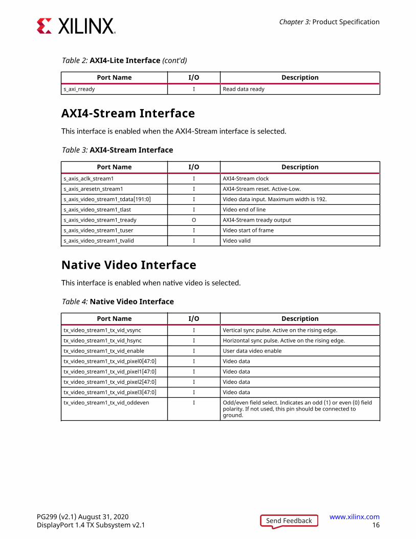
Table 2: AXI4-Lite Interface (cont'd)
Port Name I/O Descriptions_axi_rready I Read data ready
AXI4-Stream InterfaceThis interface is enabled when the AXI4-Stream interface is selected.
Table 3: AXI4-Stream Interface
Port Name I/O Descriptions_axis_aclk_stream1 I AXI4-Stream clock
s_axis_aresetn_stream1 I AXI4-Stream reset. Active-Low.
s_axis_video_stream1_tdata[191:0] I Video data input. Maximum width is 192.
s_axis_video_stream1_tlast I Video end of line
s_axis_video_stream1_tready O AXI4-Stream tready output
s_axis_video_stream1_tuser I Video start of frame
s_axis_video_stream1_tvalid I Video valid
Native Video InterfaceThis interface is enabled when native video is selected.
Table 4: Native Video Interface
Port Name I/O Descriptiontx_video_stream1_tx_vid_vsync I Vertical sync pulse. Active on the rising edge.
tx_video_stream1_tx_vid_hsync I Horizontal sync pulse. Active on the rising edge.
tx_video_stream1_tx_vid_enable I User data video enable
tx_video_stream1_tx_vid_pixel0[47:0] I Video data
tx_video_stream1_tx_vid_pixel1[47:0] I Video data
tx_video_stream1_tx_vid_pixel2[47:0] I Video data
tx_video_stream1_tx_vid_pixel3[47:0] I Video data
tx_video_stream1_tx_vid_oddeven I Odd/even field select. Indicates an odd (1) or even (0) fieldpolarity. If not used, this pin should be connected toground.
Chapter 3: Product Specification
PG299 (v2.1) August 31, 2020 www.xilinx.comDisplayPort 1.4 TX Subsystem v2.1 16Send Feedback

MST InterfaceTable 5: MST Stream (<n> = stream number 2 to 4)
Port Name I/O Descriptions_axis_aclk_stream<n> I MST stream clock.
s_axis_aresetn_stream<n> I MST stream reset. Active-Low.
s_axis_video_stream<n>_tdata[191:0] I MST stream video data input.
s_axis_video_stream<n>_tlast I MST stream video end of line.
s_axis_video_stream<n>_tready O MST stream input ready.
s_axis_video_stream<n>_tuser I MST stream video start of frame.
s_axis_video_stream<n>_tvalid I MST stream video valid.
m_aclk_stream1 I Video pipe clock for stream1. Used in MST configuration.
m_aresetn_stream1 I Active-Low video pipe reset for stream 1. Used in MSTconfiguration.
m_aclk_stream2 I Video pipe clock for stream 2. Used in MST configuration.
m_aresetn_stream2 I Active-Low video pipe reset for stream 2. Used in MSTconfiguration.
tx_vid_clk_stream<n> I User data clock for MST stream n.
tx_vid_rst_stream<n> I Active-High user video reset.
tx_video_stream<n>_tx_vid_vsync I Vertical sync pulse. Active on the rising edge.
tx_video_stream<n>_tx_vid_hsync I Horizontal sync pulse. Active on the rising edge
tx_video_stream<n>_tx_vid_enable I User data video enable.
tx_video_stream<n>_tx_vid_pixel0[47:0] I Video data
tx_video_stream<n>_tx_vid_pixel1[47:0] I Video data
tx_video_stream<n>_tx_vid_pixel2[47:0] I Video data
tx_video_stream<n>_tx_vid_pixel3[47:0] I Video data
tx_video_stream<n>_tx_vid_oddeven I Odd/even field select. Indicates an odd (1) or even (0) fieldpolarity. If not used, this pin should be connected toground.
User PortsTable 6: User Ports
Port Name I/O Descriptiontx_vid_clk_stream1 I User video clock
tx_vid_rst_stream1 I User video reset. Active-High.
tx_hpd I Hot-plug detect signal to TX from RX
Chapter 3: Product Specification
PG299 (v2.1) August 31, 2020 www.xilinx.comDisplayPort 1.4 TX Subsystem v2.1 17Send Feedback

Audio AXI4-Stream InterfaceTable 7: Audio AXI4-Stream Interface
Port Name I/O Descriptions_axis_audio_ingress_aclk I AXI4-Stream clock.
s_axis_audio_ingress_aresetn I Active-Low reset.
s_axis_audio_ingress_tdata[31:0] I AXI4-Stream data input.[3:0] - Preamble Code• 4'b0001: Subframe1/ Start of audio block• 4'b0010: Subframe 1• 4’b0011: Subframe 2[27:4] - Audio Sample Word[28] - Validity Bit (V)[29] - User Bit (U)[30] - Channel Status (C)[31] - Parity (P)
s_axis_audio_ingress_tid[7:0] I [3:0] - Audio Channel ID[7:4] - Audio Packet Stream ID
s_axis_audio_ingress_tvalid I Valid indicator for audio data from master.
s_axis_audio_ingress_tready O Ready indicator from DisplayPort source.
External Video PHY Sideband Status InterfaceTable 8: External Video PHY Sideband Status Interface
Port Name I/O Descriptions_axis_phy_tx_sb_status_tdata[7:0] O Sideband status to Video PHY
s_axis_phy_tx_sb_status_tready I Sideband status ready input from Video PHY
s_axis_phy_tx_sb_status_tvalid O Sideband status data valid to Video PHY
External Video PHY Clock InterfaceTable 9: External Video PHY Clock Interface
Port Name I/O Descriptiontx_lnk_clk I Link clock input from external Video PHY
Chapter 3: Product Specification
PG299 (v2.1) August 31, 2020 www.xilinx.comDisplayPort 1.4 TX Subsystem v2.1 18Send Feedback

External Video PHY Lane n InterfaceTable 10: External Video PHY Lane n Interface
Port Name1 I/O Descriptionm_axis_lnk_tx_lanen_tdata[31:0] O Lanen Data to External Video PHY
m_axis_lnk_tx_lanen_tvalid O Lanen Data Valid to External Video PHY
m_axis_lnk_tx_lanen_tready I Lanen Data Ready from External Video PHY
m_axis_lnk_tx_lanen_tuser[11:0] O Lanen User data out to External Video PHY
Notes:1. n = 0 to Lane_Count -1.
HDCP Key InterfaceTable 11: Interrupt Interface
Port Name I/O Descriptionhdcp_ext_clk I HDCP external clock
hdcp_key_aclk I HDCP key clock
hdcp_key_aresetn I Key Interface reset. Active-Low
hdcp_key_tdata[63:0] I AXI4-Stream Key Tdata
hdcp_key_last I AXI4-Stream Key Tlast
hdcp_key_tready O AXI4-Stream Key Tready
hdcp_key_tuser[7:0] I AXI4-Stream Key TUSER. KMB should send the Key numberfrom 0 to 41.0 corresponds to KSV and 1 to 40 are the HDCP Keys count.
hdcp_key_tvalid I AXI4-Stream Key TValid
reg_key_sel[2:0] O To select the one of the eight sets of 40 keys.
start_key_transmit O An Active-High pulse that is used to start key transmit.
AUX SignalsTable 12: AUX Signals
Port Name I/O Descriptionaux_tx_io_n O Negative polarity AUX Manchester-II data.
aux_tx_io_p O Positive polarity AUX Manchester-II data.
aux_tx_channel_in_p I Positive polarity AUX channel input. Valid when AUX IO Typeis unidirectional
aux_tx_channel_in_n I Negative polarity AUX channel input. Valid when AUX IOType is unidirectional
aux_tx_channel_out_p O Positive polarity AUX channel Output. Valid when AUX IOType is unidirectional
Chapter 3: Product Specification
PG299 (v2.1) August 31, 2020 www.xilinx.comDisplayPort 1.4 TX Subsystem v2.1 19Send Feedback

Table 12: AUX Signals (cont'd)
Port Name I/O Descriptionaux_tx_channel_out_n O Negative Polarity AUX channel output. Valid when AUX IO
Type is unidirectional
aux_tx_data_out O AUX data out. Valid when AUX IO buffer location is external
aux_tx_data_in I AUX data input. Valid when AUX IO buffer location isexternal
aux_tx_data_en_out_n O AUX data output enable. Active-Low. Valid only when AUX IObuffer location is external
Interrupt InterfaceTable 13: Interrupt Interface
Port Name I/O Descriptiondptxss_dp_irq O DisplayPort 1.4 TX IP interrupt out
dptxss_hdcp_irq O HDCP IP interrupt out
dptxss_timer_irq O AXI Timer IP interrupt output valid only when HDCP isenabled
Register SpaceThis section details registers available in the DisplayPort 1.4 TX Subsystem. The address map issplit into following regions:
• VTC 0 (Up to 3 for 4 streams in MST)
• DisplayPort TX IP
• HDCP Controller
Video Timing Controller RegistersFor details about the Video Timing Controller (VTC) registers, see the Video Timing ControllerLogiCORE IP Product Guide (PG016).
DisplayPort RegistersThe DisplayPort Configuration Data is implemented as a set of distributed registers which can beread or written from the AXI4-Lite interface. These registers are considered to be synchronous tothe AXI4-Lite domain and asynchronous to all others.
Chapter 3: Product Specification
PG299 (v2.1) August 31, 2020 www.xilinx.comDisplayPort 1.4 TX Subsystem v2.1 20Send Feedback

For parameters that might change while being read from the configuration space, two scenariosmight exist. In the case of single bits, either the new value or the old value is read as valid data. Inthe case of multiple bit fields, a lock bit might be used to prevent the status values from beingupdated while the read is occurring. For multi-bit configuration data, a toggle bit is usedindicating that the local values in the functional core should be updated.
Any bits not specified in the following tables are considered reserved and returns 0 upon read.The power on reset values of all the registers are 0 unless it is specified in the definition. Onlyaddress offsets are listed and the base addresses are configured by the AXI Interconnect.
Link Configuration Field
Table 14: Link Configuration Field
Offset AccessType Description
0x000 R/W LINK_BW_SET. Main link bandwidth setting. The register uses the same values as thosesupported by the DPCD register of the same name in the sink device.[7:0] - LINK_BW_SET: Sets the value of the main link bandwidth for the sink device.• 0x06 = 1.62 Gb/s• 0x0A = 2.7 Gb/s• 0x14 = 5.4 Gb/s• 0x1E = 8.1 Gb/s
0x004 R/W LANE_COUNT_SET. Sets the number of lanes used by the source in transmitting data.[4:0] - Set to 1, 2, or 4
0x008 R/W ENHANCED_FRAME_EN[0] - Set to 1 by the source to enable the enhanced framing symbol sequence.
0x00C R/W TRAINING_PATTERN_SET. Sets the link training mode.[2:0] - Set the link training pattern according to the 2-bit code.• 000 = Training off• 001 = Training pattern 1, used for clock recovery• 010 = Training pattern 2, used for channel equalization• 011 = Training pattern 3, used for channel equalization• 111 = Training pattern 4, used for channel equalization
0x010 R/W LINK_QUAL_PATTERN_SET. Transmit the link quality pattern.[2:0] - Enable transmission of the link quality test patterns.• 000 = Link quality test pattern not transmitted• 001 = D10.2 test pattern (unscrambled) transmitted• 010 = Symbol Error Rate measurement pattern• 011 = PRBS7 transmitted• 100 = Custom 80-bit pattern• 101 = HBR2 compliance pattern
0x014 R/W SCRAMBLING_DISABLE. Set to 1 when the transmitter has disabled the scrambler andtransmits all symbols.[0] - Disable scrambling.
Chapter 3: Product Specification
PG299 (v2.1) August 31, 2020 www.xilinx.comDisplayPort 1.4 TX Subsystem v2.1 21Send Feedback
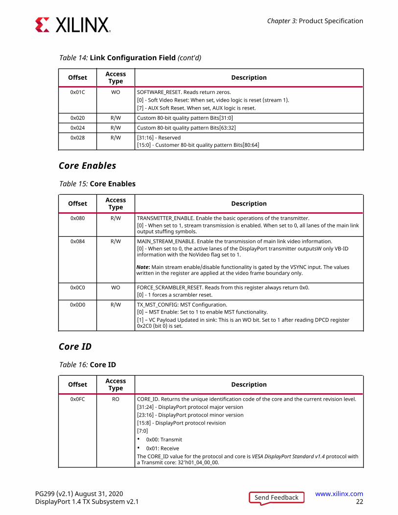
Table 14: Link Configuration Field (cont'd)
Offset AccessType Description
0x01C WO SOFTWARE_RESET. Reads return zeros.[0] - Soft Video Reset: When set, video logic is reset (stream 1).[7] - AUX Soft Reset. When set, AUX logic is reset.
0x020 R/W Custom 80-bit quality pattern Bits[31:0]
0x024 R/W Custom 80-bit quality pattern Bits[63:32]
0x028 R/W [31:16] - Reserved[15:0] - Customer 80-bit quality pattern Bits[80:64]
Core Enables
Table 15: Core Enables
Offset AccessType Description
0x080 R/W TRANSMITTER_ENABLE. Enable the basic operations of the transmitter.[0] - When set to 1, stream transmission is enabled. When set to 0, all lanes of the main linkoutput stuffing symbols.
0x084 R/W MAIN_STREAM_ENABLE. Enable the transmission of main link video information.[0] - When set to 0, the active lanes of the DisplayPort transmitter outputsW only VB-IDinformation with the NoVideo flag set to 1.
Note: Main stream enable/disable functionality is gated by the VSYNC input. The valueswritten in the register are applied at the video frame boundary only.
0x0C0 WO FORCE_SCRAMBLER_RESET. Reads from this register always return 0x0.[0] - 1 forces a scrambler reset.
0x0D0 R/W TX_MST_CONFIG: MST Configuration.[0] – MST Enable: Set to 1 to enable MST functionality.[1] – VC Payload Updated in sink: This is an WO bit. Set to 1 after reading DPCD register0x2C0 (bit 0) is set.
Core ID
Table 16: Core ID
Offset AccessType Description
0x0FC RO CORE_ID. Returns the unique identification code of the core and the current revision level.[31:24] - DisplayPort protocol major version[23:16] - DisplayPort protocol minor version[15:8] - DisplayPort protocol revision[7:0]• 0x00: Transmit• 0x01: ReceiveThe CORE_ID value for the protocol and core is VESA DisplayPort Standard v1.4 protocol witha Transmit core: 32’h01_04_00_00.
Chapter 3: Product Specification
PG299 (v2.1) August 31, 2020 www.xilinx.comDisplayPort 1.4 TX Subsystem v2.1 22Send Feedback

AUX Channel Interface
Table 17: AUX Channel Interface
Offset AccessType Description
0x100 R/W AUX_COMMAND_REGISTER. Initiates AUX channel commands of the specified length.[12] - Address only transfer enable. When this bit is set to 1, the source initiates Addressonly transfers (STOP is sent after the command).[11:8] - AUX Channel Command.• 0x8 = AUX Write• 0x9 = AUX Read• 0x0 = IC Write• 0x4 = IC Write MOT• 0x1 = IC Read• 0x5 = IC Read MOT• 0x2 = IC Write Status[3:0] - Specifies the number of bytes to transfer with the current command. The range ofthe register is 0 to 15 indicating between 1 and 16 bytes of data.
0x104 WO AUX_WRITE_FIFO. FIFO containing up to 16 bytes of write data for the current AUX channelcommand.[7:0] - AUX Channel byte data.
0x108 R/W AUX_ADDRESS. Specifies the address for the current AUX channel command.[19:0] - 20-bit address for the start of the AUX Channel burst.
0x10C R/W AUX_CLOCK_DIVIDER. Contains the clock divider value for generating the internal 1 MHzclock from the AXI4-Lite host interface clock. The clock divider register provides integerdivision only and does not support fractional AXI4-Lite clock rates (for example, set to 75 fora 75 MHz AXI4-Lite clock).[15:8] - The number of AXI4-Lite clocks (defined by the AXI4-Lite clock name: s_axi_aclk)equivalent to the recommended width of AUX pulse. Allowable values include: 8,16,24,32,40and 48.[7:0] - Clock divider value.From DisplayPort Protocol spec, AUX Pulse Width range = 0.4 to 0.6 µs.For example, for AXI4-Lite clock of 50 MHz (= 20 ns), the filter width, when set to 24, falls inthe allowable range as defined by the protocol spec.((20 × 24 = 480))Program a value of 24 in this register.
0x110 RC TX_USER_FIFO_OVERFLOW. Indicates an overflow in the user FIFO. The event can occur ifthe video rate does not match the TU size programming.[0] - FIFO_OVERFLOW_FLAG: 1 indicates that the internal FIFO has detected an overflowcondition. This bit clears upon read.
0x130 RO INTERRUPT_SIGNAL_STATE. Contains the raw signal values for those conditions which mightcause an interrupt.[3] - REPLY_TIMEOUT: 1 indicates that a reply timeout has occurred.[2] - REPLY_STATE: 1 indicates that a reply is currently being received.[1] - REQUEST_STATE: 1 indicates that a request is currently being sent.[0] - HPD_STATE: Contains the raw state of the HPD pin on the DisplayPort connector.
0x134 RO AUX_REPLY_DATA. Maps to the internal FIFO which contains up to 16 bytes of informationreceived during the AUX channel reply. Reply data is read from the FIFO starting with byte0. The number of bytes in the FIFO corresponds to the number of bytes requested.[7:0] - AUX reply data
Chapter 3: Product Specification
PG299 (v2.1) August 31, 2020 www.xilinx.comDisplayPort 1.4 TX Subsystem v2.1 23Send Feedback

Table 17: AUX Channel Interface (cont'd)
Offset AccessType Description
0x138 RO AUX_REPLY_CODE. Reply code received from the most recent AUX Channel request. TheAUX Reply Code corresponds to the code from the DisplayPort Standard.
Note: The core does not retry any commands that were Deferred or Not Acknowledged.
[3:2]• 00 = I2C ACK• 01 = I2C NACK• 10 = I2C DEFER[1:0]• 00 = AUX ACK• 01 = AUX NACK• 10 = AUX DEFER
0x13C R/W AUX_REPLY_COUNT. Provides an internal counter of the number of AUX reply transactionsreceived on the AUX Channel. Writing to this register clears the count.[7:0] - Current reply count.
0x140 RC INTERRUPT_STATUS. Source core interrupt status register. A read from this register clearsall values. Write operation is illegal and clears the values.[9] - Audio packet ID mismatch interrupt, sets when incoming audio packet ID over AXI4-Stream interface does not match with the info frame packet stream ID.[5] - EXT_PKT_TXD: Extended packet is transmitted and controller is ready to accept newpacket. Extended packet address space can also be used to send the audio copymanagement packet/ISRC packet/VSC packets.[4] - HPD_PULSE_DETECTED: A pulse on the HPD line was detected. The duration of thepulse can be determined by reading 0x150.[3] - REPLY_TIMEOUT: A reply timeout has occurred.[2] - REPLY_RECEIVED: An AUX reply transaction has been detected.[1] - HPD_EVENT: The core has detected the presence of the HPD signal. This interruptasserts immediately after the detection of HPD and after the loss of HPD for 2 ms.[0] - HPD_IRQ: An IRQ framed with the proper timing on the HPD signal has been detected.
0x144 R/W INTERRUPT_MASK. Masks the specified interrupt sources from asserting the axi_init signal.When set to a 1, the specified interrupt source is masked.This register resets to all 1s at power up. The respective MASK bit controls the assertion ofaxi_int only and does not affect events updated in the INTERRUPT_STATUS register.[9] - Mask Audio packet ID mismatch interrupt.[5] - EXT_PKT_TXD: Mask Extended Packet Transmitted interrupt.[4] - HPD_PULSE_DETECTED: Mask HPD Pulse interrupt.[3] - REPLY_TIMEOUT: Mask reply timeout interrupt.[2] - REPLY_RECEIVED: Mask reply received interrupt.[1] - HPD_EVENT: Mask HPD event interrupt.[0] - HPD_IRQ: Mask HPD IRQ interrupt.
0x148 RO REPLY_DATA_COUNT. Returns the total number of data bytes actually received during atransaction. This register does not use the length byte of the transaction header.[4:0] - Total number of data bytes received during the reply phase of the AUX transaction.
Chapter 3: Product Specification
PG299 (v2.1) August 31, 2020 www.xilinx.comDisplayPort 1.4 TX Subsystem v2.1 24Send Feedback

Table 17: AUX Channel Interface (cont'd)
Offset AccessType Description
0x14C RO REPLY_STATUS[15:12] - RESERVED[11:4] - REPLY_STATUS_STATE: Internal AUX reply state machine status bits.[3] - REPLY_ERROR: When set to a 1, the AUX reply logic has detected an error in the reply tothe most recent AUX transaction.[2] - REQUEST_IN_PROGRESS: The AUX transaction request controller sets this bit to a 1while actively transmitting a request on the AUX serial bus. The bit is set to 0 when the AUXtransaction request controller is idle.[1] - REPLY_IN_PROGRESS: The AUX reply detection logic sets this bit to a 1 while receiving areply on the AUX serial bus. The bit is 0 otherwise.[0] - REPLY_RECEIVED: This bit is set to 0 when the AUX request controller begins sendingbits on the AUX serial bus. The AUX reply controller sets this bit to 1 when a complete andvalid reply transaction has been received.
0x150 RO HPD_DURATION[15:0] - Duration of the HPD pulse in µs.
0x154 RO Free running counter incrementing for every 1 MHz.
Main Stream Attributes
For more details on the DisplayPort Standard, see the VESA DisplayPort Standard v1.4.
Table 18: Main Stream Attributes
Offset AccessType Description
0x180 R/W MAIN_STREAM_HTOTAL. Specifies the total number of clocks in the horizontal framingperiod for the main stream video signal.[15:0] - Horizontal line length total in clocks.
0x184 R/W MAIN_STREAM_VTOTAL. Provides the total number of lines in the main stream video frame.[15:0] - Total number of lines per video frame.
0x188 R/W MAIN_STREAM_POLARITY. Provides the polarity values for the video sync signals. Polarityinformation is packed and sent in the MSA packet. See the Main Stream Attribute DataTransport section of the VESA DisplayPort Standard (VESA website).0 = Active-High1 = Active-Low[1] - VSYNC_POLARITY: Polarity of the vertical sync pulse.[0] - HSYNC_POLARITY: Polarity of the horizontal sync pulse.
0x18C R/W MAIN_STREAM_HSWIDTH. Sets the width of the horizontal sync pulse.[14:0] - Horizontal sync width in clock cycles.
0x190 R/W MAIN_STREAM_VSWIDTH. Sets the width of the vertical sync pulse.[14:0] - Width of the vertical sync in lines.
0x194 R/W MAIN_STREAM_HRES. Horizontal resolution of the main stream video source.[15:0] - Number of active pixels per line of the main stream video.
0x198 R/W MAIN_STREAM_VRES. Vertical resolution of the main stream video source.[15:0] - Number of active lines of video in the main stream video source.
Chapter 3: Product Specification
PG299 (v2.1) August 31, 2020 www.xilinx.comDisplayPort 1.4 TX Subsystem v2.1 25Send Feedback

Table 18: Main Stream Attributes (cont'd)
Offset AccessType Description
0x19C R/W MAIN_STREAM_HSTART. Number of clocks between the leading edge of the horizontal syncand the start of active data.[15:0] - Horizontal start clock count.
0x1A0 R/W MAIN_STREAM_VSTART. Number of lines between the leading edge of the vertical sync andthe first line of active data.[15:0] - Vertical start line count.
0x1A4 R/W MAIN_STREAM_MISC0. Miscellaneous stream attributes.[7:0] - Implements the attribute information contained in the DisplayPort MISC0 registerdescribed in section 2.2.4 of the standard.[12] - 0: Default Behavior. 1: Enables mode to sync Ext packet transmission with Vsyncevent.[11] - Maud control (Advanced Users)[10] - Audio Only Mode. When enabled, controller inserts information/timestamp packetsevery 512 BS symbols. By default the value is 0.[9] - Sync/Async Mode for Audio[8] - Override Audio Clocking Mode[7:5] - Bit depth per color/component[4] - YCbCr Colorimetry[3] - Dynamic Range[2:1] - Component Format[0] - Synchronous Clock
0x1A8 R/W MAIN_STREAM_MISC1. Miscellaneous stream attributes.[7:0] - Implements the attribute information contained in the DisplayPort MISC1 registerdescribed in section 2.2.4 of the standard.[5:3] - Reserved[2:1] - Stereo video attribute[0] - Interlaced vertical total even
0x1AC R/W M-VID. If synchronous clocking mode is used, this register must be written with the M valueas described in section 2.2.3 of the standard. When in asynchronous clocking mode, the Mvalue for the video stream is automatically computed by the source core and written to themain stream. These values are not written into the M-VID register for readback.[23:0] - Unsigned M value.
0x1B0 R/W TRANSFER_UNIT_SIZE. Sets the size of a transfer unit in the framing logic On reset, transfersize is set to 64. This register must be written as described in section 2.2.1.4.1 of thestandard.[6:0] - This number should be 32 or 64 and is set to a fixed value that depends on theinbound video mode. Note that bit 0 cannot be written (the transfer unit size is alwayseven).
0x1B4 R/W N-VID. If synchronous clocking mode is used, this register must be written with the N valueas described in section 2.2.3 of the standard. When in asynchronous clocking mode, the Mvalue for the video stream is automatically computed by the source core and written to themain stream. These values are not written into the N-VID register for readback.[23:0] - Unsigned N value.
0x1B8 R/W USER_PIXEL_WIDTH. Selects the width of the user data input port. Use quad pixel mode inMST. In SST, the user pixel width should always be equal to the active lane count generatedin hardware.[2:0]:• 1 - Single pixel wide interface• 2 - Dual pixel wide interface. Valid for designs with 2 or 4 lanes.• 4 - Quad pixel wide interface Valid for designs with 4 lanes only.
Chapter 3: Product Specification
PG299 (v2.1) August 31, 2020 www.xilinx.comDisplayPort 1.4 TX Subsystem v2.1 26Send Feedback

Table 18: Main Stream Attributes (cont'd)
Offset AccessType Description
0x1BC R/W USER_DATA_COUNT_PER_LANE. This register is used to translate the number of pixels perline to the native internal 16-bit datapath.If (HRES × bits per pixel) is divisible by 16, then word_per_line = ((HRES × bits per pixel)/16)Elseword_per_line = (INT((HRES × bits per pixel)/16)) + 1For single-lane design:Set USER_DATA_COUNT_PER_LANE = words_per_line - 1For 2-lane design:If words_per_line is divisible by 2, then set USER_DATA_COUNT_PER_LANE = words_per_line -2ElseSet USER_DATA_COUNT_PER_LANE = words_per_line + MOD(words_per_line,2) - 2For 4-lane design:If words_per_line is divisible by 4, then set USER_DATA_COUNT_PER_LANE = words_per_line -4ElseSet USER_DATA_COUNT_PER_LANE = words_per_line + MOD(words_per_line,4) - 4
Note: When MST mode is selected, irrespective of the user selected value of "number oflanes", "USER_DATA_COUNT_PER_LANE" should always be calculated, considering numberof lanes as 4. This is because, DP core always works in 4 lane mode in MST.
0x1C0 R/W MAIN_STREAM_INTERLACED. Informs the DisplayPort transmitter main link that the sourcevideo is interlaced. By setting this bit to a 1, the core sets the appropriate fields in the VBIDvalue and Main Stream Attributes. This bit must be set to a 1 for the proper transmission ofinterlaced sources.[0] - Set to a 1 when transmitting interlaced images.
0x1C4 R/W MIN_BYTES_PER_TU. Programs source to use MIN number of bytes per transfer unit. Thecalculation should be done based on the DisplayPort Standard.[6:0] - Set the value to INT((VIDEO_BW/LINK_BW)*TRANSFER_UNIT_SIZE)
0x1C8 R/W FRAC_BYTES_PER_TU. Calculating MIN bytes per TU is often not a whole number. Thisregister is used to hold the fractional component.[9:0] - The fraction part of ((VIDEO_BW/LINK_BW) × TRANSFER_UNIT_SIZE) scaled by 1024 isprogrammed in this register.
0x1CC R/W INIT_WAIT. This register defines the number of initial wait cycles at the start of a new lineby the Framing logic. This allows enough data to be buffered in the input FIFO. The defaultvalue of INIT_WAIT is 0x20.If (MIN_BYTES_PER_TU ≤ 4)• [6:0] - Set INIT_WAIT to 64Else if color format is RGB/YCbCr_444• [6:0] - Set INIT_WAIT to (TRANSFER_UNIT_SIZE - MIN_BYTES_PER_TU)Else if color format is YCbCr_422• [6:0] - Set INIT_WAIT to (TRANSFER_UNIT_SIZE - MIN_BYTES_PER_TU)/2Else if color format is Y_Only• [6:0] - Set INIT_WAIT to (TRANSFER_UNIT_SIZE - MIN_BYTES_PER_TU)/3
Chapter 3: Product Specification
PG299 (v2.1) August 31, 2020 www.xilinx.comDisplayPort 1.4 TX Subsystem v2.1 27Send Feedback

PHY Configuration Status
Table 19: PHY Configuration Status
Offset AccessType Description
0x280 RO PHY_STATUS. Provides the current status from the PHY.[31:30] - Unused, read as 0.[29:28] - Transmitter buffer status, lane 3.[27:26] - Unused, read as 0.[25:24] - Transmitter buffer status, lane 2.[23:22] - Unused, read as 0.[21:20] - Transmitter buffer status, lane 1.[19:18] - Unused, read as 0.[17:16] - Transmitter buffer status, lane 0.[15:7] - Unused, read as 0.[6] - FPGA fabric clock PLL locked.[5] - PLL for lanes 2 and 3 locked.[4] - PLL for lanes 0 and 1 locked.[3:2] - Reset done for lanes 2 and 3.[1:0] - Reset done for lanes 0 and 1.
MST Mode Registers
Table 20: DisplayPort Source Core Configuration Space - MST Interface
Offset R/W Definition0x500 RW MAIN_STREAM_HTOTAL_STREAM2. Specifies the total number of clocks in the horizontal
framing period for the main stream video signal.[15:0] - Horizontal line length total in clocks.
0x504 RW MAIN_STREAM_VTOTAL_STREAM2. Provides the total number of lines in the main streamvideo frame.[15:0] - Total number of lines per video frame.
0x508 RW MAIN_STREAM_POLARITY_STREAM2. Provides the polarity values for the video sync signals.[1] - VSYNC_POLARITY: Polarity of the vertical sync pulse.[0] - HSYNC_POLARITY: Polarity of the horizontal sync pulse.
0x50C RW MAIN_STREAM_HSWIDTH_STREAM2. Sets the width of the horizontal sync pulse.[14:0] - Horizontal sync width in clock cycles.
0x510 RW MAIN_STREAM_VSWIDTH_STREAM2. Sets the width of the vertical sync pulse.[14:0] - Width of the vertical sync in lines.
0x514 RW MAIN_STREAM_HRES_STREAM2. Horizontal resolution of the main stream video source.[15:0] - Number of active pixels per line of the main stream video.
0x518 RW MAIN_STREAM_VRES_STREAM2. Vertical resolution of the main stream video source.[15:0] - Number of active lines of video in the main stream video source.
0x51C RW MAIN_STREAM_HSTART_STREAM2. Number of clocks between the leading edge of thehorizontal sync and the start of active data.[15:0] - Horizontal start clock count.
Chapter 3: Product Specification
PG299 (v2.1) August 31, 2020 www.xilinx.comDisplayPort 1.4 TX Subsystem v2.1 28Send Feedback

Table 20: DisplayPort Source Core Configuration Space - MST Interface (cont'd)
Offset R/W Definition0x520 RW MAIN_STREAM_VSTART_STREAM2. Number of lines between the leading edge of the vertical
sync and the first line of active data.[15:0] - Vertical start line count.
0x524 RW MAIN_STREAM_MISC0_STREAM2. Miscellaneous stream attributes.[7:0] - Implements the attribute information contained in the DisplayPort MISC0 registerdescribed in section 2.2.4 of the standard.[0] -Synchronous Clock.[2:1] - Component Format.[3] - Dynamic Range.[4] - YCbCr Colorimetry.[7:5] - Bit depth per color/component.
0x528 RW MAIN_STREAM_MISC1_STREAM2. Miscellaneous stream attributes.[7:0] - Implements the attribute information contained in the DisplayPort MISC1 registerdescribed in section 2.2.4 of the standard.[0] - Interlaced vertical total even.[2:1] - Stereo video attribute.[6:3] - Reserved.
0x52C RW M-VID_STREAM2. If synchronous clocking mode is used, this register must be written withthe M value as described in section 2.2.3 of the standard. When in asynchronous clockingmode, the M value for the video stream as automatically computed by the source core andwritten to the main stream. These values are not written into the M-VID register forreadback.[23:0] - Unsigned M value.
0x530 RW TRANSFER_UNIT_SIZE_STREAM2. Sets the size of a transfer unit in the framing logic Onreset, transfer size is set to 64.[6:0] - This number should be in the range of 32 to 64 and is set to a fixed value thatdepends on the inbound video mode. Note that bit 0 cannot be written (the transfer unitsize is always even).
0x534 RW N-VID_STREAM2. If synchronous clocking mode is used, this register must be written withthe N value as described in section 2.2.3 of the standard. When in asynchronous clockingmode, the M value for the video stream as automatically computed by the source core andwritten to the main stream. These values are not written into the N-VID register forreadback.[23:0] - Unsigned N value.
0x538 RW USER_PIXEL_WIDTH_STREAM2. Selects the width of the user data input port. Use quad pixelmode in MST.[2:0]:• 1 = Single pixel wide interface• 2 = Dual pixel wide interface• 4 = Quad pixel wide interface
Chapter 3: Product Specification
PG299 (v2.1) August 31, 2020 www.xilinx.comDisplayPort 1.4 TX Subsystem v2.1 29Send Feedback

Table 20: DisplayPort Source Core Configuration Space - MST Interface (cont'd)
Offset R/W Definition0x53C RW USER_DATA_COUNT_PER_LANE_STREAM2. This register is used to translate the number of
pixels per line to the native internal datapath.If (HRES × bits per pixel) is divisible by 16, thenword_per_line = ((HRES * bits per pixel)/16)Elseword_per_line = (INT((HRES × bits per pixel)/16)) + 1For single-lane design:Set USER_DATA_COUNT_PER_LANE = words_per_line - 1For 2-lane design:If words_per_line is divisible by 2, thenSet USER_DATA_COUNT_PER_LANE = words_per_line - 2ElseSet USER_DATA_COUNT_PER_LANE = words_per_line + MOD(words_per_line,2) - 2For 4-lane design:If words_per_line is divisible by 4, thenSet USER_DATA_COUNT_PER_LANE = words_per_line - 4ElseSet USER_DATA_COUNT_PER_LANE = words_per_line + MOD(words_per_line,4) - 4
0x540 RW MAIN_STREAM_INTERLACED_STREAM2. Informs the DisplayPort transmitter main link thatthe source video is interlaced. By setting this bit to a 1, the core will set the appropriatefields in the VBID value and Main Stream Attributes. This bit must be set to 1 for the propertransmission of interlaced sources.[0] - Set to 1 when transmitting interlaced images.
0x544 RW MIN_BYTES_PER_TU_STREAM2: Programs source to use MIN number of bytes per transferunit. The calculation should be done based on the DisplayPort Standard.[7:0] - Set the value to INT((LINK_BW/VIDEO_BW)*TRANSFER_UNIT_SIZE)
0x548 RW FRAC_BYTES_PER_TU_STREAM2: Calculating MIN bytes per TU will often not be a wholenumber. This register is used to hold the fractional component.[9:0] - The fraction part of ((LINK_BW/VIDEO_BW)*TRANSFER_UNIT_SIZE) scaled by 1000 isprogrammed in this register.
0x54C RW INIT_WAIT_STREAM2: This register defines the number of initial wait cycles at the start of anew line by the Framing logic. This allows enough data to be buffered in the input FIFO.If (MIN_BYTES_PER_TU ≤ 4)[6:0] - Set INIT_WAIT to 64else if color format is RGB/YCbCr_444[6:0] - Set INIT_WAIT to (TRANSFER_UNIT_SIZE - MIN_BYTES_PER_TU)else if color format is YCbCr_422[6:0] - Set INIT_WAIT to (TRANSFER_UNIT_SIZE - MIN_BYTES_PER_TU)/2else if color format is Y_Only[6:0] - Set INIT_WAIT to (TRANSFER_UNIT_SIZE - MIN_BYTES_PER_TU)/3
0x550 RW MAIN_STREAM_HTOTAL_STREAM3. Specifies the total number of clocks in the horizontalframing period for the main stream video signal.[15:0] - Horizontal line length total in clocks.
0x554 RW MAIN_STREAM_VTOTAL_STREAM3. Provides the total number of lines in the main streamvideo frame.[15:0] - Total number of lines per video frame.
0x558 RW MAIN_STREAM_POLARITY_STREAM3. Provides the polarity values for the video sync signals.[1] - VSYNC_POLARITY: Polarity of the vertical sync pulse.[0] - HSYNC_POLARITY: Polarity of the horizontal sync pulse.
Chapter 3: Product Specification
PG299 (v2.1) August 31, 2020 www.xilinx.comDisplayPort 1.4 TX Subsystem v2.1 30Send Feedback
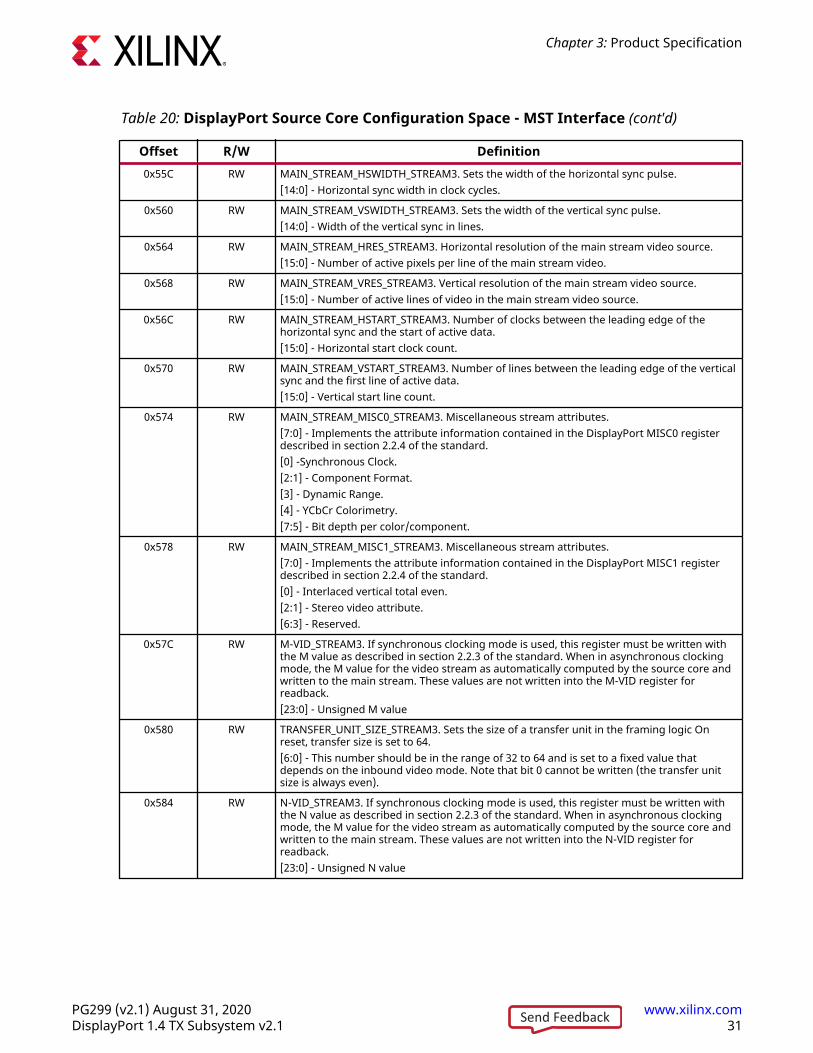
Table 20: DisplayPort Source Core Configuration Space - MST Interface (cont'd)
Offset R/W Definition0x55C RW MAIN_STREAM_HSWIDTH_STREAM3. Sets the width of the horizontal sync pulse.
[14:0] - Horizontal sync width in clock cycles.
0x560 RW MAIN_STREAM_VSWIDTH_STREAM3. Sets the width of the vertical sync pulse.[14:0] - Width of the vertical sync in lines.
0x564 RW MAIN_STREAM_HRES_STREAM3. Horizontal resolution of the main stream video source.[15:0] - Number of active pixels per line of the main stream video.
0x568 RW MAIN_STREAM_VRES_STREAM3. Vertical resolution of the main stream video source.[15:0] - Number of active lines of video in the main stream video source.
0x56C RW MAIN_STREAM_HSTART_STREAM3. Number of clocks between the leading edge of thehorizontal sync and the start of active data.[15:0] - Horizontal start clock count.
0x570 RW MAIN_STREAM_VSTART_STREAM3. Number of lines between the leading edge of the verticalsync and the first line of active data.[15:0] - Vertical start line count.
0x574 RW MAIN_STREAM_MISC0_STREAM3. Miscellaneous stream attributes.[7:0] - Implements the attribute information contained in the DisplayPort MISC0 registerdescribed in section 2.2.4 of the standard.[0] -Synchronous Clock.[2:1] - Component Format.[3] - Dynamic Range.[4] - YCbCr Colorimetry.[7:5] - Bit depth per color/component.
0x578 RW MAIN_STREAM_MISC1_STREAM3. Miscellaneous stream attributes.[7:0] - Implements the attribute information contained in the DisplayPort MISC1 registerdescribed in section 2.2.4 of the standard.[0] - Interlaced vertical total even.[2:1] - Stereo video attribute.[6:3] - Reserved.
0x57C RW M-VID_STREAM3. If synchronous clocking mode is used, this register must be written withthe M value as described in section 2.2.3 of the standard. When in asynchronous clockingmode, the M value for the video stream as automatically computed by the source core andwritten to the main stream. These values are not written into the M-VID register forreadback.[23:0] - Unsigned M value
0x580 RW TRANSFER_UNIT_SIZE_STREAM3. Sets the size of a transfer unit in the framing logic Onreset, transfer size is set to 64.[6:0] - This number should be in the range of 32 to 64 and is set to a fixed value thatdepends on the inbound video mode. Note that bit 0 cannot be written (the transfer unitsize is always even).
0x584 RW N-VID_STREAM3. If synchronous clocking mode is used, this register must be written withthe N value as described in section 2.2.3 of the standard. When in asynchronous clockingmode, the M value for the video stream as automatically computed by the source core andwritten to the main stream. These values are not written into the N-VID register forreadback.[23:0] - Unsigned N value
Chapter 3: Product Specification
PG299 (v2.1) August 31, 2020 www.xilinx.comDisplayPort 1.4 TX Subsystem v2.1 31Send Feedback

Table 20: DisplayPort Source Core Configuration Space - MST Interface (cont'd)
Offset R/W Definition0x588 RW USER_PIXEL_WIDTH_STREAM3. Selects the width of the user data input port. Use quad pixel
mode in MST.[2:0]:• 1 = Single pixel wide interface• 2 = Dual pixel wide interface• 4 = Quad pixel wide interface
0x58C RW USER_DATA_COUNT_PER_LANE_STREAM3. This register is used to translate the number ofpixels per line to the native internal 16-bit datapath.If (HRES * bits per pixel) is divisible by 16, thenword_per_line = ((HRES × bits per pixel)/16)Elseword_per_line = (INT((HRES × bits per pixel)/16)) + 1For single-lane design:Set USER_DATA_COUNT_PER_LANE = words_per_line - 1For 2-lane design:If words_per_line is divisible by 2, thenSet USER_DATA_COUNT_PER_LANE = words_per_line - 2ElseSet USER_DATA_COUNT_PER_LANE = words_per_line + MOD(words_per_line,2) - 2For 4-lane design:If words_per_line is divisible by 4, thenSet USER_DATA_COUNT_PER_LANE = words_per_line - 4ElseSet USER_DATA_COUNT_PER_LANE = words_per_line + MOD(words_per_line,4) - 4
0x590 RW MAIN_STREAM_INTERLACED_STREAM3. Informs the DisplayPort transmitter main link thatthe source video is interlaced. By setting this bit to a 1, the core will set the appropriatefields in the VBID value and Main Stream Attributes. This bit must be set to 1 for the propertransmission of interlaced sources.[0] - Set to 1 when transmitting interlaced images.
0x594 RW MIN_BYTES_PER_TU_STREAM3: Programs source to use MIN number of bytes per transferunit. The calculation should be done based on the DisplayPort Standard.[7:0] - Set the value to INT((LINK_BW/VIDEO_BW)*TRANSFER_UNIT_SIZE)
0x598 RW FRAC_BYTES_PER_TU_STREAM3: Calculating MIN bytes per TU is often not a whole number.This register is used to hold the fractional component.[9:0] - The fraction part of ((LINK_BW/VIDEO_BW) × TRANSFER_UNIT_SIZE) scaled by 1000 isprogrammed in this register.
0x59C RW INIT_WAIT_STREAM3: This register defines the number of initial wait cycles at the start of anew line by the Framing logic. This allows enough data to be buffered in the input FIFO.If (MIN_BYTES_PER_TU ≤ 4)[6:0] - Set INIT_WAIT to 64else if color format is RGB/YCbCr_444[6:0] - Set INIT_WAIT to (TRANSFER_UNIT_SIZE - MIN_BYTES_PER_TU)else if color format is YCbCr_422[6:0] - Set INIT_WAIT to (TRANSFER_UNIT_SIZE - MIN_BYTES_PER_TU)/2else if color format is Y_Only[6:0] - Set INIT_WAIT to (TRANSFER_UNIT_SIZE - MIN_BYTES_PER_TU)/3
0x5A0 RW MAIN_STREAM_HTOTAL_STREAM4. Specifies the total number of clocks in the horizontalframing period for the main stream video signal.[15:0] - Horizontal line length total in clocks.
Chapter 3: Product Specification
PG299 (v2.1) August 31, 2020 www.xilinx.comDisplayPort 1.4 TX Subsystem v2.1 32Send Feedback

Table 20: DisplayPort Source Core Configuration Space - MST Interface (cont'd)
Offset R/W Definition0x5A4 RW MAIN_STREAM_VTOTAL_STREAM4. Provides the total number of lines in the main stream
video frame.[15:0] - Total number of lines per video frame.
0x5A8 RW MAIN_STREAM_POLARITY_STREAM4. Provides the polarity values for the video sync signals.[1] - VSYNC_POLARITY: Polarity of the vertical sync pulse.[0] - HSYNC_POLARITY: Polarity of the horizontal sync pulse.
0x5AC RW MAIN_STREAM_HSWIDTH_STREAM4. Sets the width of the horizontal sync pulse.[14:0] - Horizontal sync width in clock cycles.
0x5B0 RW MAIN_STREAM_VSWIDTH_STREAM4. Sets the width of the vertical sync pulse.[14:0] - Width of the vertical sync in lines.
0x5B4 RW MAIN_STREAM_HRES_STREAM4. Horizontal resolution of the main stream video source.[15:0] - Number of active pixels per line of the main stream video.
0x5B8 RW MAIN_STREAM_VRES_STREAM4. Vertical resolution of the main stream video source.[15:0] - Number of active lines of video in the main stream video source.
0x5BC RW MAIN_STREAM_HSTART_STREAM4. Number of clocks between the leading edge of thehorizontal sync and the start of active data.[15:0] - Horizontal start clock count.
0x5C0 RW MAIN_STREAM_VSTART_STREAM4. Number of lines between the leading edge of the verticalsync and the first line of active data.[15:0] - Vertical start line count.
0x5C4 RW MAIN_STREAM_MISC0_STREAM4. Miscellaneous stream attributes.[7:0] - Implements the attribute information contained in the DisplayPort MISC0 registerdescribed in section 2.2.4 of the standard.[0] -Synchronous Clock.[2:1] - Component Format.[3] - Dynamic Range.[4] - YCbCr Colorimetry.[7:5] - Bit depth per color/component.
0x5C8 RW MAIN_STREAM_MISC1_STREAM4. Miscellaneous stream attributes.[7:0] - Implements the attribute information contained in the DisplayPort MISC1 registerdescribed in section 2.2.4 of the standard.[0] - Interlaced vertical total even.[2:1] - Stereo video attribute.[6:3] - Reserved.
0x5CC RW M-VID_STREAM4. If synchronous clocking mode is used, this register must be written withthe M value as described in section 2.2.3 of the standard. When in asynchronous clockingmode, the M value for the video stream as automatically computed by the source core andwritten to the main stream. These values are not written into the M-VID register forreadback.[23:0] - Unsigned M value.
0x5D0 RW TRANSFER_UNIT_SIZE_STREAM4. Sets the size of a transfer unit in the framing logic Onreset, transfer size is set to 64.[6:0] - This number should be in the range of 32 to 64 and is set to a fixed value thatdepends on the inbound video mode. Note that bit 0 cannot be written (the transfer unitsize is always even).
Chapter 3: Product Specification
PG299 (v2.1) August 31, 2020 www.xilinx.comDisplayPort 1.4 TX Subsystem v2.1 33Send Feedback

Table 20: DisplayPort Source Core Configuration Space - MST Interface (cont'd)
Offset R/W Definition0x5D4 RW N-VID_STREAM4. If synchronous clocking mode is used, this register must be written with
the N value as described in section 2.2.3 of the standard. When in asynchronous clockingmode, the M value for the video stream as automatically computed by the source core andwritten to the main stream. These values are not written into the N-VID register forreadback.[23:0] - Unsigned N value.
0x5D8 RW USER_PIXEL_WIDTH_STREAM4. Selects the width of the user data input port. Use quad pixelmode in MST.[2:0]:• 1 = Single pixel wide interface• 2 = Dual pixel wide interface• 4 = Quad pixel wide interface
0x5DC RW USER_DATA_COUNT_PER_LANE_STREAM4. This register is used to translate the number ofpixels per line to the native internal 16-bit datapath.If (HRES × bits per pixel) is divisible by 16, thenword_per_line = ((HRES × bits per pixel)/16)Elseword_per_line = (INT((HRES × bits per pixel)/16)) + 1For single-lane design:Set USER_DATA_COUNT_PER_LANE = words_per_line - 1For 2-lane design:If words_per_line is divisible by 2, thenSet USER_DATA_COUNT_PER_LANE = words_per_line - 2ElseSet USER_DATA_COUNT_PER_LANE = words_per_line + MOD(words_per_line,2) - 2For 4-lane design:If words_per_line is divisible by 4, thenSet USER_DATA_COUNT_PER_LANE = words_per_line - 4ElseSet USER_DATA_COUNT_PER_LANE = words_per_line + MOD(words_per_line,4) - 4
0x5E0 RW MAIN_STREAM_INTERLACED_STREAM4. Informs the DisplayPort transmitter main link thatthe source video is interlaced. By setting this bit to a 1, the core sets the appropriate fieldsin the VBID value and Main Stream Attributes. This bit must be set to 1 for the propertransmission of interlaced sources.[0] - Set to 1 when transmitting interlaced images.
0x5E4 RW MIN_BYTES_PER_TU_STREAM4. Programs source to use MIN number of bytes per transferunit. The calculation should be done based on the DisplayPort Standard.[7:0] - Set the value to INT((LINK_BW/VIDEO_BW)*TRANSFER_UNIT_SIZE)
0x5E8 RW FRAC_BYTES_PER_TU_STREAM4. Calculating MIN bytes per TU is often not a whole number.This register is used to hold the fractional component.[9:0] - The fraction part of ((LINK_BW/VIDEO_BW) × TRANSFER_UNIT_SIZE) scaled by 1000 isprogrammed in this register.
Chapter 3: Product Specification
PG299 (v2.1) August 31, 2020 www.xilinx.comDisplayPort 1.4 TX Subsystem v2.1 34Send Feedback

Table 20: DisplayPort Source Core Configuration Space - MST Interface (cont'd)
Offset R/W Definition0x5EC RW INIT_WAIT_STREAM4. This register defines the number of initial wait cycles at the start of a
new line by the Framing logic. This allows enough data to be buffered in the input FIFO.If (MIN_BYTES_PER_TU ≤ 4):[6:0] - Set INIT_WAIT to 64else if color format is RGB/YCbCr_444[6:0] - Set INIT_WAIT to (TRANSFER_UNIT_SIZE - MIN_BYTES_PER_TU)else if color format is YCbCr_422[6:0] - Set INIT_WAIT to (TRANSFER_UNIT_SIZE - MIN_BYTES_PER_TU)/2else if color format is Y_Only[6:0] - Set INIT_WAIT to (TRANSFER_UNIT_SIZE - MIN_BYTES_PER_TU)/3
0x800 to0x8FF
WO PAYLOAD_TABLE. This address space maps to the VC payload table that is maintained in thecore.[7:0] - Payload data
DisplayPort Audio Registers
The DisplayPort Audio registers are listed here.
Table 21: DisplayPort Audio
Offset AccessType Description
0x300 R/W TX_AUDIO_CONTROL. Enables audio stream packets in main link and provides buffercontrol.[19]: Set to 1 to mute the audio over link for MST STREAM 4. NA for SST[18]: Set to 1 to mute the audio over link for MST STREAM 3. NA for SST[17]: Set to 1 to mute the audio over link for MST STREAM 2. NA for SST[16]: Set to 1 to mute the audio over link for SST. in MST, set to 1 to mute the Audio onSTREAM 1[5:4]: Audio Enable for STREAM 4:5 in MST. Default is STREAM1[3]: Audio Enable for STREAM 4 in MST. NA for SST[2]: Audio Enable for STREAM 3 in MST. NA for SST[1]: Audio Enable for STREAM 2 in MST. NA for SST[0]: Audio Enable for SST. In MST, Audio Enable for STREAM 1
0x304 R/W TX_AUDIO_CHANNELS. Used to input active channel count. Transmitter collects audiosamples based on this information.[2:0] Channel Count
Chapter 3: Product Specification
PG299 (v2.1) August 31, 2020 www.xilinx.comDisplayPort 1.4 TX Subsystem v2.1 35Send Feedback

Table 21: DisplayPort Audio (cont'd)
Offset AccessType Description
0x308 WO TX_AUDIO_INFO_DATA.[31:0] Word formatted as per CEA 861-C Info Frame. Total of eight words should be writtenin following order:1st word -• [31:24] = HB3• [23:16] = HB2• [15:8] = HB1• [7:0] = HB02nd word - DB3,DB2,DB1,DB0....8th word - DB27,DB26,DB25,DB24The data bytes DB1...DBN of CEA Info frame are mapped as DB0-DBN-1.No protection is provided for wrong operations by software.
0x328 R/W TX_AUDIO_MAUD. M value of audio stream as computed by transmitter.[23:0] = Unsigned value computed when audio clock and link clock are synchronous.
0x32C R/W TX_AUDIO_NAUD. N value of audio stream as computed by transmitter.[23:0] = Unsigned value computed when audio clock and link clock are synchronous.
0x330 to0x350
WO TX_AUDIO_EXT_DATA.[31:0] = Word formatted as per Extension packet described in protocol standard.Extended packet is fixed to 32 Bytes length. The controller has buffer space for only oneextended packet. Extension packet address space can be used to send the audio Copymanagement packet/ISRC packet/VSC packets. TX is capable of sending any of thesepackets. VSC/EXT packets should use the same address space.A total of nine words should be written in following order:First word -• [31:24] = HB3• [23:16] = HB2• [15:8] = HB1• [7:0] = HB0Second word - DB3,DB2,DB1,DB0....9th word - DB31, DB30, DB29, DB28See the DisplayPort Standard for HB* definition.No protection is provided for wrong operations by software. This is a key-hole memory. So,nine writes to this address space is required.
HDCP RegistersFor details about the HDCP registers, see the HDCP 1.x Product Guide (PG224).
Chapter 3: Product Specification
PG299 (v2.1) August 31, 2020 www.xilinx.comDisplayPort 1.4 TX Subsystem v2.1 36Send Feedback

Chapter 4
Designing with the SubsystemThis chapter includes guidelines and additional information to facilitate designing with thesubsystem.
DisplayPort OverviewThe Source core moves a video stream from a standardized main link through a completeDisplayPort Link Layer and onto High-Speed Serial I/O for transport to a Sink device.
Main Link Setup and ManagementThis section is intended to elaborate on and act as a companion to the link training procedure inthe VESA DisplayPort Standard v1.4.
Xilinx® advises all users of the source core to use a MicroBlaze™ processor or similar embeddedprocessor to properly initialize and maintain the link. The tasks encompassed in the Link andStream Policy Makers are likely too complicated to be efficiently managed by a hardware-basedstate machine. Xilinx does not recommend using the RTL based controllers.
Figure 6: Source Main Link Datapath
.
.
.Main
Stream Handler
Isochronous Transport Services
Data FIFO Bus Steering
Lane 0
Lane N
Packer
Delimiter/Stuffer
SR Insertion
Scra
mbl
er
Inte
rfac
e Sk
ew In
sert
ion
.
.
.
User
I/F
MUX Control
Tran
scei
ver I
/F
Packer
Delimiter/Stuffer
SR Insertion
Scra
mbl
er
X21134-062718
Chapter 4: Designing with the Subsystem
PG299 (v2.1) August 31, 2020 www.xilinx.comDisplayPort 1.4 TX Subsystem v2.1 37Send Feedback

Link TrainingThe link training commands are passed from the DPCD register block to the link trainingfunction. When set into the link training mode, the functional datapath is blocked and the linktraining controller issues the specified pattern. Care must be taken to place the Sink device in theproper link training mode before the source state machine enters a training state. Otherwise,unpredictable results might occur.
The following figure shows the flow diagram for link training. For details, see the VESADisplayPort Standard (VESA website).
Figure 7: Link Training States
Main Link Disabled
Clock Recovery Pattern Normal Operation
Training Pattern = 1 Training Pattern = 1
Training Pattern 2/3/4
Training Failed Channel EQ Pattern
Done
Training Failed
X20174-062518
Source Core Setup and InitializationThe following text contains the procedural tasks required to achieve link communication. Fordescription of the DPCD, see the VESA DisplayPort Standard v1.4.
IMPORTANT! During initialization, ensure that TX8B10BEN is not cleared in offset 0x0070 of thecorresponding Video PHY Controller . For this release, information on the DisplayPort 1.4 is not available inVideo PHY Controller LogiCORE IP Product Guide (PG230).
Source Core Setup
1. Place the PHY into reset.
2. Disable the transmitter.
TRANSMITTER_ENABLE = 0x00
3. Set the clock divider.
AUX_CLOCK_DIVIDER = (see register description for proper value)
4. Select and set up the reference clock for the desired link rate in the Video PHY Controller.
5. Bring the PHY out of reset.
Chapter 4: Designing with the Subsystem
PG299 (v2.1) August 31, 2020 www.xilinx.comDisplayPort 1.4 TX Subsystem v2.1 38Send Feedback

6. Wait for the PHY to be ready.
7. Enable the transmitter.
TRANSMITTER_ENABLE = 0x01
8. (Optional) Turn on the interrupt mask for HPD.
INTERRUPT_MASK = 0x00
At this point, the source core is initialized and ready to use. The link policy maker should bemonitoring the status of HPD and taking appropriate action for connect/disconnect events orHPD interrupt pulses.
On HPD Assertion
1. Read the DPCD capabilities fields out of the sink device (0x00000 to 0x0000B) though theAUX channel.
2. Determine values for lane count, link speed, enhanced framing mode, downspread controland main link channel code based on each link partners’ capability and needs.
3. Write the configuration parameters to the link configuration field (0x00100 to 0x00101) ofthe DPCD through the AUX channel.
Note: Some Sink devices’ DPCD capability fields are unreliable. Many source devices start with themaximum transmitter capabilities and scale back as necessary to find a configuration the Sink devicecan handle. This could be an advisable strategy instead of relying on DPCD values.
4. Equivalently, write the appropriate values to the Source core’s local configuration space.
a. LANE_COUNT_SET
b. LINK_BW_SET
c. ENHANCED_FRAME_EN
d. PHY_CLOCK_SELECT
Training Pattern 1 Procedure (Clock Recovery)
1. Turn off scrambling and set training pattern 1 in the source through direct register writes.
SCRAMBLING_DISABLE = 0x01
TRAINING_PATTERN_SET = 0x01
2. Turn off scrambling and set training pattern 1 in the sink DPCD (0x00102 to 0x00106)through the AUX channel.
3. Wait for the aux read interval configured in TRAINING_AUX_RD_INTERVAL DPCD register(0x0000E) before reading status registers for all active lanes (0x00202 to 0x00203) throughthe AUX channel.
Chapter 4: Designing with the Subsystem
PG299 (v2.1) August 31, 2020 www.xilinx.comDisplayPort 1.4 TX Subsystem v2.1 39Send Feedback

4. If clock recovery failed, check for voltage swing or pre-emphasis level increase requests(0x00206 to 0x00207) and react accordingly.
Run this loop up to five times. If after five iterations this has not succeeded, reduce link speedif at high speed and try again. If already at low speed, training fails.
Training Pattern 2/3/4 Procedure (Symbol Recovery, InterlaneAlignment)
1. Turn off scrambling and set training pattern 2 in the source through direct register writes.
SCRAMBLING_DISABLE = 0x01 (Not applicable for Training Pattern 4)
Set training pattern to pattern 2, pattern 3, or pattern 4 based on the Sink DPCD capability
2. Set proper state for scrambling and set training pattern in the sink DPCD (0x00102 to0x00106) through the AUX channel.
3. Wait for AUX read interval configured in TRAINING_AUX_RD_INTERVAL DPCD register(0x0000E) then read status registers for all active lanes (0x00202 to 0x00203) through theAUX channel.
4. Check the channel equalization, symbol lock, and interlane alignment status bits for all activelanes (0x00204) through the AUX channel.
5. If any of these bits are not set, check for voltage swing or pre-emphasis level increaserequests (0x00206 to 0x00207) and react accordingly.
6. Run this loop up to five times. If after five iterations this has not succeeded, reduce link speedif at high speed and Return to the instructions for Training Pattern 1. If already at low speed,training fails.
7. Signal the end of training by enabling scrambling and setting training pattern to 0x00 in theSink device (0x00102) through the AUX channel.
8. On the source side, re-enable scrambling and turn off training.
TRAINING_PATTERN_SET = 0x00
SCRAMBLING_DISABLE = 0x00
Enabling Main Link Video
Main link video should not be enabled until a proper video source has been provided to thesource core. Typically the source device wants to read the EDID from the attached sink device todetermine its capabilities, most importantly its preferred resolution (and other supportedresolutions if the preferred mode is not be available). When a resolution has been determined,set the Main Stream Attributes in the source core (0x180 to 0x1B0). Enable the main stream(0x084) only when a reliable video source is available.
Chapter 4: Designing with the Subsystem
PG299 (v2.1) August 31, 2020 www.xilinx.comDisplayPort 1.4 TX Subsystem v2.1 40Send Feedback
IMPORTANT! When the main link video is enabled, the scrambler/de-scrambler must be reset every 512th BSSymbol as described in section 2.2.1.1 of the DisplayPort standard. For simulation purposes, you should force ascrambler reset by writing a 1 to 0x0C0 before the main link is enabled to reduce the amount of time afterstartup needed to align the scramber/de-scrambler.
Accessing the Link PartnerThe DisplayPort 1.4 TX Subsystem core is configured through the AXI4-Lite host interface. Thehost processor interface uses the DisplayPort AUX Channel to read the register space of theattached Sink device and determines the capabilities of the link. Accessing DPCD and EDIDinformation from the Sink is done by writing and reading from register space 0x100 through0x144. For information on the DPCD register space, refer to the VESA DisplayPort Standard v1.4.
Before any AUX channel operation can be completed, you must first set the proper clock dividervalue in 0x10C. This must be done only one time after a reset. The value held in this registershould be equal to the frequency of s_axi_aclk. So, if s_axi_aclk runs at 135 MHz, thevalue of this register should be 135 ('h87). This register is required to apply a proper dividefunction for the AUX channel sample clock, which must operate at 1 MHz.
The act of writing to the AUX_COMMAND initiates the AUX event. Once an AUX requesttransaction is started, the host should not write to any of the control registers until theREPLY_RECEIVED bit is set to 1, indicating that the Sink has returned a response.
AUX Write Transaction
An AUX write transaction is initiated by setting up the AUX_ADDRESS, and writing the data tothe AUX_WRITE_FIFO followed by a write to the AUX_COMMAND register with the code0x08. Writing the command register begins the AUX channel transaction. The host should waituntil either a reply received event or reply timeout event is detected. These events are detectedby reading INTERRUPT_STATUS registers (either in ISR or polling mode).
When the reply is detected, the host should read the AUX_REPLY_CODE register and look forthe code 0x00 indicating that the AUX channel has successfully acknowledged the transaction.
The following figure shows the flow of an AUX write transaction.
Chapter 4: Designing with the Subsystem
PG299 (v2.1) August 31, 2020 www.xilinx.comDisplayPort 1.4 TX Subsystem v2.1 41Send Feedback
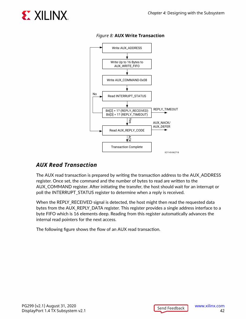
Figure 8: AUX Write Transaction
Write Up to 16 Bytes to AUX_WRITE_FIFO
Write AUX_COMMAND-0x08
Write AUX_ADDRESS
Read INTERRUPT_STATUS
Bit[2] = 1? (REPLY_RECEIVED)Bit[3] = 1? (REPLY_TIMEOUT)
Read AUX_REPLY_CODE
Transaction Complete
No
ACKYes
REPLY_TIMEOUT
AUX_NACK/AUX_DEFER
X21143-062718
AUX Read Transaction
The AUX read transaction is prepared by writing the transaction address to the AUX_ADDRESSregister. Once set, the command and the number of bytes to read are written to theAUX_COMMAND register. After initiating the transfer, the host should wait for an interrupt orpoll the INTERRUPT_STATUS register to determine when a reply is received.
When the REPLY_RECEIVED signal is detected, the host might then read the requested databytes from the AUX_REPLY_DATA register. This register provides a single address interface to abyte FIFO which is 16 elements deep. Reading from this register automatically advances theinternal read pointers for the next access.
The following figure shows the flow of an AUX read transaction.
Chapter 4: Designing with the Subsystem
PG299 (v2.1) August 31, 2020 www.xilinx.comDisplayPort 1.4 TX Subsystem v2.1 42Send Feedback

Figure 9: AUX Read Transaction
Write AUX_COMMAND-0x09
Read INTERRUPT_STATUS Bit[2]
Write AUX_ADDRESS
Bit[2] = 1? (REPLY_RECEIVED)Bit[3] = 1? (REPLY_TIMEOUT)
Read AUX_REPLY_CODE
Read Up to 16 Bytes to AUX_REPLY_DATA
Transaction Complete
No
ACKYes
REPLY_TIMEOUT
AUX_NACK/AUX_DEFER
X21142-062718
AUX Channel Command for I2C TransactionsThe subsystem supports a special AUX channel command intended to make I2C over AUXtransactions faster and easier to perform. In this case, the host bypasses the external I2C master/slave interface and initiates the command by directly writing to the register set.
The sequence for performing these transactions is exactly the same as a native AUX channeltransaction with a change to the command written to the AUX_COMMAND register. Thesupported I2C commands are summarized in the following table.
Table 22: I2C over AUX Commands
AUX_COMMAND[11:8] Command0x0 IIC Write
0x4 IIC Write MOT
0x1 IIC Read
0x5 IIC Read MOT
0x6 IIC Write Status with MOT
0x2 IIC Write Status
By using a combination of these commands, the host can emulate an I2C transaction. Thefollowing figure shows the flow of I2C transactions.
Chapter 4: Designing with the Subsystem
PG299 (v2.1) August 31, 2020 www.xilinx.comDisplayPort 1.4 TX Subsystem v2.1 43Send Feedback

Figure 10: I2C Device Transactions, Write (Left) and Read (Right)
AUX Write Device subaddressIIC_WRITE_MOT
AUX Write Device dataIIC_WRITE_MOT
AUX Write Device addressIIC_WRITE_MOT
Last Byte of Data
AUX Write Device dataIIC_WRITE
Transaction Complete
No
Yes
AUX Write Device subaddressIIC_WRITE_MOT
AUX Read Device addressIIC_READ_MOT
AUX Write Device addressIIC_WRITE_MOT
AUX Read Device dataIIC_READ_MOT
Last Byte of Data
AUX Read Device dataIIC_READ
Transaction Complete
No
Yes
X21141-062718
Because I2C transactions might be significantly slower than AUX channel transactions, the hostshould be prepared to receive multiple AUX_DEFER reply codes during the execution of theabove state machines.
The AUX-I2C commands are as follows:
• MOT Definition:
• Middle Of Transaction bit in the command field.
• This controls the stop condition on the I2C slave.
• For a transaction with MOT set to 1, the I2C bus is not STOPPED, but left to remain theprevious state.
• For a transaction with MOT set to 0, the I2C bus is forced to IDLE at the end of thecurrent command or in special Abort cases.
• Partial ACK: For I2C write transactions, the Sink core can respond with a partial ACK (ACKresponse followed by the number of bytes written to I2C slave).
Special AUX commands include:
• Write Address Only and Read Address Only: These commands do not have any length fieldtransmitted over the AUX channel. The intent of these commands are to:
• Send address and RD/WR information to I2C slave. No Data is transferred.
Chapter 4: Designing with the Subsystem
PG299 (v2.1) August 31, 2020 www.xilinx.comDisplayPort 1.4 TX Subsystem v2.1 44Send Feedback

• End previously active transaction, either normally or through an abort.
The Address Only Write and Read commands are generated from the source by using Bit[12]of the command register with command as I2C WRITE/READ.
• Write Status: This command does not have any length information. The intent of thecommand is to identify the number of bytes of data that have been written to an I2C slavewhen a Partial ACK or Defer response is received by the source on a AUX-I2C write.
The Write status command is generated from the source by using Bit[12] of the commandregister with command as I2C WRITE STATUS.
• IIC Timeout: The Sink controller monitors the IIC bus after a transaction starts and looks foran IIC stop occurrence within 1 second. If an IIC stop is not received, it is considered as an IICtimeout and the sink controller issues a stop condition to release the bus. This timeout avoidsa lock-up scenario.
Generation of AUX Transactions
Generation of AUX transactions are described in the following table.
Set up I2C slave for Write to address defined
Transaction Write Address only with MOT = 11. Write AUX Address register (0x108) with
device address.
2. Issue command to transmit transaction bywriting into AUX command register (0x100).Bit[12] must be set to 1.
AUX Transaction START -> CMD -> ADDRESS -> STOP
I2C Transaction START -> DEVICE_ADDR -> WR -> ACK/NACK
Set up I2C slave for Read to address defined
Transaction Read Address only with MOT = 11. Write AUX Address register with device
address.
2. Issue command to transmit transaction bywriting into AUX command register. Bit [12]must be set to 1.
AUX Transaction START -> CMD -> ADDRESS -> STOP
I2C Transaction START -> DEVICE_ADDR -> RD -> ACK/NACK
To stop the I2C slave, used as Abort or normal stop
Transaction Write/Read Address only with MOT = 01. Write AUX Address register (0x108) with
device address.
2. Issue command to transmit transaction bywriting into AUX command register (0x100).Bit[12] must be set to 1.
AUX Transaction START -> ADDRESS -> STOP
I2C Transaction STOP
Chapter 4: Designing with the Subsystem
PG299 (v2.1) August 31, 2020 www.xilinx.comDisplayPort 1.4 TX Subsystem v2.1 45Send Feedback
Set up I2C slave write data
Transaction Write with MOT = 11. Write AUX Address register (0x108) with
device address.
2. Write the data to be transmitted into AUXwrite FIFO register (0x104).
3. Issue write command and data length totransmit transaction by writing into AUXcommand register (0x100). Bits[3:0] representlength field.
AUX Transaction START -> CMD -> ADDRESS -> LENGTH -> D0 to DN-> STOP
I2C Transaction I2C bus is IDLE or New device addressSTART -> START/RS -> DEVICE_ADDR -> WR -> ACK/NACK -> DATA0 -> ACK/NACK to DATAN -> ACK/NACKI2C bus is in Write state and the same deviceaddressDATA0 -> ACK/NACK to DATAN -> ACK/NACK
Set up I2C slave write data and stop the I2C bus after the current transaction
Transaction Write with MOT = 01. Write AUX Address register (0x108) with
device address.
2. Write the data to be transmitted into AUXwrite FIFO register (0x104).
3. Issue write command and data length totransmit transaction by writing into AUXcommand register (0x100). Bits[3:0] representlength field.
AUX Transaction START -> CMD -> ADDRESS -> LENGTH -> D0 to DN-> STOP
I2C Transaction I2C bus is IDLE or Different I2C device addressSTART -> START/RS -> DEVICE_ADDR -> WR -> ACK/NACK -> DATA0 -> ACK/NACK to DATAN -> ACK/NACK -> STOPI2C bus is in Write state and the same I2C deviceaddressDATA0 -> ACK/NACK to DATAN -> ACK/NACK ->STOP
Set up I2C slave read data
Transaction Read with MOT = 11. Write AUX Address register (0x108) with
device address.
2. Issue read command and data length totransmit transaction by writing into AUXcommand register (0x100). Bits[3:0] representthe length field.
AUX Transaction START -> CMD -> ADDRESS -> LENGTH -> STOP
I2C Transaction I2C bus is IDLE or Different I2C device addressSTART -> START/RS -> DEVICE_ADDR -> RD -> ACK/NACK -> DATA0 -> ACK/NACK to DATAN -> ACK/NACKI2C bus is in Write state and the same I2C deviceaddressDATA0 -> ACK/NACK to DATAN -> ACK/NACK
Set up I2C slave read data and stop the I2C bus after the current transaction
Transaction Read with MOT = 01. Write AUX Address register (0x108) with
device address.
2. Issue read command and data length totransmit transaction by writing into AUXcommand register (0x100). Bits[3:0] representthe length field.
AUX Transaction START -> CMD -> ADDRESS -> LENGTH -> D0 to DN-> STOP
I2C Transaction I2C bus is IDLE or Different I2C device addressSTART -> START/RS -> DEVICE_ADDR -> RD -> ACK/NACK -> DATA0 -> ACK/NACK to DATAN -> ACK/NACK -> STOPI2C bus is in Write state and the same I2C deviceaddressDATA0 -> ACK/NACK to DATAN -> ACK/NACK ->STOP
Status of previous write command that was deferred or partially ACKED
Transaction Write Status with MOT = 11. Write AUX Address register (0x108) with
device address.
2. Issue status update command to transmittransaction by writing into AUX commandregister (0x100). Bit[12] must be set to 1.
AUX Transaction START -> CMD -> ADDRESS -> STOP
I2C Transaction No transaction
Chapter 4: Designing with the Subsystem
PG299 (v2.1) August 31, 2020 www.xilinx.comDisplayPort 1.4 TX Subsystem v2.1 46Send Feedback

Status of previous write command that was deferred or partially ACKED. MOT = 0 ensures that the bus returns toIDLE at the end of the burst.
Transaction Write Status with MOT = 01. Write AUX Address register (0x108) with
device address.
2. Issue status update command to transmittransaction by writing into AUX commandregister (0x100). Bit[12] must be set to 1.
AUX Transaction START -> CMD -> ADDRESS -> STOP
I2C Transaction Force a STOP and the end of write burst
Handling I2C Read Defers/Timeout
The Sink core can issue a DEFER response for a burst read to I2C. The following are the actionsthat can be taken by the Source core.
• Issue the same command (previously issued read, with same device address and length) andwait for response. The Sink core on completion of the read from I2C (after multiple defers)should respond with read data.
• Abort the current read using:
○ Read to a different I2C slave
○ Write command
○ Address-only Read or write with MOT = 0.
Handling I2C Write Partial ACK
The sink could issue a partial ACK response for a burst Write to I2C. The following are theactions that can be taken by the Source core:
• Use the Write status command to poll the transfers happening to the I2C. On successfulcompletion, the sink should issue a NACK response to these requests while intermediate oneswill get a partial ACK.
• Issue the same command for a response (previously issued with the same device address,length and data) and wait for a response. On completion of the write to I2C (after multiplepartial ACKs), the Sink core should respond with an ACK.
• Abort the current Write using:
○ Write to a different I2C slave
○ Read command
○ Address-only Read or Write with MOT = 0.
Handling I2C Write Defer/Timeout
The Sink core can issue a Defer response for a burst write to I2C. The following are the actionsthat can be taken by the Source core:
Chapter 4: Designing with the Subsystem
PG299 (v2.1) August 31, 2020 www.xilinx.comDisplayPort 1.4 TX Subsystem v2.1 47Send Feedback

• Use the Write status command to poll the transfers happening to the I2C. On successfulcompletion, the Sink core should issue an ACK response to these requests while intermediateones will get partial ACKs.
• Issue the same command (previously issued with the same device address, length and data)and wait for a response. The Sink core, on completion of the write to I2C (after multipleDefers), should respond with an ACK.
• Abort the current Write using:
○ Write to a different I2C slave
○ Read command
○ Address only Read or Write with MOT = 0.
AUX IO LocationDisplayPort Source can have AUX IO located inside the IP or external to the IP based on the AUXIO location selection through the GUI. The AUX IO type can be uni-directional/bidirectionalwhen the AUX IO is located inside the IP.
Transmitter Audio/Video Clock GenerationThe transmitter clocking architecture supports both the asynchronous and synchronous clockingmodes included in the VESA DisplayPort Standard v1.4. The clocking mode is selected by way ofthe Stream Clock Mode register (MAIN_STREAM_MISC0 Bit[0]). When set to 1, the link andstream clock are synchronous, in which case the MVid and NVid values are a constant. Insynchronous clock mode, the source core uses the MVid and NVid register values programmedby the host processor through the AXI4-Lite interface.
When the Stream Clock Mode register is set to 0, asynchronous clock mode is enabled and therelationship between MVid and NVid is not fixed. In this mode, the Source core transmits a fixedvalue for NVid and the MVid value provided as a part of the clocking interface.
The following figure shows a block diagram of the transmitter clock generation process.
Figure 11: Transmitter Audio/Video Clock Generation
Attribute Generation
External Clock Management
Stream ClockLink Clock
AXI4-Lite Interface
MVid(23:0)
NVid(23:0)AXI4-Lite
To Framing Insertion
X21140-062718
Chapter 4: Designing with the Subsystem
PG299 (v2.1) August 31, 2020 www.xilinx.comDisplayPort 1.4 TX Subsystem v2.1 48Send Feedback

Hot Plug DetectionThe Source device must debounce the incoming HPD signal by sampling the value at an interval> 250 µs. For a pulse width between 500 µs and 1 ms, the Sink device has requested aninterrupt. The interrupt is passed to the host processor through the AXI4-Lite interface.
If HPD signal remains Low for > 2 ms, then the Sink device has been disconnected and the linkshould be shut down. This condition is also passed through the AXI4-Lite interface as aninterrupt. The host processor must properly determine the cause of the interrupt by reading theappropriate DPCD registers and take the appropriate action. For details, see the VESA DisplayPortStandard v1.4.
HPD Event HandlingHPD signaling has three use cases:
• Connection event defined as HPD_EVENT is detected, and the state of the HPD is 1.
• Disconnection event defined as HPD_EVENT is detected, and the state of the HPD is 0.
• HPD IRQ event as captured in the INTERRUPT_STATUS register Bit[0].
The following figure shows the Source core state and basic actions to be taken based on HPDevents.
Chapter 4: Designing with the Subsystem
PG299 (v2.1) August 31, 2020 www.xilinx.comDisplayPort 1.4 TX Subsystem v2.1 49Send Feedback

Figure 12: HPD Event Handling in Source Core
HPD Disconnected (POR State)
HPD Connected(Operational State)
HPD Interrupt(Transition State)
HPD_EVENT and HPD == 1. Initiate Link Training.
HPD_EVENT and HPD == 0. Disable Main Link.
HPD_IRQ and HPD == 1. Check Link Status and retrain if required.
HPD_EVENT = Interrupt Status Register Bit[1]HPD = Interrupt Signal State Register Bit[0]
X21138-062718
Secondary Channel OperationThe current version of the DisplayPort core supports eight-channel Audio. Secondary Channelfeatures from the DisplayPort Standard v1.4 are supported.
The DisplayPort Audio IP core is offered as modules to provide flexibility and freedom to modifythe system as needed. As shown in the following figure, the Audio interface to the DisplayPortcore is defined using an AXI4-Stream interface to improve system design and IP integration.
Figure 13: Audio Data Interface of DisplayPort Source System
DisplayPortSource
s_aud_axis_aclk
s_aud_axis_aresetn
Ingress_tdata[31:0]
Ingress_tid[7:0]
Ingress_tvalid
Ingress_tready
Main Link
**Add prefix “s_axis_audio” for actual signal names.
X21128-062518
32-bit AXI TDATA is formatted as follows:
Chapter 4: Designing with the Subsystem
PG299 (v2.1) August 31, 2020 www.xilinx.comDisplayPort 1.4 TX Subsystem v2.1 50Send Feedback
Control Bits + 24-bit Audio Sample + Preamble
The ingress channel buffer in the DisplayPort core accepts data from the AXI4-Stream interfacebased on buffer availability and audio control programming. A valid transfer takes place whentready and tvalid are asserted as described in the AXI4-Stream protocol. The ingress channelbuffer acts as a holding buffer.
The DisplayPort Source has a fixed secondary packet length [Header = 4 Bytes + 4 Parity Bytes,Payload = 32 Sample Bytes + 8 Parity Bytes]. In a 1-2 channel transmission, the Sourceaccumulates eight audio samples in the internal channel buffer and then sends the packet tomain link.
Multi-Channel Audio
The DisplayPort TX requires Info frame configuration to transmit multi-channel audio. The Infoframe contains the number of channels and its speaker mapping. The AXI4-Stream TID signalshould contain the Audio channel ID along with audio data, based on the number of channelsconfigured.
For multi-stream audio, secondary data packet ID in the Info frame packet should match with thestream ID over the audio AXI4-Stream interface (TID[7:4]).
Audio ManagementThis section contains the procedural tasks required to achieve audio communication.
Programming DisplayPort Source
1. Disable audio by writing 0x00 to the TX_AUDIO_CONTROL register. The disable bit alsoflushes the buffers in the DisplayPort Source and sets the MUTE bit in VB-ID. Xilinx®
recommends following this step when there is a change in video/audio parameters.
2. Write the Audio Info Frame (based on your requirement; this might be optional for somesystems). The Audio Info Frame consists of eight writes. The order of write transactions areimportant and follow the steps in the DisplayPort Audio registers, offset 0x308 (see relatedinformation).
3. Write Channel Count to the TX_AUDIO_CHANNELS register (the value is actual count -1).
4. If the system is using synchronous clocking then write MAUD and NAUD values toTX_AUDIO_MAUD and TX_AUDIO_NAUD registers, respectively.
5. Enable audio by writing 0x01 to TX_AUDIO_CONTROL register.
Related InformationDisplayPort Audio Registers
Chapter 4: Designing with the Subsystem
PG299 (v2.1) August 31, 2020 www.xilinx.comDisplayPort 1.4 TX Subsystem v2.1 51Send Feedback

Re-Programming Source Audio
1. Disable Audio in DisplayPort 1.4 TX core.
2. Wait until Video/Audio clock is recovered and stable.
3. Enable Audio in DisplayPort 1.4 TX core.
Info Packet Management
The core provides an option to program a single Info packet. The packet is transmitted to the Sinkonce per every video frame or 8192 cycles.
To change an Info packet during transmission, follow these steps:
1. Disable Audio (because a new Info packet means a new audio configuration). The disableaudio also flushes the internal audio buffers.
2. To programm the DisplayPort Source, see Programming the DisplayPort Source.
Related InformationProgramming DisplayPort Source
Extension Packet Management
A single packet buffer is provided for the extension packet. If the extension packet is available inthe buffer, the packet is transmitted as soon as there is availability in the secondary channel. Thepacket length is FIXED to eight words (32 bytes). For VSC Ext packet to be aligned with theVertical Blanking region, set Bit[12] of 0x1A4 register and then program the packet data.
Use the following steps to write an extended packet in the DisplayPort Source controller:
1. Write nine words (as required) into TX_AUDIO_EXT_DATA buffer.
2. Wait for EXT_PKT_TXD interrupt.
3. Write new packet (follow step 1).
Audio Clocking (Recommendation)
The system should have a clock generator (preferably programmable) to generate 512 × fs (AudioSample Rate) clock frequency. The same clock (aud_clk) is used by the DisplayPort Sourcedevice to calculate MAUD and NAUD when running in asynchronous clocking mode.
Chapter 4: Designing with the Subsystem
PG299 (v2.1) August 31, 2020 www.xilinx.comDisplayPort 1.4 TX Subsystem v2.1 52Send Feedback

Figure 14: Audio Clocking for Source
Audio Ingress Interface DisplayPort Source
Audio Clock
512 × fs (Audio Sample Rate)
aud_clk
Main Link
X21136-062718
Note: This should be > 512 × fs
Programming the Core in MST ModeThe section details the steps to program the core in MST mode.
Enabling MST
The following steps are recommended to enable MST functionality:
1. Bring up the main link by following training procedure.
2. Send side band messages using the AUX channel to discover the link (how many downstreamnodes are connected and their capabilities).
3. Enable MST by writing 1 to bit 0 of the MST Config register.
4. Discover MST downstream devices as recommended in section 1.2.1 in the VESA DisplayPortStandard (VESA website).
5. Allocate timeslots based on configuration and the Sink Payload Bandwidth Number (PBN).Typical sideband messages used before VC Payload allocation are Link Address Request,Clear Payload Table, and Enumerate Path Resources.
a. Program VC Payload Buffer 12’h0x800 onwards as per allocation requirement.
b. Program the Sink core with the same allocation timeslots using AUX channel as describedin section 2.6.4 in the DisplayPort Standard.
c. Wait until Sink accepts allocation programming (check DPCD reads to monitor status).
d. After Sink sets VC Payload Allocated (DPCD Address = 0x02C0), set VC PayloadAllocated bit in MST Config register (12’h0x0D0). This enables the source controller tosend an ACT trigger.
6. Wait until ACT Handled bit is set in DPCD Address (0x02C0).
7. Program Video attributes for required streams. Program user pixel width to 4 for all thestreams.
Chapter 4: Designing with the Subsystem
PG299 (v2.1) August 31, 2020 www.xilinx.comDisplayPort 1.4 TX Subsystem v2.1 53Send Feedback

8. Program Rate Governing registers 0x1D0, 0x1D4, 0x1D8, and 0x1DC based on the streamrequirement.
• Program TRANSFER UNIT Size = # of timeslots allocated for that stream. (VC payload sizesource)
• Program FRAC_BYTES_PER_TU = TS_FRAC
• Program MIN_BYTES_PER_TU = TS_INT
• Program INIT_WAIT = 0
Note: Note: Repeat Step 7 for each steam.
9. Enable MST by writing 1 to bit 0 of MST Config register.
Payload Bandwidth Management
The following steps manage payload bandwidth in the source controller.
1. Calculate Target_Average_StreamSymbolTimeSlotsPerMTP based on the VESA DisplayPortStandard (VESA website). Program the VC payload size with the calculatedTarget_Average_StreamSymbolTimeSlotsPerMTP and align it with nearest even boundary.
For example if the value is 13, program the VC payload size for this particular stream to 14.
2. The VC payload calculation for (1920x2200) stream, RGB color sampling, 8 Bits Per Color at5.4 Gb/s, 4 lanes is shown here:
VC Payload Band width = LINK_RATE × Lane_count × 100 (Table 2-136 in the DisplayPortstandard) = 5.4 × 4 × 100 = 2160
Average Stream symbol Time slot per MTP = (Pixel_rate × Bits_per_pixel/8/VC Payload_Bandwidth) × 64 (Section 2.6.4.3.1 in the DisplayPort standard) = (297 MHz × 24 /8/2160) × 64 =26.4
VC Payload Size = 2/4 symbol aligned of (Average Stream symbol Time slot per MTP) = 28
3. Program the VC Payload table as defined in DPCD standard.
4. Program the VC Payload table in source controller as defined in registers 12’h0x800 –12’h0x8FC.
EDID I2C Speed ControlEDID I2C speed can be controlled by programming the I2C Speed Control DPCD register(0x00109) and DisplayPort subsystem supports up to 1 Mb/s I2C speed.
Chapter 4: Designing with the Subsystem
PG299 (v2.1) August 31, 2020 www.xilinx.comDisplayPort 1.4 TX Subsystem v2.1 54Send Feedback

eDP SupportThe DisplayPort TX Subsystem supports the following eDP features:
• Reduced Aux timing
• Alternate Scrambler Seed Reset (ASSR)
• Enhanced Framing
eDP can be enabled by using the following tcl command:
set_property -dict [list CONFIG.EDP_ENABLE {true}] [get_bd_cells v_dp_txss1_0]
Pixel MappingPixel Mapping on AXI4-Stream InterfaceBy default, the pixel mode is selected based on Pixel Frequency in the subsystem driver. Thefollowing shows the different pixel per clock (PPC) for each pixel frequency:
• For 1 PPC, Pixel Frequency < 75 MHz
• For 2 PPC, Pixel Frequency ≥ 75 and < 300 MHz
• For 4 PPC, Pixel Frequency ≥ 300 MHz
Note: 4PPC (QUAD pixel interface) requires 4 lanes, 2PPC (DUAL pixel interface) requires 2 lanes minimum.For more information on the relationship between PPC and lanes, see the description of offset address0x1B8 in Table 18: Main Stream Attributes.
You can override the pixel width dynamically. For example, if the driver selects a 2 pixel mode asdefault, you can change the pixel mode to 1.
• For a pixel mode of 1, valid pixels are available only in pixel 0 position.
• For a pixel mode of 2, valid pixels are available only in pixel 0 and pixel 1 position.
• For a pixel mode of 4, valid pixels are available only in pixel 0, pixel 1, pixel 2, and pixel 3position.
The data width of the AXI4-Stream interface depends on different parameters of the core.
For RGB and YCBCR 4:4:4:4 format Pixel_Width = MAX_BPC × 3 for 4:2:2 formatPixel_Width = MAX_BPC × 2 and for Y-only Pixel_Width = MAX_BPC.
Chapter 4: Designing with the Subsystem
PG299 (v2.1) August 31, 2020 www.xilinx.comDisplayPort 1.4 TX Subsystem v2.1 55Send Feedback
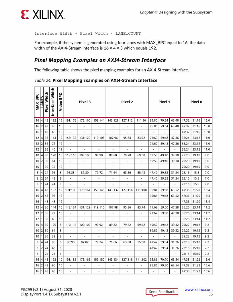
Interface Width = Pixel Width × LANE_COUNT
For example, if the system is generated using four lanes with MAX_BPC equal to 16, the datawidth of the AXI4-Stream interface is 16 × 4 × 3 which equals 192.
Pixel Mapping Examples on AXI4-Stream Interface
The following table shows the pixel mapping examples for an AXI4-Stream interface.
Table 24: Pixel Mapping Examples on AXI4-Stream Interface
MAX
_BPC
LAN
ESPi
xel W
idth
Inte
rfac
e W
idth
Vide
o BP
C
Pixel 3 Pixel 2 Pixel 1 Pixel 0
16 4 48 192 16 191:176 175:160 159:144 143:128 127:112 111:96 95:80 79:64 63:48 47:32 31:16 15:0
16 2 48 96 16 - - - - - - 95:80 79:64 63:48 47:32 31:16 15:0
16 1 48 48 16 - - - - - - - - - 47:32 31:16 15:0
12 4 36 144 12 143:132 131:120 119:108 107:96 95:84 83:72 71:60 59:48 47:36 35:24 23:12 11:0
12 2 36 72 12 - - - - - - 71:60 59:48 47:36 35:24 23:12 11:0
12 1 36 40 12 - - - - - - - - - 35:24 23:12 11:0
10 4 30 120 10 119:110 109:100 99:90 89:80 79:70 69:60 59:50 49:40 39:30 29:20 19:10 9:0
10 2 30 64 10 - - - - - - 59:50 49:40 39:30 29:20 19:10 9:0
10 1 30 32 10 - - - - - - - - - 29:20 19:10 9:0
8 4 24 96 8 95:88 87:80 79:72 71:64 63:56 55:48 47:40 39:32 31:24 23:16 15:8 7:0
8 2 24 48 8 - - - - - - 47:40 39:32 31:24 23:16 15:8 7:0
8 1 24 24 8 - - - - - - - - - 23:16 15:8 7:0
16 4 48 192 12 191:180 175:164 159:148 143:132 127:116 111:100 95:84 79:68 63:52 47:36 31:20 15:4
16 2 48 96 12 - - - - - - 95:84 79:68 63:52 47:36 31:20 15:4
16 1 48 48 12 - - - - - - - - - 47:36 31:20 15:4
12 4 36 144 10 143:134 131:122 119:110 107:98 95:86 83:74 71:62 59:50 47:38 35:26 23:14 11:2
12 2 36 72 10 - - - - - - 71:62 59:50 47:38 35:26 23:14 11:2
12 1 36 40 10 - - - - - - - - - 35:26 23:14 11:2
10 4 30 120 8 119:112 109:102 99:92 89:82 79:72 69:62 59:52 49:42 39:32 29:22 19:12 9:2
10 2 30 64 8 - - - - - - 59:52 49:42 39:32 29:22 19:12 9:2
10 1 30 32 8 - - - - - - - - - 29:22 19:12 9:2
8 4 24 96 6 95:90 87:82 79:74 71:66 63:58 55:50 47:42 39:34 31:26 23:18 15:10 7:2
8 2 24 48 6 - - - - - - 47:42 39:34 31:26 23:18 15:10 7:2
8 1 24 24 6 - - - - - - - - - 23:18 15:10 7:2
16 4 48 192 10 191:182 175:166 159:150 143:134 127:118 111:102 95:86 79:70 63:54 47:38 31:22 15:6
16 2 48 96 10 - - - - - - 95:86 79:70 63:54 47:38 31:22 15:6
16 1 48 48 10 - - - - - - - - - 47:38 31:22 15:6
Chapter 4: Designing with the Subsystem
PG299 (v2.1) August 31, 2020 www.xilinx.comDisplayPort 1.4 TX Subsystem v2.1 56Send Feedback

Table 24: Pixel Mapping Examples on AXI4-Stream Interface (cont'd)M
AX_B
PCLA
NES
Pixe
l Wid
thIn
terf
ace
Wid
th
Vide
o BP
CPixel 3 Pixel 2 Pixel 1 Pixel 0
12 4 36 144 8 143:136 131:124 119:112 107:100 95:88 83:76 71:64 59:52 47:40 35:28 23:16 11:4
12 2 36 72 8 - - - - - - 71:64 59:52 47:40 35:28 23:16 11:4
12 1 36 40 8 - - - - - - - - - 35:28 23:16 11:4
10 4 30 120 6 119:114 109:104 99:94 89:84 79:74 69:64 59:54 49:44 39:34 29:24 19:14 9:4
10 2 30 64 6 - - - - - - 59:54 49:44 39:34 29:24 19:14 9:4
10 1 30 32 6 - - - - - - - - - 29:24 19:14 9:4
16 4 48 192 8 191:184 175:168 159:152 143:136 127:120 111:104 95:88 79:72 63:56 47:40 31:24 15:8
16 2 48 96 8 - - - - - - 95:88 79:72 63:56 47:40 31:24 15:8
16 1 48 48 8 - - - - - - - - - 47:40 31:24 15:8
12 4 36 144 6 143:138 131:126 119:114 107:102 95:90 83:78 71:66 59:54 47:42 35:30 23:18 11:6
12 2 36 72 6 - - - - - - 71:66 59:54 47:42 35:30 23:18 11:6
12 1 36 36 6 - - - - - - - - - 35:30 23:18 11:6
16 4 48 192 6 191:186 175:170 159:154 143:138 127:122 111:106 95:90 79:74 63:58 47:42 31:26 15:10
16 2 48 96 6 - - - - - - 95:90 79:74 63:58 47:42 31:26 15:10
16 1 48 48 6 - - - - - - - - - 47:42 31:26 15:10
Notes:1. The padding bits are zeros.
Pixel Mapping Examples on AXI4-Stream Interface (UG934-Compliant)
The following table shows the pixel mapping examples for an AXI4-Stream interface that isUG934-compliant.
Chapter 4: Designing with the Subsystem
PG299 (v2.1) August 31, 2020 www.xilinx.comDisplayPort 1.4 TX Subsystem v2.1 57Send Feedback
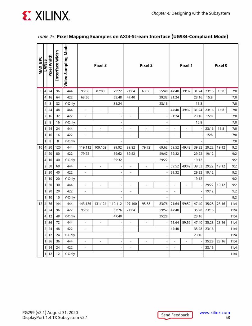
Table 25: Pixel Mapping Examples on AXI4-Stream Interface (UG934-Compliant Mode)M
AX_B
PCLA
NES
Pixe
l Wid
thIn
terf
ace
Wid
th
Vide
o Sa
mpl
ing
Mod
ePixel 3 Pixel 2 Pixel 1 Pixel 0
8 4 24 96 444 95:88 87:80 79:72 71:64 63:56 55:48 47:40 39:32 31:24 23:16 15:8 7:0
4 16 64 422 63:56 55:48 47:40 39:32 31:24 23:16 15:8 7:0
4 8 32 Y-Only 31:24 23:16 15:8 7:0
2 24 48 444 - - - - - - 47:40 39:32 31:24 23:16 15:8 7:0
2 16 32 422 - - - - 31:24 23:16 15:8 7:0
2 8 16 Y-Only - - 15:8 7:0
1 24 24 444 - - - - - - - - - 23:16 15:8 7:0
1 16 16 422 - - - - - - 15:8 7:0
1 8 8 Y-Only - - - 7:0
10 4 30 120 444 119:112 109:102 99:92 89:82 79:72 69:62 59:52 49:42 39:32 29:22 19:12 9:2
4 20 80 422 79:72 69:62 59:52 49:42 39:32 29:22 19:12 9:2
4 10 40 Y-Only 39:32 29:22 19:12 9:2
2 30 60 444 - - - - - - 59:52 49:42 39:32 29:22 19:12 9:2
2 20 40 422 - - - - 39:32 29:22 19:12 9:2
2 10 20 Y-Only - - 19:12 9:2
1 30 30 444 - - - - - - - - - 29:22 19:12 9:2
1 20 20 422 - - - - - - 19:12 9.2
1 10 10 Y-Only - - - 9:2
12 4 36 144 444 143:136 131:124 119:112 107:100 95:88 83:76 71:64 59:52 47:40 35:28 23:16 11:4
4 24 96 422 95:88 83:76 71:64 59:52 47:40 35:28 23:16 11:4
4 12 48 Y-Only 47:40 35:28 23:16 11:4
2 36 72 444 - - - - - - 71:64 59:52 47:40 35:28 23:16 11:4
2 24 48 422 - - - - 47:40 35:28 23:16 11:4
2 12 24 Y-Only - - 23:16 11:4
1 36 36 444 - - - - - - - - - 35:28 23:16 11:4
1 24 24 422 - - - - - - 23:16 11:4
1 12 12 Y-Only - - - 11:4
Chapter 4: Designing with the Subsystem
PG299 (v2.1) August 31, 2020 www.xilinx.comDisplayPort 1.4 TX Subsystem v2.1 58Send Feedback

Table 25: Pixel Mapping Examples on AXI4-Stream Interface (UG934-Compliant Mode)(cont'd)
MAX
_BPC
LAN
ESPi
xel W
idth
Inte
rfac
e W
idth
Vide
o Sa
mpl
ing
Mod
ePixel 3 Pixel 2 Pixel 1 Pixel 0
16 4 48 192 444 191:184 175:168 159:152 143:136 127:120 111:104 95:88 79:72 63:56 47:40 31:24 15:8
4 32 128 422 127:120 111:104 95:88 79:72 63:56 47:40 31:24 15:8
4 16 64 Y-Only 63:56 47:40 31:24 15:8
2 48 96 444 - - - - - - 95:88 79:72 63:56 47:40 31:24 15:8
2 32 64 422 - - - - 63:56 47:40 31:24 15:8
2 16 32 Y-Only - - 31:24 15:8
1 48 48 444 - - - - - - - - - 47:40 31:24 15:8
1 32 32 422 - - - - - - 31:24 15:8
1 16 16 Y-Only - - - 15:8
Notes:1. Video BPC is 8.
Pixel Mapping on Native Video InterfaceThe primary interface for user image data has been modeled on the industry standard for displaytiming controller signals. The port list consists of video timing information encoded in a verticaland horizontal sync pulse and data valid indicator. These single bit control lines frame the activedata and provide flow control for the AXI4-Stream video.
Vertical timing is framed using the vertical sync pulse which indicates the end of frame N - 1 andthe beginning of frame N. The vertical back porch is defined as the number of horizontal syncpulses between the end of the vertical sync pulse and the first line containing active pixel data.The vertical front porch is defined as the number of horizontal sync pulses between the last lineof active pixel data and the start of the vertical sync pulse. When combined with the verticalback porch and the vertical sync pulse width, these parameters form what is commonly known asthe vertical blanking interval.
At the trailing edge of each vertical sync pulse, the user data interface resets key elements of theimage datapath. This provides for a robust user interface that recovers from any kind of interfaceerror in one vertical interval or less.
The following figure shows the typical signaling of a full frame of data.
Chapter 4: Designing with the Subsystem
PG299 (v2.1) August 31, 2020 www.xilinx.comDisplayPort 1.4 TX Subsystem v2.1 59Send Feedback

Figure 15: User Interface Vertical Timing
Vertical Sync
Horizontal Sync
Data Valid
Vertical Sync Width
Vertical Back Porch
Vertical Front PorchVertical Resolution
X21145-062718
Similarly, the horizontal timing information is defined by a front porch, back porch, and pulsewidth. The porch values are defined as the number of clocks between the horizontal sync pulseand the start or end of active data. Pixel data is only accepted into the image data interface whenthe data valid flag is active-High. The following figure is an enlarged version of the previousfigure, giving more details on a single scan line. The horizontal sync pulse should be used as a lineadvance signal. Use the rising edge of this signal to increment the line count.
Note: Data Valid might toggle if using a fast clock. Also, Data Valid signal might remain asserted for theduration of a scan line. Dropping the valid signal might result in improper operation.
Figure 16: User Interface Horizontal Timing
HorizontalFront Porch
Horizontal Sync
Data Valid
HorizontalBack Porch
Horizontal Resolution
X16350-062518
In the two-dimensional image plane, these control signals frame a rectangular region of activepixel data within the total frame size. This relationship of the total frame size to the active framesize is shown in here.
Chapter 4: Designing with the Subsystem
PG299 (v2.1) August 31, 2020 www.xilinx.comDisplayPort 1.4 TX Subsystem v2.1 60Send Feedback

Figure 17: Active Image Data
Active Image
X21147-062718
The User Data interface can accept one, two, or four pixels per clock cycle. The vid_pixelwidth is always 48-bits, regardless if all bits are used. For pixel mappings that do not require all48 bits, the convention used for this core is to occupy the MSB bits first and leave the lower bitseither untied or driven to zero.
Pixel Mapping Examples on the User Data Interface
The following table shows the correct mapping for all supported data formats.
Table 26: Pixel Mapping Examples on the User Data Interface
Format BPC/BPP R G B Cr Y Cb Cr/Cb YRGB 6/18 [47:42] [31:26] [15:10] - - - - -
RGB 8/24 [47:40] [31:24] [15:8] - - - - -
RGB 10/30 [47:38] [31:22] [15:6] - - - - -
RGB 12/36 [47:36] [31:20] [15:4] - - - - -
RGB 16/48 [47:32] [31:16] [15:0] - - - - -
YCrCb444 6/18 - - - [47:42] [31:26] [15:10] - -
YCrCb444 8/24 - - - [47:40] [31:24] [15:8] - -
YCrCb444 10/30 - - - [47:38] [31:22] [15:6] - -
YCrCb444 12/36 - - - [47:36] [31:20] [15:4] - -
YCrCb444 16/48 - - - [47:32] [31:16] [15:0] - -
YCrCb422 8/16 - - - - - - [47:40] [31:24]
YCrCb422 10/20 - - - - - - [47:38] [31:22]
YCrCb422 12/24 - - - - - - [47:36] [31:20]
YCrCb422 16/32 - - - - - - [47:32] [31:16]
YONLY 8/8 - - - - - - - [47:40]
YONLY 10/10 - - - - - - - [47:38]
YONLY 12/12 - - - - - - - [47:36]
Chapter 4: Designing with the Subsystem
PG299 (v2.1) August 31, 2020 www.xilinx.comDisplayPort 1.4 TX Subsystem v2.1 61Send Feedback

Table 26: Pixel Mapping Examples on the User Data Interface (cont'd)
Format BPC/BPP R G B Cr Y Cb Cr/Cb YYONLY 16/16 - - - - - - - [47:32]
Notes:1. For a YCrCb 4:2:2, the input follows YCr, YCb, YCr, YCb, and so on. This means Cr and Cb are mapped to the same bits
on the video input ports of the source core. The source core expects YCb first, followed by YCr.
Selecting the Pixel Interface
To determine the necessary pixel interface to support a specific resolution, it is important toknow the active resolution and blanking information.
Note: In a quad pixel interface, if the resolution is not divisible by four, you should add zeros at the end offrame, over the video interface pixel data.
For example, to support an active resolution of 2560 × 1600 @ 60, there are two possibleblanking formats: Normal Blanking and Reduced Blanking, as defined by the VESA standard.
2560 × 1600 @ 60 + Blanking = 3504 × 1658 @ 60 requires a pixel clock of 348.58 MHz
2560 × 1600 @ 60 + Reduced Blanking = 2720 × 1646 @ 60 requires a Pixel clock of268.63 MHz
Assuming a pixel clock of 150 MHz and a dual pixel interface:
2560 × 1600 @ 60 + Blanking = 3504 × 1658 @ 60 = 348.58 MHz
348.58 MHz / 2 = 172.28 MHz
2560 × 1600 @ 60 + Reduced Blanking = 2720 × 1646 @ 60 = 268.63 MHz
268.63 MHz / 2 = 134.31 MHz
With a dual pixel interface, the DisplayPort 1.4 TX Subsystem IP can support 2560 × 1600 only ifthere is a Reduced Blanking input. If full Blanking support is needed, then a four pixel interfaceshould be used.
The following figures show timing diagrams for the three pixel interface options.
Figure 18: Single Pixel Timing
X21131-091818
Chapter 4: Designing with the Subsystem
PG299 (v2.1) August 31, 2020 www.xilinx.comDisplayPort 1.4 TX Subsystem v2.1 62Send Feedback

Figure 19: Dual Pixel Timing
X21572-091818
Figure 20: Quad Pixel Timing
X21573-091818
AXI4-Stream Interface Color MappingThis table shows the color mapping for the AXI4-Stream interface and this complies with theguidelines in the AXI4-Stream Video IP and System Design Guide (UG934).
Table 27: AXI4-Stream Interface Data Mapping
AXI4-Stream InterfacePixel 3 Pixel 2 Pixel 1 Pixel 0
Com
p3
Com
p2
Com
p1
Com
p3
Com
p2
Com
p1
Com
p3
Com
p2
Com
p1
Com
p3
Com
p2
Com
p1
RGB R B G R B G R B G R B G
YCbCr444 Cr Cb Y Cr Cb Y Cr Cb Y Cr Cb Y
YCbCr422 - Cr/Cb Y - Cr/Cb Y - Cr/Cb Y - Cr/Cb Y
Y-Only - - Y - - Y - - Y - - Y
Notes:1. For component widths, see the Pixel Mapping Examples on AXI4-Stream Interface.
Related InformationPixel Mapping Examples on AXI4-Stream Interface
Chapter 4: Designing with the Subsystem
PG299 (v2.1) August 31, 2020 www.xilinx.comDisplayPort 1.4 TX Subsystem v2.1 63Send Feedback

ClockingThis section describes the link clock (tx_lnk_clk) and the video clock(tx_vid_clk_stream1). The AXI4-Stream to Video Bridge can handle asynchronous clocking.The value is based on the Consumer Electronics Association (CEA)/VESA Display Monitor Timing(DMT) standard for given video resolutions.
The tx_lnk_clk is a link clock input to the DisplayPort 1.4 TX Subsystem generated by theVideo PHY (GT). The frequency of tx_lnk_clk is <line_rate>/20 MHz for 16-bit interface.
The hdcp_ext_clk input can be driven from external MMCM or BUFGCDIV where it has afrequency requirement of hdcp_ext_clk = tx_lnk_clk/2 MHz.
In both, native and AXI4-stream modes TX video clock value is based on the ConsumerElectronics Association (CEA)/VESA Display Monitor Timing (DMT) standard for given videoresolutions.
The core uses six clock domains:
• lnk_clk: The txoutclk from the Video PHY is connected to the TX subsystem link clock.Most of the core operates in the link clock domain. This domain is based on thelnk_clk_p/n reference clock for the transceivers. The link rate switching is handled by aDRP state machine in the core PHY later. When the lanes are running at 2.7 Gb/s, lnk_clkoperates at 135 MHz. When the lanes are running at 1.62 Gb/s, lnk_clk operates at 81MHz. When the lanes are running at 5.4 Gb/s, lnk_clk operates at 270 MHz.When the lanesare running at 8.1 Gb/s, lnk_clk operates at 405 MHz.
Note: lnk_clk = link_rate/20, when the GT data width is 16 bits.
• vid_clk: This is the primary user interface clock. It is based on the DisplayPort Standard, thevideo clock can be derived from the link clock using mvid and nvid.In addition, vid_clkshould be at least [(Vtotal x Htotal x frames per second)/pixels per clock]
• s_axi_aclk: This is the processor domain. It has been tested to run as fast as 135 MHz. TheAUX clock domain is derived from this domain, but requires no additional constraints. InUltraScale™ FPGA, s_axi_aclk clock is connected to a free-running clock input.gtwiz_reset_clk_freerun_in is required by the reset controller helper block to resetthe transceiver primitives. A new GUI parameter is added for AXI_Frequency, when theDisplayPort IP is targeted to UltraScale FPGA. The requirement is s_axi_aclk ≤ lnk_clk.
• aud_clk: This is the audio interface clock. The frequency will be equal to 512 × audio samplerate.
• s_aud_axis_aclk: This clock is used by the source audio streaming interface. This clock shouldbe = 512 × audio sample rate.
Chapter 4: Designing with the Subsystem
PG299 (v2.1) August 31, 2020 www.xilinx.comDisplayPort 1.4 TX Subsystem v2.1 64Send Feedback

• m_aud_axis_aclk: This clock is used by the sink audio streaming interface. This clock should be= 512 × audio sample rate.
For more information on clocking, see the Video PHY Controller LogiCORE IP Product Guide(PG230).
ResetsThe subsystem has one reset input for each of the AXI4-Lite, AXI4-Stream, and Video interfaces:
• s_axi_aresetn: Active-Low AXI4-Lite reset. This resets all the programming registers.
• tx_vid_reset_stream1: Active-High video pipe reset. For MST with four streams, there are fourvideo resets.
• s_axis_aresetn_stream1: Active-Low AXI4-Stream interface reset. For MST with four streams,there are four resets corresponding to each stream.
• m_aresetn_stream1: Active-Low reset for streams one and two.
Address Map ExampleThe following table shows an example based on a subsystem base address of 0x44C0_0000 (19bits). The DisplayPort 1.4 TX Subsystem requires a 19-bit address mapping, starting at an offsetaddress of 0x00000.
This address map example is applicable when the TX subsystem is configured in the AXI4-Streaminterface mode.
Table 28: Address Map Example
IP Core/Subsystem SST MSTDisplayPort 1.4 TX Core 0x44C0_0000 0x44C0_0000
VTC 0 0x44C0_1000 0x44C0_1000
VTC 1 (N = 2) N/A 0x44C0_2000
VTC 1 (N = 3) N/A 0x44C0_3000
VTC 1 (N = 4) N/A 0x44C0_4000
HDCP Controller 0x44C0_2000 N/A
AXI Timer 0x44C0_3000 N/A
Chapter 4: Designing with the Subsystem
PG299 (v2.1) August 31, 2020 www.xilinx.comDisplayPort 1.4 TX Subsystem v2.1 65Send Feedback

Chapter 5
Design Flow StepsThis section describes customizing and generating the subsystem, constraining the subsystem,and the simulation, synthesis, and implementation steps that are specific to this IP subsystem.More detailed information about the standard Vivado® design flows and the IP integrator can befound in the following Vivado Design Suite user guides:
• Vivado Design Suite User Guide: Designing IP Subsystems using IP Integrator (UG994)
• Vivado Design Suite User Guide: Designing with IP (UG896)
• Vivado Design Suite User Guide: Getting Started (UG910)
• Vivado Design Suite User Guide: Logic Simulation (UG900)
Customizing and Generating the SubsystemThis section includes information about using Xilinx® tools to customize and generate thesubsystem in the Vivado® Design Suite.
If you are customizing and generating the subsystem in the Vivado IP integrator, see the VivadoDesign Suite User Guide: Designing IP Subsystems using IP Integrator (UG994) for detailedinformation. IP integrator might auto-compute certain configuration values when validating orgenerating the design. To check whether the values do change, see the description of theparameter in this chapter. To view the parameter value, run the validate_bd_designcommand in the Tcl console.
You can customize the IP for use in your design by specifying values for the various parametersassociated with the IP subsystem using the following steps:
1. Select the IP from the IP catalog.
2. Double-click the selected IP or select the Customize IP command from the toolbar or right-click menu.
For details, see the Vivado Design Suite User Guide: Designing with IP (UG896) and the VivadoDesign Suite User Guide: Getting Started (UG910).
Figures in this chapter are illustrations of the Vivado IDE. The layout depicted here might varyfrom the current version.
Chapter 5: Design Flow Steps
PG299 (v2.1) August 31, 2020 www.xilinx.comDisplayPort 1.4 TX Subsystem v2.1 66Send Feedback

Subsystem Configuration ScreenThe subsystem configuration screen is shown in the following figure.
Figure 21: Configuration Screen
• Component Name: The Component Name is used as the name of the top-level wrapper filefor the core. The underlying netlist still retains its original name. Names must begin with aletter and must be composed from the following characters: a through z, 0 through 9, and "_".The name displayport_0 is used as internal module name and should not be used for thecomponent name. The default is v_dp_txss1_0.
• Mode: Selects the desired resolution for the video stream out. Options are SST or MST.
• Video Interface: Selects the AXI4-Streamor native for the input video interface.
• MST Streams: Selects the maximum number of streams in MST mode.
• Lane Count: Selects the maximum number of lanes.
• Bits Per Color: Selects the desired maximum bit per component (BPC).
• Link Rate: Selects the desired link rate in Gb/s.
• Enable HDCP 1.3 Encryption: Enables the HDCP 1.3 encryption.
• Enable HDCP 2.2 Encryption: Enables the HDCP 2.2 encryption.
• Enable Audio: Enables the audio support.
Chapter 5: Design Flow Steps
PG299 (v2.1) August 31, 2020 www.xilinx.comDisplayPort 1.4 TX Subsystem v2.1 67Send Feedback
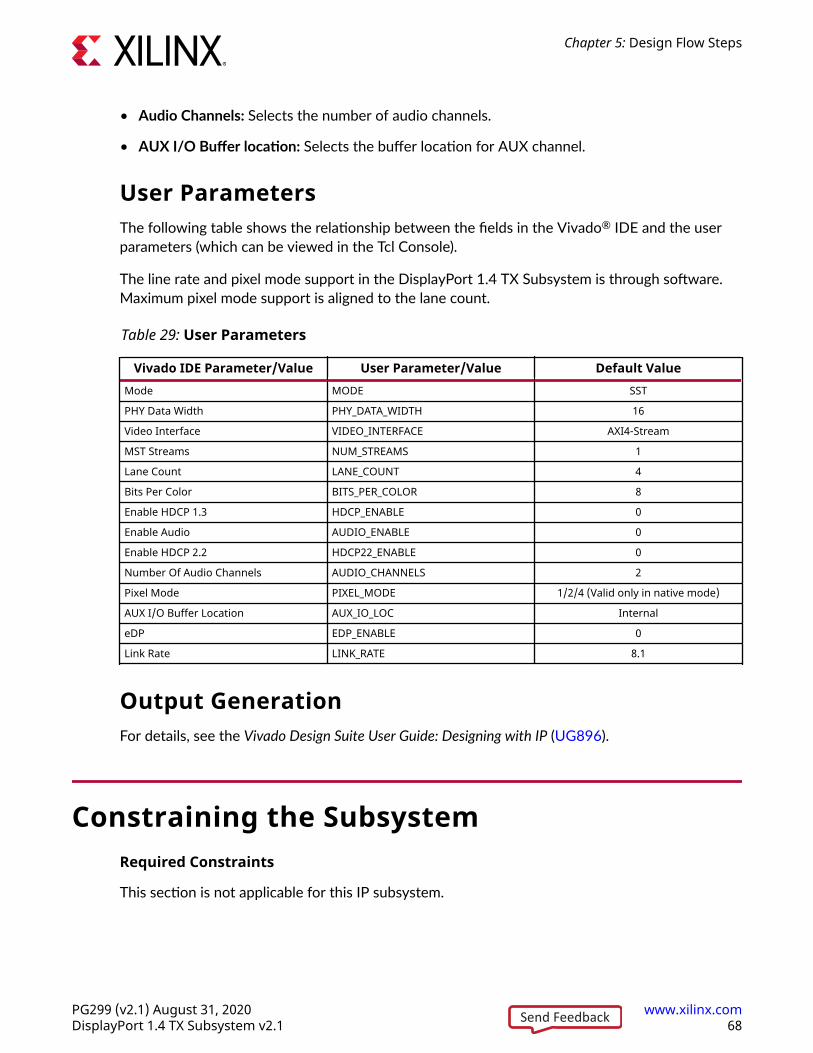
• Audio Channels: Selects the number of audio channels.
• AUX I/O Buffer location: Selects the buffer location for AUX channel.
User ParametersThe following table shows the relationship between the fields in the Vivado® IDE and the userparameters (which can be viewed in the Tcl Console).
The line rate and pixel mode support in the DisplayPort 1.4 TX Subsystem is through software.Maximum pixel mode support is aligned to the lane count.
Table 29: User Parameters
Vivado IDE Parameter/Value User Parameter/Value Default ValueMode MODE SST
PHY Data Width PHY_DATA_WIDTH 16
Video Interface VIDEO_INTERFACE AXI4-Stream
MST Streams NUM_STREAMS 1
Lane Count LANE_COUNT 4
Bits Per Color BITS_PER_COLOR 8
Enable HDCP 1.3 HDCP_ENABLE 0
Enable Audio AUDIO_ENABLE 0
Enable HDCP 2.2 HDCP22_ENABLE 0
Number Of Audio Channels AUDIO_CHANNELS 2
Pixel Mode PIXEL_MODE 1/2/4 (Valid only in native mode)
AUX I/O Buffer Location AUX_IO_LOC Internal
eDP EDP_ENABLE 0
Link Rate LINK_RATE 8.1
Output GenerationFor details, see the Vivado Design Suite User Guide: Designing with IP (UG896).
Constraining the SubsystemRequired Constraints
This section is not applicable for this IP subsystem.
Chapter 5: Design Flow Steps
PG299 (v2.1) August 31, 2020 www.xilinx.comDisplayPort 1.4 TX Subsystem v2.1 68Send Feedback

Device, Package, and Speed Grade Selections
See IP Facts in the related information below for details about supported devices.
This section is not applicable for this IP subsystem.
Clock Frequencies
See Clocking for more details about clock frequencies. For more information on GT clocking, seethe Video PHY Controller LogiCORE IP Product Guide (PG230).
Clock Management
This section is not applicable for this IP subsystem.
Clock Placement
This section is not applicable for this IP subsystem.
Banking
For more information on the specific banking constraints, see the Video PHY Controller LogiCOREIP Product Guide (PG230).
Transceiver Placement
For more information on the specific transceiver placement constraints, see the Video PHYController LogiCORE IP Product Guide (PG230).
I/O Standard and Placement
This section is not applicable for this IP subsystem.
AUX Channel
The VESA DisplayPort Standard (VESA website) describes the AUX channel as a bidirectional LVDSsignal. For , hence there are no specific transceiver placement constraints. For more informationon the specific transceiver placement constraints, see the 7 series designs, the core usesIOBUFDS (bidirectional buffer) as the default with the LVDS standard. You should design theboard as recommended by the VESA DP Protocol Standard. For reference, see the exampledesign XDC file.
For UltraScale+™ and UltraScale™ families supporting HR IO banks, use the following Sourceconstraints:
set_property IOSTANDARD LVDS_25 [get_ports aux_tx_io_p]set_property IOSTANDARD LVDS_25 [get_ports aux_tx_io_n]
Chapter 5: Design Flow Steps
PG299 (v2.1) August 31, 2020 www.xilinx.comDisplayPort 1.4 TX Subsystem v2.1 69Send Feedback

For UltraScale+ and UltraScale families supporting HP IO banks, use the following Sourceconstraints:
set_property IOSTANDARD LVDS [get_ports aux_tx_io_p]set_property IOSTANDARD LVDS [get_ports aux_tx_io_n]
HPD
The HPD signal can operate in either a 3.3V or 2.5V I/O bank. By definition in the standard, it is a3.3V signal.
For UltraScale+ and UltraScale families supporting HR IO banks, use the following constraints:
set_property IOSTANDARD LVCMOS25 [get_ports hpd];
For UltraScale+ and UltraScale families supporting HP IO banks, use the following constraints:
set_property IOSTANDARD LVCMOS18 [get_ports hpd];
Board design and connectivity should follow DisplayPort standard recommendations with properlevel shifting.
Related InformationIP FactsClocking
SimulationThere is no simulation support for DisplayPort 1.4 TX Subsystem.
Synthesis and ImplementationFor details about synthesis and implementation, see the Vivado Design Suite User Guide: Designingwith IP (UG896).
Chapter 5: Design Flow Steps
PG299 (v2.1) August 31, 2020 www.xilinx.comDisplayPort 1.4 TX Subsystem v2.1 70Send Feedback

Chapter 6
Example DesignNote: All example designs use the Inrevium TB-FMCH-VFMC-DP FMC card.
This chapter contains step-by-step instructions for generating an Application Example Designfrom the DisplayPort 1.4 TX Subsystem by using the Vivado® Design Suite flow.
RECOMMENDED: For ZCU102/VCU118 (Revision 1.0 or later), you should set up a 1.8V setting afterconnecting the DisplayPort FMC. For details on the FMC voltage, see the Related Information link. For moreinformation, see the ZCU102 System Controller GUI Tutorial (registration required) (XTP433) and the VCU118System Controller Tutorial (registration required) (XTP447).
Related InformationSetting the FMC Voltage to 1.8V
Available Example DesignsThe following table shows the example designs available for the TX and RX DisplayPort 1.4subsystems.
Table 30: Available Example Designs
GTType Topology
Video PHY ConfigHardware BPC Processor
(TXPLL) (RXPLL)GTHE3 Pass-through without
HDCP1.3QPLL CPLL KCU105 +
Inrevium TB-FMCH-VFMC-DP
8 MicroBlaze™
Chapter 6: Example Design
PG299 (v2.1) August 31, 2020 www.xilinx.comDisplayPort 1.4 TX Subsystem v2.1 71Send Feedback

Table 30: Available Example Designs (cont'd)
GTType Topology
Video PHY ConfigHardware BPC Processor
(TXPLL) (RXPLL)GTHE4 RX only - CPLL ZCU102 +
Inrevium TB-FMCH-VFMC-DP
10 A53
TX only QPLL - ZCU102 +Inrevium TB-
FMCH-VFMC-DP
10 A53
FB Pass-through withoutHDCP1.3/HDCP2.2
QPLL CPLL ZCU102 +Inrevium TB-
FMCH-VFMC-DP
10 A53
FB Pass-through withHDCP1.3 and HDCP2.2
QPLL CPLL ZCU102 +Inrevium TB-
FMCH-VFMC-DP
10 A53
MST FB Pass-throughwithout HDCP1.3 and TX only
QPLL CPLL ZCU102+ InreviumTB-FMCH-VFMC-
DP
10 A53
GTYE4 RX only - CPLL VCU118 +Inrevium TB-
FMCH-VFMC-DP
10 MicroBlaze
TX only QPLL - VCU118 +Inrevium TB-
FMCH-VFMC-DP
10 MicroBlaze
Notes:1. GT data width is 2 bytes.
Building the Example Design1. Open the Vivado® Design Suite and click Create Project.
Chapter 6: Example Design
PG299 (v2.1) August 31, 2020 www.xilinx.comDisplayPort 1.4 TX Subsystem v2.1 72Send Feedback

2. In the New Project window, enter a Project name, Project location, and click Next up to theBoard/Part selection window.
3. In the Default Part window, select the Board as per your requirement. Application ExampleDesigns are available for KCU105, ZCU102, and VCU118.
Chapter 6: Example Design
PG299 (v2.1) August 31, 2020 www.xilinx.comDisplayPort 1.4 TX Subsystem v2.1 73Send Feedback
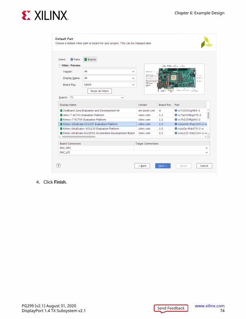
4. Click Finish.
Chapter 6: Example Design
PG299 (v2.1) August 31, 2020 www.xilinx.comDisplayPort 1.4 TX Subsystem v2.1 74Send Feedback

5. In the Flow Navigator window, click Create Block Design (BD). Select a name for the BlockDesign and click OK.
Chapter 6: Example Design
PG299 (v2.1) August 31, 2020 www.xilinx.comDisplayPort 1.4 TX Subsystem v2.1 75Send Feedback

6. Right-click BD and click Add IP. Search for DisplayPort 1.4 and select either the DisplayPort1.4 Receiver Subsystem IP (for RX only (ZCU102, VCU118), Pass-through (KCU105, ZCU102)designs) or the DisplayPort 1.4 Transmitter Subsystem IP (for TX only (ZCU102, VCU118), orPass-through (KCU105) designs).
7. Double-click the IP and go to the Application Example Design tab in the Customize IPwindow. Select the supported topology in the Application Example Design drop-down box.Click OK and Save the block design.
Chapter 6: Example Design
PG299 (v2.1) August 31, 2020 www.xilinx.comDisplayPort 1.4 TX Subsystem v2.1 76Send Feedback

8. Right-click the DisplayPort Subsystem IP under Design source in the Design tab and clickOpen IP Example Design.
9. Choose Example project directory and click OK.
Chapter 6: Example Design
PG299 (v2.1) August 31, 2020 www.xilinx.comDisplayPort 1.4 TX Subsystem v2.1 77Send Feedback

10. The following figure shows the Vivado IP integrator design. Choose the Generate Bitstream.
Chapter 6: Example Design
PG299 (v2.1) August 31, 2020 www.xilinx.comDisplayPort 1.4 TX Subsystem v2.1 78Send Feedback

11. Export the hardware (xsa) to Vitis software platform. Click File → Export → Export Hardware.
12. Launch Vitis software platform from command line. Setup a workspace and create a platformproject using exported xsa.
Chapter 6: Example Design
PG299 (v2.1) August 31, 2020 www.xilinx.comDisplayPort 1.4 TX Subsystem v2.1 79Send Feedback
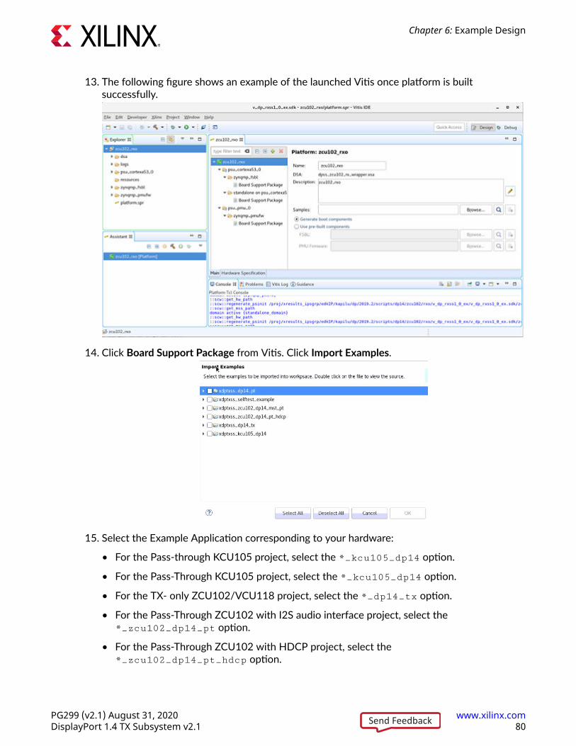
13. The following figure shows an example of the launched Vitis once platform is builtsuccessfully.
14. Click Board Support Package from Vitis. Click Import Examples.
15. Select the Example Application corresponding to your hardware:
• For the Pass-through KCU105 project, select the *_kcu105_dp14 option.
• For the Pass-Through KCU105 project, select the *_kcu105_dp14 option.
• For the TX- only ZCU102/VCU118 project, select the *_dp14_tx option.
• For the Pass-Through ZCU102 with I2S audio interface project, select the*_zcu102_dp14_pt option.
• For the Pass-Through ZCU102 with HDCP project, select the*_zcu102_dp14_pt_hdcp option.
Chapter 6: Example Design
PG299 (v2.1) August 31, 2020 www.xilinx.comDisplayPort 1.4 TX Subsystem v2.1 80Send Feedback

• For the MST FB Pass-Through ZCU102 project, select the *_zcu102_dp14_mst_ptoption.
• For the Passthrough ZCU102 with I2S audio interface project, select the*_zcu102_dp14_pt option.
• For the Passthrough ZCU102 with HDCP project, select the *_zcu102_dp14_pt_hdcpoption.
• For the MST FB Pass-through ZCU102 project, select the *_zcu102_dp14_mst_ptoption.
16. Build the example in Vitis software platform by right clicking and selecting Build Project.
Hardware Setup and Run1. Connect the Tokyo Electron Device Limited (TED) TB-FMCH-VFMC-DP module to the HPC
FMC connector on the KCU105 board or to the HPC0 connector on the ZCU102 or to theFMCP HSPC connector on the VCU118 depending on your design.
2. Connect a USB cable (Type A to mini B) from the host PC to the USB UART port on theKCU105 for serial communication. For the KCU105, ZCU102, or VCU118, use Type A tomicro B type of USB cable.
3. Connect a JTAG USB Platform cable or a USB Type A to Micro B cable from the host PC tothe board for programming bit and elf files.
4. For pass-through or TX-only applications, connect a DP cable from the TX port of the TEDTB-FMCH-VFMC-DP module to a monitor, as shown in the following figure.
Chapter 6: Example Design
PG299 (v2.1) August 31, 2020 www.xilinx.comDisplayPort 1.4 TX Subsystem v2.1 81Send Feedback

5. For pass-through or RX-only applications, connect a DP cable from the RX port of the TEDTB-FMCH-VFMC-DP module to a DP source (GPU), as shown in the following figure.
Figure 22: KCU105 Board Setup
Chapter 6: Example Design
PG299 (v2.1) August 31, 2020 www.xilinx.comDisplayPort 1.4 TX Subsystem v2.1 82Send Feedback

Figure 23: ZCU102 Board Setup
6. On the KCU105 set the mode pin to SW15:
SW15
1 2 3 4 5 6
X20381-062518
7. On the ZCU102 set the mode pin to SW6:
SW6
1 2 3 4X19805-062518
8. Connect the power supply and power on the board.
Chapter 6: Example Design
PG299 (v2.1) August 31, 2020 www.xilinx.comDisplayPort 1.4 TX Subsystem v2.1 83Send Feedback
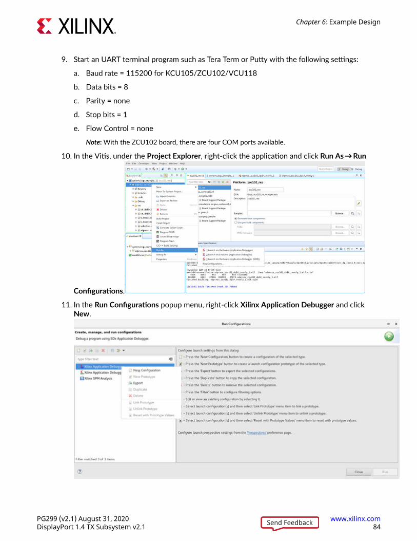
9. Start an UART terminal program such as Tera Term or Putty with the following settings:
a. Baud rate = 115200 for KCU105/ZCU102/VCU118
b. Data bits = 8
c. Parity = none
d. Stop bits = 1
e. Flow Control = none
Note: With the ZCU102 board, there are four COM ports available.
10. In the Vitis, under the Project Explorer, right-click the application and click Run As → Run
Configurations.
11. In the Run Configurations popup menu, right-click Xilinx Application Debugger and clickNew.
Chapter 6: Example Design
PG299 (v2.1) August 31, 2020 www.xilinx.comDisplayPort 1.4 TX Subsystem v2.1 84Send Feedback

12. In the Target Setup tab, the Reset entire system is enabled.
13. In the Application tab click Run.
Chapter 6: Example Design
PG299 (v2.1) August 31, 2020 www.xilinx.comDisplayPort 1.4 TX Subsystem v2.1 85Send Feedback

Display User ConsoleIn a Pass-Through application (KCU105), as soon as the application is executed, it checks if aMonitor is connected or not. If a monitor is already connected, then it starts up the followingoptions as shown in the following figure to choose from (KCU105).
Figure 24: DisplayPort User Console
Selecting either r or s puts the system in Pass-Through mode, where the video received by theRX is forwarded to the TX. This configures the vid_phy_controller and sets up theDisplayPort for RX. If a DisplayPort Source (for example, GPU) is already connected toDisplayPort RX Subsystem, then it starts the training. Otherwise, the training starts when thecable is plugged in. As soon as the training is completed, the application starts the DisplayPort TXSubsystem. The video should be seen on the monitor after the TX is up. The previous figureshows the UART transcript. The transcript might differ based on the training done by the GPU.
Chapter 6: Example Design
PG299 (v2.1) August 31, 2020 www.xilinx.comDisplayPort 1.4 TX Subsystem v2.1 86Send Feedback

Setting the FMC Voltage to 1.8VTo run the example design on the ZCU102/VCU118 board, ensure that only one ZCU102/VCU118 board is connected to the host PC. This tool does not work with multiple ZCU102/VCU118 connected to the host PC. There is no UART selection in this tool. Also, the FMCvoltage is set to 1.8V. If you forget to set the FMC voltage, the following symptoms might occur:
• Random AUX failures
• Training failures
To set the FMC VADJ voltage:
1. Connect the ZCU102/VCU118 board from the host PC to the USB UART port and power upthe board.
2. Open the ZCU102/VCU118 SCUI tool and select the FMC tab.
3. On the Set VADJ tab, select the Set VADJ to 1.8V.
Note: The SCUI tool can only be used with one board per one PC. If there are more than two ZCU102boards connected to a PC, then it does not work.
Chapter 6: Example Design
PG299 (v2.1) August 31, 2020 www.xilinx.comDisplayPort 1.4 TX Subsystem v2.1 87Send Feedback
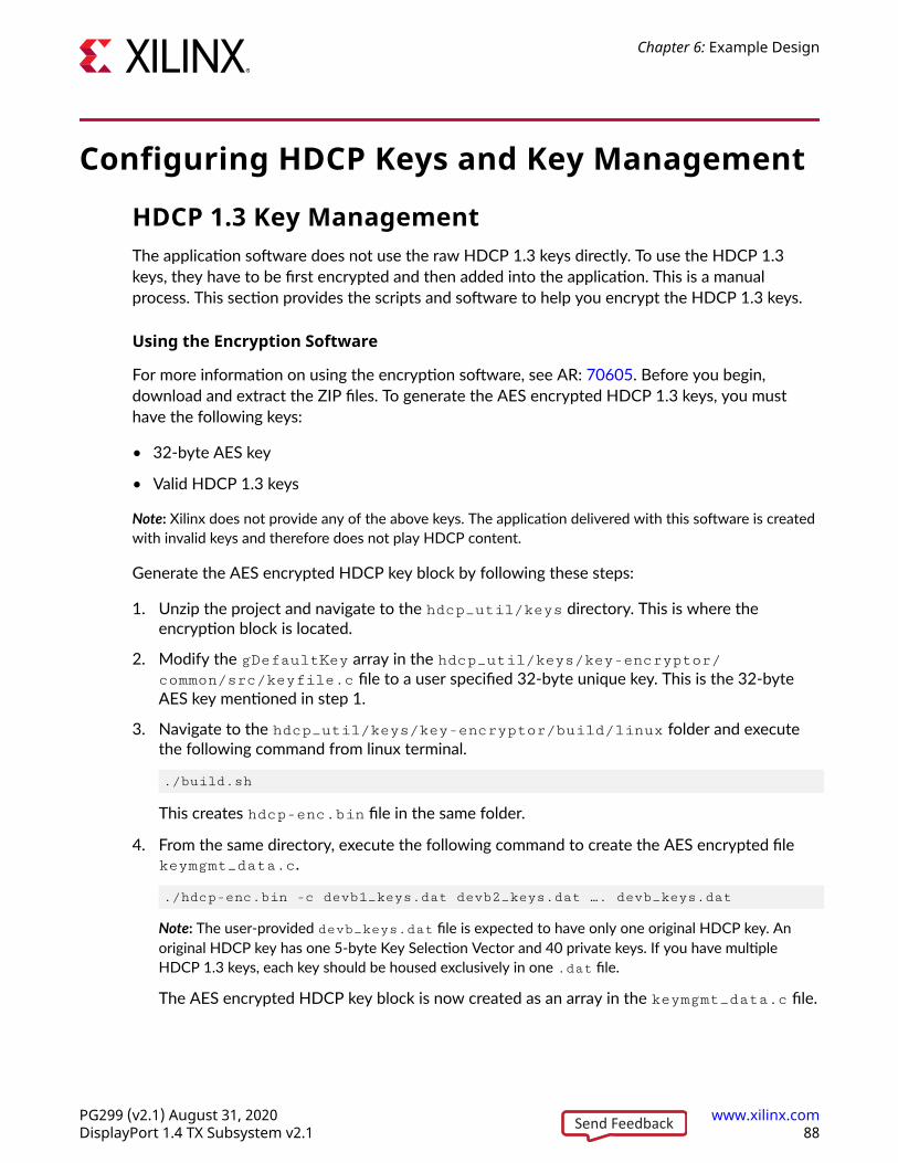
Configuring HDCP Keys and Key ManagementHDCP 1.3 Key ManagementThe application software does not use the raw HDCP 1.3 keys directly. To use the HDCP 1.3keys, they have to be first encrypted and then added into the application. This is a manualprocess. This section provides the scripts and software to help you encrypt the HDCP 1.3 keys.
Using the Encryption Software
For more information on using the encryption software, see AR: 70605. Before you begin,download and extract the ZIP files. To generate the AES encrypted HDCP 1.3 keys, you musthave the following keys:
• 32-byte AES key
• Valid HDCP 1.3 keys
Note: Xilinx does not provide any of the above keys. The application delivered with this software is createdwith invalid keys and therefore does not play HDCP content.
Generate the AES encrypted HDCP key block by following these steps:
1. Unzip the project and navigate to the hdcp_util/keys directory. This is where theencryption block is located.
2. Modify the gDefaultKey array in the hdcp_util/keys/key-encryptor/common/src/keyfile.c file to a user specified 32-byte unique key. This is the 32-byteAES key mentioned in step 1.
3. Navigate to the hdcp_util/keys/key-encryptor/build/linux folder and executethe following command from linux terminal.
./build.sh
This creates hdcp-enc.bin file in the same folder.
4. From the same directory, execute the following command to create the AES encrypted filekeymgmt_data.c.
./hdcp-enc.bin -c devb1_keys.dat devb2_keys.dat …. devb_keys.dat
Note: The user-provided devb_keys.dat file is expected to have only one original HDCP key. Anoriginal HDCP key has one 5-byte Key Selection Vector and 40 private keys. If you have multipleHDCP 1.3 keys, each key should be housed exclusively in one .dat file.
The AES encrypted HDCP key block is now created as an array in the keymgmt_data.c file.
Chapter 6: Example Design
PG299 (v2.1) August 31, 2020 www.xilinx.comDisplayPort 1.4 TX Subsystem v2.1 88Send Feedback

5. Ensure that the following AES keys in the reference design matches with the keys in step 2.
\**zcu102_system_directly**\**sw_directly**\src\keys.c
The HDCP 1.3 keys are now encrypted and ready to be used.
6. Replace the dummy 32-byte AES keys in the gDefaultKey[32] array of the exampledesign application's source file src/keymgmt_keyfile.c with the keys mentioned in step2.
7. Replace the dummy AES encrypted HDCP keys in the KEYMGMT_ENCDATA[] array of theexample design application's source file src/keys.c with the encrypted keys generated instep 5.
HDCP 2.x Key Management
1. Populate the 128 bit global constant LC128 keys in the XHdcp22Lc128[] array of thekeys.c file. Replace zeroes in the array with the LC128 keys.
2. Populate the HDCP 2.x Rx private keys in the XHdcp22RxPrivateKey[] array of thekeys.c file. Replace the zeroes in the array with Rx private keys.
3. Populate the System Renewability Revoke Check Message (SRM) keys in the Hdcp22Srm[]array of the keys.c file. Replace the zeroes in the array with the SRM keys.
Tested EquipmentThe following table lists the tested equipment used with the example design.
Table 31: Sink Equipment
Sink Type Brand Name Model NameMonitor Acer S277HKWMIDPP
Monitor Dell S2817
Monitor Dell UP3218K
Monitor Dell U3014T
Monitor Dell U2713
Monitor LG 27UD68P
Monitor LG 24UD58
Monitor Asus PQ321Q
Monitor Samsung LU28D590DS
Tester Unigraf UCD-323
Tester Unigraf UCD-400
Tester Unigraf DPR-100
Chapter 6: Example Design
PG299 (v2.1) August 31, 2020 www.xilinx.comDisplayPort 1.4 TX Subsystem v2.1 89Send Feedback

Appendix A
UpgradingThere is no direct upgrade path due to the new retimer. Xilinx® recommends starting with a newdesign.
Appendix A: Upgrading
PG299 (v2.1) August 31, 2020 www.xilinx.comDisplayPort 1.4 TX Subsystem v2.1 90Send Feedback

Appendix B
Questions and AnswersQ. Can both RX and TX be used on the same GT quad for DisplayPort?
A. Yes. The Video PHY Controller supports the capability of performing both RX and TX on theGT quads. However, they cannot be different protocols.
Q. Does the Video PHY Controller support different protocols for RX and TX?
A. No. The Video PHY Controller must use the same protocol if both RX and TX is being used.
Q. I am having link training issues. What are some things that can be done to improve linktraining?
A. Perform the following:
1. Verify that all relevant ARs are taken into account.
2. Increase the AUX_DEFER value in register offset 0x004.
Q. Does the Xilinx® subsystem support my resolution and frame rate?
A. DisplayPort should operate at any resolution and frame rate as long as the DisplayPort link isnot oversubscribed. Use the following equation to determine if the custom resolution can besupported:
(HTotal × VTotal × bits_per_component × frame rate) < (0.8 × link_lane × num_lanes)
Appendix B: Questions and Answers
PG299 (v2.1) August 31, 2020 www.xilinx.comDisplayPort 1.4 TX Subsystem v2.1 91Send Feedback

Appendix C
Driver DocumentationThe driver documentation can be found at the Xilinx GitHub page.
Appendix C: Driver Documentation
PG299 (v2.1) August 31, 2020 www.xilinx.comDisplayPort 1.4 TX Subsystem v2.1 92Send Feedback

Appendix D
Helper CoreThis appendix describes Audio Video (AV) pattern generator (av_pat_gen) , Video Frame CRC(video_frame_crc) and AXI4S Video Re-mapper (v_axi4s_remapper) helper cores. Helper cores areIPs that are not part of Vivado IP catalog but only available in the as part of example design. Theyare not supported outside the original example design context. Users are expected to designtheir own IPs in their designs.
Audio Video (AV) pattern generator(av_pat_gen)
av_pat_gen module acts as a test pattern generator for both video and audio and inpassthrough design this IP is connected before TX CRC module so as to enable user to pass testpatterns on to the TX CRC module and then to the DisplayPort TX. av_pat_gen also has aswitch for the user to select whether to pass received input video/audio data (from DP RX inpassthrough system) to its output directly, or to generate test pattern video/audio data on to itsoutput.
Note that this av_pat_gen is not part of the Display Port protocol requirements and is usedonly in the example design to assist users in validation. Hence, Xilinx do not provide separateproduct guide for av_pat_gen and do not provide support related to this IP.
Feature summary1. 1, 2 and 4 PPC are supported:
“Pixel per clock” (PPC) denotes the number of video pixels that av_pat_gen can send, perinput clock. Data outputted by av_pat_gen on vid_out_axi4s is such that the first pixelwill be aligned to the lower significant part of vid_out_axis_tdata. For example, in 4PPC mode:
vid_in_axis_tdata = {pixel3, pixel2, pixel1, pixel0}
For audio, av_pat_gen always outputs 32 bit audio sample per clock.
2. RGB, YCbCr 422 video formats are supported:
a. RGB:
Appendix D: Helper Core
PG299 (v2.1) August 31, 2020 www.xilinx.comDisplayPort 1.4 TX Subsystem v2.1 93Send Feedback

av_pat_gen outputs RGB video format such that “R” component is aligned to mostsignificant part of the pixel and “G” is aligned to least significant part of the pixel. This isto mimic DP specification in arrangement of RGB components. For example,
pixel0 = {R, B, G}
b. YCbCr 422:
av_pat_gen outputs YCbCr 422 video format such that “Cr/Cb” component is alignedto most significant part and “Y” is aligned to least significant part of the pixel. Forexample,
Pixel0 = {Cb/Cr, Y}
3. 6, 8, 10, 12 and 16 BPCs are supported:
Bits per component (BPC) denotes number of bits per component of each pixel. Bitscorresponding to components of the pixel are tightly packed. For example,
If pixel0 (RGB) is being outputted by DisplayPort with 6bpc, then
Pixel0[17:12] = R-component
Pixel0[11:6] = B-component
Pixel0[5:0] = G-component
4. Supported test patterns:
av_pat_gen can generate various types of video test patterns as listed in DP compliancespecification and can generate up to 8 channels of audio streams. Below are the videopatterns it supports
• Color ramp pattern
• Black and white vertical lines pattern
• Color square pattern
• Flat red pattern
• Flat green pattern
• Flat blue pattern
• Flat Yellow pattern
When test_pattern (address 0x308, [2:0]) is selected as 0, then video/audio stream inputis directly passed to the output of av_pat_gen. Otherwise, depending on the otherconfiguration written in to the above-mentioned configuration registers, video and audio testpatterns are generated and outputted by av_pat_gen IP.
Appendix D: Helper Core
PG299 (v2.1) August 31, 2020 www.xilinx.comDisplayPort 1.4 TX Subsystem v2.1 94Send Feedback
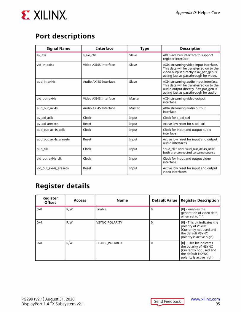
Port descriptionsSignal Name Interface Type Description
av_axi s_axi_ctrl Slave AXI Slave bus interface to supportregister interface
vid_in_axi4s Video AXI4S Interface Slave AXI4 streaming video input interface.This data will be transferred on to thevideo output directly if av_pat_gen isacting just as passthrough for video.
aud_in_axi4s Audio AXI4S Interface Slave AXI4 streaming audio input interface.This data will be transferred on to theaudio output directly if av_pat_gen isacting just as passthrough for audio.
vid_out_axi4s Video AXI4S Interface Master AXI4 streaming video outputinterface
aud_out_axi4s Audio AXI4S Interface Master AXI4 streaming audio outputinterface
av_axi_aclk Clock Input Clock for s_axi_ctrl
av_axi_aresetn Reset Input Active low reset for s_axi_ctrl
aud_out_axi4s_aclk Clock Input Clock for input and output audiointerface
aud_out_axi4s_aresetn Reset Input Active low reset for input and outputaudio interfaces
aud_clk Clock Input “aud_clk” and “aud_out_axi4s_aclk”both are connected to same source
vid_out_axi4s_clk Clock Input Clock for input and output videointerface
vid_out_axi4s_aresetn Reset Input Active low reset for input and outputvideo interfaces
Register detailsRegister
Offset Access Name Default Value Register Description
0x0 R/W Enable 0 [0] – enables thegeneration of video data,when set to ‘1’.
0x4 R/W VSYNC_POLARITY 0 [0] - This bit indicates thepolarity of VSYNC(Currently not used andthe default VSYNCpolarity is active high)
0x8 R/W HSYNC_POLARITY 0 [0] – This bit indicatesthe polarity of HSYNC(Currently not used andthe default HSYNCpolarity is active high)
Appendix D: Helper Core
PG299 (v2.1) August 31, 2020 www.xilinx.comDisplayPort 1.4 TX Subsystem v2.1 95Send Feedback

RegisterOffset Access Name Default Value Register Description
0xC R/W ENABLE_POLARITY 0 [0] – This bit indicatesthe polarity of ENABLE i.e[0] bit of 0x00 (Currentlynot used and the defaultpolarity of ENABLE isactive high).
0x10 R/W VSYNC_WIDTH 0 [13:0] – Holds the valueof VSYNC width
0x14 R/W VERT_BACK_PORCH 0 [13:0] – Holds the valueof Vertical Back Porch
0x18 R/W VERT_FRONT_PORCH 0 [13:0] – Holds the valueof Vertical Front Porch
0x1C R/W VRES 0 [13:0] - Holds the valueof Vertical ResolutionVRES
0x20 R/W HSYNC_WIDTH 0 [13:0] - Holds the valueof HSYNC width
0x24 R/W HORIZ_BACK_PORCH 0 [13:0] – Holds the valueof Horizontal Back Porch
0x28 R/W HORIZ_FRONT_PORCH 0 [13:0] – Holds the valueof Horizontal Front Porch
0x2C R/W HRES 0 [13:0] - Holds the valueof Horizontal ResolutionHRES
0x34 R/W FRAMELOCK_DELAYFRAMELOCK_ENABLE
0 [10:0] – Frame lock delay(Currently not used)[31] – Frame lock enable(Currently not used)
0x3C R/W FRAMELOCK_LINE_FRACFRAMELOCK_ALIGN_SYNC
0 [10:0] – Frame lock linefraction (Currently notused)[16] – Frame lock alignHSYNC (Currently notused)
0x40 R/W Hdcolorbar_config 0 [2:0] – HD Color barconfig (Currently notused)
0x44 R/W TC_HSBLNK 0 [13:0] – HSBLANK, holdsthe start value ofHBLANK.Number of active pixels =HSBLANK + 1For example, if HSBLANKis 4, then the number ofactive pixels before startof BLANKING region are5.
0x48 R/W TC_HSSYNC 0 [13:0] - HSSYNC, holdsthe start value of HSYNC.For example, if HSSYNCis 8, then the number oftotal pixel clocks whichoccur before HSYNC isasserted are 9.
Appendix D: Helper Core
PG299 (v2.1) August 31, 2020 www.xilinx.comDisplayPort 1.4 TX Subsystem v2.1 96Send Feedback

RegisterOffset Access Name Default Value Register Description
0x4C R/W TC_HESYNC 0 [13:0] - HESYNC, holdsthe end value of HSYNC.For example, if HESYNCis 11, then the number oftotal pixel clocks whichoccur before HSYNC isde-asserted are 10.
Note that, the totalnumber of pixel clocksfor HSYNC = HESYNC -HSSYNC
0x50 R/W TC_HEBLNK 0 [13:0] – HEBLANK, holdsthe end value ofHBLANK.For example, if HEBLANKis 20, then the number oftotal pixel clocks beforeend of BLANKING regionare 19.
Note that, the totalnumber of pixel clocksfor blanking = HEBLANK -HSBLANK
0x54 R/W TC_VSBLNK 0 [13:0] – VSBLANK, holdsthe start value ofVBLANK.Number of active lines =VSBLANK + 1For example, if VSBLANKis 4, then the number ofactive lines before startof VERTICAL BLANKINGregion are 5.
0x58 R/W TC_VSSYNC 0 [13:0] - VSSYNC, holdsthe start value of VSYNC.For example, if VSSYNC is8, then the number oftotal lines which occurbefore VSYNC is assertedare 9.
0x5C R/W TC_VESYNC 0 [13:0] - VESYNC, holdsthe end value of VSYNC.For example, if VESYNC is11, then the number oftotal lines which occurbefore VSYNC is de-asserted are 10.
Note that, the totalnumber of lines forVSYNC = VESYNC -VSSYNC
Appendix D: Helper Core
PG299 (v2.1) August 31, 2020 www.xilinx.comDisplayPort 1.4 TX Subsystem v2.1 97Send Feedback

RegisterOffset Access Name Default Value Register Description
0x60 R/W TC_VEBLNK 0 [13:0] – VEBLANK, holdsthe end value of VBLANK.For example, if VEBLANKis 20, then the number oftotal lines before end ofBLANKING region are 19.
Note that, the totalnumber of lines forblanking = HEBLANK -HSBLANK
0x300 R/W MISC0 0 [2:1] – Denotes if videoformat is RGB orYCbCr42200 – RGB01 - YCbCr 422
[3] - If asserted, thendynamic range will beenabled in RGBcolorimetry.[4] –If 0, thenYCbCr_ITU_R_BT601version of YCbCr will beenabledIf 1, thenYCbCr_ITU_R_BT709version of YCbCr will beenabled[7:5] –If 000, then 6BPCIf 001, then 8BPCIf 010, then 10BPCIf 011, then 12BPCIf 100, then 16BPC
0x304 - MISC1 0 Currently not used
Appendix D: Helper Core
PG299 (v2.1) August 31, 2020 www.xilinx.comDisplayPort 1.4 TX Subsystem v2.1 98Send Feedback

RegisterOffset Access Name Default Value Register Description
0x308 R/W Quad_pixel_modedual_pixel_modeEn_sw_patternTest_pattern
0 [2:0] – Denotes video testpattern000 – Indicates no testpattern is generated inthe IP, instead inputvideo stream is directlypassed to output.001 – Color ramp pattern010 – Blank and Whitevertical lines pattern011 – Color squarepattern100 - Flat Red pattern101 – Flat Green pattern110 – Flat Blue pattern111 – Flat yellow pattern
[4] – Currently not used[8] – When asserted, dualpixel mode is enabled[9] – When asserted,quad pixel mode isenabled
0x400 R/W Aud_resetaud_startAud_drop (Not used)
1 [0] – aud_reset, Whenasserted, the audio pathgets reset.[1] - aud_start, Whenasserted, audio testpattern data getsstarted.When de-asserted, audiopath of this IP acts as apassthrough to theincoming audio data.[2] – Currently not used.
0x404 R/W Aud_sample_rate 0 [3:0] – Holds the value ofaudio sample rate[11:8] - Holds the valueof number of audiochannels selected
0x410 R/W Aud_pattern1Aud_period1
0 [1:0] – Holds the value ofaudio pattern 100 – Indicates silence10 – Indicates ping
[11:8] – Holds the valueof audio period for audiopattern 1
0x420 R/W Aud_pattern2Aud_period2
0 [1:0] – Holds the value ofaudio pattern 2[11:8] – Holds the valueof audio period for audiopattern 2
Appendix D: Helper Core
PG299 (v2.1) August 31, 2020 www.xilinx.comDisplayPort 1.4 TX Subsystem v2.1 99Send Feedback

RegisterOffset Access Name Default Value Register Description
0x430 R/W Aud_pattern3Aud_period3
0 [1:0] – Holds the value ofaudio pattern 3[11:8] – Holds the valueof audio period for audiopattern 3
0x440 R/W Aud_pattern4Aud_period4
0 [1:0] – Holds the value ofaudio pattern 4[11:8] – Holds the valueof audio period for audiopattern 4
0x450 R/W Aud_pattern5Aud_period5
0 [1:0] – Holds the value ofaudio pattern 5[11:8] – Holds the valueof audio period for audiopattern 5
0x460 R/W Aud_pattern6Aud_period6
0 [1:0] – Holds the value ofaudio pattern 6[11:8] – Holds the valueof audio period for audiopattern 6
0x470 R/W Aud_pattern7Aud_period7
0 [1:0] – Holds the value ofaudio pattern 7[11:8] – Holds the valueof audio period for audiopattern 7
0x480 R/W Aud_pattern8Aud_period8
0 [1:0] – Holds the value ofaudio pattern 8[11:8] – Holds the valueof audio period for audiopattern 8
0x4A0 R/W Aud_channel_status 0 [31:0] – Holds the valueof channel status that isto be sent along withaudio sample
0x4A4 R/W Aud_channel_status 0 [9:0] – Holds the value ofchannel status that is tobe sent along with audiosample
0x4A8 - - - Currently not used
0x4AC - - - Currently not used
0x4B0 - - - Currently not used
0x4B4 - - - Currently not used
0x4B8 R/W Audio_chk_start 0 [0] – When asserted,internal audio checkergets started[7:4] – Holds the userdefined stream ID andthis is sent over outputTID so that otherexternal IPs know thestream ID of the audiodata being sent.
Appendix D: Helper Core
PG299 (v2.1) August 31, 2020 www.xilinx.comDisplayPort 1.4 TX Subsystem v2.1 100Send Feedback

RegisterOffset Access Name Default Value Register Description
0x4C0 R/W Audio_stream_id 0 [31:0] - Holds the countvalue after which thenumber of audio samplecounted by the internalchecker will be reset.
• Clocking: av_axi_aclk - Clock for AXI lite programming interfaceaud_out_axi4s_aclk - Clock forinput and output audio interfaceaud_clk - “aud_clk” and “aud_out_axi4s_aclk” both areconnected to same sourcevid_out_axi4s_clk - Clock for input and output video interface
• Resets:: av_axi_aresetn - Active low reset for AXI lite programminginterfaceaud_out_axi4s_aresetn - Active low reset for input and output audiointerfacesvid_out_axi4s_aresetn - Active low reset for input and output video interfaces
Programming sequence:
For Video
1. av_pat_gen work in two modes for video
Mode – 0 : When bits [2:0] value is 3’b000 in register 0x308, this IP just acts as a passthrough to the incoming video.
Mode – 1: When bits [2:0] value is not 3’b000 in register 0x308, then this IP generates testpatterns for video.
2. When mode-1 is selected, make bit [0] of 0x0 as “0” initially and configure appropriate valuesin the configuration registers (like HRES, VRES, TEST PATTERN TYPES etc.) corresponding tothe video that is intended to be generated by the test pattern generator.
3. Then program “1” to bit [0] of 0x0 to start the generation of required video test pattern.
For Audio
1. av_pat_gen work in two modes for audio
Mode – 0 : When bit [1] value is 1’b0 in register 0x400, this IP just acts as a pass through tothe incoming audio.
Mode – 1: When bit [1] value is 1’b1 in register 0x400, then this IP generates test patternsfor audio.
2. To generate audio test patterns, make bit [1] of 0x400 as “0” initially and configureappropriate values in the configuration registers (like audio_test_pattern etc.) correspondingto the audio that is intended to be generated by the test pattern generator.
3. Then program “1” to bit [1] of 0x400 to start the generation of required audio test pattern.
Appendix D: Helper Core
PG299 (v2.1) August 31, 2020 www.xilinx.comDisplayPort 1.4 TX Subsystem v2.1 101Send Feedback

4. User can enable bit [0] of 0x4B8, to start the internal audio checker of the IP which performscounting of number of audio samples being outputted by the IP. However currently there isno support to read this count through register interface. This checker can be used to countthe audio samples on the input data when bit [1] of register 0x400 is programmed as 0.
Video Frame CRC (video_frame_crc)Cyclic Redundancy Check (CRC) is generally used to detect errors in digital data and is commonlyemployed in video transmission to detect errors in pixel transmission. Using CRC, data integritycan be checked at various levels namely, pixel level, horizontal line level, frame level of a video.
CRC (video_frame_crc) is used in Display Port’s example designs to calculate CRC at frame level,on the data received by Display Port RX subsystem and on the data being fed to Display Port TXsubsystem (in passthrough system). Each color component’s CRC value is calculated separatelyonce per every frame and can be compared with the transmitted video frame’s CRC value tocheck the data integrity.
Note that, CRC is not part of the Display Port core data path requirements but is necessary forvalidation/compliance requirements as per DP 1.4a specification. Xilinx’s CRC IP complies to therequirements mentioned in DP 1.4a specification but do not provide separate product guide forCRC and do not provide support related to this CRC IP.
Feature summary• 1,2 and 4 PPCs are supported:
Data is received by video_frame_crc on Vid_In_AXIS such that the first pixel will bealigned to the lower significant part of vid_in_axis_tdata. For example, in 4 PPC mode,
vid_in_axis_tdata = {pixel3, pixel2, pixel1, pixel0}
• RGB, YCbCr 422 video formats are supported:
○ RGB:
DisplayPort outputs YCbCr 422 video format such that Cr/Cb component is aligned tomost significant part and “Y” is aligned to least significant part of the pixel. For example,
If pixel0 (YCbCr) is being outputted by DisplayPort to video_frame_crc, then
Pixel0 = {Cb/Cr, Y}
○ YCbCr 422:
DisplayPort outputs YCbCr 422 video format such that Cr/Cb component is aligned tomost significant part and “Y” is aligned to least significant part of the pixel. For example,
If pixel0 (YCbCr) is being outputted by DisplayPort to video_frame_crc, then
Appendix D: Helper Core
PG299 (v2.1) August 31, 2020 www.xilinx.comDisplayPort 1.4 TX Subsystem v2.1 102Send Feedback

Pixel0 = {Cb/Cr, Y}
• 6, 8, 10, 12 and 16 BPCs are supported:
Bits corresponding to components of the pixel are tightly packed. For example,
If pixel0 (RGB) is being outputted by DisplayPort with 6bpc, then
Pixel0[17:12] = R-component
Pixel0[11:6] = B-component
Pixel0[5:0] = G-component
Port descriptionsSignal name Interface Type Description
S_AXI s_axi_ctrl Slave AXI Slave bus interface tosupport register interface
Vid_In_AXIS Video AXI4S Interface Slave AXI4 streaming video inputinterface to receive data onwhich CRC is to becalculated.
Vid_Out_AXIS Video AXI4S Interface Master AXI4 streaming video outputinterface for passing theinput data to next IPs in thevideo pipeline
s_axi_aclk Clock Input Clock for s_axi_CTRL
s_axi_aresetn Reset Input Active low reset fors_axi_CTRL
vid_in_axis_aclk Clock Input Clock for input and outputstreaming video interfaces
vid_in_axis_aresetn Reset Input Active low reset for input andoutput streaming videointerfaces
Register detailsRegister
offset Access Name Default Value Register description
0x0 R/W Pixel Mode 0x1 [2:0] -3’b001 – 1PPC,3’b010 – 2PPC,3’b100 – 4PPC[4] - When set to ‘1’, this clearsall the CRC values[31] - When set to ‘1’, thisspecifies that the incoming datais YCbCr 422 mode.
Appendix D: Helper Core
PG299 (v2.1) August 31, 2020 www.xilinx.comDisplayPort 1.4 TX Subsystem v2.1 103Send Feedback

Registeroffset Access Name Default Value Register description
0x4 R G_CRCR_CRC
0 [15:0] - CRC value of ‘R’component in RGB mode and‘Cr’ component in YCbCr 422mode[31:16] - CRC value of ‘G’component in RGB mode and‘Cb’ component in YCbCr 422mode
0x8 R B_CRC 0 [15:0] - CRC value of ‘B’component in RGB mode and ‘Y’component in YCbCr 422 mode
0xC R/W HACTIVEVACTIVE
0 [15:0] - Denotes number ofHACTIVE pixels[31:16] – Denotes number ofVACTIVE Lines
0x10 R Red_missGreen_missBlue_miss
0 [3:0] – Denotes number ofmissing ‘R’ components in RGBmode andnumber of missing ‘Cr’components in YCbCr 422 mode[7:4] – Denotes number ofmissing ‘G’ components in RGBmode andnumber of missing ‘Cb’components in YCbCr 422 mode[11:8] – Denotes number ofmissing ‘B’ components in RGBmode andnumber of missing ‘Y’components in YCbCr 422 mode
• Clocking:: s_axi_aclk - Clock for s_axi_ctrl register interfacevid_in_axis_aclk -Clock for input and output streaming video interface
• Resets:: s_axi_aresetn - This reset when enabled, resets all the registers to defaultvaluesvid_in_axis_aresetn - This reset when enabled, reset the entire data path relatedto CRC calculations.
• Programming sequence:: Program HACTIVE, VACTIVE, PPC and color formats in to theregisters before inputting corresponding video stream data.On every VSYNC of the frame, 0x4and 0x8 registers are updated with the calculated CRC values. Hence the values in 0x4 and0x8 registers denote CRC values calculated for the previous frame.
FunctionalityCRC is calculated per component for the entire frame and the final CRC value per component iswritten in to the register for the software to read (in addresses 0x4 and 0x8), once VSYNC isdetected. Hence, if the input is 1PPC RGB, then total of 3 CRC modules are needed for eachcomponent. Similarly, if it is 2 PPC, then total of 6 CRC modules are needed.
Appendix D: Helper Core
PG299 (v2.1) August 31, 2020 www.xilinx.comDisplayPort 1.4 TX Subsystem v2.1 104Send Feedback

Polynomial used is,
f(x) = x16 + x15 + x2 + 1
Implementation is done as mentioned in the appendix of DP 1.4a specification except for the factthat there is an extra “init” input which takes the result of the CRC module from the previousclock cycle. In DP 1.4a specification, there is no separate input for previous clock’s CRC output.Instead it is denoted directly with the name of the output (which is ‘d’) of CRC module. The valueof the per component’s CRC module’s output (‘dout’ in the example below) when VSYNC isdetected is considered as the final calculated CRC value of specific component in that frame.
• Special case for YCbCr 422 mode in 1PPC mode:: For RGB video format, calculation of CRCper component is straight forward, but for YCbCr 422 mode, VESA recommends calculatingCRC for each of the component namely Y, Cb and Cr. Hence there will be a special case ofhandling the data when it is 1PPC mode. This is because on Vid_In_AXIS_tdata, Cb and Cralternate on the same most significant part of the data on every clock cycle in 1PPC mode andcare is taken such that the same part of the data is routed to CRC module handling ‘Cb’ on oneclock and to the CRC module handling ‘Cr’ on another clock. In this mode, for each of the ‘Cb’and ‘Cr’ components, same data (din and init) will be held for 2 clock cycles at their respectiveCRC module’s inputs since there will be only one “Cb” component and only one “Cr”component per 2 clock cycles in 1 PPC mode.
• Examples::
• Block diagram of per component CRC calculator in 1PPC mode: Here, “din” is loaded onevery clock cycle, with data corresponding to a component of each pixel.
Figure 25: CRC calculator in 1PPC mode
CRC
Delay
din
init
dout
X23218-091619
Appendix D: Helper Core
PG299 (v2.1) August 31, 2020 www.xilinx.comDisplayPort 1.4 TX Subsystem v2.1 105Send Feedback

• Block diagram of per component CRC calculator in 2PPC mode: Here, “din1” and “din2”are loaded on every clock cycle, with data corresponding to a component of twoconsecutive pixels received in same clock (since 2 PPC mode).
Figure 26: CRC calculator in 2PPC mode
CRC(Pixel 0)
CRC(Pixel 1)
Delay
doutinit2init1 dout tempdin1 din2
X23219-091619
AXI4S Video Re-mapper (v_axi4s_remapper)v_axi4s_remapper is used in DisplayPort example designs to remap video pixels betweendifferent “pixel per clock (PPC)” requirements. Multiple color formats are supported for remapnamely, YUV444, YUV422 and YUV420. This IP is employed in DP TX data pipeline after framebuffer and in DP RX data pipeline before frame buffer in DP example designs, as the frame bufferalways outputs data in 4PPC mode, but we may require other PPC modes for DP TX and RX.
Apart from “PPC” conversion, this IP also supports pixel drop and pixel repeat features whichenables dropping and repetition of user specific pixels on the output and supportsYUV420_HDMI color format too, which are out of scope of this document.
Note that this v_axi4s_remapper is not part of the Display Port protocol requirements and isused only in the example design to assist users in validation. Hence, Xilinx do not provideseparate product guide for v_axi4s_remapper and do not provide support related to this IP.
Feature summary
1. 1,2 and 4 PPC support
v_axi4s_remap supports mapping of AXI4S stream video data between 1,2 and 4 PPCmodes. For enabling the feature of PPC conversions, “Convert Samples per clock” needs to beselected in the GUI of the IP.
Appendix D: Helper Core
PG299 (v2.1) August 31, 2020 www.xilinx.comDisplayPort 1.4 TX Subsystem v2.1 106Send Feedback
This IP has two register configurable values namely, “inPixClk” and “outPixClk” (as mentionedin Register details section), which specifies the PPC on input and the PPC required on outputrespectively. These values are used by the IP for remapping between various PPCs.
In all the PPCs, first pixel is aligned to the lower significant part of video AXI4S stream’sTDATA. For example, in 4PPC mode
vid_in_axis_tdata / vid_out_axis_tdata = {pixel3, pixel2, pixel1, pixel0}
2. YUV444/RGB, YUV422, YUV420 video formats support
v_axi4s_remap does not manipulate the component order in each pixel as it only alters thenumber of pixels per clock. Hence, the DisplayPort specific input component ordering onv_axi4s_remap is preserved on the output of the IP.
Also, BPCs does not matter for re-mapper module as it only manipulates video data bits interms of pixels. Hence, all the BPCs are supported by this IP.
Port descriptionSignal name Interface Type Description
s_axi_CTRL s_axi_ctrl Slave AXI Slave bus interface tosupport register interface
s_axis_video Video AXI4S Interface Slave AXI4 streaming video inputinterface.
m_axis_video Video AXI4S Interface Master AXI4 streaming video outputinterface.
ap_clk Clock Input Clock for streaming interfaceand s_axi_CTRL
ap_reset_n Reset Input Active low reset forstreaming interface ands_axi_CTRL
Register detailsRegister Offset Access Name Default Value Register Description0x10 R/W Picture Height 0 [15:0] Holds the value of picture
height
0x18 R/W Picture Width 0 [15:0] Holds the value of picturewidth
0x20 R/W Picture Color format 1 [7:0] Holds the value of colorformat8’h1 – For YUV4448’h3 – For YUV422 / YUV420
0x28 R/W inPixClk 0 [7:0] – Holds the value ofnumber of pixels per clock onthe input video streaminginterface
Appendix D: Helper Core
PG299 (v2.1) August 31, 2020 www.xilinx.comDisplayPort 1.4 TX Subsystem v2.1 107Send Feedback

Register Offset Access Name Default Value Register Description0x30 R/W outPixClk 0 [7:0] – Holds the value of
number of pixels per clockrequired on the output videostreaming interface
0x38 - - This is out of scope as it ismeant for HDMI
0x40 - - This is out of scope as it ismeant for HDMI
0x48 R/W inPixDrop 0 [0] – When asserted, pixel dropfeature on the input videostream gets enabled. Thisfeature is not used inDisplayPort.
0x50 R/W outPixRepeat 0 [0] – When asserted, pixelrepeat feature on the outputvideo stream gets enabled. Thisfeature is not used inDisplaypPort.
• Clocking:: This IP has only one clock namely ap_clk on which all of the three interfaces(s_axi_ctrl, s_axis_video and m_axis_video) work.
• Resets:: This IP has an active low reset namely, ap_reset_n which when enabled, puts allthe registers in default state.
• Programming sequence::
• The IP should be generated with “Convert Samples per clock” feature enabled in GUI so asto support re-mapping between various PPCs.
• Always program the pic height, width, color format, inPixClk and outPixClk values beforeinputting the corresponding video streaming data.
• Functionality::
• AXIvideo2MultiPixStream: In this first stage of data path, the input AXI video stream datais converted in to multi pixel data basing on the inPixClk value which tells how manypixels are being inputted per input clock.
• pixClkUpConvert, pixClkDownConvert: The output from the first stage comes to thisstage, where appropriate up conversion followed by down conversion takes place tooutput required PPC.
• MultiPixStream2AXIvideo: In this final stage, the up and down converted multi pixelstream is again converted to AXI video stream output which is finally mapped to outputm_axis_video interface.
Appendix D: Helper Core
PG299 (v2.1) August 31, 2020 www.xilinx.comDisplayPort 1.4 TX Subsystem v2.1 108Send Feedback

Appendix E
DebuggingThis appendix includes details about resources available on the Xilinx® Support website anddebugging tools.
If the IP requires a license key, the key must be verified. The Vivado® design tools have severallicense checkpoints for gating licensed IP through the flow. If the license check succeeds, the IPcan continue generation. Otherwise, generation halts with an error. License checkpoints areenforced by the following tools:
• Vivado Synthesis
• Vivado Implementation
• write_bitstream (Tcl command)
IMPORTANT! IP license level is ignored at checkpoints. The test confirms a valid license exists. It does notcheck IP license level.
Finding Help on Xilinx.comTo help in the design and debug process when using the subsystem, the Xilinx Support web pagecontains key resources such as product documentation, release notes, answer records,information about known issues, and links for obtaining further product support. The XilinxCommunity Forums are also available where members can learn, participate, share, and askquestions about Xilinx solutions.
DocumentationThis product guide is the main document associated with the subsystem. This guide, along withdocumentation related to all products that aid in the design process, can be found on the XilinxSupport web page or by using the Xilinx® Documentation Navigator. Download the XilinxDocumentation Navigator from the Downloads page. For more information about this tool andthe features available, open the online help after installation.
Appendix E: Debugging
PG299 (v2.1) August 31, 2020 www.xilinx.comDisplayPort 1.4 TX Subsystem v2.1 109Send Feedback

Answer RecordsAnswer Records include information about commonly encountered problems, helpful informationon how to resolve these problems, and any known issues with a Xilinx product. Answer Recordsare created and maintained daily ensuring that users have access to the most accurateinformation available.
Answer Records for this subsystem can be located by using the Search Support box on the main Xilinx support web page. To maximize your search results, use keywords such as:
• Product name
• Tool message(s)
• Summary of the issue encountered
A filter search is available after results are returned to further target the results.
Master Answer Record for the DisplayPort 1.4 TX Subsystem
AR 70295
Technical SupportXilinx provides technical support on the Xilinx Community Forums for this LogiCORE™ IP productwhen used as described in the product documentation. Xilinx cannot guarantee timing,functionality, or support if you do any of the following:
• Implement the solution in devices that are not defined in the documentation.
• Customize the solution beyond that allowed in the product documentation.
• Change any section of the design labeled DO NOT MODIFY.
To ask questions, navigate to the Xilinx Community Forums.
Debug ToolsThere are many tools available to address TX design issues. It is important to know which toolsare useful for debugging various situations.
Appendix E: Debugging
PG299 (v2.1) August 31, 2020 www.xilinx.comDisplayPort 1.4 TX Subsystem v2.1 110Send Feedback
Vivado Design Suite Debug FeatureThe Vivado® Design Suite debug feature inserts logic analyzer and virtual I/O cores directly intoyour design. The debug feature also allows you to set trigger conditions to capture applicationand integrated block port signals in hardware. Captured signals can then be analyzed. Thisfeature in the Vivado IDE is used for logic debugging and validation of a design running in Xilinx®
devices.
The Vivado logic analyzer is used to interact with the logic debug LogiCORE IP cores, including:
• ILA 2.0 (and later versions)
• VIO 2.0 (and later versions)
See the Vivado Design Suite User Guide: Programming and Debugging (UG908).
Hardware DebugHardware issues can range from link bring-up to problems seen after hours of testing. Thissection provides debug steps for common issues. Xilinx® recommends having an externalauxiliary channel analyzer to understand the transactions between the Source and Sink cores.
TX General Checks• Check the DisplayPort Source is DisplayPort 1.4 compliant.
• Ensure you are using proper DisplayPort 1.4 certified cable which is tested to run at 8.1 Gb/s.
• Ensure that the Signal Integrity of the lines is as per the DisplayPort standards for the AUX,TX, and Clock Input lines.
Transmit – Training IssueThis section contains debugging steps for issues with the clock recovery or channel equalizationat sink and if the Training Done is Low.
1. Try with a working sink such as the DisplayPort Analyzer sink device.
2. Use a DisplayPort 1.4 certified cable. Change the cable and check again.
3. Put a DisplayPort AUX Analyzer in the Transmit path and check if the various training stagesmatch with those mentioned in Main Link Setup and Management.
4. Probe the lnk_clk output and check if the SI of the clock is within the Phase Noise mask ofthe respective GT.
Appendix E: Debugging
PG299 (v2.1) August 31, 2020 www.xilinx.comDisplayPort 1.4 TX Subsystem v2.1 111Send Feedback

5. Check status registers in the Video PHY Controller for Reset done (0x0020) and PLL lockStatus (0x0018).
Related InformationMain Link Setup and Management
Transmit – Main Link Problem After TrainingThis section contains debugging steps if the monitor is not displaying video even after asuccessful training or if the monitor display is noisy and has many errors.
1. Perform a software reset on the register (0x01C) and check if the video is correct now.
2. Check if the MAIN_STREAM_ENABLE register is set to 1.
3. Ensure that the MSA parameters match the Video being sent by TX.
4. Check the video pixel clock generation. Ensure that the Video Clock is based on theresolution being sent.
5. Dump the DisplayPort source registers and compare against a working log.
6. Check the symbol and disparity errors in the Sink through the DPCD registers. This could bedue to cable issue or PHY (GT) alignment issue.
Transmit – AudioThis section contains debugging steps for issues with audio communication.
1. Check if MAUD and NAUD registers are correctly programmed and aud_clk is calculated asexpected to be 512 × fs.
2. Follow steps mentioned in Programming DisplayPort Source.
3. Check if the TX_AUDIO_CHANNELS register value matches with the input audio samplessent.
4. Check if the TX_AUDIO_INFO_DATA is correctly formatted as per CEA 861-C info framespecification.
5. Ensure all the inputs data bits of s_axis_audio_ingress_tdata ands_axis_audio_ingress_tid are correctly sent as per the format specified.
Related InformationProgramming DisplayPort Source
Transmit – Misaligned DataThis section contains debugging steps for issues with data appearing to be misaligned or shiftedon the monitor.
Appendix E: Debugging
PG299 (v2.1) August 31, 2020 www.xilinx.comDisplayPort 1.4 TX Subsystem v2.1 112Send Feedback

1. Check the EDID timings to verify they are within the CVT standard RB and RB2 reducedblanking resolutions.
2. Using EDID timings outside of the CVT standard can cause timing issues.
To fix this, define VTC_ADJUST_FOR_BS_TIMING in the xdptxss_vtc.c. This moves the BSsymbol into the front porch to fix a swing in the BS timing caused by a non-standard CVT timing.
Software DebugThis section shows how to navigate to the DisplayPort debug driver information.
1. Open the platform project file, select Board Support Package under standalone and click onModify BSP settings.
2. Add the option -DDEBUG to the extra compiler flags then close the BSP settings.
Appendix E: Debugging
PG299 (v2.1) August 31, 2020 www.xilinx.comDisplayPort 1.4 TX Subsystem v2.1 113Send Feedback

3. Select the platform and click build.
This will enable the debug symbol.
Appendix E: Debugging
PG299 (v2.1) August 31, 2020 www.xilinx.comDisplayPort 1.4 TX Subsystem v2.1 114Send Feedback

Appendix F
Additional Resources and LegalNotices
Xilinx ResourcesFor support resources such as Answers, Documentation, Downloads, and Forums, see XilinxSupport.
Documentation Navigator and Design HubsXilinx® Documentation Navigator (DocNav) provides access to Xilinx documents, videos, andsupport resources, which you can filter and search to find information. To open DocNav:
• From the Vivado® IDE, select Help → Documentation and Tutorials.
• On Windows, select Start → All Programs → Xilinx Design Tools → DocNav.
• At the Linux command prompt, enter docnav.
Xilinx Design Hubs provide links to documentation organized by design tasks and other topics,which you can use to learn key concepts and address frequently asked questions. To access theDesign Hubs:
• In DocNav, click the Design Hubs View tab.
• On the Xilinx website, see the Design Hubs page.
Note: For more information on DocNav, see the Documentation Navigator page on the Xilinx website.
ReferencesThese documents provide supplemental material useful with this guide:
Appendix F: Additional Resources and Legal Notices
PG299 (v2.1) August 31, 2020 www.xilinx.comDisplayPort 1.4 TX Subsystem v2.1 115Send Feedback

1. Video PHY Controller LogiCORE IP Product Guide (PG230)
2. UltraFast Design Methodology Guide for the Vivado Design Suite (UG949)
3. VESA DisplayPort Standard (VESA website)
4. Vivado Design Suite User Guide: Designing IP Subsystems using IP Integrator (UG994)
5. AXI4-Stream Video IP and System Design Guide (UG934)
6. SmartConnect LogiCORE IP Product Guide (PG247)
7. Vivado Design Suite User Guide: Designing with IP (UG896)
8. Vivado Design Suite User Guide: Getting Started (UG910)
9. Vivado Design Suite User Guide: Logic Simulation (UG900)
10. Vivado Design Suite User Guide: Programming and Debugging (UG908)
11. Vivado Design Suite User Guide: Implementation (UG904)
12. Vivado Design Suite: AXI Reference Guide (UG1037)
13. AXI4-Stream to Video Out LogiCORE IP Product Guide (PG044)
14. Video Timing Controller LogiCORE IP Product Guide (PG016)
15. HDCP 1.x Product Guide (PG224)
16. AXI Timer LogiCORE IP Product Guide (PG079)
17. ZCU102 System Controller GUI Tutorial (registration required) (XTP433)
18. VCU118 System Controller Tutorial (registration required) (XTP447)
19. UltraScale Architecture and Product Data Sheet: Overview (DS890)
20. Kintex UltraScale FPGAs Data Sheet: DC and AC Switching Characteristics (DS892)
21. Virtex UltraScale FPGAs Data Sheet: DC and AC Switching Characteristics (DS893)
22. Defense-Grade UltraScale Architecture Data Sheet: Overview (DS895)
23. Kintex UltraScale+ FPGAs Data Sheet: DC and AC Switching Characteristics (DS922)
24. Virtex UltraScale+ FPGA Data Sheet: DC and AC Switching Characteristics (DS923)
25. Zynq UltraScale+ MPSoC Data Sheet: DC and AC Switching Characteristics (DS925)
26. Zynq UltraScale+ RFSoC Data Sheet: DC and AC Switching Characteristics (DS926)
Revision HistoryThe following table shows the revision history for this document.
Appendix F: Additional Resources and Legal Notices
PG299 (v2.1) August 31, 2020 www.xilinx.comDisplayPort 1.4 TX Subsystem v2.1 116Send Feedback

Section Revision Summary08/31/2020 v2.1
Chapter 2: Overview Updated with device specific line rate information.
Chapter 4: Designing with the Subsystem Added eDP support.
Chapter 6: Example Design Added Configuring HDCP Keys and Key Managementsections.
12/02/2019 v2.1
General updates • HDCP 2.2 support• FB Pass-through with HDCP 1.3 and HDCP 2.2• Added Appendix D for helper cores• Vitis flow updated in chapter 6
05/22/2019 v2.1
Chapter 6: Example Design MST FB Pass-through example design details added
12/05/2018 v2.0
MST Interface Added MST interface ports
HDCP Key Interface HDCP Ports added
Programming the Core in MST Mode MST Programming added
Pixel Mapping Examples on AXI4-Stream Interface (UG934-Compliant)
UG934-compliant pixel mapping
04/04/2018 v1.0
Initial release. N/A
Please Read: Important Legal NoticesThe information disclosed to you hereunder (the "Materials") is provided solely for the selectionand use of Xilinx products. To the maximum extent permitted by applicable law: (1) Materials aremade available "AS IS" and with all faults, Xilinx hereby DISCLAIMS ALL WARRANTIES ANDCONDITIONS, EXPRESS, IMPLIED, OR STATUTORY, INCLUDING BUT NOT LIMITED TOWARRANTIES OF MERCHANTABILITY, NON-INFRINGEMENT, OR FITNESS FOR ANYPARTICULAR PURPOSE; and (2) Xilinx shall not be liable (whether in contract or tort, includingnegligence, or under any other theory of liability) for any loss or damage of any kind or naturerelated to, arising under, or in connection with, the Materials (including your use of theMaterials), including for any direct, indirect, special, incidental, or consequential loss or damage(including loss of data, profits, goodwill, or any type of loss or damage suffered as a result of anyaction brought by a third party) even if such damage or loss was reasonably foreseeable or Xilinxhad been advised of the possibility of the same. Xilinx assumes no obligation to correct anyerrors contained in the Materials or to notify you of updates to the Materials or to productspecifications. You may not reproduce, modify, distribute, or publicly display the Materialswithout prior written consent. Certain products are subject to the terms and conditions ofXilinx's limited warranty, please refer to Xilinx's Terms of Sale which can be viewed at https://
Appendix F: Additional Resources and Legal Notices
PG299 (v2.1) August 31, 2020 www.xilinx.comDisplayPort 1.4 TX Subsystem v2.1 117Send Feedback

www.xilinx.com/legal.htm#tos; IP cores may be subject to warranty and support terms containedin a license issued to you by Xilinx. Xilinx products are not designed or intended to be fail-safe orfor use in any application requiring fail-safe performance; you assume sole risk and liability foruse of Xilinx products in such critical applications, please refer to Xilinx's Terms of Sale which canbe viewed at https://www.xilinx.com/legal.htm#tos.
AUTOMOTIVE APPLICATIONS DISCLAIMER
AUTOMOTIVE PRODUCTS (IDENTIFIED AS "XA" IN THE PART NUMBER) ARE NOTWARRANTED FOR USE IN THE DEPLOYMENT OF AIRBAGS OR FOR USE IN APPLICATIONSTHAT AFFECT CONTROL OF A VEHICLE ("SAFETY APPLICATION") UNLESS THERE IS ASAFETY CONCEPT OR REDUNDANCY FEATURE CONSISTENT WITH THE ISO 26262AUTOMOTIVE SAFETY STANDARD ("SAFETY DESIGN"). CUSTOMER SHALL, PRIOR TO USINGOR DISTRIBUTING ANY SYSTEMS THAT INCORPORATE PRODUCTS, THOROUGHLY TESTSUCH SYSTEMS FOR SAFETY PURPOSES. USE OF PRODUCTS IN A SAFETY APPLICATIONWITHOUT A SAFETY DESIGN IS FULLY AT THE RISK OF CUSTOMER, SUBJECT ONLY TOAPPLICABLE LAWS AND REGULATIONS GOVERNING LIMITATIONS ON PRODUCTLIABILITY.
Copyright
© Copyright 2018-2020 Xilinx, Inc. Xilinx, the Xilinx logo, Alveo, Artix, Kintex, Spartan, Versal,Virtex, Vivado, Zynq, and other designated brands included herein are trademarks of Xilinx in theUnited States and other countries. AMBA, AMBA Designer, Arm, ARM1176JZ-S, CoreSight,Cortex, PrimeCell, Mali, and MPCore are trademarks of Arm Limited in the EU and othercountries. The DisplayPort Icon is a trademark of the Video Electronics Standards Association,registered in the U.S. and other countries. All other trademarks are the property of theirrespective owners.
Appendix F: Additional Resources and Legal Notices
PG299 (v2.1) August 31, 2020 www.xilinx.comDisplayPort 1.4 TX Subsystem v2.1 118Send Feedback


