28
Slide 1 MC Escher Immersion EUV Double Patterning DPT Challenges & Litho Solutions Bob Socha ASML
| Date post: | 28-May-2019 |
| Category: |
Documents |
| Upload: | doankhuong |
| View: | 212 times |
| Download: | 0 times |

Slide 1
MC
Esc
her
Immersion
EUV
Double
Patter
ning
DPT Challenges & Litho Solutions
Bob SochaASML
/ Slide 2
Outline
SRAM gate DPT example
− Overlay, CDU, Resolution (Design) trade-off
Spacer Challenges
Litho Improvements to Enable LELE & LFLE DPT
Conclusion

/ Slide 3
Outline
SRAM gate DPT example
− Overlay, CDU, Resolution (Design) trade-off
Spacer Challenges
Litho Improvements to Enable LELE & LFLE DPT
Conclusion

/ Slide 4
Typical SRAM Gate Layer
Unit Cell needed for Area Calculation
• The Area of the SRAM cell is the most widely used Metric to determine the shrink of the node• As a result, the area must also be used to compare Litho-DPT to Spacer-DPT shrink capabilities.
•Comparison between Litho-DPT to Spacer-DPT based on 1-D geometries (1Dmetric) is not relevant
Pitch < 0.5λ/NA
w+CDUSE
s+OVSE
L+CDUSE
B+OVSE
ASE is a function of 3 variables RSE, OVSE and CDSE

/ Slide 5
Process Steps Required
LELE Spacer

/ Slide 6
Double patterning require better and more lithography
Litho exposure equipment parameter as percentage of CD
Single exposure
Litho double patterning
Spacer double
patterning
∆CD 7% 3.5% 3%
7-20%*
#mask steps 1 2 2-3
# process steps relative to single exposure 1 2 3-4
Application 2D, All 2D, All 1D, Mainly Memory
Overlay (depending on DFM) 20% 7%
* Depending on the amount of “Design For Manufacturing” effort

/ Slide 7
OVSE and CDUSE requirements for 35nm HP SRAM(shrink of the 50nm HP SE SRAM area by 50%)
k1 Litho-DPT• Below 50% line is the area of interest• OVSE must be less than 2.5nm for 50% shrink with Litho-DPT at CDUSE=3nm• If current CDUSE=3nm and OVSE=5nm, a 56.2% shrink can be done with Litho-DPT• If current CDUSE=3nm and OVSE=5nm, a 49.5% shrink can be done with Spacer-DPT
k1 Spacer-DPT
/ Slide 8
Outline
SRAM gate DPT example
− Overlay, CDU, Resolution (Design) trade-off
Spacer Challenges
Litho Improvements to Enable Litho-Etch-Litho-Etch DPT
Conclusion

/ Slide 9
Litho cost per layer: estimates for 32 nm & 22 nm Single exposure schemes more cost effective
45nm 32nm 32nm 32nm 22nm 22nm 22nm 22nmArFi Spacer LELE LFLE Spacer LELE LFLE EUV
Process
Nor
mal
ized
cos
t per
laye
r
Fixed Variable Source Chemical CVD Metrology Etch Freeze Ash Clean CMP

/ Slide 10
Spacer process can be used for random structuresDesired layout After spacer process applied

/ Slide 11
Spacer needs overlay friendly layout to enjoy overlay advantage from the self aligned process
Areas surrounded by geometry formed by spacer are less sensitive to overlay errors.Areas not surrounded by geometry formed by spacer are more sensitive to overlay errors. Possible CD error or bridging can occur.Without design change, overlay is still critical for spacer when exposing a clear field mask!

/ Slide 12
Spacer with overlay friendly layout to enjoy overlay advantage from the self aligned process
In areas not surrounded by geometry formed by spacer, the space width between patterns must increase.Design change to increase the space width between patterns may need tighter overlay for next layer.Design change to shift a pattern to increase space width may require verification of the electrical performance.With these design changes, the cell size may increase.

/ Slide 13
Spacer Challenges
CoO is higher with Spacer DPT compared to LELE/LFLE DPT− Spacer process integration/complexity increases cycle time
Not all designs can benefit from Spacer DPT self-alignment− Burdens the designer or makes design rules overly restrictive− Industry not yet ready for Spacer friendly designs
How can litho improvements mitigate the Spacer Challenges?

/ Slide 14
Outline
SRAM gate DPT example
− Overlay, CDU, Resolution (Design) trade-off
Spacer Challenges
Litho Improvements to Enable LELE & LFLE DPT
Conclusion

/ Slide 15Slide 15 |
Improved overlay performance options:
DCO ≤ 3.5 nmSMO ≤ 4.0 nmMMO ≤ 7.0 nm
iClean option boosts systemcleanliness and reliability
Best-in-class immersion productivity (PEP & TOP options):
148 wph (300 mm) 125 x 16x32 x 30 mJ/cm2
Faster chuck swapFaster measure cycle
Advanced lens control means improved imaging performance @ 38 nm resolution
TWINSCAN™ XT:1950Hi
Liquid particle counter option gives fast feedback and control of immersion water quality
Slide 15 |
/ Slide 16
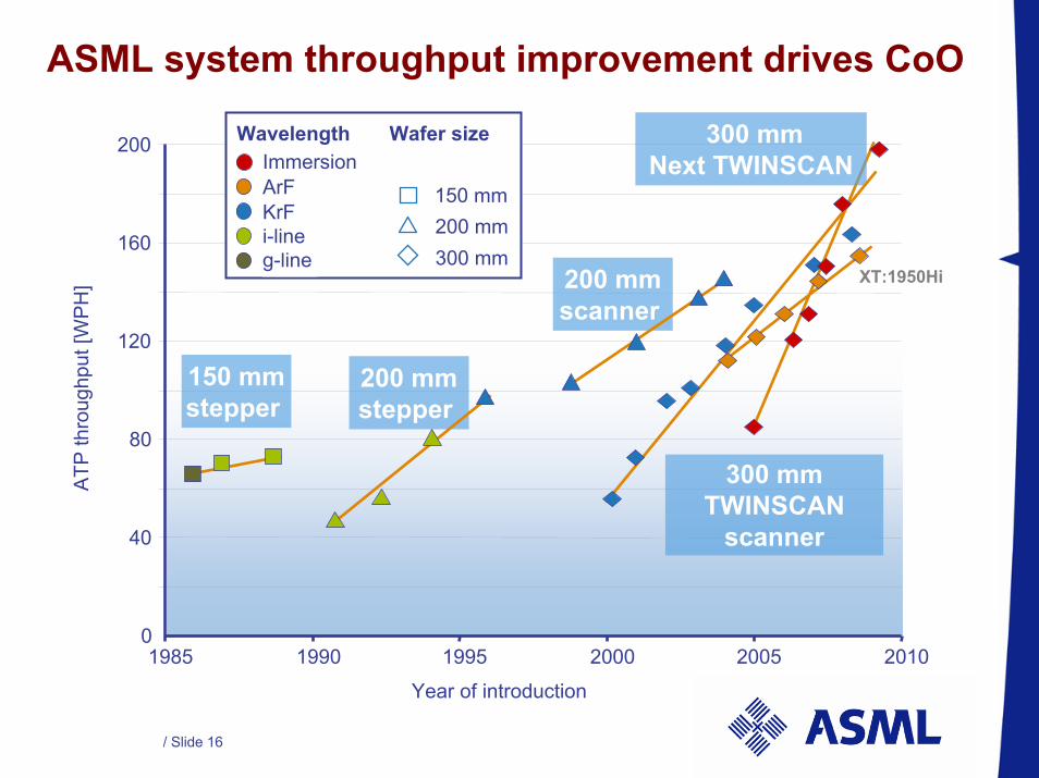
ASML system throughput improvement drives CoO
0
40
80
120
160
200
1985 1990 1995 2000 2005 2010
g-line i-line KrF ArF Immersion
Wavelength Wafer size
200 mm stepper
150 mmstepper
200 mm scanner
300 mmTWINSCAN
scanner
XT:1950Hi
300 mmNext TWINSCAN
150 mm 200 mm 300 mm
ATP
thro
ughp
ut [W
PH
]
Year of introduction
/ Slide 17
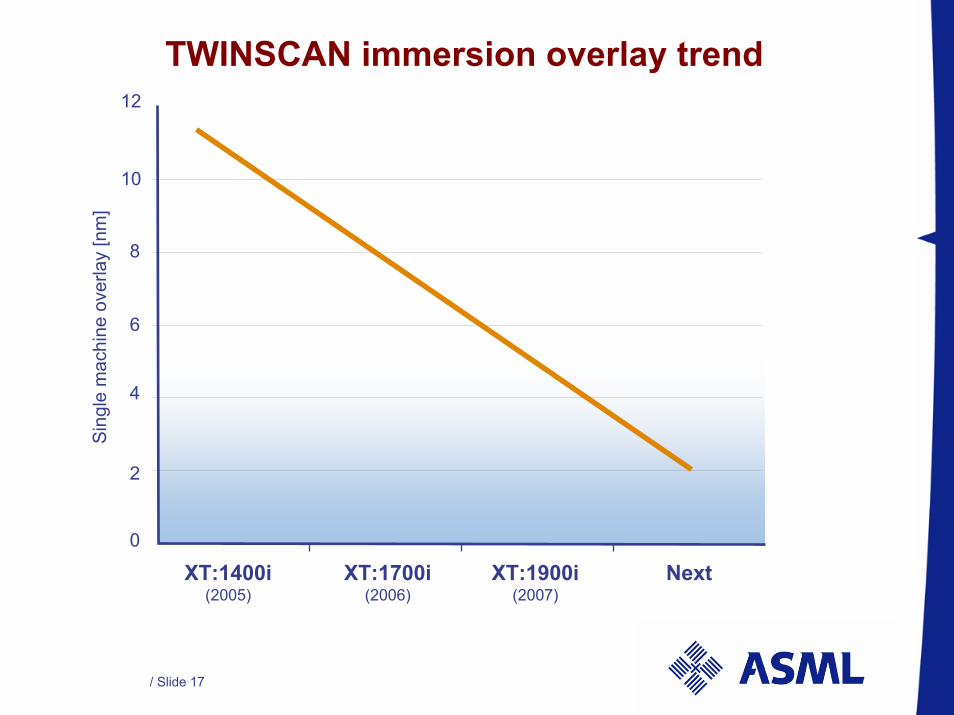
TWINSCAN immersion overlay trend12
10
Sin
gle
mac
hine
ove
rlay
[nm
]
8
6
4
2
0
XT:1400i(2005)
XT:1700i(2006)
XT:1900i(2007)
Next

/ Slide 18
ASML mask and system enhancements extend lithography to the limit of k1
Offline Dual stage wafer height mapping
Focus Dry, Expose Wet
Mask enhancement techniques &
optimization softwareDoseMapper for optimum
CD Uniformity
Flexible off-axis & polarized illumination
Illumination source optimization & software
+ =
Application specific lens setup
In-built wave-front, polarization and pupil metrology
GridMapper for improved Overlay

/ Slide 19
Low k1: High design to wafer integrationLow k1 (<0.4): Integration of design, mask and lithography processes
Design ForManufacturing
DFM
Application Specific
Manufacturing
Design space Manufacturing space
Litho aware design constraints
OPC & RETs: PSM, D
PT,
Scatte
rbars, D
DL verifi
catio
n Application specific tuning
Source-Mask
Optimization
/ Slide 20
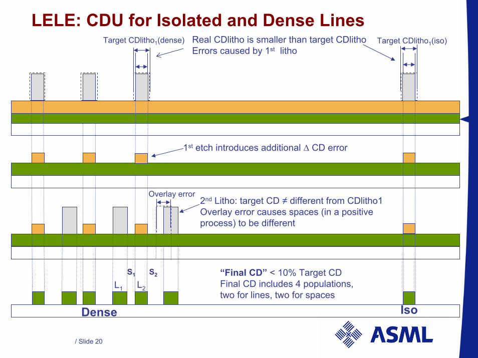
LELE: CDU for Isolated and Dense LinesTarget CDlitho1(dense) Target CDlitho1(iso)
Dense Iso
L1
S1
L2
S2
Real CDlitho is smaller than target CDlithoErrors caused by 1st litho
1st etch introduces additional ∆ CD error
2nd Litho: target CD ≠ different from CDlitho1Overlay error causes spaces (in a positive process) to be different
“Final CD” < 10% Target CDFinal CD includes 4 populations, two for lines, two for spaces
Overlay error

/ Slide 21
10 nm
10 nm
Litho patterning process control for CD and Overlay of 32 nm, using angle-resolved scatterometry
Overlay between litho 1 and 2
DoseMapper recipe
Line1 Line2
Raw etched poly CDU
DoseMapper recipe Optimum GridMapper recipe
DoseMapper corrected etched poly CDU
Mean CD
mean CD
< 4.9 nm < 7.0 nm
< 3.8 nm< 2.8 nm 99.7% OVL X = 3.2 nm 99.7% OVL Y = 3.4 nm
< 0.8 nm
< 6.3 nm 99.7% OVL X = 4.0 nm 99.7% OVL Y = 4.2 nm
Jo Finders et al. | SPIE San Jose, Feb 26, Ref. 6924-07“Double patterning for 32 nm and below, an update”.

/ Slide 22
LFLE: CDU for Isolated and Dense Lines
Target CDlitho1(dense) Target CDlitho1(iso)
Dense Iso
L1
S1
L2
S2
Real CDlitho is smaller than target CDlithoErrors caused by 1st litho
Track freeze process introduces additional ∆ CD error
2nd Litho: target CD ≠ different from CDlitho1Overlay error causes spaces (in a positive process) to be different
“Final CD” < 10% Target CDFinal CD includes 4 populations, two for lines, two for spaces
Overlay error
Wafer does not leave litho cluster
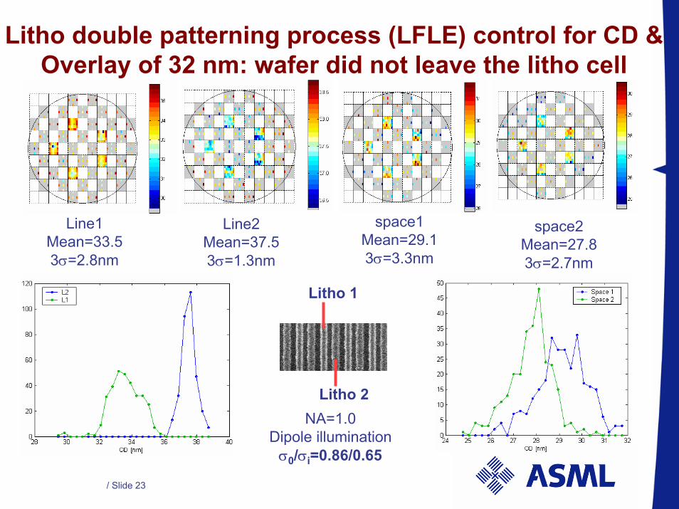
/ Slide 23
Line1Mean=33.53σ=2.8nm
space1Mean=29.13σ=3.3nm
Line2Mean=37.53σ=1.3nm
space2Mean=27.83σ=2.7nm
L1 L2
S1 S2
Litho 1
Litho 2NA=1.0
Dipole illuminationσ0/σi=0.86/0.65
Litho double patterning process (LFLE) control for CD & Overlay of 32 nm: wafer did not leave the litho cell

/ Slide 24
Litho double patterning process (LFLE) control for CD & Overlay of 32 nm: wafer did not leave the litho cell
211
1RL PPP +
=1_DPT OL P P= −
P1RP1L
DPT overlay 3σ<2.5nm

/ Slide 25
Outline
SRAM gate DPT example
− Overlay, CDU, Resolution (Design) trade-off
Spacer Challenges
Litho Improvements to Enable LELE & LFLE DPT
Conclusion

/ Slide 26
ConclusionsSpacer Challenges− Not all designs can benefit from Spacer DPT self-alignment− Burdens the designer or makes design rules overly restrictive− Additional cost/complexity (cycle time) serves as a detractor
Litho Challenges/Improvements− Spacer, LELE & LFLE require much tighter CDU than required from SE
lithography; LELE/LFLE must also achieve overlay on the order 3nm− Intra-layer overlay not as challenging as inter-layer overlay due to
elimination of some process effects.− Tighter CDU and overlay budgets should be achieved through active
compensation of wafer and field spatial distributions− DoseMapper to reduce intra-field and inter-field CDU due to reticle,
track, and etch CD variation− GridMapper to reduce intra-field and inter-field OV due to reticle
registration and wafer distortionXT:1950Hi drives performance improvements to further enable DPT processing. Future improvements planned in productivity, overlay & imaging to enable cost effective lowk1 solutions.

/ Slide 27
Acknowledgement
ASML− Donis Flagello, Jo Finders, Mircea Dusa, Skip Miller, David
Deckers, Ad Lammers, Dorothe Oorschot, Bart Rijpers, Paul de Haas, Christian Leewis, Martyn Coogans, Eddy van derHeijden, John Quaedackers, Jeroen Meessen, Toine de Kort, Joris Kuin, Robert Routh, Andre Engelen, Eelco van Setten, Mark van de Kerkhof, Hans Bakker, Jos de Klerk, Koen van Ingen Schneau, Noreen Harned
IMEC− Mireille Maenhoudt, Shaunee Cheng, Patrick Jaenen, Tom Vandeweyer,
Diziana Vangoidsenhoven
Carl Zeiss− Winfried Kaiser,

/ Slide 28


