Halogen and Antimony Free. “Green” Device (Note 3)
Pin Assignments
(Top View)
1
2
3
4
8
7
6
5
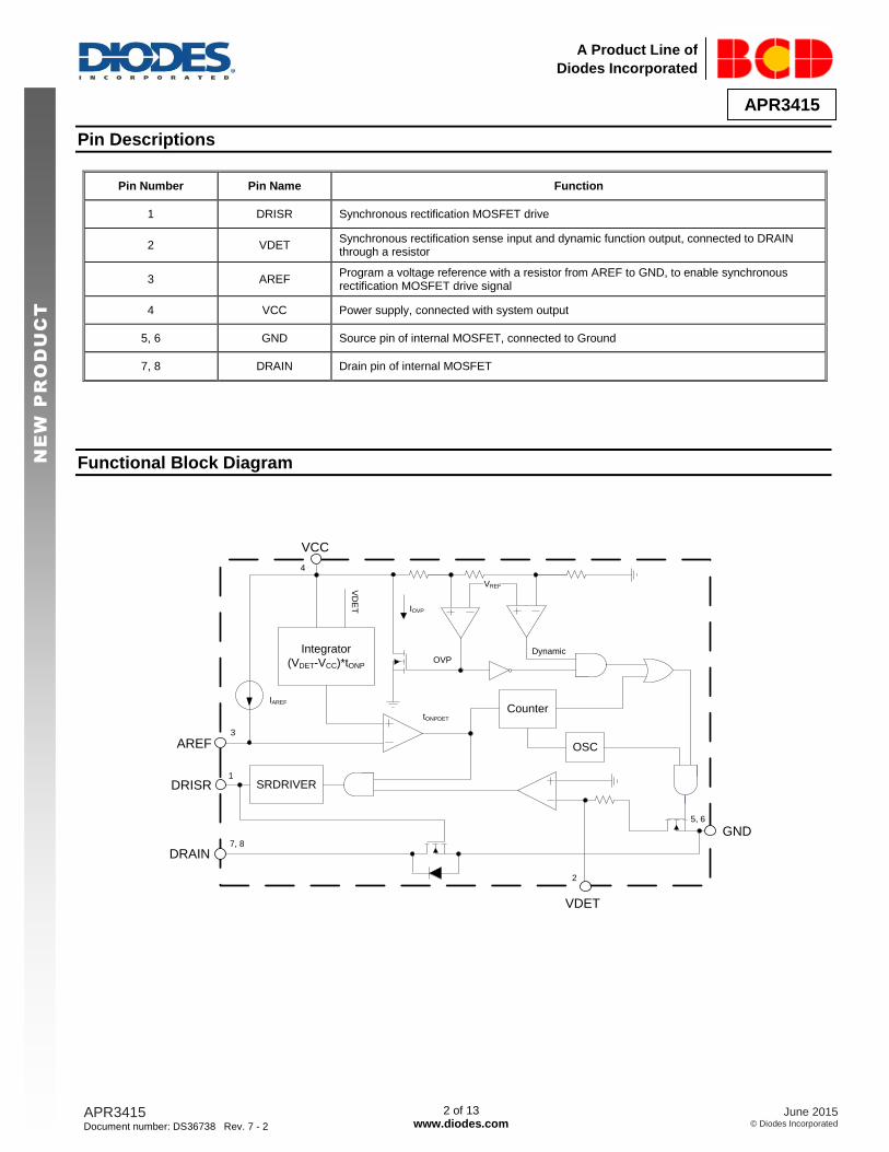
DRISR
VDET
AREF
VCC
DRAIN
DRAIN
GND
GND
SO-8
Applications
• Adapters/Chargers for Cell/Cordless Phones, ADSL Modems, MP3
and Other Portable Apparatus
• Standby and Auxiliary Power Supplies
Notes: 1. No purposely added lead. Fully EU Directive 2002/95/EC (RoHS) & 2011/65/EU (RoHS 2) compliant. 2. See http://www.diodes.com/quality/lead_free.html for more information about Diodes Incorporated’s definitions of Halogen- and Antimony-free, "Green" and Lead-free. 3. Halogen- and Antimony-free "Green” products are defined as those which contain <900ppm bromine, <900ppm chlorine (<1500ppm total Br + Cl) and <1000ppm antimony compounds.
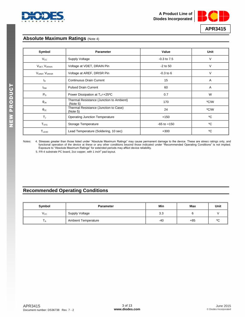
VDET, VDRAIN Voltage at VDET, DRAIN Pin -2 to 50 V
VAREF, VDRISR Voltage at AREF, DRISR Pin -0.3 to 6 V
ID Continuous Drain Current 15 A
IDM Pulsed Drain Current 60 A
PD Power Dissipation at TA=+25ºC 0.7 W
θJA Thermal Resistance (Junction to Ambient) (Note 5)
170 ºC/W
θJC Thermal Resistance (Junction to Case) (Note 5)
24 ºC/W
TJ Operating Junction Temperature +150 ºC
TSTG Storage Temperature -65 to +150 ºC
TLEAD Lead Temperature (Soldering, 10 sec) +300 ºC
Notes: 4. Stresses greater than those listed under “Absolute Maximum Ratings” may cause permanent damage to the device. These are stress ratings only, and
functional operation of the device at these or any other conditions beyond those indicated under “Recommended Operating Conditions” is not implied. Exposure to “Absolute Maximum Ratings” for extended periods may affect device reliability.
5. FR-4 substrate PC board, 2oz copper, with 1 inch2 pad layout.
When the controlled MOSFET gate is turned on, some ringing noise is generated. The minimum on-time timer blanks the VTHOFF comparator,
keeping the controlled MOSFET on for at least the minimum on time. If VTHOFF falls below the threshold before minimum on time expires, the
MOSFET will keep on until the end of the minimum on time.
The minimum on time is in direct proportion to the (VDET-VCC)*tONP. When (VDET-VCC)*tONP=5V*5μs, the minimum on time is about 1.8μs.
The Value and Meaning of AREF Resistor
As to DCM operation Flyback converter, after secondary rectifier stops conduction the primary MOSFET Drain-to-source ringing waveform is
resulted from the resonant of primary inductance and equivalent switch device output capacitance. This ringing waveform probably leads to
Synchronous Rectifier error conduction. To avoid this fault happening, APR3415 has a special function design by means of volt-second product
detecting. From the sensed voltage of VDET pin to see, the volt-second product of voltage above VCC at primary switch on time is much higher
than the volt-second product of each cycle ringing voltage above VCC. Therefore, before every time Synchronous Rectifier turning on, APR3415
judges if the detected volt-second product of VDET voltage above VCC is higher than a threshold and then turn on synchronous Rectifier. The
purpose of AREF resistor is to determine the volt-second product threshold. APR3415 has a parameter, Kqs, which converts RAREF value to volt-
second product.
Kqs*R2Area AREF
In general, Area1 and Area3, the value of which should be test on system, depend on system design and always are fixed after system design
frozen. As to BCD PSR design, the Area1 value changes with primary peak current value and Area3 value generally keeps constant at all of
conditions. So the AREF resistor design should consider the worst case, the minimum primary peak current condition. Since of system design
parameter distribution, Area1 and Area3 have moderate tolerance. So Area2 should be designed between the middle of Area1 and Area3 to keep
enough design margin.
Area1Kqs*R3Area AREF
VDET
VCC
Area3
Area1=(VDET-VCC)*tONP
Area2=Kqs*RAREF
Figure 3. AREF Function
SR Minimum Operating Voltage
APR3415 sets a minimum SR operating voltage by comparing the difference between VDET and output voltage (VCC). The value of VDET–VCC must
be higher than its internal reference, then APR3415 will begin to integrate the area of (VDET–VCC)*tONP. If not, the area integrating will not begin and
the SR driver will be disabled.
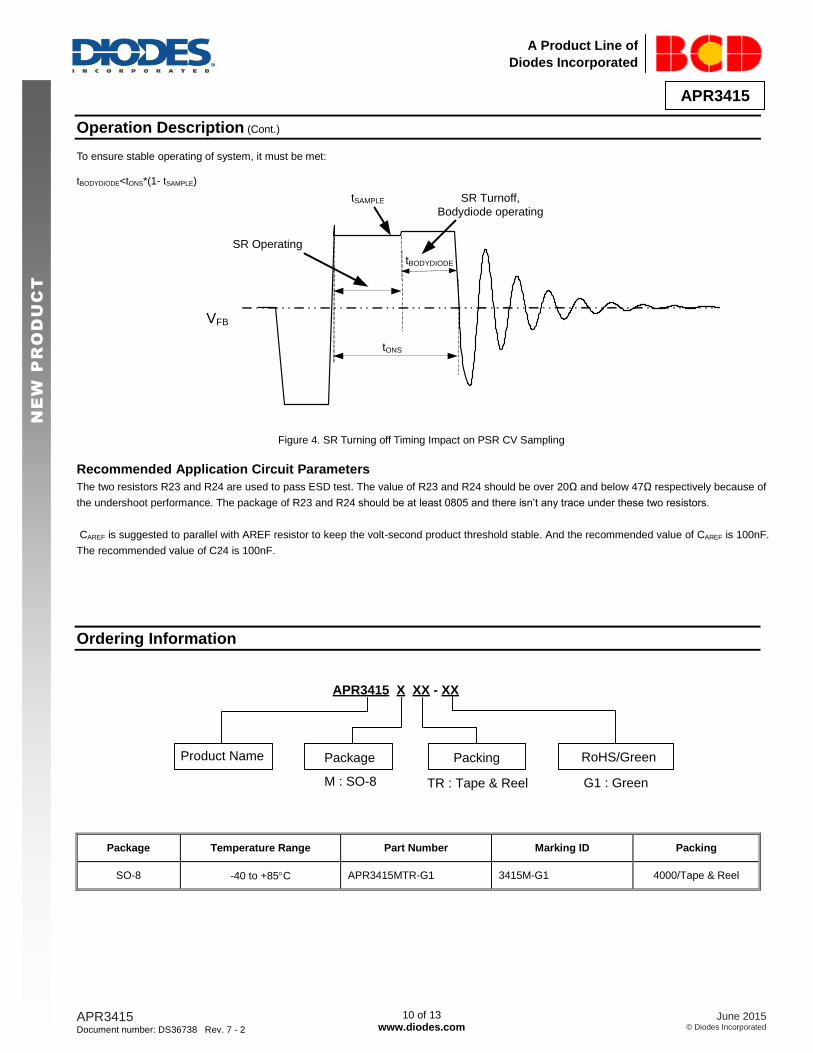
SR Turning off Timing Impact on PSR CV Sampling
As to synchronous rectification on Flyback power system, SR MOSFET need to turn off in advance of secondary side current decreasing to zero to
avoid current flowing reversely. When SR turns off in advance, the secondary current will flow through the body diode. The SR turning off time is
determined by the VTHOFF at a fixed system. When VTHOFF is more close to zero, the SR turning on time gets longer and body diode conduction time
gets shorter. Since of the different voltage drop between SR MOSFET and body diode, the PSR feedback signal VFB appears a voltage jump at the
time of SR MOSFET turning off. If the PSR CV sampling time tSAMPLE is close to even behind this voltage jump time, there will be system unstable
operation issue or the lower output voltage issue.
IMPORTANT NOTICE DIODES INCORPORATED MAKES NO WARRANTY OF ANY KIND, EXPRESS OR IMPLIED, WITH REGARDS TO THIS DOCUMENT, INCLUDING, BUT NOT LIMITED TO, THE IMPLIED WARRANTIES OF MERCHANTABILITY AND FITNESS FOR A PARTICULAR PURPOSE (AND THEIR EQUIVALENTS UNDER THE LAWS OF ANY JURISDICTION). Diodes Incorporated and its subsidiaries reserve the right to make modifications, enhancements, improvements, corrections or other changes without further notice to this document and any product described herein. Diodes Incorporated does not assume any liability arising out of the application or use of this document or any product described herein; neither does Diodes Incorporated convey any license under its patent or trademark rights, nor the rights of others. Any Customer or user of this document or products described herein in such applications shall assume all risks of such use and will agree to hold Diodes Incorporated and all the companies whose products are represented on Diodes Incorporated website, harmless against all damages. Diodes Incorporated does not warrant or accept any liability whatsoever in respect of any products purchased through unauthorized sales channel. Should Customers purchase or use Diodes Incorporated products for any unintended or unauthorized application, Customers shall indemnify and hold Diodes Incorporated and its representatives harmless against all claims, damages, expenses, and attorney fees arising out of, directly or indirectly, any claim of personal injury or death associated with such unintended or unauthorized application. Products described herein may be covered by one or more United States, international or foreign patents pending. Product names and markings noted herein may also be covered by one or more United States, international or foreign trademarks. This document is written in English but may be translated into multiple languages for reference. Only the English version of this document is the final and determinative format released by Diodes Incorporated.
LIFE SUPPORT Diodes Incorporated products are specifically not authorized for use as critical components in life support devices or systems without the express written approval of the Chief Executive Officer of Diodes Incorporated. As used herein: A. Life support devices or systems are devices or systems which: 1. are intended to implant into the body, or
2. support or sustain life and whose failure to perform when properly used in accordance with instructions for use provided in the labeling can be reasonably expected to result in significant injury to the user.