+ ± + ± DAC DAC DRV632 RIGHT LEFT Product Folder Sample & Buy Technical Documents Tools & Software Support & Community DRV632 SLOS681B – JANUARY 2011 – REVISED AUGUST 2015 DRV632 DirectPath™, 2-VRMS Audio Line Driver With Adjustable Gain 1 Features 3 Description The DRV632 is a 2-V RMS pop-free stereo line driver 1• Stereo DirectPath™ Audio Line Driver designed to allow the removal of the output dc- – 2 Vrms Into 10 kΩ With 3.3-V Supply blocking capacitors for reduced component count and • Low THD+N < 0.01% at 2 Vrms Into 10 kΩ cost. The device is ideal for single-supply electronics where size and cost are critical design parameters. • High SNR, >90 dB • 600-Ω Output Load Compliant Designed using TI’s patented DirectPath™ technology, The DRV632 is capable of driving 2 V RMS • Differential Input and Single-Ended Output into a 10-kΩ load with 3.3-V supply voltage. The • Adjustable Gain by External Gain-Setting device has differential inputs and uses external gain- Resistors setting resistors to support a gain range of ±1 V/V to • Low DC Offset, <1 mV ±10 V/V, and gain can be configured individually for each channel. Line outputs have ±8-kV IEC ESD • Ground-Referenced Outputs Eliminate DC- protection, requiring just a simple resistor-capacitor Blocking Capacitors ESD protection circuit. The DRV632 has built-in – Reduce Board Area active-mute control for pop-free audio on/off control. – Reduce Component Cost The DRV632 has an external undervoltage detector that mutes the output when the power supply is – Improve THD+N Performance removed, ensuring a pop-free shutdown. – No Degradation of Low-Frequency Response Using the DRV632 in audio products can reduce Due to Output Capacitors component count considerably compared to • Short-Circuit Protection traditional methods of generating a 2-V RMS output. • Click- and Pop-Reduction Circuitry The DRV632 does not require a power supply greater • External Undervoltage Mute than 3.3 V to generate its 5.6-V pp output, nor does it require a split-rail power supply. The DRV632 • Active Mute Control for Pop-Free Audio On/Off integrates its own charge pump to generate a Control negative supply rail that provides a clean, pop-free • Space-Saving TSSOP Package ground-biased 2-V RMS output. The DRV632 is available in a 14-pin TSSOP. 2 Applications • Set-Top Boxes Device Information (1) • Blu-ray Disc™, DVD Players PART NUMBER PACKAGE BODY SIZE (NOM) • LCD and PDP TV DRV632 TSSOP (14) 5.00 mm × 4.40 mm • Mini/Micro Combo Systems (1) For all available packages, see the orderable addendum at the end of the datasheet. • Sound Cards • Laptops Simplified Diagram 1 An IMPORTANT NOTICE at the end of this data sheet addresses availability, warranty, changes, use in safety-critical applications, intellectual property matters and other important disclaimers. PRODUCTION DATA.
Transcript
+
±
+
±
DAC
DAC
DRV632
RIGHT
LEFT
Product
Folder
Sample &Buy
Technical
Documents
Tools &
Software
Support &Community
DRV632SLOS681B –JANUARY 2011–REVISED AUGUST 2015
DRV632 DirectPath™, 2-VRMS Audio Line Driver With Adjustable Gain1 Features 3 Description
The DRV632 is a 2-VRMS pop-free stereo line driver1• Stereo DirectPath™ Audio Line Driver
designed to allow the removal of the output dc-– 2 Vrms Into 10 kΩ With 3.3-V Supply blocking capacitors for reduced component count and• Low THD+N < 0.01% at 2 Vrms Into 10 kΩ cost. The device is ideal for single-supply electronics
where size and cost are critical design parameters.• High SNR, >90 dB• 600-Ω Output Load Compliant Designed using TI’s patented DirectPath™
technology, The DRV632 is capable of driving 2 VRMS• Differential Input and Single-Ended Outputinto a 10-kΩ load with 3.3-V supply voltage. The• Adjustable Gain by External Gain-Setting device has differential inputs and uses external gain-Resistors setting resistors to support a gain range of ±1 V/V to
• Low DC Offset, <1 mV ±10 V/V, and gain can be configured individually foreach channel. Line outputs have ±8-kV IEC ESD• Ground-Referenced Outputs Eliminate DC-protection, requiring just a simple resistor-capacitorBlocking CapacitorsESD protection circuit. The DRV632 has built-in– Reduce Board Area active-mute control for pop-free audio on/off control.
– Reduce Component Cost The DRV632 has an external undervoltage detectorthat mutes the output when the power supply is– Improve THD+N Performanceremoved, ensuring a pop-free shutdown.– No Degradation of Low-Frequency ResponseUsing the DRV632 in audio products can reduceDue to Output Capacitorscomponent count considerably compared to• Short-Circuit Protectiontraditional methods of generating a 2-VRMS output.
• Click- and Pop-Reduction Circuitry The DRV632 does not require a power supply greater• External Undervoltage Mute than 3.3 V to generate its 5.6-Vpp output, nor does it
require a split-rail power supply. The DRV632• Active Mute Control for Pop-Free Audio On/Offintegrates its own charge pump to generate aControlnegative supply rail that provides a clean, pop-free• Space-Saving TSSOP Package ground-biased 2-VRMS output.
The DRV632 is available in a 14-pin TSSOP.2 Applications• Set-Top Boxes Device Information(1)
• Blu-ray Disc™, DVD Players PART NUMBER PACKAGE BODY SIZE (NOM)• LCD and PDP TV DRV632 TSSOP (14) 5.00 mm × 4.40 mm• Mini/Micro Combo Systems (1) For all available packages, see the orderable addendum at
the end of the datasheet.• Sound Cards• Laptops
Simplified Diagram
1
An IMPORTANT NOTICE at the end of this data sheet addresses availability, warranty, changes, use in safety-critical applications,intellectual property matters and other important disclaimers. PRODUCTION DATA.
Changes from Original (January 2011) to Revision A Page
• Changed description of UVP in PIN FUNCTIONS table ........................................................................................................ 4• Deleted min value for SNR and DNR in OPERATING CHARACTERISTICS table ............................................................... 6
DRV632SLOS681B –JANUARY 2011–REVISED AUGUST 2015 www.ti.com
6 Pin Configuration and Functions
PW Package14-Pin TSSOP
(Top View)
Pin FunctionsPIN
TYPE (1) DESCRIPTIONNAME NO.CN 7 I/O Charge-pump flying capacitor negative connectionCP 8 I/O Charge-pump flying capacitor positive connectionGND 4, 10 P Ground–INL 13 I Left-channel OPAMP negative input+INL 14 I Left-channel OPAMP positive input–INR 2 I Right-channel OPAMP negative input+INR 1 I Right-channel OPAMP positive inputMute 5 I Mute, active-lowOUTL 12 O Left-channel OPAMP outputOUTR 3 O Right-channel OPAMP outputUVP 11 I Undervoltage protection, internal pullup; unconnected if UVP function is unused.VDD 9 P Positive supplyVSS 6 P Supply voltage
(1) I = input, O = output, P = power
7 Specifications
7.1 Absolute Maximum Ratingsover operating free-air temperature range (1)
MIN MAX UNITSupply voltage, VDD to GND –0.3 4 V
VI Input voltage VSS – 0.3 VDD + 0.3 VRL Minimum load impedance – line outputs – OUTL, OUTR 600 Ω
Mute to GND, UVP to GND –0.3 VDD + 0.3 VTJ Maximum operating junction temperature –40 150 °CTstg Storage temperature –40 150 °C
(1) Stresses beyond those listed under Absolute Maximum Ratings may cause permanent damage to the device. These are stress ratingsonly, and functional operation of the device at these or any other conditions beyond those indicated under Recommended OperatingConditions is not implied. Exposure to absolute-maximum-rated conditions for extended periods may affect device reliability.
DRV632www.ti.com SLOS681B –JANUARY 2011–REVISED AUGUST 2015
7.2 ESD RatingsVALUE UNIT
Human body model (HBM), per ANSI/ESDA/JEDEC JS-001 (1) ±1500V(ESD) Electrostatic discharge VCharged-device model (CDM), per JEDEC specification JESD22- ±4000
C101 (2)
(1) JEDEC document JEP155 states that 500-V HBM allows safe manufacturing with a standard ESD control process.(2) JEDEC document JEP157 states that 250-V CDM allows safe manufacturing with a standard ESD control process.
7.3 Recommended Operating ConditionsMIN NOM MAX UNIT
VDD Supply voltage DC supply voltage 3 3.3 3.6 VRL Load impedance 0.6 10 kΩVIL Low-level input voltage Mute 40 % of VDDVIH High-level input voltage Mute 60 % of VDDTA Operating free-air temperature –40 25 85 °C
PARAMETER TEST CONDITIONS MIN TYP MAX UNIT|VOS| Output offset voltage VDD = 3.3 V 0.5 1 mVPSRR Power-supply rejection ratio 80 dBVOH High-level output voltage VDD = 3.3 V 3.1 VVOL Low-level output voltage VDD = 3.3 V –3.0 V
5VUVP_EX External UVP detect voltage 1.25 VVUVP_EX_HYSTERESIS External UVP detect hysteresis current 5 µAfCP Charge pump switching frequency 200 300 400 kHz|IIH| High-level input current, Mute VDD = 3.3 V, VIH = VDD 1 µA|IIL| Low-level input current, Mute VDD = 3.3 V, VIL = 0 V 1 µA
VDD = 3.3 V, no load, Mute = VDD 5 14 25IDD Supply current mAVDD = 3.3 V, no load, Mute = GND, 14
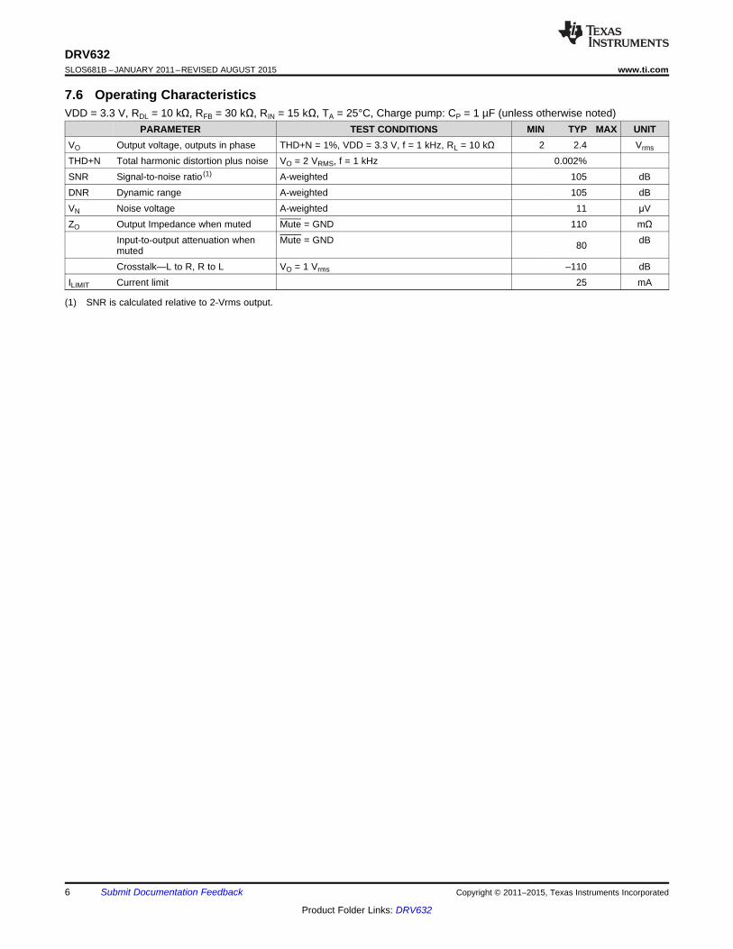
PARAMETER TEST CONDITIONS MIN TYP MAX UNITVO Output voltage, outputs in phase THD+N = 1%, VDD = 3.3 V, f = 1 kHz, RL = 10 kΩ 2 2.4 Vrms
THD+N Total harmonic distortion plus noise VO = 2 VRMS, f = 1 kHz 0.002%SNR Signal-to-noise ratio (1) A-weighted 105 dBDNR Dynamic range A-weighted 105 dBVN Noise voltage A-weighted 11 μVZO Output Impedance when muted Mute = GND 110 mΩ
Input-to-output attenuation when Mute = GND dB80mutedCrosstalk—L to R, R to L VO = 1 Vrms –110 dB
DRV632SLOS681B –JANUARY 2011–REVISED AUGUST 2015 www.ti.com
9 Detailed Description
9.1 OverviewCombining the TI's patented DirectPath technology with the built-in click and pop reduction circuit, the DRV632 isa 2-VRMS pop-free stereo line driver designed to avoid the use of the output DC-blocking capacitors, resulting inreduced component count and cost. The DRV632 is capable of driving 2-VRMS into a line load of 600 Ω to 10kΩ with a 3.3-V supply voltage. The use of charge-pump flying, PVSS, and decoupling capacitors ensure theperformance of the amplifier. The device has two channels with differential inputs that require DC input-blockingcapacitors to block the DC portion of the audio source. These allow the DRV632 inputs to be properly biased toprovide maximum performance. The DRV632 allows external gain-setting resistors to support a gain range of ±1V/V to ±10 V/V. The gain can be configured individually for each channel. Additionally, both channels can beused as a second-order filter when the removal of out-of-band noise is required. The DRV632 has a built-inactive-mute control for pop-free audio on/off, and avoids the click and pop generation by using externalundervoltage detection. The device does not generate a pop or click when the power supply is removed orplaced.
DRV632www.ti.com SLOS681B –JANUARY 2011–REVISED AUGUST 2015
9.3 Feature Description
9.3.1 Line Driver AmplifiersSingle-supply line-driver amplifiers typically require dc-blocking capacitors. The top drawing in Figure 6 illustratesthe conventional line-driver amplifier connection to the load and output signal. DC blocking capacitors are oftenlarge in value. The line load (typical resistive values of 600 Ω to 10 kΩ) combines with the dc blocking capacitorsto form a high-pass filter. Equation 1 shows the relationship between the load impedance (RL), the capacitor(CO), and the cutoff frequency (fC).
(1)
CO can be determined using Equation 2, where the load impedance and the cutoff frequency are known.
(2)
If fC is low, the capacitor must then have a large value because the load resistance is small. Large capacitancevalues require large package sizes. Large package sizes consume PCB area, stand high above the PCB,increase cost of assembly, and can reduce the fidelity of the audio output signal.
Figure 6. Conventional and DirectPath Line Drivers
The DirectPath amplifier architecture operates from a single supply but makes use of an internal charge pump toprovide a negative voltage rail. Combining the user-provided positive rail and the negative rail generated by theIC, the device operates in what is effectively a split-supply mode. The output voltages are now centered at zerovolts with the capability to swing to the positive rail or negative rail. Combining this with the built-in click and popreduction circuit, the DirectPath amplifier requires no output dc blocking capacitors. The bottom block diagramand waveform of Figure 6 illustrate the ground-referenced line-driver architecture. This is the architecture of theDRV632.
9.3.2 Charge-Pump Flying Capacitor and PVSS CapacitorThe charge-pump flying capacitor serves to transfer charge during the generation of the negative supply voltage.The PVSS capacitor must be at least equal to the charge-pump capacitor in order to allow maximum chargetransfer. Low-ESR capacitors are an ideal selection, and a value of 1 μF is typical. Capacitor values that aresmaller than 1 μF can be used, but the maximum output voltage may be reduced and the device may notoperate to specifications. If the DRV632 is used in highly noise-sensitive circuits, TI recommends adding a smallLC filter on the VDD connection.
DRV632SLOS681B –JANUARY 2011–REVISED AUGUST 2015 www.ti.com
Feature Description (continued)9.3.3 Decoupling CapacitorsThe DRV632 is a DirectPath line-driver amplifier that requires adequate power supply decoupling to ensure thatthe noise and total harmonic distortion (THD) are low. A good, low equivalent-series-resistance (ESR) ceramiccapacitor, typically 1 μF, placed as close as possible to the device VDD lead works best. Placing this decouplingcapacitor close to the DRV632 is important for the performance of the amplifier. For filtering lower-frequencynoise signals, a 10-μF or greater capacitor placed near the audio power amplifier would also help, but it is notrequired in most applications because of the high PSRR of this device.
9.3.4 Gain-Setting Resistor RangesThe gain-setting resistors, RIN and Rfb, must be chosen so that noise, stability, and input capacitor size of theDRV632 are kept within acceptable limits. Voltage gain is defined as Rfb divided by RIN.
Selecting values that are too low demands a large input ac-coupling capacitor, CIN. Selecting values that are toohigh increases the noise of the amplifier. Table 1 lists the recommended resistor values for different inverting-input gain settings.
9.3.5 Input-Blocking CapacitorsDC input-blocking capacitors are required to be added in series with the audio signal into the input pins of theDRV632. These capacitors block the dc portion of the audio source and allow the DRV632 inputs to be properlybiased to provide maximum performance.
These capacitors form a high-pass filter with the input resistor, RIN. The cutoff frequency is calculated usingEquation 3. For this calculation, the capacitance used is the input-blocking capacitor, and the resistance is theinput resistor chosen from Table 1; then the frequency and/or capacitance can be determined when one of thetwo values is given.
It is recommended to use electrolytic capacitors or high-voltage-rated capacitors as input blocking capacitors toensure minimal variation in capacitance with input voltages. Such variation in capacitance with input voltages iscommonly seen in ceramic capacitors and can increase low-frequency audio distortion.
(3)
9.3.6 DRV632 UVP OperationThe shutdown threshold at the UVP pin is 1.25 V. The customer must use a resistor divider to obtain theshutdown threshold and hysteresis desired for a particular application. The customer-selected thresholds can bedetermined as follows:
9.3.7 External Undervoltage DetectionExternal undervoltage detection can be used to mute/shut down the DRV632 before an input device cangenerate a pop.
The shutdown threshold at the UVP pin is 1.25 V. The user selects a resistor divider to obtain the shutdownthreshold and hysteresis for the specific application. The thresholds can be determined as follows:
DRV632www.ti.com SLOS681B –JANUARY 2011–REVISED AUGUST 2015
Figure 7. UVP Resistor Divider
9.4 Device Functional Modes
9.4.1 Using the DRV632 as a Second-Order FilterSeveral audio DACs used today require an external low-pass filter to remove out-of-band noise. This is possiblewith the DRV632, as it can be used like a standard operational amplifier. Several filter topologies can beimplemented, both single-ended and differential. In Figure 8, multi-feedback (MFB) with differential input andsingle-ended input are shown.
An ac-coupling capacitor to remove dc content from the source is shown; it serves to block any dc content fromthe source and lowers the dc gain to 1, helping to reduce the output dc offset to a minimum.
To calculate the component values, use the TI WEBENCH® Filter Designer (www.ti.com/filterdesigner).
Figure 8. Second-Order Active Low-Pass Filter
The resistor values should have a low value for obtaining low noise, but should also have a high enough value toget a small-size ac-coupling capacitor. With the proposed values of R1 = 15 kΩ, R2 = 30 kΩ, and R3 = 43 kΩ, adynamic range (DYR) of 106 dB can be achieved with a 1-μF input ac-coupling capacitor.
9.4.2 Mute ModeThe DRV632 can be muted using the low-active Mute pin (pin 5). The click-and-pop suppression capacityensures that when the mute mode is used, it does not generate an additional click or pop.
DRV632SLOS681B –JANUARY 2011–REVISED AUGUST 2015 www.ti.com
10 Application and Implementation
NOTEInformation in the following applications sections is not part of the TI componentspecification, and TI does not warrant its accuracy or completeness. TI’s customers areresponsible for determining suitability of components for their purposes. Customers shouldvalidate and test their design implementation to confirm system functionality.
10.1 Application InformationThis typical connection diagram highlights the required external components and system-level connections forproper operation of the device. This configuration can be realized using the Evaluation Module (EVM) of thedevice. This flexible module allows full evaluation of the device in all available modes of operation. Also see theDRV632 product page for information on ordering the EVM.
DRV632www.ti.com SLOS681B –JANUARY 2011–REVISED AUGUST 2015
Typical Application (continued)10.2.1 Design RequirementsIn this design example, use the parameters listed in Table 2.
Table 2. Design ParametersKEY PARAMETERS VALUE
Supply Voltage 3.3 VSupply Current 0.10 A
Load Impedance 600 Ω (minimum)
10.2.2 Detailed Design Procedure
10.2.2.1 Charge-Pump Flying, PVSS and Decoupling CapacitorsTo transfer charge during the generation of the negative supply voltage, an 1-µF low equivalent-series-resistance(ESR) charge-pump flying capacitor is used for this design. Similar 1-µF capacitors are placed in VSS, and asclose as possible to VDD. See Charge-Pump Flying Capacitor and PVSS Capacitor and Decoupling Capacitorsfor details.
10.2.2.2 Second-Order Active Low-Pass FiltersWith the help of the TI WEBENCH Filter Designer (www.ti.com/filterdesigner), the values of R1 = 15 kΩ, R2 = 30kΩ, R3 = 43 kΩ, C1 = 47 pF, and C2 = 180 pF are proposed to design a second-order low-pass filter with adifferential-input and a single-ended output. See Using the DRV632 as a Second-Order Filter for details.
10.2.2.3 UVP Resistor DividerR11 and R12 are placed to design a resistor divider. The shutdown threshold at the UVP pin is 1.25 V. SeeExternal Undervoltage Detection for details.
10.2.3 Application Curves
Figure 10. Total Harmonic Distortion and Noise vs Output Figure 11. Total Harmonic Distortion and Noise vs OutputVoltage Voltage
DRV632SLOS681B –JANUARY 2011–REVISED AUGUST 2015 www.ti.com
Figure 12. Total Harmonic Distortion and Noise vs Figure 13. Total Harmonic Distortion and Noise vsFrequency Frequency
Figure 14. Crosstalk vs Frequency
11 Power Supply RecommendationsThe device is designed to operate from an input voltage supply range between 3 V and 3.6 V. This input supplymust be well-regulated. If the input supply is located more than a few inches from the DRV632 device, additionalbulk capacitance may be required in addition to the ceramic bypass capacitors. An electrolytic capacitor with avalue of 47 µF is a typical choice.
Placing a decoupling capacitor close to the DRV632 improves the performance of the line-driver amplifier. An lowequivalent-series-resistance (ESR) ceramic capacitor with a value of 1 µF is a typical choice.
If the DRV632 is used in highly noise-sensitive circuits, TI recommends adding a small LC filter on the VDDconnection.
DRV632www.ti.com SLOS681B –JANUARY 2011–REVISED AUGUST 2015
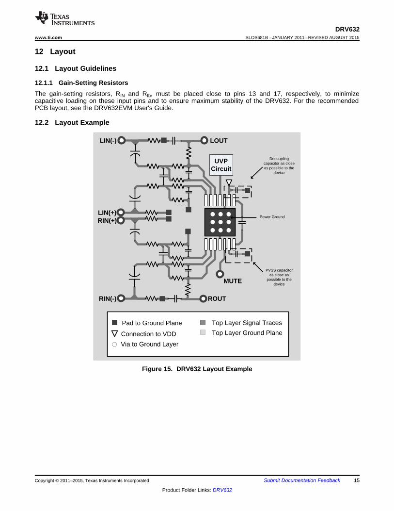
12 Layout
12.1 Layout Guidelines
12.1.1 Gain-Setting ResistorsThe gain-setting resistors, RIN and Rfb, must be placed close to pins 13 and 17, respectively, to minimizecapacitive loading on these input pins and to ensure maximum stability of the DRV632. For the recommendedPCB layout, see the DRV632EVM User's Guide.
DRV632SLOS681B –JANUARY 2011–REVISED AUGUST 2015 www.ti.com
13 Device and Documentation Support
13.1 Device Support
13.1.1 Development SupportFor the DRV632EVM and Gerber files, go to www.ti.com/tool/DRV632EVM.
13.2 Community ResourcesThe following links connect to TI community resources. Linked contents are provided "AS IS" by the respectivecontributors. They do not constitute TI specifications and do not necessarily reflect TI's views; see TI's Terms ofUse.
TI E2E™ Online Community TI's Engineer-to-Engineer (E2E) Community. Created to foster collaborationamong engineers. At e2e.ti.com, you can ask questions, share knowledge, explore ideas and helpsolve problems with fellow engineers.
Design Support TI's Design Support Quickly find helpful E2E forums along with design support tools andcontact information for technical support.
13.3 TrademarksDirectPath, E2E are trademarks of Texas Instruments.WEBENCH is a registered trademark of Texas Instruments.Blu-ray Disc is a trademark of Blu-ray Disc Association.All other trademarks are the property of their respective owners.
13.4 Electrostatic Discharge CautionThese devices have limited built-in ESD protection. The leads should be shorted together or the device placed in conductive foamduring storage or handling to prevent electrostatic damage to the MOS gates.
13.5 GlossarySLYZ022 — TI Glossary.
This glossary lists and explains terms, acronyms, and definitions.
14 Mechanical, Packaging, and Orderable InformationThe following pages include mechanical, packaging, and orderable information. This information is the mostcurrent data available for the designated devices. This data is subject to change without notice and revision ofthis document. For browser-based versions of this data sheet, refer to the left-hand navigation.
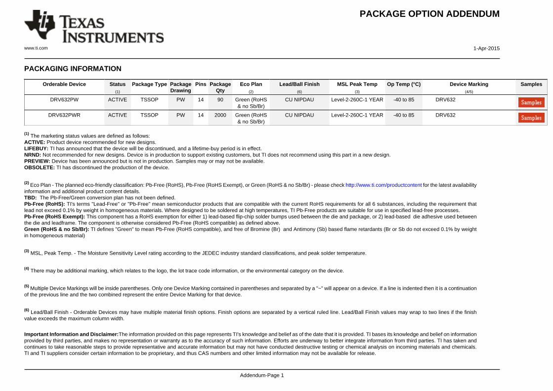
DRV632PW ACTIVE TSSOP PW 14 90 Green (RoHS& no Sb/Br)
CU NIPDAU Level-2-260C-1 YEAR -40 to 85 DRV632
DRV632PWR ACTIVE TSSOP PW 14 2000 Green (RoHS& no Sb/Br)
CU NIPDAU Level-2-260C-1 YEAR -40 to 85 DRV632
(1) The marketing status values are defined as follows:ACTIVE: Product device recommended for new designs.LIFEBUY: TI has announced that the device will be discontinued, and a lifetime-buy period is in effect.NRND: Not recommended for new designs. Device is in production to support existing customers, but TI does not recommend using this part in a new design.PREVIEW: Device has been announced but is not in production. Samples may or may not be available.OBSOLETE: TI has discontinued the production of the device.
(2) Eco Plan - The planned eco-friendly classification: Pb-Free (RoHS), Pb-Free (RoHS Exempt), or Green (RoHS & no Sb/Br) - please check http://www.ti.com/productcontent for the latest availabilityinformation and additional product content details.TBD: The Pb-Free/Green conversion plan has not been defined.Pb-Free (RoHS): TI's terms "Lead-Free" or "Pb-Free" mean semiconductor products that are compatible with the current RoHS requirements for all 6 substances, including the requirement thatlead not exceed 0.1% by weight in homogeneous materials. Where designed to be soldered at high temperatures, TI Pb-Free products are suitable for use in specified lead-free processes.Pb-Free (RoHS Exempt): This component has a RoHS exemption for either 1) lead-based flip-chip solder bumps used between the die and package, or 2) lead-based die adhesive used betweenthe die and leadframe. The component is otherwise considered Pb-Free (RoHS compatible) as defined above.Green (RoHS & no Sb/Br): TI defines "Green" to mean Pb-Free (RoHS compatible), and free of Bromine (Br) and Antimony (Sb) based flame retardants (Br or Sb do not exceed 0.1% by weightin homogeneous material)
(3) MSL, Peak Temp. - The Moisture Sensitivity Level rating according to the JEDEC industry standard classifications, and peak solder temperature.
(4) There may be additional marking, which relates to the logo, the lot trace code information, or the environmental category on the device.
(5) Multiple Device Markings will be inside parentheses. Only one Device Marking contained in parentheses and separated by a "~" will appear on a device. If a line is indented then it is a continuationof the previous line and the two combined represent the entire Device Marking for that device.
(6) Lead/Ball Finish - Orderable Devices may have multiple material finish options. Finish options are separated by a vertical ruled line. Lead/Ball Finish values may wrap to two lines if the finishvalue exceeds the maximum column width.
Important Information and Disclaimer:The information provided on this page represents TI's knowledge and belief as of the date that it is provided. TI bases its knowledge and belief on informationprovided by third parties, and makes no representation or warranty as to the accuracy of such information. Efforts are underway to better integrate information from third parties. TI has taken andcontinues to take reasonable steps to provide representative and accurate information but may not have conducted destructive testing or chemical analysis on incoming materials and chemicals.TI and TI suppliers consider certain information to be proprietary, and thus CAS numbers and other limited information may not be available for release.
In no event shall TI's liability arising out of such information exceed the total purchase price of the TI part(s) at issue in this document sold by TI to Customer on an annual basis.
Texas Instruments Incorporated (TI) reserves the right to make corrections, enhancements, improvements and other changes to itssemiconductor products and services per JESD46, latest issue, and to discontinue any product or service per JESD48, latest issue. Buyersshould obtain the latest relevant information before placing orders and should verify that such information is current and complete.TI’s published terms of sale for semiconductor products (http://www.ti.com/sc/docs/stdterms.htm) apply to the sale of packaged integratedcircuit products that TI has qualified and released to market. Additional terms may apply to the use or sale of other types of TI products andservices.Reproduction of significant portions of TI information in TI data sheets is permissible only if reproduction is without alteration and isaccompanied by all associated warranties, conditions, limitations, and notices. TI is not responsible or liable for such reproduceddocumentation. Information of third parties may be subject to additional restrictions. Resale of TI products or services with statementsdifferent from or beyond the parameters stated by TI for that product or service voids all express and any implied warranties for theassociated TI product or service and is an unfair and deceptive business practice. TI is not responsible or liable for any such statements.Buyers and others who are developing systems that incorporate TI products (collectively, “Designers”) understand and agree that Designersremain responsible for using their independent analysis, evaluation and judgment in designing their applications and that Designers havefull and exclusive responsibility to assure the safety of Designers' applications and compliance of their applications (and of all TI productsused in or for Designers’ applications) with all applicable regulations, laws and other applicable requirements. Designer represents that, withrespect to their applications, Designer has all the necessary expertise to create and implement safeguards that (1) anticipate dangerousconsequences of failures, (2) monitor failures and their consequences, and (3) lessen the likelihood of failures that might cause harm andtake appropriate actions. Designer agrees that prior to using or distributing any applications that include TI products, Designer willthoroughly test such applications and the functionality of such TI products as used in such applications.TI’s provision of technical, application or other design advice, quality characterization, reliability data or other services or information,including, but not limited to, reference designs and materials relating to evaluation modules, (collectively, “TI Resources”) are intended toassist designers who are developing applications that incorporate TI products; by downloading, accessing or using TI Resources in anyway, Designer (individually or, if Designer is acting on behalf of a company, Designer’s company) agrees to use any particular TI Resourcesolely for this purpose and subject to the terms of this Notice.TI’s provision of TI Resources does not expand or otherwise alter TI’s applicable published warranties or warranty disclaimers for TIproducts, and no additional obligations or liabilities arise from TI providing such TI Resources. TI reserves the right to make corrections,enhancements, improvements and other changes to its TI Resources. TI has not conducted any testing other than that specificallydescribed in the published documentation for a particular TI Resource.Designer is authorized to use, copy and modify any individual TI Resource only in connection with the development of applications thatinclude the TI product(s) identified in such TI Resource. NO OTHER LICENSE, EXPRESS OR IMPLIED, BY ESTOPPEL OR OTHERWISETO ANY OTHER TI INTELLECTUAL PROPERTY RIGHT, AND NO LICENSE TO ANY TECHNOLOGY OR INTELLECTUAL PROPERTYRIGHT OF TI OR ANY THIRD PARTY IS GRANTED HEREIN, including but not limited to any patent right, copyright, mask work right, orother intellectual property right relating to any combination, machine, or process in which TI products or services are used. Informationregarding or referencing third-party products or services does not constitute a license to use such products or services, or a warranty orendorsement thereof. Use of TI Resources may require a license from a third party under the patents or other intellectual property of thethird party, or a license from TI under the patents or other intellectual property of TI.TI RESOURCES ARE PROVIDED “AS IS” AND WITH ALL FAULTS. TI DISCLAIMS ALL OTHER WARRANTIES ORREPRESENTATIONS, EXPRESS OR IMPLIED, REGARDING RESOURCES OR USE THEREOF, INCLUDING BUT NOT LIMITED TOACCURACY OR COMPLETENESS, TITLE, ANY EPIDEMIC FAILURE WARRANTY AND ANY IMPLIED WARRANTIES OFMERCHANTABILITY, FITNESS FOR A PARTICULAR PURPOSE, AND NON-INFRINGEMENT OF ANY THIRD PARTY INTELLECTUALPROPERTY RIGHTS. TI SHALL NOT BE LIABLE FOR AND SHALL NOT DEFEND OR INDEMNIFY DESIGNER AGAINST ANY CLAIM,INCLUDING BUT NOT LIMITED TO ANY INFRINGEMENT CLAIM THAT RELATES TO OR IS BASED ON ANY COMBINATION OFPRODUCTS EVEN IF DESCRIBED IN TI RESOURCES OR OTHERWISE. IN NO EVENT SHALL TI BE LIABLE FOR ANY ACTUAL,DIRECT, SPECIAL, COLLATERAL, INDIRECT, PUNITIVE, INCIDENTAL, CONSEQUENTIAL OR EXEMPLARY DAMAGES INCONNECTION WITH OR ARISING OUT OF TI RESOURCES OR USE THEREOF, AND REGARDLESS OF WHETHER TI HAS BEENADVISED OF THE POSSIBILITY OF SUCH DAMAGES.Unless TI has explicitly designated an individual product as meeting the requirements of a particular industry standard (e.g., ISO/TS 16949and ISO 26262), TI is not responsible for any failure to meet such industry standard requirements.Where TI specifically promotes products as facilitating functional safety or as compliant with industry functional safety standards, suchproducts are intended to help enable customers to design and create their own applications that meet applicable functional safety standardsand requirements. Using products in an application does not by itself establish any safety features in the application. Designers mustensure compliance with safety-related requirements and standards applicable to their applications. Designer may not use any TI products inlife-critical medical equipment unless authorized officers of the parties have executed a special contract specifically governing such use.Life-critical medical equipment is medical equipment where failure of such equipment would cause serious bodily injury or death (e.g., lifesupport, pacemakers, defibrillators, heart pumps, neurostimulators, and implantables). Such equipment includes, without limitation, allmedical devices identified by the U.S. Food and Drug Administration as Class III devices and equivalent classifications outside the U.S.TI may expressly designate certain products as completing a particular qualification (e.g., Q100, Military Grade, or Enhanced Product).Designers agree that it has the necessary expertise to select the product with the appropriate qualification designation for their applicationsand that proper product selection is at Designers’ own risk. Designers are solely responsible for compliance with all legal and regulatoryrequirements in connection with such selection.Designer will fully indemnify TI and its representatives against any damages, costs, losses, and/or liabilities arising out of Designer’s non-compliance with the terms and provisions of this Notice.