An IMPORTANT NOTICE at the end of this data sheet addresses availability, warranty, changes, use in safety-critical applications,intellectual property matters and other important disclaimers. PRODUCTION DATA.
UCC28730-Q1SLUSCR9 –JUNE 2017
UCC28730-Q1 Zero-Power Standby PSR Flyback Controllerfor Automotive
1
1 Features1• Qualified for Automotive Applications• AEC-Q100 Qualified with the Following Results:
– Device Temperature Grade 1: -40⁰C to +125⁰C– Device HBM Classification Level 2: ±2 kV– Device CDM Classification Level C4B: ±750 V
2 Applications• Automotive Power Supplies• Hybrid and Electric Vehicles in Automotive• SMPS for Home Appliances and Industrial
Automation• Standby and Auxiliary Power Supplies
3 DescriptionThe UCC28730-Q1 isolated-flyback power supplycontroller provides Constant-Voltage (CV) andConstant-Current (CC) output regulation without theuse of an optical coupler. A minimum switchingfrequency of 30 Hz facilitates achieving less than 5mW of no-load power. This device processesinformation from the primary power switch and anauxiliary flyback winding for precise control of outputvoltage and current.
An internal 700-V start-up switch, dynamically-controlled operating states and a tailored modulationprofile support ultra-low stand-by power withoutsacrificing start-up time or output transient response.Control algorithms in the UCC28730-Q1 allowoperating efficiencies to meet or exceed applicablestandards. Discontinuous conduction mode (DCM)operation with valley-switching reduces switchinglosses. Modulation of the switching frequency andprimary current peak amplitude (FM and AM) keepsthe conversion efficiency high across the entire loadand line ranges.
Device Information(1)
PART NUMBER PACKAGE BODY SIZE (NOM)UCC28730-Q1 SOIC (7) 4.90 mm x 3.90 mm
(1) For all available packages, see the orderable addendum atthe end of the data sheet.
Simplified Schematic Zero-Power Input Consumption at No-Load
(1) P = Power, G = Ground, I = Input, O = Output, I/O = Input/Output
5 Pin Configuration and Functions
D Package7-Pin SOICTop View
Pin Functions (1)
PINI/O DESCRIPTION
NAME NO.
VDD 1 P VDD is the bias supply input pin to the controller. A carefully-placed by-pass capacitor toGND is required on this pin.
VS 2 I
Voltage Sense is an input used to provide voltage feed-back and demagnetization timing tothe controller for output voltage regulation, frequency limiting, constant-current control, linevoltage detection, and output over-voltage detection. This pin is connected to a voltagedivider between an auxiliary winding and GND. The value of the upper resistor of this divideris used to program the AC-mains run and stop thresholds and line compensation at the CSpin. This input also detects a qualified wake-up signal when operating in the Wait state.
CBC 3 I CaBle Compensation is a programming pin for compensation of cable voltage drop. Cablecompensation is programmed with a resistor to GND.
GND 4 GThe GrouND pin is both the reference pin for the controller and the low-side return for thedrive output. Special care should be taken to return all AC decoupling capacitors as close aspossible to this pin and avoid any common trace length with power and signal return paths.
CS 5 I
Current Sense input connects to a ground-referenced current-sense resistor in series withthe power switch. The resulting voltage is used to monitor and control the peak primarycurrent. A series resistor can be added to this pin to compensate the peak switch currentlevels as the rectified bulk voltage varies.
DRV 6 O DRiVe is an output used to drive the gate of an external high-voltage MOSFET switchingtransistor.
HV 7 I The High Voltage pin connects directly to the rectified bulk voltage and provides charge tothe VDD capacitor for start-up of the power supply.
(1) Stresses beyond those listed under Absolute Maximum Ratings may cause permanent damage to the device. These are stress ratingsonly, which do not imply functional operation of the device at these or any other conditions beyond those indicated under RecommendedOperating Conditions. Exposure to absolute-maximum-rated conditions for extended periods may affect device reliability.
6 Specifications
6.1 Absolute Maximum Ratingsover operating free-air temperature range (unless otherwise noted) (1)
Lead temperature 0.6 mm from case for 10 seconds –65 150 °CStorage temperature, Tstg 260 °C
(1) AEC Q100-002 indicates that HBM stressing shall be in accordance with the ANSI/ESDA/JEDEC JS-001 specification.
6.2 ESD RatingsVALUE UNIT
V(ESD) Electrostatic dischargeHuman-body model (HBM), per AEC Q100-002 (1) ±2000
VCharged-device model (CDM), per AEC Q100-011 ±750
6.3 Recommended Operating Conditionsover operating free-air temperature range (unless otherwise noted)
MIN NOM MAX UNITVVDD Bias-supply operating voltage 9 35 VCVDD VDD by-pass capacitor 0.047 µFRCBC Cable-compensation resistance 10 kΩIVS VS pin current, out of pin 1 mATJ Operating junction temperature –40 125 °C
(1) For more information about traditional and new thermal metrics, see the Semiconductor and IC Package Thermal Metrics applicationreport.
(1) The regulating level and OV threshold at VS decrease with increasing temperature by 1 mV/°C. This compensation over temperature isincluded to reduce the variances in power supply output regulation and over-voltage detection with respect to the external outputrectifier.
(2) Designed for accuracy within ±10% of typical value.(3) These threshold voltages represent average levels. This device automatically varies the current sense thresholds to improve EMI
performance.
6.5 Electrical Characteristicsover operating free-air temperature range, VVDD = 25 V, HV = open, RCBC = open, TA = -40°C to 125°C (unless otherwisenoted)
PARAMETER TEST CONDITION MIN TYP MAX UNITHIGH-VOLTAGE START-UPIHV Start-up current out of VDD VHV = 100 V, VVDD = 0 V, start state 100 250 500 µAIHVLKG25 Leakage current into HV VHV = 400 V, run state, TJ = 25°C 0.01 0.5 µABIAS SUPPLY INPUT CURRENTIRUN Supply current, run Run state, IDRV = 0 A 2.1 2.65 mAIWAIT Supply current, wait Wait state, IDRV = 0 A, VVDD = 20 V 52 75 µAISTART Supply current, start Start state, IDRV = 0 A, VVDD = 18 V,
IHV = 0 A18 30 µA
IFAULT Supply current, fault Fault state, IDRV = 0 A 54 75 µAUNDER-VOLTAGE LOCKOUTVVDD(on) VDD turn-on threshold VVDD low to high 17.5 21 23 VVVDD(off) VDD turn-off threshold VVDD high to low 7.3 7.7 8.1 VVS Input and Wake-Up MonitorVVSR Regulating level (1) Measured at no-load condition, TJ =
25°C4.00 4.04 4.08 V (1)
VVSNC Negative clamp level below GND IVSLS = –300 µA 190 250 325 mVIVSB Input bias current VVS = 4 V –0.25 0 0.25 µAVWU(high) Wake-up threshold at VS, high (2) VS pin rising 2 V (2)
VWU(low) Wake-up threshold at VS, low VS pin rising 15 57 105 mVCS INPUTVCST(max) CS maximum threshold voltage (3) VVS = 3.7 V 710 740 770 mV (3)
VCST(min) CS minimum threshold voltage VVS = 4.35 V 230 249 270 mVKAM AM control ratio, VCST(max) /
VCST(min)
2.75 2.99 3.20 V/V
VCCR Constant-current regulation factor 310 319 329 mVKLC Line compensation current ratio,
IVSLS / current out of CS pinIVSLS = –300 µA 24 25.3 28 A/A
DRIVERIDRS DRV source current VDRV = 8 V, VVDD = 9 V 20 29 35 mARDRVLS DRV low-side drive resistance IDRV = 10 mA 6 12 Ω
VDRCL DRV clamp voltage VVDD = 35 V 13 14.5 16 VRDRVSS DRV pull-down in start state 150 190 230 kΩ
Electrical Characteristics (continued)over operating free-air temperature range, VVDD = 25 V, HV = open, RCBC = open, TA = -40°C to 125°C (unless otherwisenoted)
PARAMETER TEST CONDITION MIN TYP MAX UNITPROTECTIONVOVP Over-voltage threshold (1) At VS input, TJ = 25°C 4.52 4.62 4.71 V (1)
VOCP Over-current threshold At CS input 1.4 1.5 1.6 VIVSL(run) VS line-sense run current Current out of VS pin increasing 190 225 275 µAIVSL(stop) VS line-sense stop current Current out of VS pin decreasing 70 80 100 µAKVSL VS line-sense ratio, IVSL(run) /
IVSL(stop)
2.45 2.8 3.05 A/A
TJ(stop) Thermal shut-down temperature Internal junction temperature 165 °CCABLE COMPENSATIONVCBC(max) Cable compensation output
maximum voltageVoltage at CBC at full load 2.9 3.13 3.5 V
VCVS(min) Minimum compensation at VS VCBC = open, change in VSregulating level from no load to fullload
–50 –15 20 mV
VCVS(max) Maximum compensation at VS VCBC = 0 V, change in VS regulatinglevel from no load to full load
275 325 375 mV
6.6 Timing RequirementsMIN NOM MAX UNIT
tWUDLY Wake-up qualification delay, VVS = 0 V 7.0 8.5 11.0 µstCSLEB Leading-edge blanking time , DRV output duration, VCS = 1 V 170 225 280 nstZTO Zero-crossing timeout delay, no zero-crossing detected 1.6 2.2 2.9 µs
(1) These frequency limits represent average levels. This device automatically varies the switching frequency to improve EMI performance.
6.7 Switching Characteristicsover operating free-air temperature range (unless otherwise noted)
PARAMETER TEST CONDITIONS MIN TYP MAX UNITfSW(max) Maximum switching frequency (1) VVS = 3.7 V 76.0 83.3 90.0 kHzfSW(min) Minimum switching frequency VVS = 4.35 V 25 32 37 Hz
7.1 OverviewThe UCC28730-Q1 is an isolated-flyback power supply controller which provides accurate voltage and constantcurrent regulation using primary-side winding sensing, eliminating the need for opto-coupler feedback circuits.The controller operates in discontinuous conduction mode with valley switching to minimize switching losses. Themodulation scheme is a combination of frequency modulation and primary peak-current modulation to providehigh conversion efficiency across the load range. The control law provides a wide dynamic operating range ofoutput power which facilitates the achievement of <5-mW stand-by power.
During low-power operating levels the device has power management features to reduce the device operatingcurrent at switching frequencies less than 28 kHz. The UCC28730-Q1 includes features in the pulse-widthmodulator to reduce the EMI peak energy at the fundamental switching frequency and its harmonics. Accuratevoltage and current regulation, fast dynamic response, and fault protection are achieved with primary-sidecontrol. A complete charger solution can be realized with a straightforward design process, low cost, and lowcomponent-count.
7.3.1.1 VDD (Device Bias Voltage Supply)The VDD pin connects to a by-pass capacitor to ground. The turn-on UVLO threshold is 21 V and turn-off UVLOthreshold is 7.7 V with an available operating range up to 35 V on VDD. The typical USB charging specificationrequires the output current to operate in Constant-Current mode from 5 V down to at least 2 V, which is easilyachieved with a nominal VVDD of approximately 20 V. The additional VDD headroom up to 35 V allows for VVDD torise due to the leakage energy delivered to the VDD capacitor during high-load conditions.
7.3.1.2 GND (Ground)UCC28730-Q1 has a single ground reference external to the device for the gate-drive current and analog signalreference. Place the VDD-bypass capacitor close to GND and VDD with short traces to minimize noise on the VSand CS signal pins.
7.3.1.3 HV (High Voltage Startup)The HV pin connects directly to the bulk capacitor to provide startup current to the VDD capacitor. The typicalstartup current is approximately 250 µA which provides fast charging of the VDD capacitor. The internal HVstartup device is active until VVDD exceeds the turn-on UVLO threshold of 21 V at which time the HV startupdevice turns off. In the off state the HV leakage current is very low to minimize stand-by losses of the controller.When VVDD falls below the 7.7-V UVLO turn-off threshold the HV startup device turns on.
7.3.1.4 DRV (Gate Drive)The DRV pin connects to the MOSFET gate pin, usually through a series resistor. The gate driver provides agate-drive signal limited to 14 V. The turn-on characteristic of the driver is a 29-mA current source which limitsthe turn-on dv/dt of the MOSFET drain and reduces the leading-edge current spike, while still providing a gate-drive current to overcome the Miller plateau. The gate-drive turn-off current is determined by the RDS(on) of thelow-side driver and any external gate drive resistance. Adding external gate resistance reduces the MOSFETdrain turn-off dv/dt, if necessary. Such resistance value is generally higher than the typical 10 Ω commonly usedto damp resonance. However, calculation of the external resistance value to achieve a specific dv/dt involvesMOSFET parameters beyond the scope of this datasheet.
7.3.1.5 CBC (Cable Compensation)The cable compensation pin is connected to a resistor to ground to program the amount of output voltagecompensation needed to offset cable resistance. The cable compensation circuit generates a 0 to 3.13-V voltagelevel on the CBC pin corresponding to 0 A to IOCC maximum output current. The resistance selected on the CBCpin programs a current mirror that is summed into the VS feedback divider therefore increasing the regulationvoltage as IOUT increases. There is an internal series resistance of 28 kΩ to the CBC pin which sets a maximumcable compensation for a 5-V output to approximately 400 mV when CBC is shorted to ground. The CBCresistance value can be determined using Equation 1.
where• VCBC(max) is the maximum voltage at the cable compensation pin at the maximum converter output current (see
Electrical Characteristics),• VOCV is the regulated output voltage,• VF is the diode forward voltage,• VVSR is the CV regulating level at the VS input (see Electrical Characteristics),• VOCBC is the target cable compensation voltage at the output terminals. (1)
Note that the cable compensation does not change the overvoltage protection (OVP) threshold, VOVP (seeElectrical Characteristics), so the operating margin to OVP is less when cable compensation is used.
Feature Description (continued)7.3.1.6 VS (Voltage Sense)The VS pin connects to a resistor-divider from the auxiliary winding to ground and is used to sense input voltage,output voltage, event timing, and Wait-state wake-up signaling. The auxiliary voltage waveform is sampled at theend of the transformer secondary current demagnetization time to provide an accurate representation of theoutput voltage. The waveform on the VS pin determines the timing information to achieve valley-switching, andthe timing to control the duty-cycle of the transformer secondary current when in Constant-Current Mode. Avoidplacing a filter capacitor on this input which interferes with accurate sensing of this waveform.
During the MOSFET on-time, this pin also senses VS current generated through RS1 by the reflected bulk-capacitor voltage to provide for AC-input Run and Stop thresholds, and to compensate the current-sensethreshold across the AC-input range. For the AC-input Run/Stop function, the Run threshold on VS is 225 µA andthe Stop threshold is 80 µA.
At the end of off-time demagnetization, the reflected output voltage is sampled at this pin to provide regulationand overvoltage protection. The values for the auxiliary voltage-divider upper-resistor, RS1, and lower-resistor,RS2, are determined by Equation 2 and Equation 3.
where• VIN(run) is the target AC RMS voltage to enable turn-on of the controller (Run) (in case of DC input, leave out
the √2 term in the equation),• IVSL(run) is the Run-threshold for the current pulled out of the VS pin during the switch on-time (see Electrical
Characteristics),• NPA is the transformer primary-to-auxiliary turns-ratio. (2)
where• VOCV is the converter regulated output voltage,• VF is the output rectifier forward drop at near-zero current,• NAS is the transformer auxiliary-to-secondary turns-ratio,• RS1 is the VS divider high-side resistance,• VVSR is the CV regulating level at the VS input (see Electrical Characteristics). (3)
When the UCC28730-Q1 is operating in the Wait state, the VS input is receptive to a wake-up signalsuperimposed upon the auxiliary winding waveform after the waveform meets either of two qualifying conditions.A high-level wake-up signal is considered to be detected if the amplitude at the VS input exceeds VWU(high) (2 V)provided that any voltage at VS has been continuously below VWU(high) for the wake-up qualification delay tWDLY(8.5 us) after the demagnetization interval. A low-level wake-up signal is considered to be detected if theamplitude at the VS input exceeds VWU(low) (57 mV) provided that any voltage at VS has been continuously belowVWU(low) for the wake-up qualification delay tWDLY (8.5 us) after the demagnetization interval. The high-levelthreshold accommodates signals generated by a low-impedance secondary-side driver while the low-levelthreshold detects signals generated by a high-impedance driver.
Feature Description (continued)7.3.1.7 CS (Current Sense)The current-sense pin connects to a series resistor (RLC) to the current-sense resistor (RCS). The maximumcurrent-sense threshold (VCST(max)) is approximately 0.74 V for IPP(max) and minimum current-sense threshold(VCST(min)) is approximately 0.25 V for IPP(min). RLC provides the function of feed-forward line compensation toeliminate changes in IPP with input voltage due to the propagation delay of the internal comparator and MOSFETturn-off time. An internal leading-edge blanking time of 225 ns eliminates sensitivity to the MOSFET turn-oncurrent spike. It should not be necessary to place a bypass capacitor on the CS pin. The target output current inconstant-current (CC) regulation determines the value of RCS. The values of RCS and RLC are calculated byEquation 4 and Equation 5. The term VCCR is the product of the demagnetization constant, 0.432, and VCST(max).VCCR is held to a tighter accuracy than either of its constituent terms. The term ηXFMR accounts for the energystored in the transformer but not delivered to the secondary. This term includes transformer resistance and coreloss, bias power, and primary-to-secondary leakage ratio.
Example: With a transformer core and winding loss of 5%, primary-to-secondary leakage inductance of 3.5%,and bias-power to output-power ratio of 0.5%, the ηXFMR value at full-power is: 1 - 0.05 - 0.035 - 0.005 = 0.91.
where• VCCR is a constant-current regulation factor (see Electrical Characteristics),• NPS is the transformer primary-to-secondary turns-ratio, (a ratio of 13 to 15 is typical for a 5-V output),• IOCC is the target output current in constant-current regulation,• ηXFMR is the transformer efficiency at full-power output. (4)
where• KLC is a current-scaling constant for line compensation (see Electrical Characteristics),• RS1 is the VS pin high-side resistor value,• RCS is the current-sense resistor value,• NPA is the transformer primary-to-auxiliary turns-ratio,• tD is the total current-sense delay consisting of MOSFET turn-off delay, plus approximately 50-ns internal
delay,• LP is the transformer primary inductance. (5)
7.3.2 Primary-Side Regulation (PSR)Figure 13 illustrates a simplified isolated-flyback convertor with the main voltage regulation blocks of the deviceshown. The power train operation is the same as any DCM flyback circuit but accurate output voltage and currentsensing is the key to primary-side control. The output voltage is sensed as a reflected voltage during thetransformer demagnetization time using a divider network at the VS input. The primary winding current is sensedat the CS input using a current-sense resistor, RCS.
Figure 13. Simplified Flyback Convertor (with the main voltage regulation blocks)
In primary-side control, the output voltage is indirectly sensed on the auxiliary winding at the end of the transferof stored transformer energy to the secondary. As shown in Figure 14 it is clear there is a down sloperepresenting a decreasing total rectifier VF and resistance voltage drop as the secondary current decreases tozero. To achieve an accurate representation of the secondary output voltage on the auxiliary winding, thediscriminator reliably blocks the leakage inductance reset and ringing, continuously samples the auxiliary voltageduring the down slope after the ringing is diminished, and captures the error signal at the time the secondarywinding reaches zero current. The internal reference on VS is 4.04 V. Temperature compensation on the VSreference voltage of -1 mV/°C offsets the change in the forward voltage of the output rectifier with temperature.The resistor divider is selected as outlined in the VS pin description.
Figure 14. Auxiliary Winding Voltage
The UCC28730-Q1 VS-signal sampler includes signal discrimination methods to ensure an accurate sample ofthe output voltage from the auxiliary winding. There are, however, some details of the auxiliary winding signalwhich require attention to ensure reliable operation, specifically the reset time of the leakage inductance and theduration of any subsequent leakage inductance ring. Refer to Figure 15 below for a detailed illustration ofwaveform criteria to ensure a reliable sample on the VS pin.
The first detail to examine is the duration of the leakage inductance reset pedestal, tLK_RESET in Figure 15. Sincethis can mimic the waveform of the secondary current decay, followed by a sharp downslope, it is important tokeep the leakage reset time to less than 750 ns for IPRI minimum, and to less than 2.25 µs for IPRI maximum.
The second detail is the amplitude of ringing on the VAUX waveform following tLK_RESET. The peak-to-peak voltageat the VS pin should be less than 125 mV for at least 200 ns before the end of the demagnetization time, tDM. Ifthere is a concern with excessive ringing, it usually occurs during light-load or no-load conditions, when tDM is atthe minimum. To avoid distorting the signal waveform at VS with oscilloscope probe capacitance, it isrecommended to probe the auxiliary winding to view the VS waveform characteristics. The tolerable ripple on VSis scaled up to the auxiliary-winding voltage by RS1 and RS2, and is equal to 125 mV x (RS1 + RS2) / RS2.
Feature Description (continued)7.3.3 Primary-Side Constant Voltage RegulationDuring voltage regulation, the controller operates in frequency modulation and amplitude modulation modesaccording to the control law as illustrated in Figure 16 below. The control law voltage VCL reflects the internaloperating level based on the voltage-error amplifier output signal. Neither of these signals is accessible to theuser, however the approximate VCL may be inferred from the frequency and amplitude of the current sense signalat the CS input. As the line and load conditions vary, VCL adjusts the operating frequency and amplitude asrequired to maintain regulation of the output voltage. Because the UCC28730-Q1 incorporates internal loopcompensation, no external stability compensation is required.
The internal operating frequency limits of the device are fSW(max) and fSW(min), typically 83.3 kHz and 32 Hz,respectively. The choice of transformer primary inductance and primary-peak current sets the maximumoperating frequency of the converter, which must be equal to or lower than fSW(max). Conversely, the choice ofmaximum target operating frequency and primary-peak current determines the transformer primary-inductancevalue. The actual minimum switching frequency for any particular converter depends on several factors, includingminimum loading level, leakage inductance losses, switched-node capacitance losses, other switching andconduction losses, and bias-supply requirements. In any case, the minimum steady-state frequency of theconverter must always exceed fSW(min) or the output voltage may rise to the overvoltage protection level (OVP)and the controller responds as described in the Fault Protection Section.
The steady-state Control-Law voltage, VCL, ranges between 1.3 to 4.85 V, depending on load, but mayoccasionally move below 0.75 V or above 4.85 V on load transients. Dropping below 0.75 V shifts the switchingfrequency to a lower range at light loads, while exceeding 4.85 V enters the constant-current mode of operation.There are 3 lower operating frequency ranges for progressively lighter loads, each overlapping the previousrange to some extent, to provide stable regulation at very low frequencies. Peak-primary current is alwaysmaintained at IPP(max)/3 in these lower frequency levels. Transitions between levels is automatically accomplishedby the controller depending on the internal control-law voltage, VCL.
Figure 16. Frequency and Amplitude Modulation Modes (during voltage regulation)
Feature Description (continued)7.3.4 Primary-Side Constant Current RegulationTiming information at the VS pin and current information at the CS pin allow accurate regulation of the secondaryaverage current. The control law dictates that as power is increased in CV regulation and approaching CCregulation the primary-peak current will be at IPP(max). Referring to Figure 17 below, the primary-peak current,turns ratio, secondary demagnetization time (tDM), and switching period (tSW) determine the secondary averageoutput current. Ignoring leakage inductance effects, the average output current is given by Equation 6.
Figure 17. Transformer Currents Relationship
(6)
When the average output current reaches the CC regulation reference in the current control block, the controlleroperates in frequency modulation mode to control the output current, IOCC, at any output voltage down to orbelow the minimum operating voltage target, VOCC (as seen in Figure 18), as long as the auxiliary winding cankeep VDD voltage above the UVLO turn-off threshold. When VO falls so low that VDD cannot be sustained aboveUVLO, the device shuts down.
Feature Description (continued)7.3.5 Wake-Up Detection and FunctionA major feature available at the VS pin is the wake-up function which operates in conjunction with a companionsecondary-side wake-up device, such as the UCC24650. This feature allows light-load and no-load switchingfrequencies to approach 32 Hz to minimize losses, yet wake the UCC28730-Q1 from its wait state (sleep mode)in the event of a significant load step between power cycles. Despite the low frequencies, excessive outputcapacitance is not required to maintain reasonable transient response. While in the wait state, the UCC28730-Q1continually monitors the VS input for a wake-up signal, and when detected, responds immediately with severalhigh-frequency power cycles and resumes operation as required by the control law to recover from the load-steptransient and restore output voltage regulation.
Because the wake-up feature interrupts the wait state between very low frequency switching cycles, it allows theuse of a much lower output capacitance value than would be required to hold up the voltage without the wake-upfunction. It also allows the controller to drop to extremely low switching frequencies at no-load conditions tominimize switching losses. This facilitates the achievement of less than 5 mW of input power to meet zero-powerstand-by requirements. Use of the UCC28730-Q1 controller alone cannot ensure zero-power operation sinceother system-level limitations are also imposed, however, the UCC28730-Q1 and UCC24650 combination goes along way to reaching this goal.
Figure 19. Simplified Wake-Up Operation and Waveforms
Feature Description (continued)The signals illustrated in Figure 19 refer to circuit nodes located on theSimplified Schematic diagram on the first page of this datasheet. The wake-up signal, which is provided by asecondary-side driver, must meet certain criteria to be considered valid and recognized by the UCC28730-Q1 atthe VS input. To distinguish the signal from the residual resonant ringing that follows a switching power cycle, theresonant ringing amplitude must diminish and remain below the wake-up signal detection threshold, VWU, for afixed qualification time, tWUDLY.
The UCC28730-Q1 has two such thresholds; one at VWU(low) and one at VWU(high). The lower VWU(low) threshold isused by converters which incorporate a relatively high-impedance driver for the wake-up signal, while the upperVWU(high) threshold may be used in converters with a low-impedance wake-up driver. Both thresholds work exactlythe same way. The advantage of the upper threshold is that the UCC28730-Q1 is qualified to accept a strongwake-up signal without waiting additional time for the resonant ringing to diminish below the lower threshold.
Figure 20 illustrates the qualification delay period and wake-up response to a low-level wake-up signal. Figure 21illustrates the qualification delay period and wake-up response to a high-level wake-up signal.
Figure 20. Wake-Up Qualification Criteria and Wake-Up Response with Low Wake-Up Signal
Figure 21. Wake-Up Qualification Criteria and Wake-Up Response with High Wake-Up Signal
Feature Description (continued)7.3.6 Valley-Switching and Valley-SkippingThe UCC28730-Q1 utilizes valley-switching to reduce switching losses in the MOSFET, to reduce induced-EMI,and to minimize the turn-on current spike at the current-sense resistor. The controller operates in valley-switchingin all load conditions unless the VDS ringing is diminished to the point where valleys are no longer detectable.
As shown in Figure 22, the UCC28730-Q1 operates in a valley-skipping mode (also known as valley-hopping) inmost load conditions to maintain an accurate voltage or current regulation point and still switch on the lowestavailable VDS voltage.
Figure 22. Valley-Skipping Mode
Valley-skipping modulates each switching cycle into discrete period durations. During FM operation, theswitching cycles are periods when energy is delivered to the output in fixed packets, and the power deliveredvaries inversely with the switching period. During operating conditions when the switching period is relativelyshort, such as at high-load and low-line, the average power delivered per cycle varies significantly based on thenumber of valleys skipped between cycles. As a consequence, valley-skipping adds additional low-amplituderipple voltage to the output with a frequency dependent upon the rate of change of the bulk voltage. For a loadwith an average power level between that of cycles with fewer valleys skipped and cycles with more valleysskipped, the voltage-control loop modulates the control law voltage and toggles between longer and shorterswitching periods to match the required average output power.
7.3.7 Startup OperationAn internal high-voltage startup switch, connected to the bulk capacitor voltage (VBULK) through the HV pin,charges the VDD capacitor. This startup switch functions similarly to a current source providing typically 250 µAto charge the VDD capacitor. When VVDD reaches the 21-V UVLO turn-on threshold, the controller is enabled, theconverter starts switching, and the startup switch turns off.
At initial turn-on, the output capacitor is often in a fully-discharged state. The first 4 switching-cycle current peaksare limited to IPP(min) to monitor for any initial input or output faults with limited power delivery. After these 4cycles, if the sampled voltage at VS is less than 1.32 V, the controller operates in a special startup mode. In thismode, the primary-current-peak amplitude of each switching cycle is limited to approximately 0.67 x IPP(max) andDMAGCC increases from 0.432 to 0.650. These modifications to IPP(max) and DMAGCC during startup allow high-frequency charge-up of the output capacitor to avoid audible noise while the demagnetization voltage is low.Once the sampled VS voltage exceeds 1.36 V, DMAGCC is restored to 0.432 and the primary-current peakresumes as IPP(max). While the output capacitor charges, the converter operates in CC mode to maintain aconstant output current until the output voltage enters regulation. Thereafter, the controller responds to conditionsas dictated by the control law. The time to reach output regulation consists of the time the VDD capacitorcharges to VVDD(on) plus the time the output capacitor charges.
A UVLO reset and restart sequence applies to all fault-protection events.
The output-overvoltage function is determined by the voltage feedback on the VS pin. If the voltage sample of VSexceeds 4.6 V for three consecutive switching cycles, the device stops switching and the internal currentconsumption becomes IFAULT which discharges the VDD capacitor to the UVLO-turn-off threshold. After that, thedevice returns to the start state and a start-up sequence ensues.
Current into the VS pin during the MOSFET on time determines the line-input run and stop voltages. While theVS pin clamps close to GND during the MOSFET on time, the current through RS1 is monitored to determine asample of VBULK. A wide separation of the run and stop thresholds allows clean start-up and shut-down of thepower supply with line voltage. The run-current threshold is 225 µA and the Stop-current threshold is 80 µA. Theinput AC voltage to run at start-up always corresponds to the peak voltage of the rectified line, because there isno loading on CBULK before start-up. The AC input voltage to stop varies with load since the minimum VBULKdepends on the loading and the value of CBULK. At maximum load, the stop voltage is close to the run voltage,but at no-load condition the stop voltage can be approximately 1/3 of the run voltage.
The UCC28730-Q1 always operates with cycle-by-cycle primary-peak current control. The normal operatingrange of the CS pin is 0.74 to 0.249 V. An additional protection occurs if the CS pin reaches 1.5 V after theleading-edge blanking interval for three consecutive cycles, which results in a UVLO reset and restart sequence.
Normally at initial start-up, the peak level of the primary current of the first four power cycles is limited to theminimum VCST(min). If the CS input is shorted or held low such that the VCST(min) level is not reached within 4 µs onthe first cycle, the CS input is presumed to be shorted to GND and the fault protection function results in a UVLOreset and restart sequence. Similarly, if the CS input is open, the internal voltage is pulled up to 1.5 V for threeconsecutive switching cycles and the fault protection function results in a UVLO reset and restart sequence.
The internal overtemperature-protection threshold is 165°C. If the junction temperature reaches this threshold,the device initiates a UVLO-reset cycle. If the temperature is still high at the end of the UVLO cycle, theprotection cycle repeats.
Protection is included in the event of component failures on the VS pin. If complete loss of feedback informationon the VS pin occurs, the controller stops switching and restarts.
7.4 Device Functional ModesAccording to the input voltage, the VDD voltage, and the output load conditions, the device can operate indifferent modes:1. At start-up, when VDD is less than the VVDD(on) turn-on threshold, the HV internal current source is on and
charging the VDD capacitor at a (IHV – ISTART) rate.2. When VDD exceeds VVDD(on), the HV source is turned Off and the device starts switching to deliver power to
the converter output. Depending on the load conditions, the converter operates in CC mode or CV mode.(a) CC mode means that the converter keeps the output current constant. When the output voltage is below
the regulation level, the converter operates in CC mode to restore the output to the regulation voltage.(b) CV mode means that the converter keeps the output voltage constant. When the load current is less than
the current limit level, the converter operates in CV mode to keep the output voltage at the regulationlevel over the full load and input line ranges.
3. When operating in CV or CC mode where IPP is greater than 0.55 X IPP(max), the UCC28730-Q1 operatescontinuously in the run state. In this state, the VDD bias current is always at IRUN plus the average gate-drivecurrent.
4. When operating in CV mode where IPP is less than 0.55 X IPP(max), the UCC28730-Q1 operates in the Waitstate between switching cycles and in the run state during a switching cycle. In the Wait state, the VDD biascurrent is reduced to IWAIT after each switching cycle to improve efficiency at light loads.
5. The device operation can be stopped by the events listed below:(a) If VDD drops below the VVDD(off) threshold, the device stops switching, its bias current consumption is
lowered to ISTART and the internal HV current source is turned on until VDD rises above the VVDD(on)threshold. The device then resumes switching.
(b) If a fault condition is detected, the device stops switching and its bias current consumption is lowered toIFAULT. This current level slowly the discharges VDD to VVDD(off) where the bias current changes fromIFAULT to ISTART and the internal HV current source is turned on until VDD rises above the VVDD(on)threshold.
6. If a fault condition persists, the operation sequence described above in repeats until the fault condition or theinput voltage is removed.
NOTEInformation in the following applications sections is not part of the TI componentspecification, and TI does not warrant its accuracy or completeness. TI’s customers areresponsible for determining suitability of components for their purposes. Customers shouldvalidate and test their design implementation to confirm system functionality.
8.1 Application InformationThe UCC28730-Q1 device is a PSR controller optimized for isolated-flyback AC-to-DC single-output supplyapplications in the 5-W to 25-W range, providing constant-voltage (CV) mode control and constant current (CC)mode control for precise output regulation. Higher-power, multiple-output applications and other variations mayalso be supported. It is capable of switching at a very low frequency to facilitate achieving stand-by input powerconsumption of less than 5 mW.
To maintain fast transient response at such low-switching frequencies, the device recognizes a wake-up signal atthe VS input generated by a companion device, the secondary-side voltage monitor UCC24650.
8.2 Typical ApplicationA typical application for the UCC28730-Q1 includes the compatible UCC24650 Wake-Up Monitor device toregulate an isolated low-voltage DC output with low output capacitance. When the UCC28730-Q1 is operating inthe low-frequency Wait state, the UCC24650 alerts the UCC28730-Q1 to a sudden load increase, avoiding theneed for extremely high output capacitance to hold up between power cycles. As shown in Figure 23, the outputrectification uses a ground-referenced diode to facilitate application of the UCC24650. A ground-referencedsynchronous rectifier may also be used.
NOTEThis figure is simplified to illustrate the basic application of the UCC28730-Q1 and doesnot show all of the components and networks needed for an actual converter design, norall of the possible circuit variations.
Figure 23. Simplified Application With Ground-Referenced Diode
Typical Application (continued)8.2.1 Design RequirementsThe following table illustrates a typical subset of high-level design requirements for a particular converter, ofwhich many of the parameter values are used in the various design equations in this section.
Table 1. Design Example Performance RequirementsPARAMETER CONDITIONS MIN NOM MAX UNITS
Output Over-Voltage Limit 5.6 VOutput Over-Current Limit 2.1 A
VIN(run) Start-Up Input Voltage IOUT = IOCC 72 VRMS
VOCC Minimum Output Voltage, CC Mode IOUT = IOCC 2 V
ηAVG Average EfficiencyAverage of 25%, 50%, 75% 100%Load, at VIN = 115 VRMS and 230VRMS
80%
η10 Light-Load Efficiency At 10 % Load, at VIN = 115 VRMS and230 VRMS
75%
PSTBY Stand-by Input Power Consumption At VIN = 115 VRMS and 230 VRMS 4.5 mW
Many other necessary design parameters, such as fMAX and VBULK(min) for example, may not be listed in such atable. These values may be selected based on design experience or other considerations, and may be iterated toobtain optimal results.
8.2.2 Detailed Design ProcedureThis procedure outlines the steps to design a constant-voltage, constant-current flyback converter using theUCC28730-Q1 controller. Refer to Figure 23 for component names and network locations. The design procedureequations use terms that are defined below. The primary-side and secondary-side snubbers or clamps are notdesigned in this procedure.
8.2.2.1 Stand-By Power EstimateThe extra-low operating frequency capability and minimal bias power of the UCC28730-Q1, in conjunction withits companion micro-power wake-up device UCC24650, allow for the achievement of less than 5-mW inputstand-by power consumption under no-load conditions. This is often referred to as zero-power stand-by.
Assuming that no-load stand-by power is a critical design parameter, determine the estimated no-load inputpower based on the target maximum switching frequency and the maximum output power. The followingequation estimates the stand-by power of the converter.
(7)
For a typical flyback converter, ηSB may range between 0.5 and 0.7, but the lower factor should be used for aninitial estimate. Also, fMIN should be estimated at 3x to 4x fSW(min) to allow for possible parameter adjustment.
If the PSTBY calculation result is well below 5 mW, there is an excellent chance of achieving zero-power stand-byin the actual converter. If the result is near 5 mW, some design adjustment to fMAX, fMIN, and ηSB may be neededto achieve zero-power. If the result is well above 5 mW, there is little chance to achieve zero-power at the targetpower level unless additional special circuitry and design effort is applied.
8.2.2.2 Input Bulk Capacitance and Minimum Bulk VoltageBulk capacitance may consist of one or more capacitors connected in parallel, often with some inductancebetween them to suppress differential-mode conducted noise. EMI filter design is beyond the scope of thisprocedure.
Determine the minimum voltage on the input capacitance, CB1 and CB2 total, in order to determine the maximumNP to NS turns ratio of the transformer. The input power of the converter based on target full-load efficiency,minimum input RMS voltage, and minimum AC input frequency are used to determine the input capacitancevalue.
Maximum input power is used in the CBULK calculation and is determined by the VOCV, IOCC, and full-loadefficiency targets.
(8)
The below equation provides an accurate solution for input capacitance needed to achieve a minimum bulkvalley voltage target VBULK(min), accounting for hold-up during any loss of AC power for a certain number of half-cycles, NHC, by an AC-line drop-out condition. Alternatively, if a given input capacitance value is prescribed,iterate the VBULK(min) value until that target capacitance is obtained, which determines the VBULK(min) expected forthat capacitance.
8.2.2.3 Transformer Turns Ratio, Inductance, Primary-Peak CurrentThe maximum primary-to-secondary turns ratio can be determined by the target maximum switching frequency atfull load, the minimum input capacitor bulk voltage, and the estimated DCM quasi-resonant time.
First, determine the maximum duty cycle of the MOSFET based on the target maximum switching frequency,fMAX, the secondary conduction duty cycle, DMAGCC, and the DCM resonant period, tR. For tR, assume 2 µs (500-kHz resonant frequency), if you do not have an estimate from experience or previous designs. For the transitionmode operation limit, the time interval from the end of the secondary current conduction to the first resonantvalley of the VDS voltage is ½ of the DCM resonant period, or 1 µs assuming 500 kHz. Actual designs vary. DMAXcan be determined using the equation below.
(10)
DMAGCC is defined as the secondary diode conduction duty cycle during constant current, CC, operation. In theUCC28730-Q1, it is fixed internally at 0.432. Once DMAX is known, the ideal turns ratio of the primary-to-secondary windings can be determined with the equation below. The total voltage on the secondary windingneeds to be determined, which is the total of VOCV, the secondary rectifier drop VF, and cable compensationvoltage VOCBC, if used. For 5-V USB charger applications, for example, a turns ratio in the range of 13 to 15 istypically used.
(11)
The actual turns ratio depends on the actual number of turns on each of the transformer windings. Choosing NPS> NPS(ideal) results in an output power limit lower than (VOCV x IOCC) when operating at VIN(min), and line-frequencyripple may appear on VOUT. Choosing NPS < NPS(ideal) allows full-power regulation down to VIN(min), but increasesconduction losses and the reverse voltage stress on the output rectifier.
Once the actual turns ratio is determined from a detailed transformer design, use this ratio for the followingparameter calculations.
The UCC28730-Q1 constant-current regulation is achieved by maintaining a maximum DMAGCC duty cycle of0.432 at the maximum primary current setting. The transformer turns ratio and constant-current regulating factordetermine the current-sense resistor, RCS, for a regulated constant-current target, IOCC. Actual implementation ofRCS may consist of multiple parallel resistors to meet power rating and accuracy requirements.
Since not all of the energy stored in the transformer is transferred to the secondary output, a transformerefficiency term, ηXFMR, is used to account for the core and winding loss ratio, leakage inductance loss ratio, andprimary bias power ratio with respect to the rated output power. At full load, an overall transformer efficiencyestimate of 0.91, for example, includes ~3% leakage inductance loss, ~5% core and winding loss, and ~1% biaspower. Actual loss ratios may vary from this example.
(12)
The primary-transformer inductance can be calculated using the standard energy storage equation for flybacktransformers. Primary current, maximum switching frequency and output and transformer power losses areincluded in the equation below.
Initially, determine the transformer peak primary current, IPP(max).
Peak-primary current is simply the maximum current-sense threshold divided by the current-sense resistance.
(13)
Then, calculate the primary inductance of the transformer, LP.
(14)
The auxiliary winding to secondary winding turns ratio, NAS, is determined by the lowest target operating outputvoltage in constant current regulation, the VDD turn-off threshold of the UCC28730-Q1, and the forward diodedrops in the respective winding networks.
(15)
There is additional energy supplied to VDD from the transformer leakage inductance energy which may allow alower turns ratio to be used in many designs.
8.2.2.4 Transformer Parameter VerificationThe transformer turns ratio selected affects the MOSFET VDS and secondary rectifier reverse voltage VREV, theseshould be reviewed.
The secondary rectifier reverse voltage stress is determined by the equation below. A snubber around therectifier may be necessary to suppress any voltage spike, due to secondary leakage inductance, which adds toVREV.
(16)
For the MOSFET VDS peak stress, an estimated leakage inductance voltage spike, VLK, should to be included.
(17)
In the high-line, minimum-load condition, the UCC28730-Q1 requires a minimum on-time of the MOSFET(tON(min)) and minimum demagnetization time of the secondary rectifier (tDMAG(min)). The selection of fMAX, LP andRCS affects the actual minimum tON and tDMAG achieved. The following equations are used to determine if theminimum tON is greater than tCSLEB and minimum tDMAG target of >1.2 µs is achieved.
8.2.2.5 Output CapacitanceWith ordinary flyback converters, the output capacitance value is typically determined by the transient responserequirement for a specific load step, ITRAN, sometimes from a no-load condition. For example, in some USBcharger applications, there is requirement to maintain a transient minimum VO of 4.1 V with a load-step of 0 mAto 500 mA. Equation 20 below assumes that the switching frequency can be at the UCC28730-Q1 minimum offSW(min).
(20)
This results in a COUT value of over 17,000 µF, unless a substantial pre-load is used to raise the minimumswitching frequency. However, the wake-up feature allows the use of a much smaller value for COUT because thewake-up response immediately cancels the Wait state and provides high-frequency power cycles to recover theoutput voltage from the load transient. The secondary-side voltage monitor UCC24650 provides the UCC28730-Q1 with a wake-up signal when it detects a -3% droop in output voltage.
where• (dVOUT/dt) is the slope at which the UCC24650 must detect the VOUT droop. Use a slope factor of 3700 V/s or
lower for this calculation. (21)
The UCC28730-Q1 incorporates internal voltage-loop compensation circuits so that external compensation is notnecessary, provided that the value of COUT is high enough. The following equation determines a minimum valueof COUT necessary to maintain a phase margin of about 40 degrees over the full-load range. KCo is adimensionless factor which has a value of 100.
(22)
Another consideration for selecting the output capacitor(s) is the maximum ripple voltage requirement,VRIPPLE(max), which is reviewed based on the maximum output load, the secondary-peak current, and theequivalent series resistance (ESR) of the capacitor. The two major contributors to the output ripple voltage arethe change in VOUT due to the charge and discharge of COUT between each switching cycle and the step in VOUTdue to the ESR of COUT. TI recommends an initial allocation of 33% of VRIPPLE(max) to ESR, 33% to COUT, and theremaining 33% to account for additional low-level ripple from EMI-dithering, valley-hopping, sampling noise andother random contributors. In Equation 23, a margin of 50% is applied to the capacitor ESR requirement to allowfor aging. In Equation 24, set ΔVCQ = 0.33 x VRIPPLE(max) to determine the minimum value of COUT with regard toripple voltage limitation. If other allocations of the allowable ripple voltage are desired, these equations may beadjusted accordingly.
(23)
(24)
Choose the largest value of the previous COUT calculations for the minimum output capacitance. If the value ofCOUT becomes excessive to meet a stringent ripple limitation, a C-L-C pi-filter arrangement can be considered toas an alternative to a simple capacitor-only filter. This arrangement is beyond the scope of this datasheet.
A capacitor is required on VDD to provide:1. Run-state bias current during start-up while VDD falls toward UVLO, until VOCC is reached,2. Wait-state bias current between steady-state low-frequency power cycles and3. Wait-state bias current between minimum-frequency power cycles while VOUT recovers from a transient
overshoot.
Generally, the value to satisfy (3) also satisfies (2) and (1), however the value for (1) may be the largest if theconverter must provide high output current at a voltage below VOCC during power up.
The capacitance on VDD needs to supply the device operating current until the output of the converter reachesthe target minimum operating voltage in constant-current regulation, VOCC. At that point, the auxiliary winding cansustain the bias voltage to the UCC28730-Q1 above the UVLO shutdown threshold. The total current available tocharge the output capacitors and supply an output load and is the constant-current regulation target, IOCC.
Equation 25 assumes that all of the output current of the flyback is available to charge the output capacitanceuntil the minimum output voltage is achieved. For margin, there is an estimated 1 mA of average gate-drivecurrent added to the run current and 1 V added to the minimum VDD.
(25)
At light loads, the UCC28730-Q1 enters a Wait-state between power cycles to minimize bias power and improveefficiency. Equation 26 estimates the minimum capacitance needed to obtain a target maximum ripple voltage onVDD (VVDD(maxΔ) < 1 V, for example) during the Wait state, which occurs at the lowest possible switchingfrequency.
(26)
Choose the largest value of the previous CVDD calculations for the minimum VDD capacitance.
8.2.2.7 VS Resistor Divider, Line Compensation, and Cable CompensationThe VS divider resistors determine the output voltage regulation point of the flyback converter. Also, the high-side divider resistor, RS1, determines the line voltage at which the controller enables continuous DRV operation.RS1 is initially determined based on the transformer primary to auxiliary turns ratio and the desired input voltageoperating threshold.
(27)
The low-side VS divider resistor, RS2, is selected based on the desired constant-voltage output regulation target,VOCV.
(28)
The UCC28730-Q1 can maintain tight constant-current regulation over input line by utilizing the linecompensation feature. The line compensation resistor value, RLC, is determined by various system parametersand the combined gate-drive turn-off and MOSFET turn-off delays, tD. Assume a 50-ns internal propagation delayin the UCC28730-Q1.
(29)
The UCC28730-Q1 provides adjustable cable compensation of up to approximately +8% of VOCV by connecting aresistor between the CBC terminal and GND. This compensation voltage, VOCBC, represents the incrementalincrease in voltage, above the nominal no-load output voltage, needed to cancel or reduce the incrementaldecrease in voltage at the end of a cable due to its resistance. The programming resistance required for thedesired cable compensation level at the converter output terminals can be determined using the equation below.As the load current changes, the cable compensation voltage also changes slowly to avoid disrupting control ofthe main output voltage. A sudden change in load current will induce a step change of output voltage at the endof the cable until the compensation voltage adjusts to the required level. Note that the cable compensation doesnot change the overvoltage protection (OVP) threshold,VOVP (see Electrical Characteristics), so the operatingmargin to OVP is less when cable compensation is used. If cable compensation is not required, CBC may remainunconnected.
8.2.2.8 VS Wake-Up DetectionThe amplitude of the wake-up signal at the VS input must be high enough to be detected. This signal, whichoriginates on the secondary winding, is limited by the impedances of the wake-up signal driver and the L-Cresonant tank of the transformer windings. The signal is further attenuated by the VS divider resistors. Tomaximize the wake-up signal amplitude, the pulse width, tWAKE, of the wake-up signal should be at least 1/4-wavelength of the switched-node resonant frequency, fRES. The resonant frequency depends on the primarymagnetizing inductance and the total equivalent capacitance at the switching node, that is, the primary-sideMOSFET drain node. The switched-node capacitance, CSWN, includes the MOSFET COSS, the transformerwinding capacitance, and all other stray circuit capacitance attached to the MOSFET drain. Use Equation 31 todetermine fRES. Conversely, if fRES is known by experience or measurement, CSWN can be derived fromEquation 31.
(31)
Since the wake-up pulse width is typically fixed by the driver device, such as the UCC24650, maximum signalstrength is obtained when Equation 32 is true. Since LP is generally fixed by other system requirements, onlyCSWN can be reduced to increase fRES, if necessary.
(32)
Equation 33 is used to ensure that there is sufficient amplitude at the VS input to reliably trigger the wake-upfunction, where RWAKE_TOT is the total secondary-side resistance of the wake-up signal driver and any seriesresistance. An over-drive of 15 mV is added to the wake-up threshold level for margin.
8.2.3 Application CurvesThe following figures indicate the transient response of a 5-V, 10-W flyback converter which receives a pulsedstep-load of 2 A while operating in the no-load stand-by condition. Figure 27 indicates the no-load stand-by inputpower consumption achieved by this converter over the full AC input range. Zero-Power operation is achievedwhile retaining fast transient response to a full load step.
Figure 24. 2-A Load Step During Stand-by Operation Figure 25. Transient Response Detail for 2-A Load Step
8.3 Do's and Don'ts• During no-load operation, do allow sufficient margin for variations in VDD level to avoid the UVLO shutdown
threshold. Also, at no-load, keep the average switching frequency, <fSW>, greater than 2 x fSW(min) to avoid arise in output voltage.
• Do clean flux residue and contaminants from the PCB after assembly. Uncontrolled leakage current from VSto GND causes the output voltage to increase, while leakage current from HV or VDD to VS causes outputvoltage to decrease.
• If ceramic capacitors are used for VDD, do use quality parts with X7R or X5R dielectric rated 50 V or higherto minimize reduction of capacitance due to dc-bias voltage and temperature variation.
• Do not use leaky components if less than 5-mW stand-by input power consumption is a design requirement.• Do not probe the VS node with an ordinary oscilloscope probe; the probe capacitance can alter the signal and
disrupt regulation. Do observe VS indirectly by probing the auxiliary winding voltage at RS1 and scaling thewaveform by the VS divider ratio.
9 Power Supply RecommendationsThe UCC28730-Q1 is intended for AC-to-DC adapters and chargers with input voltage range of 85 VAC(rms) to 265VAC(rms) using flyback topology. It can also be used in other applications and converter topologies with differentinput voltages. Be sure that all voltages and currents are within the recommended operating conditions andabsolute maximum ratings of the device.
The DRV output normally begins PWM pulses approximately 55 µs after VDD exceeds the turn-on thresholdVVDD(on). Avoid excessive dv/dt on VDD. Positive dv/dt greater than 1 V/µs may delay the start of PWM .Negative dv/dt greater than 1 V/µs on VDD which does not fall below the UVLO turn-off threshold VVDD(off) mayresult in a temporary dip in the output voltage.
10.1 Layout GuidelinesIn order to increase the reliability and feasibility of the project it is recommended to adhere to the followingguidelines for PCB layout.1. Minimize stray capacitance on the VS node. Place the voltage sense resistors (RS1 and RS2 in Figure 24
through Figure 27) close to the VS pin.2. TI recommends to connect the HV input to a non-switching source of high voltage, not to the MOSFET drain,
to avoid injecting high-frequency capacitive current pulses into the device.3. Arrange the components to minimize the loop areas of the switching currents as much as possible. These
areas include such loops as the transformer primary winding current loop, the MOSFET gate-drive loop, theprimary snubber loop, the auxiliary winding loop and the secondary output current loop.
10.2 Layout ExampleThe partial layout example of Figure 28 demonstrates an effective component and track arrangement for low-noise operation on a single-layer printed circuit board. Actual board layout must conform to the constraints on aspecific design, so many variations are possible.
11.1.1.1 Capacitance Terms in Farads• CBULK: total input capacitance of CB1 and CB2• CVDD: minimum required capacitance on the VDD pin• COUT: minimum required output capacitance
11.1.1.2 Duty-Cycle Terms• DMAGCC: secondary diode conduction duty-cycle constant while in CC mode, = 0.432• DMAX: maximum allowable MOSFET on-time duty-cycle• NHC: Number of half-cycles of the AC line frequency during a line drop-out
11.1.1.3 Frequency Terms in Hertz• fLINE: minimum line frequency• fMAX: target full-load maximum switching frequency of the converter• fMIN: actual minimum switching frequency of the converter• fSW(max): maximum switching frequency capability of the controller (see Electrical Characteristics)• fSW(min): minimum switching frequency capability of the controller (see Electrical Characteristics)
11.1.1.4 Current Terms in Amperes• IOCC: converter output constant-current target• IPP(max): maximum transformer primary peak current• ISTART: VDD bias current before start-up (see Electrical Characteristics)• ITRAN: required positive load-step current• IWAIT: VDD bias current during the Wait-state (see Electrical Characteristics)• IVSL(run): VS pin run current (see Electrical Characteristics)
11.1.1.5 Current and Voltage Scaling Terms• KAM: ratio of maximum to minimum primary current peak amplitude (see Electrical Characteristics)• KLC: current scaling constant for line compensation (see Electrical Characteristics)• KCo: stability factor of 100, used in calculations for COUT
11.1.1.6 Transformer Terms• LP: transformer primary inductance• NAS: transformer auxiliary to secondary turns ratio• NPA: transformer primary to auxiliary turns ratio• NPS: transformer primary to secondary turns ratio
11.1.1.7 Power Terms in Watts• PIN: maximum input power of the converter at full-load• POUT: output power of the converter at full-load• PSTBY: total input power of the converter in stand-by condition
Device Support (continued)11.1.1.8 Resistance Terms in Ω• RCS: primary-current programming resistance• RESR: total ESR of the output capacitor(s)• RPL: pre-load resistance on the output of the converter• RS1: high-side resistance on VS input• RS2: low-side resistance on VS input
11.1.1.9 Timing Terms in Seconds• tD: total current-sense delay including MOSFET turn-off delay; add 50 ns to MOSFET delay• tDMAG(min): minimum secondary rectifier conduction time (transformer demagnetization time)• tON(min): minimum MOSFET on time• tR: period of the resonant ringing after tDMAG
11.1.1.10 DC Voltage Terms in Volts• VBULK: maximum bulk-capacitor voltage for standby power measurement• VBULK(min): minimum valley voltage on bulk capacitor(s) at full power• VOCBC: target cable compensation voltage at the output terminals• VCBC(max): maximum voltage at the CBC pin at maximum output current (see Electrical Characteristics)• VCCR: constant-current regulating factor voltage (see Electrical Characteristics)• VCST(max): CS pin maximum current-sense threshold (see Electrical Characteristics)• VCST(min): CS pin minimum current-sense threshold (see Electrical Characteristics)• VVDD(off): UVLO turn-off threshold voltage (see Electrical Characteristics)• VVDD(on): UVLO turn-on threshold voltage (see Electrical Characteristics)• VVDD(maxΔ): maximum drop in VDD voltage between switching cycles during Wait state• VOΔ: output voltage drop allowed during an output load transient• VDSPK: peak MOSFET drain-to-source voltage at high line• VF: secondary rectifier forward voltage drop at near-zero current• VFA: auxiliary rectifier forward voltage drop• VLK: estimated reset voltage of primary leakage inductance energy• VOCV: regulated output voltage of the converter• VOCC: target lowest output voltage in constant-current regulation• VREV: peak reverse voltage on the secondary rectifier• VRIPPLE: output peak-to-peak ripple voltage at full-load• VVSR: constant-voltage regulating level at the VS input (see Electrical Characteristics)• ΔVCQ: allowable change in COUT voltage due to load discharge between switching cycles
11.1.1.11 AC Voltage Terms in Volts• VIN(max): maximum AC input voltage to the converter• VIN(min): minimum AC input voltage to the converter• VIN(run): converter start-up (run) input voltage
11.1.1.12 Efficiency Terms• ηSB: estimated internal preload power efficiency of the flyback converter when its output power is zero. This
efficiency is calculated by the converter internal preload power dissipated through RPL, divided by total inputpower of the converter in stand-by condition, PSTBY. An estimation 50% can be used at beginning of a design.
• η: overall efficiency of the converter at full rated output power• ηXFMR: power transfer efficiency of the transformer
11.2.1 Related Documentation• UCC24650 200-V Wake-Up Monitor for Fast Transient PSR, SLUSBL6• UCC28730 Zero-Power Standby PSR Flyback Controller with CVCC and Wake-Up Monitoring, SLUSBL5• UCC28730EVM-552 EVM user's guide, Using the UCC28730EVM-552, SLUUB75
11.3 Receiving Notification of Documentation UpdatesTo receive notification of documentation updates, navigate to the device product folder on ti.com. In the upperright corner, click on Alert me to register and receive a weekly digest of any product information that haschanged. For change details, review the revision history included in any revised document.
11.4 Community ResourcesThe following links connect to TI community resources. Linked contents are provided "AS IS" by the respectivecontributors. They do not constitute TI specifications and do not necessarily reflect TI's views; see TI's Terms ofUse.
TI E2E™ Online Community TI's Engineer-to-Engineer (E2E) Community. Created to foster collaborationamong engineers. At e2e.ti.com, you can ask questions, share knowledge, explore ideas and helpsolve problems with fellow engineers.
Design Support TI's Design Support Quickly find helpful E2E forums along with design support tools andcontact information for technical support.
11.5 TrademarksE2E is a trademark of Texas Instruments.
11.6 Electrostatic Discharge CautionThese devices have limited built-in ESD protection. The leads should be shorted together or the device placed in conductive foamduring storage or handling to prevent electrostatic damage to the MOS gates.
11.7 GlossarySLYZ022 — TI Glossary.
This glossary lists and explains terms, acronyms, and definitions.
12 Mechanical, Packaging, and Orderable InformationThe following pages include mechanical, packaging, and orderable information. This information is the mostcurrent data available for the designated devices. This data is subject to change without notice and revision ofthis document. For browser-based versions of this data sheet, refer to the left-hand navigation.
UCC28730QDRQ1 ACTIVE SOIC D 7 2500 Green (RoHS& no Sb/Br)
CU NIPDAU Level-2-260C-1 YEAR -40 to 125 28730Q
(1) The marketing status values are defined as follows:ACTIVE: Product device recommended for new designs.LIFEBUY: TI has announced that the device will be discontinued, and a lifetime-buy period is in effect.NRND: Not recommended for new designs. Device is in production to support existing customers, but TI does not recommend using this part in a new design.PREVIEW: Device has been announced but is not in production. Samples may or may not be available.OBSOLETE: TI has discontinued the production of the device.
(2) RoHS: TI defines "RoHS" to mean semiconductor products that are compliant with the current EU RoHS requirements for all 10 RoHS substances, including the requirement that RoHS substancedo not exceed 0.1% by weight in homogeneous materials. Where designed to be soldered at high temperatures, "RoHS" products are suitable for use in specified lead-free processes. TI mayreference these types of products as "Pb-Free".RoHS Exempt: TI defines "RoHS Exempt" to mean products that contain lead but are compliant with EU RoHS pursuant to a specific EU RoHS exemption.Green: TI defines "Green" to mean the content of Chlorine (Cl) and Bromine (Br) based flame retardants meet JS709B low halogen requirements of <=1000ppm threshold. Antimony trioxide basedflame retardants must also meet the <=1000ppm threshold requirement.
(3) MSL, Peak Temp. - The Moisture Sensitivity Level rating according to the JEDEC industry standard classifications, and peak solder temperature.
(4) There may be additional marking, which relates to the logo, the lot trace code information, or the environmental category on the device.
(5) Multiple Device Markings will be inside parentheses. Only one Device Marking contained in parentheses and separated by a "~" will appear on a device. If a line is indented then it is a continuationof the previous line and the two combined represent the entire Device Marking for that device.
(6) Lead/Ball Finish - Orderable Devices may have multiple material finish options. Finish options are separated by a vertical ruled line. Lead/Ball Finish values may wrap to two lines if the finishvalue exceeds the maximum column width.
Important Information and Disclaimer:The information provided on this page represents TI's knowledge and belief as of the date that it is provided. TI bases its knowledge and belief on informationprovided by third parties, and makes no representation or warranty as to the accuracy of such information. Efforts are underway to better integrate information from third parties. TI has taken andcontinues to take reasonable steps to provide representative and accurate information but may not have conducted destructive testing or chemical analysis on incoming materials and chemicals.TI and TI suppliers consider certain information to be proprietary, and thus CAS numbers and other limited information may not be available for release.
In no event shall TI's liability arising out of such information exceed the total purchase price of the TI part(s) at issue in this document sold by TI to Customer on an annual basis.
SOIC - 1.75 mm max heightD0007ASMALL OUTLINE INTEGRATED CIRCUIT
4220728/A 01/2018
NOTES: 1. Linear dimensions are in inches [millimeters]. Dimensions in parenthesis are for reference only. Controlling dimensions are in inches. Dimensioning and tolerancing per ASME Y14.5M. 2. This drawing is subject to change without notice. 3. This dimension does not include mold flash, protrusions, or gate burrs. Mold flash, protrusions, or gate burrs shall not exceed .006 [0.15] per side. 4. This dimension does not include interlead flash.5. Reference JEDEC registration MS-012, variation AA.
18
.010 [0.25] C A B
54
PIN 1 ID AREA
SEATING PLANE
.004 [0.1] C
SEE DETAIL A
DETAIL ATYPICAL
SCALE 2.800
www.ti.com
EXAMPLE BOARD LAYOUT
.0028 MAX[0.07]ALL AROUND
.0028 MIN[0.07]ALL AROUND
(.213)[5.4]
4X (.050 )[1.27]
7X (.061 )[1.55]
7X (.024)[0.6]
(.100 )[2.54]
SOIC - 1.75 mm max heightD0007ASMALL OUTLINE INTEGRATED CIRCUIT
4220728/A 01/2018
NOTES: (continued) 6. Publication IPC-7351 may have alternate designs. 7. Solder mask tolerances between and around signal pads can vary based on board fabrication site.
METALSOLDER MASKOPENING
NON SOLDER MASKDEFINED
SOLDER MASK DETAILS
EXPOSEDMETAL
OPENINGSOLDER MASK METAL UNDER
SOLDER MASK
SOLDER MASKDEFINED
EXPOSEDMETAL
LAND PATTERN EXAMPLEEXPOSED METAL SHOWN
SCALE:8X
SYMM
1
45
8
SEEDETAILS
SYMM
www.ti.com
EXAMPLE STENCIL DESIGN
7X (.061 )[1.55]
7X (.024)[0.6]
4X (.050 )[1.27]
(.213)[5.4]
(.100 )[2.54]
SOIC - 1.75 mm max heightD0007ASMALL OUTLINE INTEGRATED CIRCUIT
4220728/A 01/2018
NOTES: (continued) 8. Laser cutting apertures with trapezoidal walls and rounded corners may offer better paste release. IPC-7525 may have alternate design recommendations. 9. Board assembly site may have different recommendations for stencil design.
SOLDER PASTE EXAMPLEBASED ON .005 INCH [0.125 MM] THICK STENCIL
SCALE:8X
SYMM
SYMM
1
45
8
IMPORTANT NOTICE
Texas Instruments Incorporated (TI) reserves the right to make corrections, enhancements, improvements and other changes to itssemiconductor products and services per JESD46, latest issue, and to discontinue any product or service per JESD48, latest issue. Buyersshould obtain the latest relevant information before placing orders and should verify that such information is current and complete.TI’s published terms of sale for semiconductor products (http://www.ti.com/sc/docs/stdterms.htm) apply to the sale of packaged integratedcircuit products that TI has qualified and released to market. Additional terms may apply to the use or sale of other types of TI products andservices.Reproduction of significant portions of TI information in TI data sheets is permissible only if reproduction is without alteration and isaccompanied by all associated warranties, conditions, limitations, and notices. TI is not responsible or liable for such reproduceddocumentation. Information of third parties may be subject to additional restrictions. Resale of TI products or services with statementsdifferent from or beyond the parameters stated by TI for that product or service voids all express and any implied warranties for theassociated TI product or service and is an unfair and deceptive business practice. TI is not responsible or liable for any such statements.Buyers and others who are developing systems that incorporate TI products (collectively, “Designers”) understand and agree that Designersremain responsible for using their independent analysis, evaluation and judgment in designing their applications and that Designers havefull and exclusive responsibility to assure the safety of Designers' applications and compliance of their applications (and of all TI productsused in or for Designers’ applications) with all applicable regulations, laws and other applicable requirements. Designer represents that, withrespect to their applications, Designer has all the necessary expertise to create and implement safeguards that (1) anticipate dangerousconsequences of failures, (2) monitor failures and their consequences, and (3) lessen the likelihood of failures that might cause harm andtake appropriate actions. Designer agrees that prior to using or distributing any applications that include TI products, Designer willthoroughly test such applications and the functionality of such TI products as used in such applications.TI’s provision of technical, application or other design advice, quality characterization, reliability data or other services or information,including, but not limited to, reference designs and materials relating to evaluation modules, (collectively, “TI Resources”) are intended toassist designers who are developing applications that incorporate TI products; by downloading, accessing or using TI Resources in anyway, Designer (individually or, if Designer is acting on behalf of a company, Designer’s company) agrees to use any particular TI Resourcesolely for this purpose and subject to the terms of this Notice.TI’s provision of TI Resources does not expand or otherwise alter TI’s applicable published warranties or warranty disclaimers for TIproducts, and no additional obligations or liabilities arise from TI providing such TI Resources. TI reserves the right to make corrections,enhancements, improvements and other changes to its TI Resources. TI has not conducted any testing other than that specificallydescribed in the published documentation for a particular TI Resource.Designer is authorized to use, copy and modify any individual TI Resource only in connection with the development of applications thatinclude the TI product(s) identified in such TI Resource. NO OTHER LICENSE, EXPRESS OR IMPLIED, BY ESTOPPEL OR OTHERWISETO ANY OTHER TI INTELLECTUAL PROPERTY RIGHT, AND NO LICENSE TO ANY TECHNOLOGY OR INTELLECTUAL PROPERTYRIGHT OF TI OR ANY THIRD PARTY IS GRANTED HEREIN, including but not limited to any patent right, copyright, mask work right, orother intellectual property right relating to any combination, machine, or process in which TI products or services are used. Informationregarding or referencing third-party products or services does not constitute a license to use such products or services, or a warranty orendorsement thereof. Use of TI Resources may require a license from a third party under the patents or other intellectual property of thethird party, or a license from TI under the patents or other intellectual property of TI.TI RESOURCES ARE PROVIDED “AS IS” AND WITH ALL FAULTS. TI DISCLAIMS ALL OTHER WARRANTIES ORREPRESENTATIONS, EXPRESS OR IMPLIED, REGARDING RESOURCES OR USE THEREOF, INCLUDING BUT NOT LIMITED TOACCURACY OR COMPLETENESS, TITLE, ANY EPIDEMIC FAILURE WARRANTY AND ANY IMPLIED WARRANTIES OFMERCHANTABILITY, FITNESS FOR A PARTICULAR PURPOSE, AND NON-INFRINGEMENT OF ANY THIRD PARTY INTELLECTUALPROPERTY RIGHTS. TI SHALL NOT BE LIABLE FOR AND SHALL NOT DEFEND OR INDEMNIFY DESIGNER AGAINST ANY CLAIM,INCLUDING BUT NOT LIMITED TO ANY INFRINGEMENT CLAIM THAT RELATES TO OR IS BASED ON ANY COMBINATION OFPRODUCTS EVEN IF DESCRIBED IN TI RESOURCES OR OTHERWISE. IN NO EVENT SHALL TI BE LIABLE FOR ANY ACTUAL,DIRECT, SPECIAL, COLLATERAL, INDIRECT, PUNITIVE, INCIDENTAL, CONSEQUENTIAL OR EXEMPLARY DAMAGES INCONNECTION WITH OR ARISING OUT OF TI RESOURCES OR USE THEREOF, AND REGARDLESS OF WHETHER TI HAS BEENADVISED OF THE POSSIBILITY OF SUCH DAMAGES.Unless TI has explicitly designated an individual product as meeting the requirements of a particular industry standard (e.g., ISO/TS 16949and ISO 26262), TI is not responsible for any failure to meet such industry standard requirements.Where TI specifically promotes products as facilitating functional safety or as compliant with industry functional safety standards, suchproducts are intended to help enable customers to design and create their own applications that meet applicable functional safety standardsand requirements. Using products in an application does not by itself establish any safety features in the application. Designers mustensure compliance with safety-related requirements and standards applicable to their applications. Designer may not use any TI products inlife-critical medical equipment unless authorized officers of the parties have executed a special contract specifically governing such use.Life-critical medical equipment is medical equipment where failure of such equipment would cause serious bodily injury or death (e.g., lifesupport, pacemakers, defibrillators, heart pumps, neurostimulators, and implantables). Such equipment includes, without limitation, allmedical devices identified by the U.S. Food and Drug Administration as Class III devices and equivalent classifications outside the U.S.TI may expressly designate certain products as completing a particular qualification (e.g., Q100, Military Grade, or Enhanced Product).Designers agree that it has the necessary expertise to select the product with the appropriate qualification designation for their applicationsand that proper product selection is at Designers’ own risk. Designers are solely responsible for compliance with all legal and regulatoryrequirements in connection with such selection.Designer will fully indemnify TI and its representatives against any damages, costs, losses, and/or liabilities arising out of Designer’s non-compliance with the terms and provisions of this Notice.


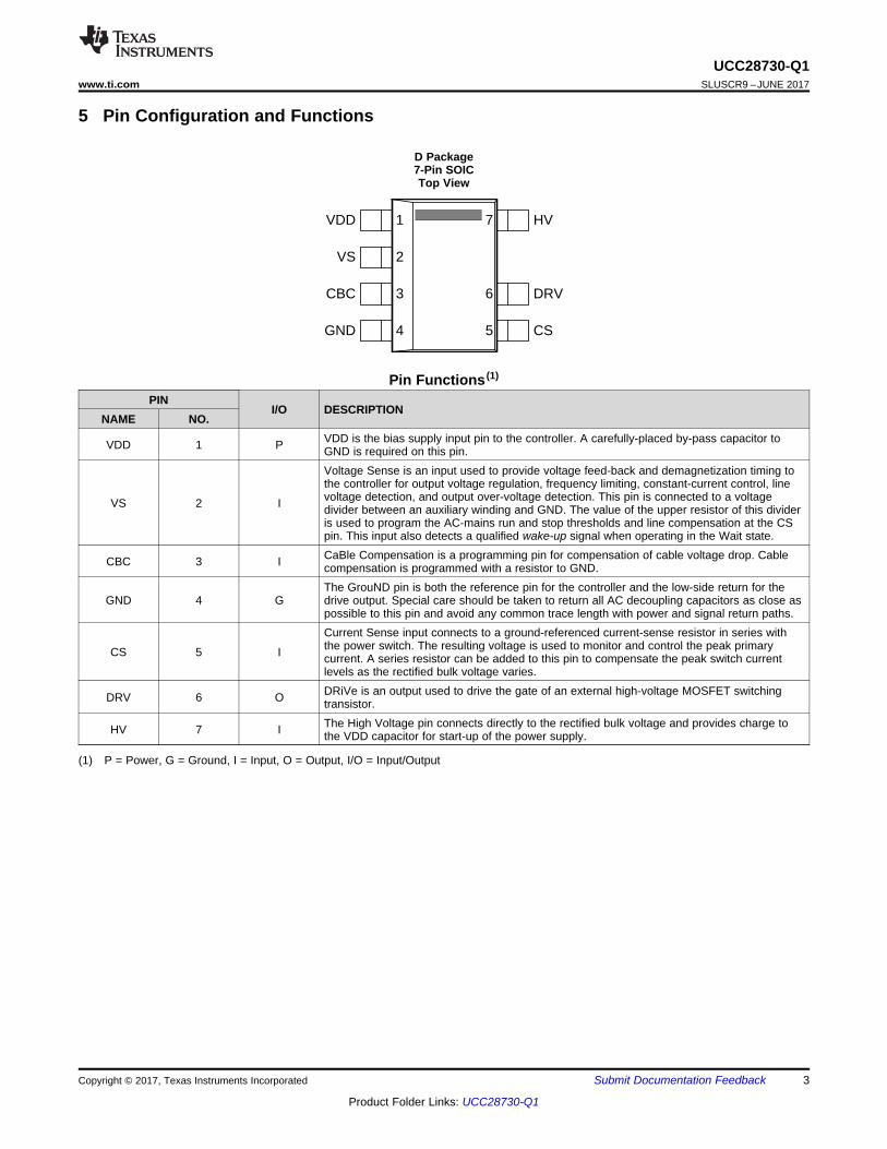


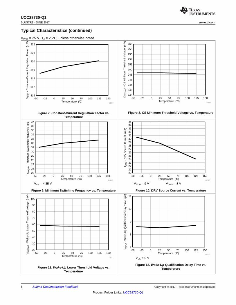


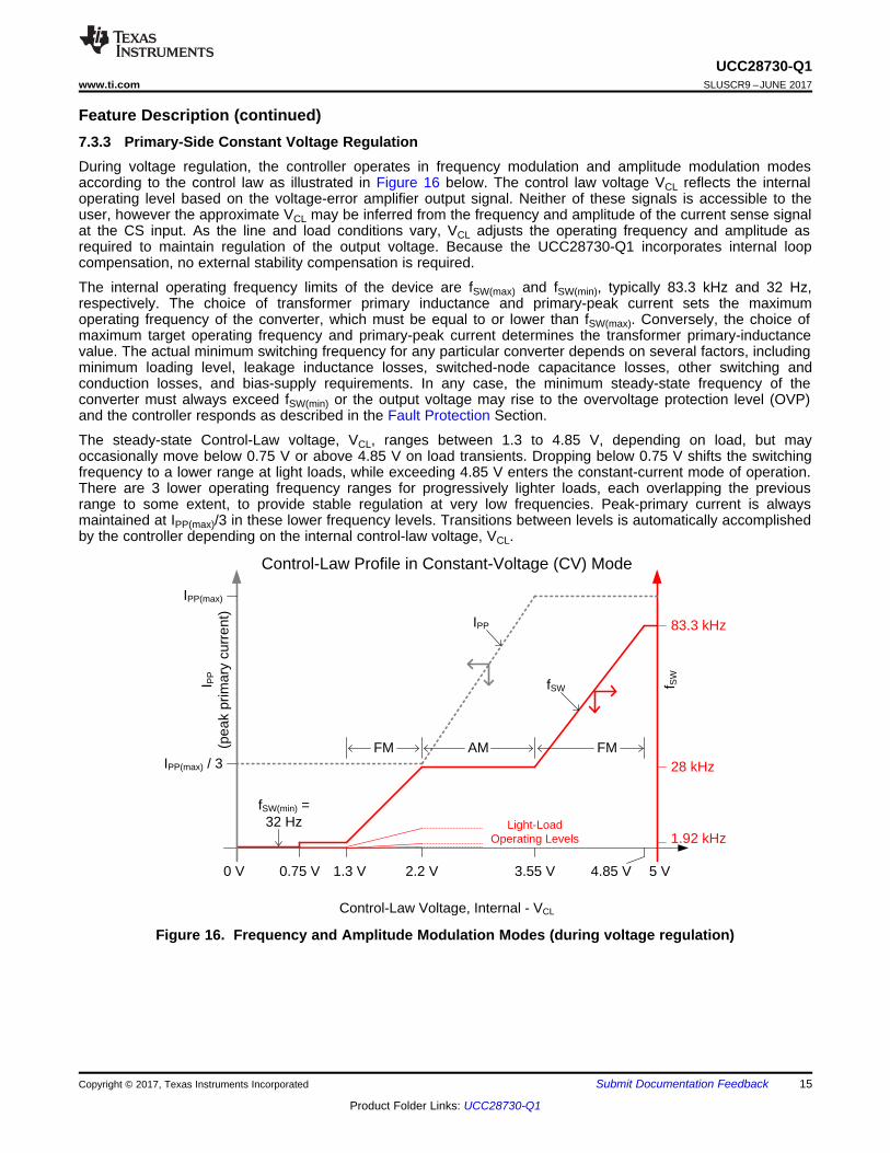

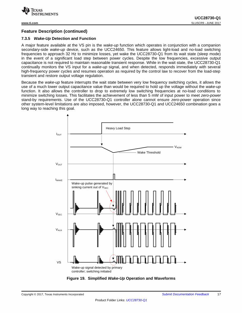

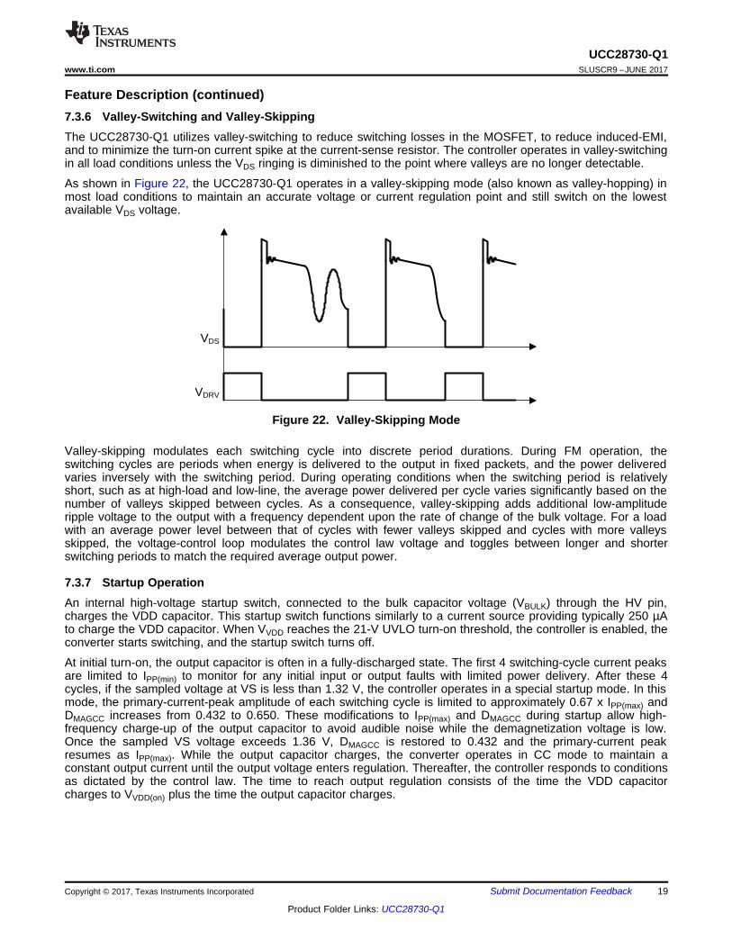


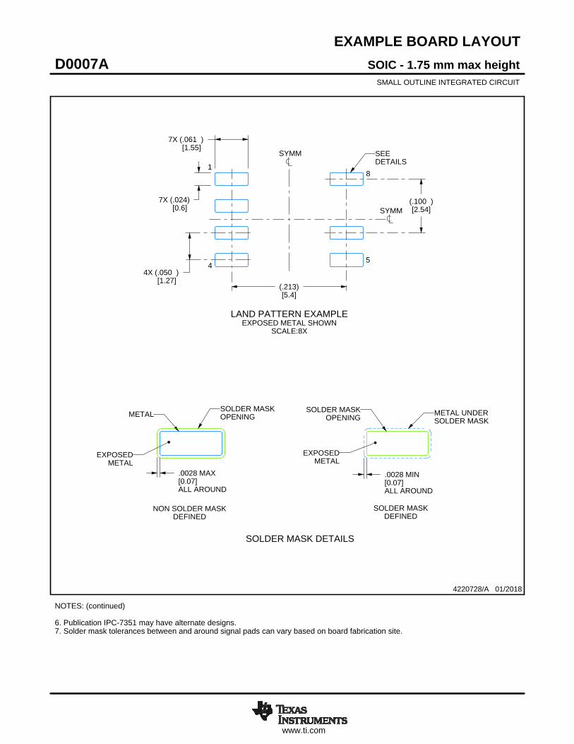


![SOURCE 300 VRMS PS-600-BS/300V PRELIMINARY USER MANUAL · Measuring range: 350 Vrms Accuracy: + / - 1.75 V [ELEC_160] Mains The power supply must be connected to the phase AC 230](https://static.documents.pub/doc/80x56/5e610c012ea18b1e715c6c56/source-300-vrms-ps-600-bs300v-preliminary-user-manual-measuring-range-350-vrms.jpg)


