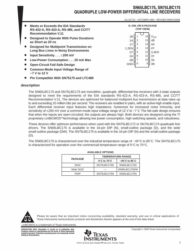
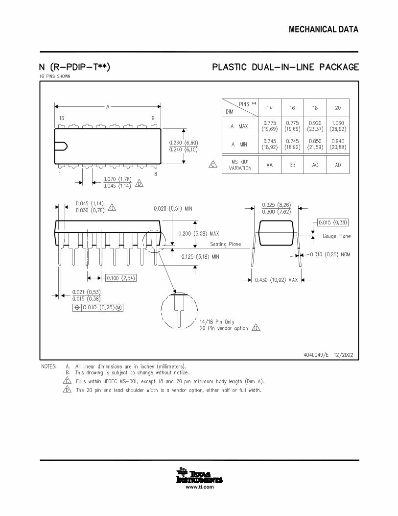
SN65LBC175, SN75LBC175 QUADRUPLE LOWĆPOWER DIFFERENTIAL LINE RECEIVERS SLLS171G - OCTOBER 1993 - REVISED MARCH2009 1 POST OFFICE BOX 655303 • DALLAS, TEXAS 75265 D Meets or Exceeds the EIA Standards RS-422-A, RS-423-A, RS-485, and CCITT Recommendation V.11 D Designed to Operate With Pulse Durations as Short as 20 ns D Designed for Multipoint Transmission on Long Bus Lines in Noisy Environments D Input Sensitivity . . . ± 200 mV D Low-Power Consumption . . . 20 mA Max D Open-Circuit Fail-Safe Design D Common-Mode Input Voltage Range of -7 V to 12 V D Pin Compatible With SN75175 and LTC489 description The SN65LBC175 and SN75LBC175 are monolithic, quadruple, differential line receivers with 3-state outputs designed to meet the requirements of the EIA standards RS-422-A, RS-423-A, RS-485, and CCITT Recommendation V.11. The devices are optimized for balanced multipoint bus transmission at data rates up to and exceeding 10 million bits per second. The receivers are enabled in pairs, with an active-high enable input. Each differential receiver input features high impedance, hysteresis for increased noise immunity, and sensitivity of ± 200 mV over a common-mode input voltage range of 12 V to -7 V. The fail-safe design ensures that when the inputs are open-circuited, the outputs are always high. Both devices are designed using the TI proprietary LinBiCMOStechnology allowing low power consumption, high switching speeds, and robustness. These devices offer optimum performance when used with the SN75LBC172 or SN75LBC174 quadruple line drivers. The SN65LBC175 is available in the 16-pin DIP (N), small-outline package (D), and the wide small-outline package (DW). The SN75LBC175 is available in the 16-pin DIP (N) and the small-outline package (D). The SN65LBC175 is characterized over the industrial temperature range of - 40°C to 85°C. The SN75LBC175 is characterized for operation over the commercial temperature range of 0°C to 70°C. AVAILABLE OPTIONS PACKAGE TEMPERATURE RANGE PACKAGE 0°C to 70°C -40°C to 85°C SOIC SN75LBC175D SN65LBC175D Wide SOIC SN65LBC175DW PDIP SN75LBC175N SN65LBC175N Please be aware that an important notice concerning availability, standard warranty, and use in critical applications of Texas Instruments semiconductor products and disclaimers thereto appears at the end of this data sheet. Copyright 2009 Texas Instruments Incorporated PRODUCTION DATA information is current as of publication date. Products conform to specifications per the terms of Texas Instruments standard warranty. Production processing does not necessarily include testing of all parameters. 1 2 3 4 5 6 7 8 16 15 14 13 12 11 10 9 1B 1A 1Y 1,2EN 2Y 2A 2B GND V CC 4B 4A 4Y 3,4EN 3Y 3A 3B D, DW, OR N PACKAGE (TOP VIEW) LinBiCMOS is a trademark of Texas Instruments.
Transcript
SLLS171G − OCTOBER 1993 − REVISED MARCH2009
1POST OFFICE BOX 655303 • DALLAS, TEXAS 75265
Meets or Exceeds the EIA StandardsRS-422-A, RS-423-A, RS-485, and CCITTRecommendation V.11
Designed to Operate With Pulse Durationsas Short as 20 ns
Designed for Multipoint Transmission onLong Bus Lines in Noisy Environments
Input Sensitivity . . . ±200 mV
Low-Power Consumptio n . . . 20 mA Max
Open-Circuit Fail-Safe Design
Common-Mode Input Voltage Range of−7 V to 12 V
Pin Compatible With SN75175 and LTC489
description
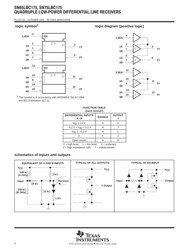
The SN65LBC175 and SN75LBC175 are monolithic, quadruple, differential line receivers with 3-state outputsdesigned to meet the requirements of the EIA standards RS-422-A, RS-423-A, RS-485, and CCITTRecommendation V.11. The devices are optimized for balanced multipoint bus transmission at data rates upto and exceeding 10 million bits per second. The receivers are enabled in pairs, with an active-high enable input.Each differential receiver input features high impedance, hysteresis for increased noise immunity, andsensitivity of ±200 mV over a common-mode input voltage range of 12 V to −7 V. The fail-safe design ensuresthat when the inputs are open-circuited, the outputs are always high. Both devices are designed using the TIproprietary LinBiCMOStechnology allowing low power consumption, high switching speeds, and robustness.
These devices offer optimum performance when used with the SN75LBC172 or SN75LBC174 quadruple linedrivers. The SN65LBC175 is available in the 16-pin DIP (N), small-outline package (D), and the widesmall-outline package (DW). The SN75LBC175 is available in the 16-pin DIP (N) and the small-outline package(D).
The SN65LBC175 is characterized over the industrial temperature range of −40°C to 85°C. The SN75LBC175is characterized for operation over the commercial temperature range of 0°C to 70°C.
AVAILABLE OPTIONS
PACKAGETEMPERATURE RANGE
PACKAGE0°C to 70°C −40°C to 85°C
SOIC SN75LBC175D SN65LBC175D
Wide SOIC SN65LBC175DW
PDIP SN75LBC175N SN65LBC175N
Please be aware that an important notice concerning availability, standard warranty, and use in critical applications ofTexas Instruments semiconductor products and disclaimers thereto appears at the end of this data sheet.
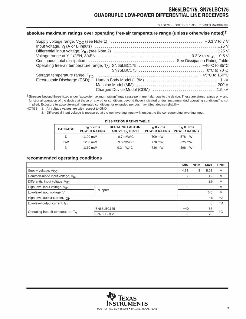
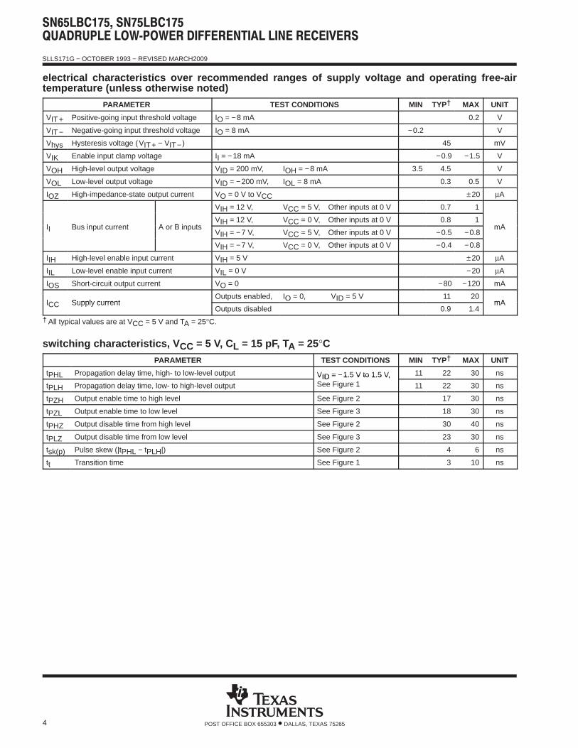
† Stresses beyond those listed under “absolute maximum ratings” may cause permanent damage to the device. These are stress ratings only, andfunctional operation of the device at these or any other conditions beyond those indicated under “recommended operating conditions” is notimplied. Exposure to absolute-maximum-rated conditions for extended periods may affect device reliability.
NOTES: 1. All voltage values are with respect to GND.2. Differential input voltage is measured at the noninverting input with respect to the corresponding inverting input.
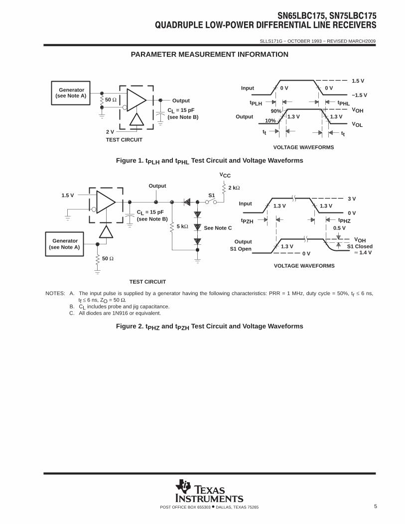
Figure 1. t PLH and t PHL Test Circuit and Voltage Waveforms
0 VS1 Open S1 Closed
1.3 V1.3 V
tPHZtPZH0.5 VSee Note C
VCC
2 kΩS1
5 kΩ
1.5 V
CL = 15 pF(see Note B)
Output
Generator(see Note A) 1.3 V
Input
Output
3 V
0 V
VOH
≈ 1.4 V50 Ω
TEST CIRCUIT
VOLTAGE WAVEFORMS
NOTES: A. The input pulse is supplied by a generator having the following characteristics: PRR = 1 MHz, duty cycle = 50%, tr ≤ 6 ns,tf ≤ 6 ns, ZO = 50 Ω.
B. CL includes probe and jig capacitance.C. All diodes are 1N916 or equivalent.
Figure 2. t PHZ and t PZH Test Circuit and Voltage Waveforms
SLLS171G − OCTOBER 1993 − REVISED MARCH2009
6 POST OFFICE BOX 655303 • DALLAS, TEXAS 75265
PARAMETER MEASUREMENT INFORMATION
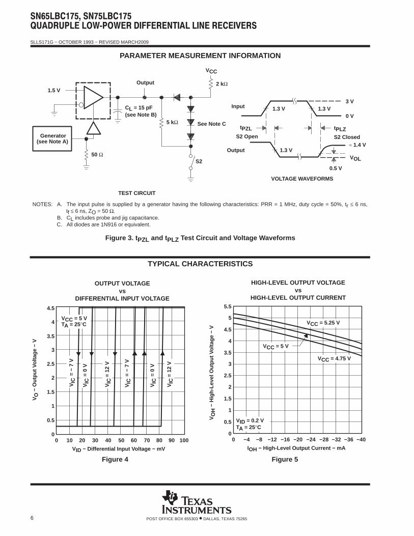
S2
0 V
3 V
S2 Closed
tPLZS2 Open
tPZL
VOL
Output
Input
1.3 V
(see Note A)Generator
Output
(see Note B)CL = 15 pF
1.5 V
See Note C
0.5 V
1.3 V 1.3 V
50 Ω
5 kΩ
2 kΩ
VCC
≈ 1.4 V
TEST CIRCUIT
VOLTAGE WAVEFORMS
NOTES: A. The input pulse is supplied by a generator having the following characteristics: PRR = 1 MHz, duty cycle = 50%, tr ≤ 6 ns,tf ≤ 6 ns, ZO = 50 Ω.
B. CL includes probe and jig capacitance.C. All diodes are 1N916 or equivalent.
Figure 3. t PZL and t PLZ Test Circuit and Voltage Waveforms
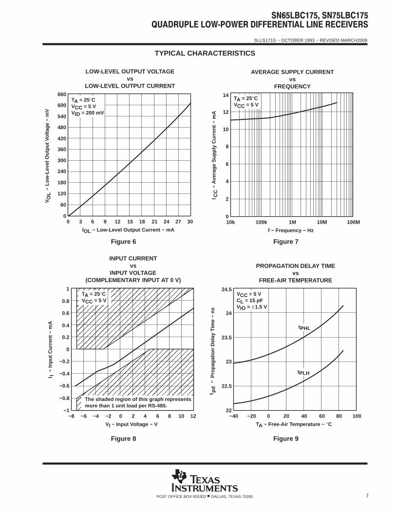
The shaded region of this graph representsmore than 1 unit load per RS-485.
Figure 9
23.5
23
22.5
22−40 −20 0 20 40 60
Pro
paga
tion
Del
ay T
ime
− ns 24
24.5
PROPAGATION DELAY TIMEvs
FREE-AIR TEMPERATURE
80 100
TA − Free-Air Temperature − °C
tPHL
tPLH
VCC = 5 VCL = 15 pFVIO = ±1.5 V
t pd
−
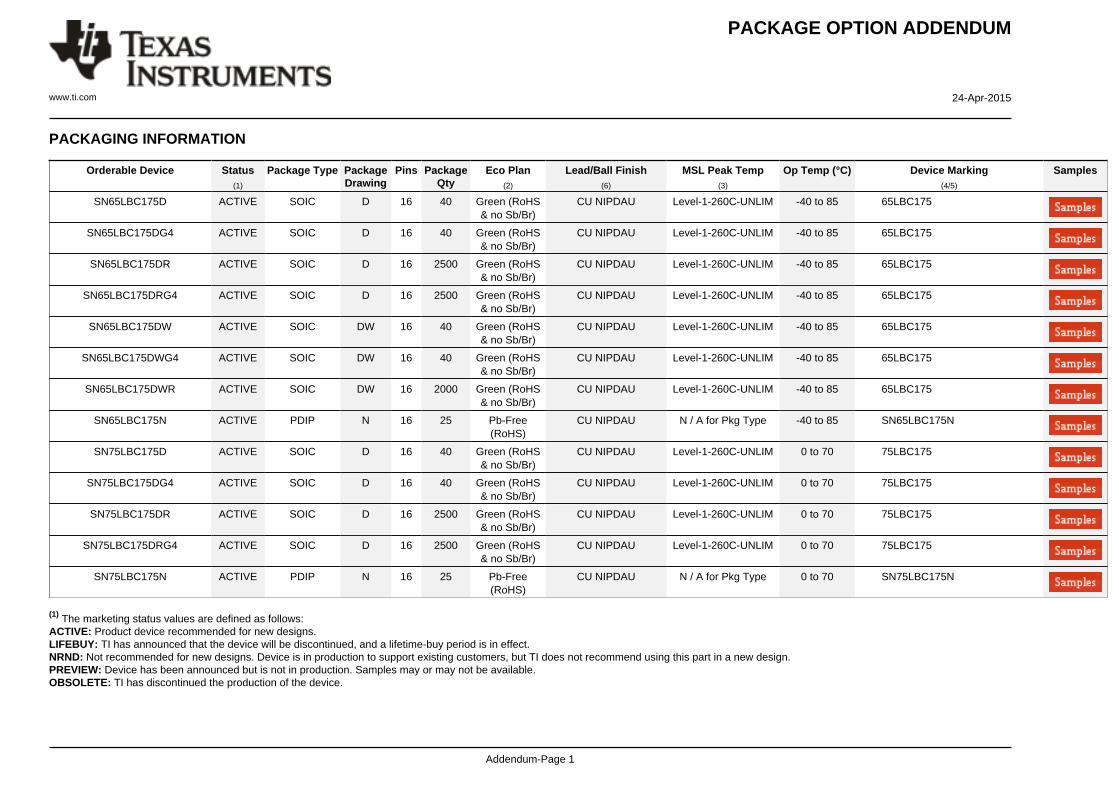
PACKAGE OPTION ADDENDUM
www.ti.com 24-Apr-2015
Addendum-Page 1
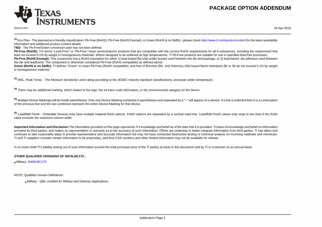
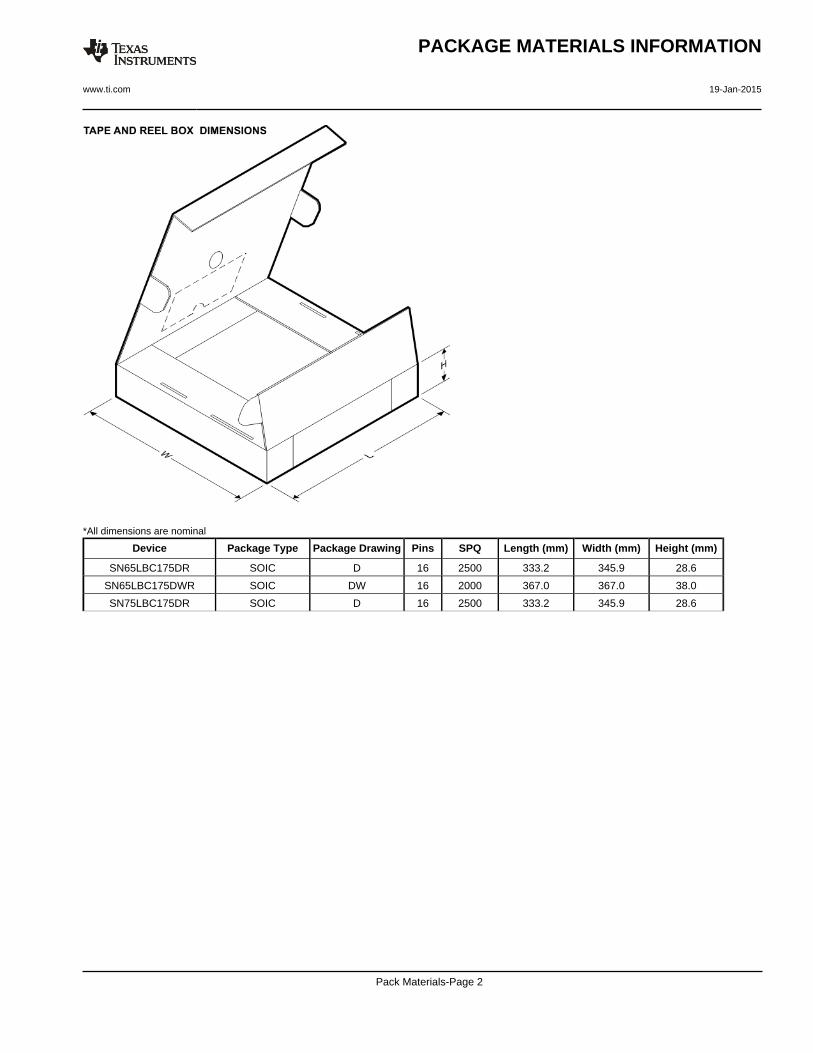
PACKAGING INFORMATION
Orderable Device Status(1)
Package Type PackageDrawing
Pins PackageQty
Eco Plan(2)
Lead/Ball Finish(6)
MSL Peak Temp(3)
Op Temp (°C) Device Marking(4/5)
Samples
SN65LBC175D ACTIVE SOIC D 16 40 Green (RoHS& no Sb/Br)
CU NIPDAU Level-1-260C-UNLIM -40 to 85 65LBC175
SN65LBC175DG4 ACTIVE SOIC D 16 40 Green (RoHS& no Sb/Br)
CU NIPDAU Level-1-260C-UNLIM -40 to 85 65LBC175
SN65LBC175DR ACTIVE SOIC D 16 2500 Green (RoHS& no Sb/Br)
CU NIPDAU Level-1-260C-UNLIM -40 to 85 65LBC175
SN65LBC175DRG4 ACTIVE SOIC D 16 2500 Green (RoHS& no Sb/Br)
CU NIPDAU Level-1-260C-UNLIM -40 to 85 65LBC175
SN65LBC175DW ACTIVE SOIC DW 16 40 Green (RoHS& no Sb/Br)
CU NIPDAU Level-1-260C-UNLIM -40 to 85 65LBC175
SN65LBC175DWG4 ACTIVE SOIC DW 16 40 Green (RoHS& no Sb/Br)
CU NIPDAU Level-1-260C-UNLIM -40 to 85 65LBC175
SN65LBC175DWR ACTIVE SOIC DW 16 2000 Green (RoHS& no Sb/Br)
CU NIPDAU Level-1-260C-UNLIM -40 to 85 65LBC175
SN65LBC175N ACTIVE PDIP N 16 25 Pb-Free(RoHS)
CU NIPDAU N / A for Pkg Type -40 to 85 SN65LBC175N
SN75LBC175D ACTIVE SOIC D 16 40 Green (RoHS& no Sb/Br)
CU NIPDAU Level-1-260C-UNLIM 0 to 70 75LBC175
SN75LBC175DG4 ACTIVE SOIC D 16 40 Green (RoHS& no Sb/Br)
CU NIPDAU Level-1-260C-UNLIM 0 to 70 75LBC175
SN75LBC175DR ACTIVE SOIC D 16 2500 Green (RoHS& no Sb/Br)
CU NIPDAU Level-1-260C-UNLIM 0 to 70 75LBC175
SN75LBC175DRG4 ACTIVE SOIC D 16 2500 Green (RoHS& no Sb/Br)
CU NIPDAU Level-1-260C-UNLIM 0 to 70 75LBC175
SN75LBC175N ACTIVE PDIP N 16 25 Pb-Free(RoHS)
CU NIPDAU N / A for Pkg Type 0 to 70 SN75LBC175N
(1) The marketing status values are defined as follows:ACTIVE: Product device recommended for new designs.LIFEBUY: TI has announced that the device will be discontinued, and a lifetime-buy period is in effect.NRND: Not recommended for new designs. Device is in production to support existing customers, but TI does not recommend using this part in a new design.PREVIEW: Device has been announced but is not in production. Samples may or may not be available.OBSOLETE: TI has discontinued the production of the device.
(2) Eco Plan - The planned eco-friendly classification: Pb-Free (RoHS), Pb-Free (RoHS Exempt), or Green (RoHS & no Sb/Br) - please check http://www.ti.com/productcontent for the latest availabilityinformation and additional product content details.TBD: The Pb-Free/Green conversion plan has not been defined.Pb-Free (RoHS): TI's terms "Lead-Free" or "Pb-Free" mean semiconductor products that are compatible with the current RoHS requirements for all 6 substances, including the requirement thatlead not exceed 0.1% by weight in homogeneous materials. Where designed to be soldered at high temperatures, TI Pb-Free products are suitable for use in specified lead-free processes.Pb-Free (RoHS Exempt): This component has a RoHS exemption for either 1) lead-based flip-chip solder bumps used between the die and package, or 2) lead-based die adhesive used betweenthe die and leadframe. The component is otherwise considered Pb-Free (RoHS compatible) as defined above.Green (RoHS & no Sb/Br): TI defines "Green" to mean Pb-Free (RoHS compatible), and free of Bromine (Br) and Antimony (Sb) based flame retardants (Br or Sb do not exceed 0.1% by weightin homogeneous material)
(3) MSL, Peak Temp. - The Moisture Sensitivity Level rating according to the JEDEC industry standard classifications, and peak solder temperature.
(4) There may be additional marking, which relates to the logo, the lot trace code information, or the environmental category on the device.
(5) Multiple Device Markings will be inside parentheses. Only one Device Marking contained in parentheses and separated by a "~" will appear on a device. If a line is indented then it is a continuationof the previous line and the two combined represent the entire Device Marking for that device.
(6) Lead/Ball Finish - Orderable Devices may have multiple material finish options. Finish options are separated by a vertical ruled line. Lead/Ball Finish values may wrap to two lines if the finishvalue exceeds the maximum column width.
Important Information and Disclaimer:The information provided on this page represents TI's knowledge and belief as of the date that it is provided. TI bases its knowledge and belief on informationprovided by third parties, and makes no representation or warranty as to the accuracy of such information. Efforts are underway to better integrate information from third parties. TI has taken andcontinues to take reasonable steps to provide representative and accurate information but may not have conducted destructive testing or chemical analysis on incoming materials and chemicals.TI and TI suppliers consider certain information to be proprietary, and thus CAS numbers and other limited information may not be available for release.
In no event shall TI's liability arising out of such information exceed the total purchase price of the TI part(s) at issue in this document sold by TI to Customer on an annual basis.
OTHER QUALIFIED VERSIONS OF SN75LBC175 :
• Military: SN55LBC175
NOTE: Qualified Version Definitions:
• Military - QML certified for Military and Defense Applications
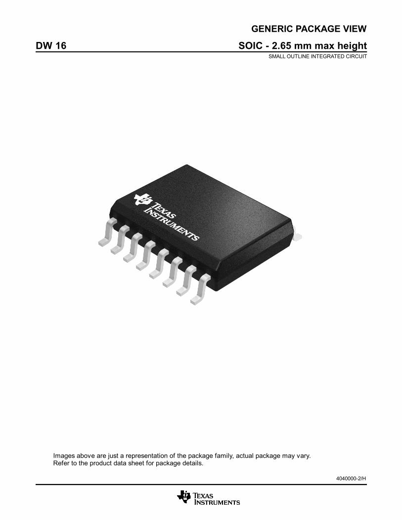
Images above are just a representation of the package family, actual package may vary.Refer to the product data sheet for package details.
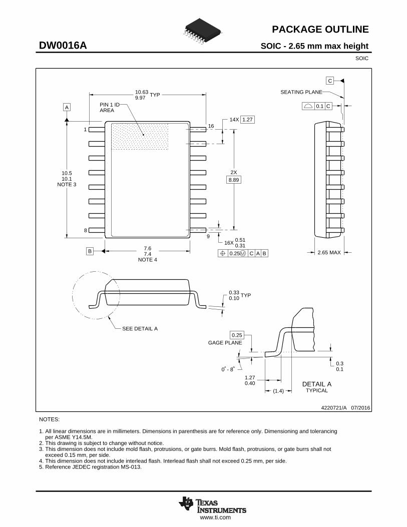
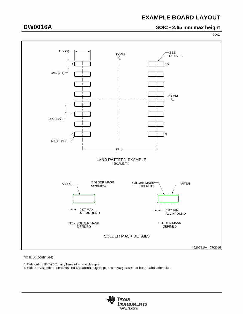
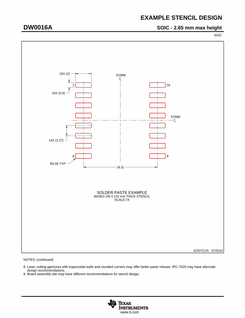
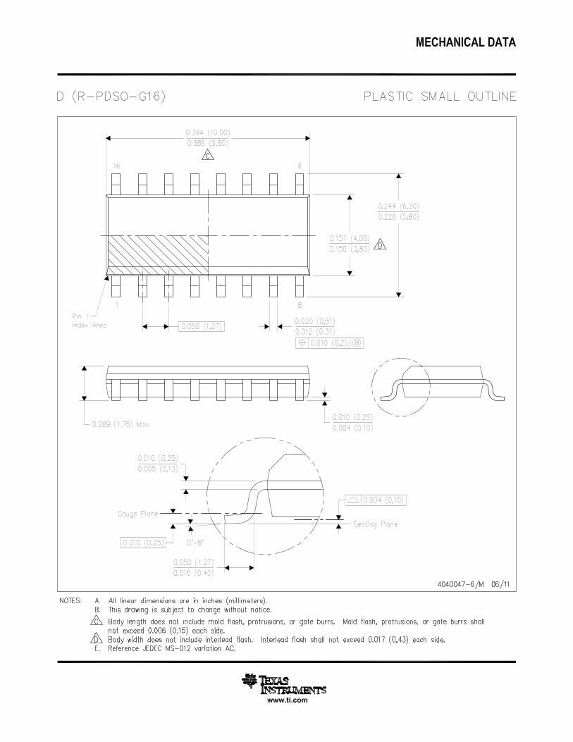
DW 16 SOIC - 2.65 mm max heightSMALL OUTLINE INTEGRATED CIRCUIT
4040000-2/H
www.ti.com
PACKAGE OUTLINE
C
TYP10.639.97
2.65 MAX
14X 1.27
16X 0.510.31
2X8.89
TYP0.330.10
0 - 80.30.1
(1.4)
0.25GAGE PLANE
1.270.40
A
NOTE 3
10.510.1
BNOTE 4
7.67.4
4220721/A 07/2016
SOIC - 2.65 mm max heightDW0016ASOIC
NOTES: 1. All linear dimensions are in millimeters. Dimensions in parenthesis are for reference only. Dimensioning and tolerancing per ASME Y14.5M. 2. This drawing is subject to change without notice. 3. This dimension does not include mold flash, protrusions, or gate burrs. Mold flash, protrusions, or gate burrs shall not exceed 0.15 mm, per side. 4. This dimension does not include interlead flash. Interlead flash shall not exceed 0.25 mm, per side.5. Reference JEDEC registration MS-013.
1 16
0.25 C A B
98
PIN 1 IDAREA
SEATING PLANE
0.1 C
SEE DETAIL A
DETAIL ATYPICAL
SCALE 1.500
www.ti.com
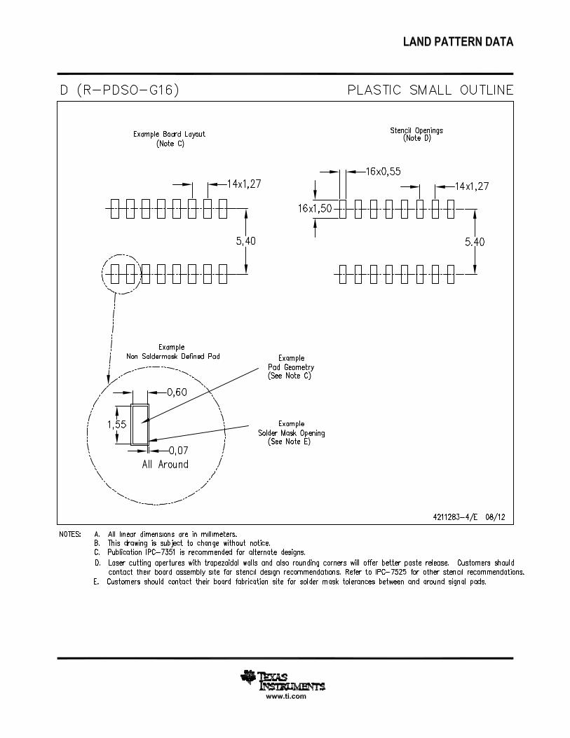
EXAMPLE BOARD LAYOUT
0.07 MAXALL AROUND
0.07 MINALL AROUND
(9.3)
14X (1.27)
R0.05 TYP
16X (2)
16X (0.6)
4220721/A 07/2016
SOIC - 2.65 mm max heightDW0016ASOIC
NOTES: (continued) 6. Publication IPC-7351 may have alternate designs. 7. Solder mask tolerances between and around signal pads can vary based on board fabrication site.
METAL SOLDER MASKOPENING
NON SOLDER MASKDEFINED
SOLDER MASK DETAILS
OPENINGSOLDER MASK METAL
SOLDER MASKDEFINED
LAND PATTERN EXAMPLESCALE:7X
SYMM
1
8 9
16
SEEDETAILS
SYMM
www.ti.com
EXAMPLE STENCIL DESIGN
R0.05 TYP
16X (2)
16X (0.6)
14X (1.27)
(9.3)
4220721/A 07/2016
SOIC - 2.65 mm max heightDW0016ASOIC
NOTES: (continued) 8. Laser cutting apertures with trapezoidal walls and rounded corners may offer better paste release. IPC-7525 may have alternate design recommendations. 9. Board assembly site may have different recommendations for stencil design.
SOLDER PASTE EXAMPLEBASED ON 0.125 mm THICK STENCIL
SCALE:7X
SYMM
SYMM
1
8 9
16
IMPORTANT NOTICE
Texas Instruments Incorporated (TI) reserves the right to make corrections, enhancements, improvements and other changes to itssemiconductor products and services per JESD46, latest issue, and to discontinue any product or service per JESD48, latest issue. Buyersshould obtain the latest relevant information before placing orders and should verify that such information is current and complete.TI’s published terms of sale for semiconductor products (http://www.ti.com/sc/docs/stdterms.htm) apply to the sale of packaged integratedcircuit products that TI has qualified and released to market. Additional terms may apply to the use or sale of other types of TI products andservices.Reproduction of significant portions of TI information in TI data sheets is permissible only if reproduction is without alteration and isaccompanied by all associated warranties, conditions, limitations, and notices. TI is not responsible or liable for such reproduceddocumentation. Information of third parties may be subject to additional restrictions. Resale of TI products or services with statementsdifferent from or beyond the parameters stated by TI for that product or service voids all express and any implied warranties for theassociated TI product or service and is an unfair and deceptive business practice. TI is not responsible or liable for any such statements.Buyers and others who are developing systems that incorporate TI products (collectively, “Designers”) understand and agree that Designersremain responsible for using their independent analysis, evaluation and judgment in designing their applications and that Designers havefull and exclusive responsibility to assure the safety of Designers' applications and compliance of their applications (and of all TI productsused in or for Designers’ applications) with all applicable regulations, laws and other applicable requirements. Designer represents that, withrespect to their applications, Designer has all the necessary expertise to create and implement safeguards that (1) anticipate dangerousconsequences of failures, (2) monitor failures and their consequences, and (3) lessen the likelihood of failures that might cause harm andtake appropriate actions. Designer agrees that prior to using or distributing any applications that include TI products, Designer willthoroughly test such applications and the functionality of such TI products as used in such applications.TI’s provision of technical, application or other design advice, quality characterization, reliability data or other services or information,including, but not limited to, reference designs and materials relating to evaluation modules, (collectively, “TI Resources”) are intended toassist designers who are developing applications that incorporate TI products; by downloading, accessing or using TI Resources in anyway, Designer (individually or, if Designer is acting on behalf of a company, Designer’s company) agrees to use any particular TI Resourcesolely for this purpose and subject to the terms of this Notice.TI’s provision of TI Resources does not expand or otherwise alter TI’s applicable published warranties or warranty disclaimers for TIproducts, and no additional obligations or liabilities arise from TI providing such TI Resources. TI reserves the right to make corrections,enhancements, improvements and other changes to its TI Resources. TI has not conducted any testing other than that specificallydescribed in the published documentation for a particular TI Resource.Designer is authorized to use, copy and modify any individual TI Resource only in connection with the development of applications thatinclude the TI product(s) identified in such TI Resource. NO OTHER LICENSE, EXPRESS OR IMPLIED, BY ESTOPPEL OR OTHERWISETO ANY OTHER TI INTELLECTUAL PROPERTY RIGHT, AND NO LICENSE TO ANY TECHNOLOGY OR INTELLECTUAL PROPERTYRIGHT OF TI OR ANY THIRD PARTY IS GRANTED HEREIN, including but not limited to any patent right, copyright, mask work right, orother intellectual property right relating to any combination, machine, or process in which TI products or services are used. Informationregarding or referencing third-party products or services does not constitute a license to use such products or services, or a warranty orendorsement thereof. Use of TI Resources may require a license from a third party under the patents or other intellectual property of thethird party, or a license from TI under the patents or other intellectual property of TI.TI RESOURCES ARE PROVIDED “AS IS” AND WITH ALL FAULTS. TI DISCLAIMS ALL OTHER WARRANTIES ORREPRESENTATIONS, EXPRESS OR IMPLIED, REGARDING RESOURCES OR USE THEREOF, INCLUDING BUT NOT LIMITED TOACCURACY OR COMPLETENESS, TITLE, ANY EPIDEMIC FAILURE WARRANTY AND ANY IMPLIED WARRANTIES OFMERCHANTABILITY, FITNESS FOR A PARTICULAR PURPOSE, AND NON-INFRINGEMENT OF ANY THIRD PARTY INTELLECTUALPROPERTY RIGHTS. TI SHALL NOT BE LIABLE FOR AND SHALL NOT DEFEND OR INDEMNIFY DESIGNER AGAINST ANY CLAIM,INCLUDING BUT NOT LIMITED TO ANY INFRINGEMENT CLAIM THAT RELATES TO OR IS BASED ON ANY COMBINATION OFPRODUCTS EVEN IF DESCRIBED IN TI RESOURCES OR OTHERWISE. IN NO EVENT SHALL TI BE LIABLE FOR ANY ACTUAL,DIRECT, SPECIAL, COLLATERAL, INDIRECT, PUNITIVE, INCIDENTAL, CONSEQUENTIAL OR EXEMPLARY DAMAGES INCONNECTION WITH OR ARISING OUT OF TI RESOURCES OR USE THEREOF, AND REGARDLESS OF WHETHER TI HAS BEENADVISED OF THE POSSIBILITY OF SUCH DAMAGES.Unless TI has explicitly designated an individual product as meeting the requirements of a particular industry standard (e.g., ISO/TS 16949and ISO 26262), TI is not responsible for any failure to meet such industry standard requirements.Where TI specifically promotes products as facilitating functional safety or as compliant with industry functional safety standards, suchproducts are intended to help enable customers to design and create their own applications that meet applicable functional safety standardsand requirements. Using products in an application does not by itself establish any safety features in the application. Designers mustensure compliance with safety-related requirements and standards applicable to their applications. Designer may not use any TI products inlife-critical medical equipment unless authorized officers of the parties have executed a special contract specifically governing such use.Life-critical medical equipment is medical equipment where failure of such equipment would cause serious bodily injury or death (e.g., lifesupport, pacemakers, defibrillators, heart pumps, neurostimulators, and implantables). Such equipment includes, without limitation, allmedical devices identified by the U.S. Food and Drug Administration as Class III devices and equivalent classifications outside the U.S.TI may expressly designate certain products as completing a particular qualification (e.g., Q100, Military Grade, or Enhanced Product).Designers agree that it has the necessary expertise to select the product with the appropriate qualification designation for their applicationsand that proper product selection is at Designers’ own risk. Designers are solely responsible for compliance with all legal and regulatoryrequirements in connection with such selection.Designer will fully indemnify TI and its representatives against any damages, costs, losses, and/or liabilities arising out of Designer’s non-compliance with the terms and provisions of this Notice.