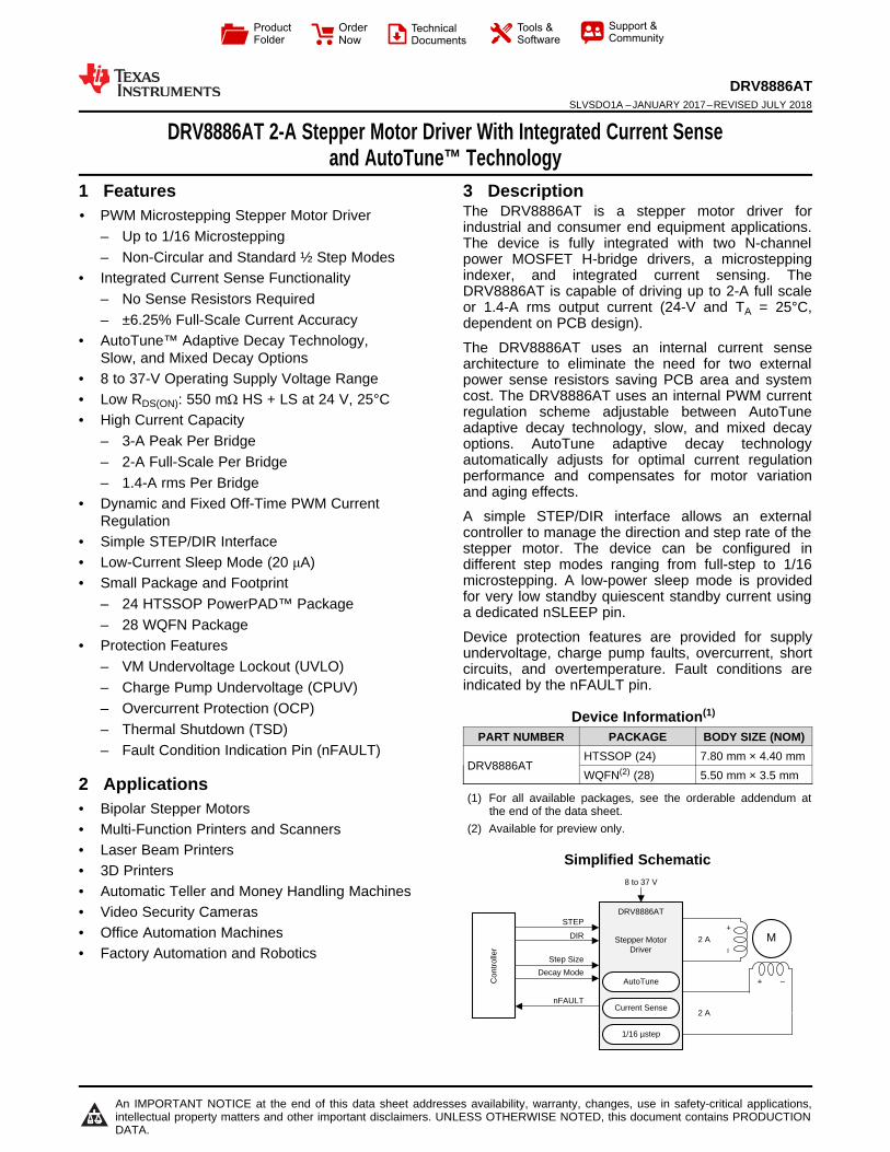
STEP Step Size Decay Mode 8 to 37 V Controller M + – + – DRV8886AT Current Sense 2 A 2 A 1/16 μstep DIR nFAULT AutoTune Stepper Motor Driver Product Folder Order Now Technical Documents Tools & Software Support & Community An IMPORTANT NOTICE at the end of this data sheet addresses availability, warranty, changes, use in safety-critical applications, intellectual property matters and other important disclaimers. UNLESS OTHERWISE NOTED, this document contains PRODUCTION DATA. DRV8886AT SLVSDO1A – JANUARY 2017 – REVISED JULY 2018 DRV8886AT 2-A Stepper Motor Driver With Integrated Current Sense and AutoTune™ Technology 1 1 Features 1• PWM Microstepping Stepper Motor Driver – Up to 1/16 Microstepping – Non-Circular and Standard ½ Step Modes • Integrated Current Sense Functionality – No Sense Resistors Required – ±6.25% Full-Scale Current Accuracy • AutoTune™ Adaptive Decay Technology, Slow, and Mixed Decay Options • 8 to 37-V Operating Supply Voltage Range • Low R DS(ON) : 550 mΩ HS + LS at 24 V, 25°C • High Current Capacity – 3-A Peak Per Bridge – 2-A Full-Scale Per Bridge – 1.4-A rms Per Bridge • Dynamic and Fixed Off-Time PWM Current Regulation • Simple STEP/DIR Interface • Low-Current Sleep Mode (20 μA) • Small Package and Footprint – 24 HTSSOP PowerPAD™ Package – 28 WQFN Package • Protection Features – VM Undervoltage Lockout (UVLO) – Charge Pump Undervoltage (CPUV) – Overcurrent Protection (OCP) – Thermal Shutdown (TSD) – Fault Condition Indication Pin (nFAULT) 2 Applications • Bipolar Stepper Motors • Multi-Function Printers and Scanners • Laser Beam Printers • 3D Printers • Automatic Teller and Money Handling Machines • Video Security Cameras • Office Automation Machines • Factory Automation and Robotics 3 Description The DRV8886AT is a stepper motor driver for industrial and consumer end equipment applications. The device is fully integrated with two N-channel power MOSFET H-bridge drivers, a microstepping indexer, and integrated current sensing. The DRV8886AT is capable of driving up to 2-A full scale or 1.4-A rms output current (24-V and T A = 25°C, dependent on PCB design). The DRV8886AT uses an internal current sense architecture to eliminate the need for two external power sense resistors saving PCB area and system cost. The DRV8886AT uses an internal PWM current regulation scheme adjustable between AutoTune adaptive decay technology, slow, and mixed decay options. AutoTune adaptive decay technology automatically adjusts for optimal current regulation performance and compensates for motor variation and aging effects. A simple STEP/DIR interface allows an external controller to manage the direction and step rate of the stepper motor. The device can be configured in different step modes ranging from full-step to 1/16 microstepping. A low-power sleep mode is provided for very low standby quiescent standby current using a dedicated nSLEEP pin. Device protection features are provided for supply undervoltage, charge pump faults, overcurrent, short circuits, and overtemperature. Fault conditions are indicated by the nFAULT pin. Device Information (1) PART NUMBER PACKAGE BODY SIZE (NOM) DRV8886AT HTSSOP (24) 7.80 mm × 4.40 mm WQFN (2) (28) 5.50 mm × 3.5 mm (1) For all available packages, see the orderable addendum at the end of the data sheet. (2) Available for preview only. Simplified Schematic
Transcript
STEP
Step Size
Decay Mode
8 to 37 V
Con
trol
ler
M
+ ±
+ ±
DRV8886AT
Current Sense
2 A
2 A
1/16 µstep
DIR
nFAULT
AutoTune
Stepper Motor Driver
Product
Folder
Order
Now
Technical
Documents
Tools &
Software
Support &Community
An IMPORTANT NOTICE at the end of this data sheet addresses availability, warranty, changes, use in safety-critical applications,intellectual property matters and other important disclaimers. UNLESS OTHERWISE NOTED, this document contains PRODUCTIONDATA.
DRV8886ATSLVSDO1A –JANUARY 2017–REVISED JULY 2018
DRV8886AT 2-A Stepper Motor Driver With Integrated Current Senseand AutoTune™ Technology
1
1 Features1• PWM Microstepping Stepper Motor Driver
– Up to 1/16 Microstepping– Non-Circular and Standard ½ Step Modes
• Integrated Current Sense Functionality– No Sense Resistors Required– ±6.25% Full-Scale Current Accuracy
• AutoTune™ Adaptive Decay Technology,Slow, and Mixed Decay Options
• 8 to 37-V Operating Supply Voltage Range• Low RDS(ON): 550 mΩ HS + LS at 24 V, 25°C• High Current Capacity
– 3-A Peak Per Bridge– 2-A Full-Scale Per Bridge– 1.4-A rms Per Bridge
• Dynamic and Fixed Off-Time PWM CurrentRegulation
• Simple STEP/DIR Interface• Low-Current Sleep Mode (20 μA)• Small Package and Footprint
2 Applications• Bipolar Stepper Motors• Multi-Function Printers and Scanners• Laser Beam Printers• 3D Printers• Automatic Teller and Money Handling Machines• Video Security Cameras• Office Automation Machines• Factory Automation and Robotics
3 DescriptionThe DRV8886AT is a stepper motor driver forindustrial and consumer end equipment applications.The device is fully integrated with two N-channelpower MOSFET H-bridge drivers, a microsteppingindexer, and integrated current sensing. TheDRV8886AT is capable of driving up to 2-A full scaleor 1.4-A rms output current (24-V and TA = 25°C,dependent on PCB design).
The DRV8886AT uses an internal current sensearchitecture to eliminate the need for two externalpower sense resistors saving PCB area and systemcost. The DRV8886AT uses an internal PWM currentregulation scheme adjustable between AutoTuneadaptive decay technology, slow, and mixed decayoptions. AutoTune adaptive decay technologyautomatically adjusts for optimal current regulationperformance and compensates for motor variationand aging effects.
A simple STEP/DIR interface allows an externalcontroller to manage the direction and step rate of thestepper motor. The device can be configured indifferent step modes ranging from full-step to 1/16microstepping. A low-power sleep mode is providedfor very low standby quiescent standby current usinga dedicated nSLEEP pin.
Device protection features are provided for supplyundervoltage, charge pump faults, overcurrent, shortcircuits, and overtemperature. Fault conditions areindicated by the nFAULT pin.
Device Information(1)
PART NUMBER PACKAGE BODY SIZE (NOM)
DRV8886ATHTSSOP (24) 7.80 mm × 4.40 mmWQFN(2) (28) 5.50 mm × 3.5 mm
(1) For all available packages, see the orderable addendum atthe end of the data sheet.
11 Device and Documentation Support ................. 3411.1 Documentation Support ........................................ 3411.2 Receiving Notification of Documentation Updates 3411.3 Community Resources.......................................... 3411.4 Trademarks ........................................................... 3411.5 Electrostatic Discharge Caution............................ 3411.6 Glossary ................................................................ 34
12 Mechanical, Packaging, and OrderableInformation ........................................................... 34
4 Revision HistoryNOTE: Page numbers for previous revisions may differ from page numbers in the current version.
Changes from Original (January 2017) to Revision A Page
• Added the WQFN package option ......................................................................................................................................... 1• Changed the units of the High-Side and Low-Side RDS(ON) axis labels from mΩ to Ω in the high-side and low-side
RDS(ON) over VM and over temperature graphs ...................................................................................................................... 9
STEP 19 20 I Step input. A rising edge causes the indexer to advance one step; internal pulldown resistor.
TRQ 23 24 I Current-scaling control. Scales the output current; tri-level pin.
VCP 3 1 PWR Charge pump output. Connect a X5R or X7R, 0.22-µF, 16-V ceramic capacitor to VM.
VM4 2
PWR Power supply. Connect to motor supply voltage and bypass to GND with two 0.01-µF ceramic capacitors (one foreach pin) plus a bulk capacitor rated for VM.11 9
nFAULT 15 16 OD Fault indication. Pulled logic low with fault condition; open-drain output requires an external pullup resistor.
nSLEEP 17 18 I Sleep mode input. Logic high to enable device; logic low to enter low-power sleep mode; internal pulldownresistor.
(1) Stresses beyond those listed under Absolute Maximum Ratings may cause permanent damage to the device. These are stress ratingsonly, which do not imply functional operation of the device at these or any other conditions beyond those indicated under RecommendedOperating Conditions. Exposure to absolute-maximum-rated conditions for extended periods may affect device reliability.
6 Specifications
6.1 Absolute Maximum Ratingsover operating free-air temperature range (unless otherwise noted) (1)
MIN MAX UNITPower supply voltage (VM) –0.3 40 VPower supply voltage ramp rate (VM) 0 2 V/µsCharge pump voltage (VCP, CPH) –0.3 VM + 7 VCharge pump negative switching pin (CPL) –0.3 VM VInternal regulator voltage (DVDD) –0.3 3.8 VInternal regulator current output (DVDD) 0 1 mAInternal regulator voltage (AVDD) –0.3 5.7 VControl pin voltage (STEP, DIR, ENABLE, nFAULT, M0, M1, DECAY, TRQ, nSLEEP) –0.3 5.7 VOpen drain output current (nFAULT) 0 10 mACurrent limit input pin voltage (RREF) –0.3 6.0 VContinuous phase node pin voltage (AOUT1, AOUT2, BOUT1, BOUT2) –1.0 VM + 1.0 VTransient 100 ns phase node pin voltage (AOUT1, AOUT2, BOUT1, BOUT2) –3.0 VM + 3.0 VPeak drive current (AOUT1, AOUT2, BOUT1, BOUT2) 0 3 AOperating junction temperature, TJ –40 150 °CStorage temperature, Tstg –65 150 °C
(1) JEDEC document JEP155 states that 500-V HBM allows safe manufacturing with a standard ESD control process.(2) JEDEC document JEP157 states that 250-V CDM allows safe manufacturing with a standard ESD control process.
6.2 ESD RatingsVALUE UNIT
V(ESD)Electrostaticdischarge
Human-body model (HBM), per ANSI/ESDA/JEDEC JS-001 (1) ±2000V
Charged-device model (CDM), per JEDEC specification JESD22-C101 (2) ±500
(1) STEP input can operate up to 500 kHz, but system bandwidth is limited by the motor load(2) Power dissipation and thermal limits must be observed
6.3 Recommended Operating Conditionsover operating free-air temperature range (unless otherwise noted)
MIN MAX UNITVVM Power supply voltage (VM) 8 37 V
VIInput voltage (DECAY, DIR, ENABLE, M0, M1, nSLEEP, STEP,TRQ) 0 5.3 V
ƒPWM Applied STEP signal (STEP) 0 100 (1) kHzIDVDD External load current (DVDD) 0 1 (2) mAIFS Motor full-scale current (xOUTx) 0 2 (2) AIrms Motor RMS current (xOUTx) 0 1.4 (2) ATA Operating ambient temperature –40 125 °C
(1) For more information about traditional and new thermal metrics, see the Semiconductor and IC Package Thermal Metrics applicationreport.
6.5 Electrical Characteristicsat TA = -40 to 125°C, VVM = 8 to 37 V (unless otherwise noted)
PARAMETER TEST CONDITIONS MIN TYP MAX UNITPOWER SUPPLIES (VM, DVDD, AVDD)VVM VM operating voltage 8 37 V
IVM VM operating supply current ENABLE = 1, nSLEEP = 1, No motorload 5 8 mA
IVMQ VM sleep mode supply currentnSLEEP = 0; TA = 25°C 20
μAnSLEEP = 0; TA = 125°C (1) 40
tSLEEP Sleep time nSLEEP = 0 to sleep-mode 50 200 μstWAKE Wake-up time nSLEEP = 1 to output transition 0.85 1.5 mstON Turn-on time VM > UVLO to output transition 0.85 1.5 msVDVDD Internal regulator voltage 0- to 1-mA external load 2.9 3.3 3.6 VVAVDD Internal regulator voltage No external load 4.5 5 5.5 VCHARGE PUMP (VCP, CPH, CPL)VVCP VCP operating voltage VM + 5.5 VLOGIC-LEVEL INPUTS (STEP, DIR, ENABLE, nSLEEP, M1)VIL Input logic-low voltage 0 0.8 VVIH Input logic-high voltage 1.6 5.3 VVHYS Input logic hysteresis 200 mVIIL Input logic-low current VIN = 0 V –1 1 μAIIH Input logic-high current VIN = 5 V 100 μARPD Pulldown resistance To GND 100 kΩtPD
(1) Propagation delay STEP to current change 1.2 μsTRI-LEVEL INPUT (M0, TRQ)VIL Tri-level input logic low voltage 0 0.65 VVIZ Tri-level input Hi-Z voltage 0.95 1.1 1.25 V
VIHTri-level input logic highvoltage 1.5 5.3 V
IIL Tri-level input logic low current VIN = 0 V –90 μA
IIHTri-level input logic highcurrent VIN = 5 V 155 μA
RPD Tri-level pulldown resistance VIN = Hi-Z, to GND 65 kΩRPU Tri-level pullup resistance VIN = Hi-Z, to DVDD 130 kΩQUAD-LEVEL INPUT (DECAY)VI1 Quad-level input voltage 1 Can set with 1% 5 kΩ to GND 0 0.14 VVI2 Quad-level input voltage 2 Can set with 1% 15 kΩ to GND 0.24 0.46 VVI3 Quad-level input voltage 3 Can set with 1% 44.2 kΩ to GND 0.71 1.24 VVI4 Quad-level input voltage 4 Can set with 1% 133 kΩ to GND 2.12 5.3 VIO Output current To GND 17 22 27.25 μACONTROL OUTPUTS (nFAULT)VOL Output logic-low voltage IO = 1 mA, RPULLUP = 4.7 kΩ 0.5 VIOH Output logic-high leakage VO = 5 V, RPULLUP = 4.7 kΩ –1 1 μA
Electrical Characteristics (continued)at TA = -40 to 125°C, VVM = 8 to 37 V (unless otherwise noted)
PARAMETER TEST CONDITIONS MIN TYP MAX UNITMOTOR DRIVER OUTPUTS (AOUT1, AOUT2, BOUT1, BOUT2)RDS(ON) High-side FET on resistance VM = 24 V, I = 1.4 A, TA = 25°C 290 346 mΩRDS(ON) Low-side FET on resistance VM = 24 V, I = 1.4 A, TA = 25°C 260 320 mΩtRISE
(1) Output rise time 100 nstFALL
(1) Output fall time 100 nstDEAD
(1) Output dead time 200 nsVd
(1) Body diode forward voltage IOUT = 0.5 A 0.7 1 VPWM CURRENT CONTROL (RREF)ARREF RREF transimpedance gain 28.1 30 31.9 kAΩVRREF RREF voltage RREF = 18 to 132 kΩ 1.18 1.232 1.28 VtOFF PWM off-time 20 μs
CRREFEquivalent capacitance onRREF 10 pF
tBLANK PWM blanking time
IRREF = 2.0 A, 63% to 100% currentsetting 1.5
µsIRREF = 2.0 A, 0% to 63% currentsetting 1
ΔITRIP Current trip accuracy
IRREF = 1.5 A, 10% to 20% currentsetting, 1% reference resistor –15% 15%
IRREF = 1.5 A, 20% to 63% currentsetting, 1% reference resistor –10% 10%
IRREF = 1.5 A, 71% to 100% currentsetting, 1% reference resistor –6.25% 6.25%
PROTECTION CIRCUITS
VUVLO VM UVLOVM falling, UVLO report 7 7.8
VVM rising, UVLO recovery 7.2 8
VUVLO,HYS Undervoltage hysteresis Rising to falling threshold 200 mVVCPUV Charge pump undervoltage VCP falling; CPUV report VM + 2 V
IOCPOvercurrent protection triplevel Current through any FET 3 A
tOCP(1) Overcurrent deglitch time 1.3 1.9 2.8 μs
tRETRY Overcurrent retry time 1 1.6 ms
TTSD(1) Thermal shutdown
temperature Die temperature TJ 150 °C
THYS(1) Thermal shutdown hysteresis Die temperature TJ 20 °C
(1) STEP input can operate up to 500 kHz, but system bandwidth is limited by the motor load.
6.6 Indexer Timing Requirementsat TA = -40 to 125°C, VVM = 8 to 37 V (unless otherwise noted)
NO. MIN MAX UNIT1 ƒSTEP
(1) Step frequency 500 kHz2 tWH(STEP) Pulse duration, STEP high 970 ns3 tWL(STEP) Pulse duration, STEP low 970 ns4 tSU(DIR, Mx) Setup time, DIR or USMx to STEP rising 200 ns5 tH(DIR, Mx) Hold time, DIR or USMx to STEP rising 200 ns
7.1 OverviewThe DRV8886AT device is an integrated motor-driver solution for bipolar stepper motors. The device integratestwo N-channel power MOSFET H-bridges, integrated current sense and regulation circuitry, and a microsteppingindexer. The DRV8886AT device can be powered with a supply voltage from 8 to 37 V and is capable ofproviding an output current up to 3-A peak, 2-A full-scale, or 1.4-A root mean square (rms). The actual full-scaleand rms current depends on the ambient temperature, supply voltage, and PCB thermal capability.
The DRV8886AT device uses an integrated current-sense architecture which eliminates the need for two externalpower sense resistors. This architecture removes the power dissipated in the sense resistors by using a currentmirror approach and using the internal power MOSFETs for current sensing. The current regulation set point isadjusted with a standard low-power resistor connected to the RREF pin. This features reduces externalcomponent cost, board PCB size, and system power consumption.
A simple STEP/DIR interface allows for an external controller to manage the direction and step rate of thestepper motor. The internal indexer can execute high-accuracy microstepping without requiring the externalcontroller to manage the winding current level. The indexer is capable of full step, half step, and 1/4, 1/8, 1/16microstepping. In addition to a standard half stepping mode, a noncircular half stepping mode is available forincreased torque output at higher motor RPM.
The current regulation is configurable between several decay modes. The decay mode can be selected as aslow-mixed, mixed decay, AutoTune Ripple Control, or AutoTune Dynamic Decay current regulation scheme.The slow-mixed decay mode uses slow decay on increasing steps and mixed decay on decreasing steps. TheAutoTune decay modes automatically adjust for optimal current regulation performance and compensate formotor variation and aging effects. AutoTune Ripple Control uses a variable off-time, ripple control scheme tominimize distortion of the motor winding current. AutoTune Dynamic Decay uses a fixed off-time, dynamic decaypercentage scheme to minimize distortion of the motor winding current while also minimizing frequency content.
An adaptive blanking time feature automatically scales the minimum drive time with output current level. Thisfeature helps alleviate zero-crossing distortion by limiting the drive time at low-current steps.
A torque DAC feature allows the controller to scale the output current without needing to scale the RREFreference resistor. The torque DAC is accessed using a digital input pin which allows the controller to savesystem power by decreasing the motor current consumption when high output torque is not required.
A low-power sleep mode is included which allows the system to save power when not actively driving the motor.
CVM1 VM GND Two X5R or X7R, 0.01-µF, VM-rated ceramic capacitorsCVM2 VM GND Bulk, VM-rated capacitorCVCP VCP VM X5R or X7R, 0.22-µF, 16-V ceramic capacitorCSW CPH CPL X5R or X7R, 0.022-µF, VM-rated ceramic capacitor
CAVDD AVDD GND X5R or X7R, 0.47-µF, 6.3-V ceramic capacitorCDVDD DVDD GND X5R or X7R, 0.47-µF, 6.3-V ceramic capacitor
RnFAULT VCC (1) nFAULT >4.7-kΩ resistor
RREF RREF GND Resistor to limit chopping current must be installed. See the Typical Applicationsection for value selection.
7.3.1 Stepper Motor Driver Current RatingsStepper motor drivers can be classified using three different numbers to describe the output current: peak, rms,and full-scale.
7.3.1.1 Peak Current RatingThe peak current in a stepper driver is limited by the overcurrent protection trip threshold IOCP. The peak currentdescribes any transient duration current pulse, for example when charging capacitance, when the overall dutycycle is very low. In general the minimum value of IOCP specifies the peak current rating of the stepper motordriver. For the DRV8886AT device, the peak current rating is 3 A per bridge.
7.3.1.2 rms Current RatingThe rms (average) current is determined by the thermal considerations of the IC. The rms current is calculatedbased on the RDS(ON), rise and fall time, PWM frequency, device quiescent current, and package thermalperformance in a typical system at 25°C. The actual operating rms current may be higher or lower depending onheatsinking and ambient temperature. For the DRV8886AT device, the rms current rating is 1.4 A per bridge.
7.3.1.3 Full-Scale Current RatingThe full-scale current describes the top of the sinusoid current waveform while microstepping. Because thesinusoid amplitude is related to the rms current, the full-scale current is also determined by the thermalconsiderations of the device. The full-scale current rating is approximately √2 × IRMS. The full-scale current is setby the RREF pin and the torque DAC when configuring the DRV8886AT device, for details see the CurrentRegulation section. For the DRV8886AT device, the full-scale current rating is 2 A per bridge.
7.3.2 PWM Motor DriversThe DRV8886AT device has drivers for two full H-bridges to drive the two windings of a bipolar stepper motor.Figure 13 shows a block diagram of the circuitry.
Figure 13. PWM Motor Driver Block Diagram
7.3.3 Microstepping IndexerBuilt-in indexer logic in the DRV8886AT device allows a number of different step modes. The M1 and M0 pinsare used to configure the step mode as shown in Table 2.
Table 2. Microstepping SettingsM1 M0 STEP MODE0 0 Full step (2-phase excitation) with 71% current0 1 1/16 step1 0 1/2 step1 1 1/4 step0 Z 1/8 step1 Z Non-circular 1/2 step
Table 3 shows the relative current and step directions for full-step through 1/16-step operation. The AOUTcurrent is the sine of the electrical angle and the BOUT current is the cosine of the electrical angle. Positivecurrent is defined as current flowing from the xOUT1 pin to the xOUT2 pin while driving.
At each rising edge of the STEP input the indexer travels to the next state in the table. The direction is shownwith the DIR pin logic high. If the DIR pin is logic low, the sequence is reversed.
On power-up or when exiting sleep mode, keep the STEP pin logic low, otherwise the indexer advances onestep.
NOTEIf the step mode is changed from full, 1/2, 1/4, 1/8, or 1/16 to full, 1/2, 1/4, 1/8, or 1/16while stepping, the indexer advances to the next valid state for the new step mode settingat the rising edge of STEP. If the step mode is changed from or to noncircular 1/2 step theindexer goes immediately to the valid state for that mode.
The home state is an electrical angle of 45°. This state is entered after power-up, after exiting logic undervoltagelockout, or after exiting sleep mode. Table 3 lists the home state in red.
Table 3. Microstepping Relative Current Per Step (DIR = 1)FULL STEP 1/2 STEP 1/4 STEP 1/8 STEP 1/16 STEP ELECTRICAL
Table 4 shows the noncircular 1/2–step operation. This stepping mode consumes more power than circular 1/2-step operation, but provides a higher torque at high motor RPM.
Table 4. Non-Circular 1/2-Stepping CurrentNON-CIRCULAR 1/2-STEP AOUT CURRENT
7.3.4 Current RegulationThe current through the motor windings is regulated by an adjustable, fixed-off-time PWM current-regulationcircuit. When an H-bridge is enabled, current rises through the winding at a rate dependent on the DC voltage,inductance of the winding, and the magnitude of the back EMF present. When the current hits the currentregulation threshold, the bridge enters a decay mode for a fixed 20 μs, period of time to decrease the current.After the off time expires, the bridge is re-enabled, starting another PWM cycle.
Figure 14. Current Chopping Waveform
The PWM regulation current is set by a comparator which monitors the voltage across the current senseMOSFETs in parallel with the low-side power MOSFETs. The current sense MOSFETs are biased with areference current that is the output of a current-mode sine-weighted DAC whose full-scale reference current isset by the current through the RREF pin. An external resistor is placed from the RREF pin to GND to set thereference current. In addition, the TRQ pin can further scale the reference current.
Use Equation 1 to calculate the full-scale regulation current.
(1)
For example, if a 30-kΩ resistor is connected to the RREF pin, the full-scale regulation current is 1 A (TRQ at100%).
The TRQ pin is the input to a DAC used to scale the output current. Table 5 lists the current scalar value fordifferent inputs.
Table 5. Torque DAC SettingsTRQ CURRENT SCALAR (TRQ)
7.3.5 Controlling RREF With an MCU DACIn some cases, the full-scale output current may need to be changed between many different values, dependingon motor speed and loading. The reference current of the RREF pin can be adjusted in the system by tying theRREF resistor to a DAC output instead of GND.
In this mode of operation, as the DAC voltage increases, the reference current decreases and therefore the full-scale regulation current decreases as well. For proper operation, the output of the DAC should not rise aboveVRREF.
Figure 15. Controlling RREF with a DAC Resource
Use Equation 2 to calculate the full-scale regulation current as controlled by a controller DAC.
(2)
For example, if a 20-kΩ resistor is connected from the RREF pin to the DAC, and the DAC outputs 0.74 V, thechopping current is 600 mA (TRQ at 100%)
The RREF pin can also be adjusted using a PWM signal and low-pass filter.
7.3.6 Decay ModesThe DRV8886AT decay mode is selected by setting the quad-level DECAY pin to the voltage range listed inTable 6. The decay mode setting is latched on device enable.
100 mVCan be tied to ground Slow decay Mixed decay: 30% fast
300 mV, 15 kΩ to GND Mixed decay: 30% fast Mixed decay: 30% fast1.0 V, 45 kΩ to GND AutoTune Ripple Control AutoTune Ripple Control2.9 VCan be tied to DVDD AutoTune Dynamic Decay AutoTune Dynamic Decay
Figure 17 defines increasing and decreasing current. For the slow-mixed decay mode, the decay mode is set asslow during increasing current steps and mixed decay during decreasing current steps. In full step mode thedecreasing steps decay mode is always used. In noncircular 1/2-step mode the increasing step decay mode isused after a level transition (0% to 100% and 0% to –100%). When the level transition is to a similar level (100%to 100% and –100% to –100%), the decreasing step decay mode is used.
Figure 17. Definition of Increasing and Decreasing Steps
7.3.6.1 Mode 1: Slow Decay for Increasing Current, Mixed Decay for Decreasing Current
Figure 18. Slow-Mixed Decay Mode
Mixed decay begins as fast decay for a time, followed by slow decay for the remainder of the tOFF time. In thismode, mixed decay only occurs during decreasing current. Slow decay is used for increasing current.
This mode exhibits the same current ripple as slow decay for increasing current, because for increasing current,only slow decay is used. For decreasing current, the ripple is larger than slow decay, but smaller than fast decay.On decreasing current steps, mixed decay settles to the new ITRIP level faster than slow decay.
7.3.6.2 Mode 2: Mixed Decay for Increasing and Decreasing Current
Figure 19. Mixed-Mixed Decay Mode
Mixed decay begins as fast decay for a time, followed by slow decay for the remainder of tOFF. In this mode,mixed decay occurs for both increasing and decreasing current steps.
This mode exhibits ripple larger than slow decay, but smaller than fast decay. On decreasing current steps,mixed decay settles to the new ITRIP level faster than slow decay.
In cases where current is held for a long time (no input in the STEP pin) or at very low stepping speeds, slowdecay may not properly regulate current because no back-EMF is present across the motor windings. In thisstate, motor current can rise very quickly, and requires an excessively large off-time. Increasing or decreasingmixed decay mode allows the current level to stay in regulation when no back-EMF is present across the motorwindings.
7.3.6.3 Mode 3: AutoTune Ripple ControlThe AutoTune current regulation schemes are advanced current-regulation control methods that use additionalcomponents as compared to traditional fixed off-time current regulation schemes. AutoTune current regulationschemes help the stepper motor driver adjust the decay scheme based on operating factors such as the oneslisted as follows:
• Motor winding resistance and inductance• Motor aging effects• Motor dynamic speed and load• Motor supply voltage variation• Motor back-EMF difference on rising and falling steps• Step transitions• Low-current versus high-current dI/dt
The DRV8886AT device provides two different AutoTune current regulation modes, named AutoTune RippleControl and AutoTune Dynamic Decay.
Figure 20. AutoTune Ripple Control Decay Mode
AutoTune Ripple Control operates by setting an IVALLEY level alongside the ITRIP level. When the current levelreaches ITRIP, instead of entering slow decay until the tOFF time expires, the driver enters slow decay until IVALLEYis reached. Slow decay operates similar to mode 1 in which both low-side MOSFETs are turned on allowing thecurrent to recirculate. In this mode, tOFF varies depending on the current level and operating conditions.
This method allows much tighter regulation of the current level increasing motor efficiency and systemperformance. AutoTune Ripple Control can be used in systems that can tolerate a variable off-time regulationscheme to achieve small current ripple in the current regulation.
AutoTune Dynamic Decay greatly simplifies the decay mode selection by automatically configuring the decaymode between slow, mixed, and fast decay. In mixed decay, AutoTune dynamically adjusts the fast decaypercentage of the total mixed decay time. This feature eliminates motor tuning by automatically determining thebest decay setting that results in the lowest ripple for the motor.
The decay mode setting is optimized iteratively each PWM cycle. If the motor current overshoots the target triplevel, then the decay mode becomes more aggressive (add fast decay percentage) on the next cycle to preventregulation loss. If a long drive time must occur to reach the target trip level, the decay mode becomes lessaggressive (remove fast decay percentage) on the next cycle to operate with less ripple and more efficiently. Onfalling steps, AutoTune Dynamic Decay automatically switches to fast decay to reach the next step quickly.
AutoTune Dynamic Decay is optimal for applications that require minimal current ripple but want to maintain afixed frequency in the current regulation scheme.
7.3.7 Blanking TimeAfter the current is enabled in an H-bridge, the current sense comparator is ignored for a period of time (tBLANK)before enabling the current-sense circuitry. The blanking time also sets the minimum drive time of the PWM.Table 7 shows the blanking time based on the sine table index and the torque DAC setting. In the AutoTunecurrent regulation modes the blanking time is fixed at 1.0 µs. Please note that the torque DAC index is not thesame as one step as given in Table 3.
Table 7. Adaptive BlankingTime over Torque DAC and
7.3.8 Charge PumpA charge pump is integrated to supply a high-side N-channel MOSFET gate-drive voltage. The charge pumprequires a capacitor between the VM and VCP pins to act as the storage capacitor. Additionally a ceramiccapacitor is required between the CPH and CPL pins to act as the flying capacitor.
7.3.9 Linear Voltage RegulatorsAn linear voltage regulator is integrated into the DRV8886AT device. The DVDD regulator can be used to providea reference voltage. For proper operation, bypass the DVDD pin to GND using a ceramic capacitor.
The DVDD output is nominally 3.3 V. When the DVDD LDO current load exceeds 1 mA, the output voltage dropssignificantly.
The AVDD pin also requires a bypass capacitor to GND. This LDO is for DRV8886AT internal use only.
Figure 23. Linear Voltage Regulator Block Diagram
If a digital input must be tied permanently high (that is, Mx, DECAY or TRQ), tying the input to the DVDD pininstead of an external regulator is preferred. This method saves power when the VM pin is not applied or in sleepmode: the DVDD regulator is disabled and current does not flow through the input pulldown resistors. Forreference, logic level inputs have a typical pulldown of 100 kΩ, and tri-level inputs have a typical pulldown of 60kΩ.
7.3.10 Logic and Multi-Level Pin DiagramsFigure 24 shows the input structure for the logic-level pins STEP, DIR, ENABLE, nSLEEP, and M1.
Figure 24. Logic-Level Input Pin Diagram
The tri-level logic pins, M0 and TRQ, have the structure shown in Figure 25.
The quad-level logic pin, DECAY, has the structure shown in Figure 26.
Figure 26. Quad-Level Input Pin Diagram
7.3.11 Protection CircuitsThe DRV8886AT device is fully protected against supply undervoltage, charge pump undervoltage, outputovercurrent, and device overtemperature events.
7.3.11.1 VM Undervoltage Lockout (UVLO)If at any time the voltage on the VM pin falls below the VM undervoltage-lockout threshold voltage (VUVLO), allMOSFETs in the H-bridge are disabled, the charge pump is disabled, the logic is reset, and the nFAULT pin isdriven low. Operation resumes when the VM voltage rises above the VUVLO threshold. The nFAULT pin isreleased after operation resumes. Decreasing the VM voltage below this undervoltage threshold resets theindexer position.
7.3.11.2 VCP Undervoltage Lockout (CPUV)If at any time the voltage on the VCP pin falls below the charge-pump undervoltage-lockout threshold voltage(VCPUV), all MOSFETs in the H-bridge are disabled and the nFAULT pin is driven low. Operation resumes whenthe VCP voltage rises above the VCPUV threshold. The nFAULT pin is released after operation resumes.
7.3.11.3 Overcurrent Protection (OCP)An analog current limit circuit on each MOSFET limits the current through the MOSFET by removing the gatedrive. If this analog current limit persists for longer than tOCP, all MOSFETs in the H-bridge are disabled and thenFAULT pin is driven low.
The driver is re-enabled after the OCP retry period (tRETRY) has passed. The nFAULT pin becomes high again atafter the retry time. If the fault condition is still present, the cycle repeats. If the fault is no longer present, normaloperation resumes and nFAULT remains deasserted.
7.3.11.4 Thermal Shutdown (TSD)If the die temperature exceeds the TTSD level, all MOSFETs in the H-bridge are disabled and the nFAULT pin isdriven low. When the die temperature falls below the TTSD level, operation automatically resumes. The nFAULTpin is released after operation resumes.
7.4 Device Functional ModesThe DRV8886AT device is active unless the nSLEEP pin is brought logic low. In sleep mode the charge pump isdisabled, the H-bridge FETs are disabled Hi-Z, and the regulators are disabled.
NOTEThe tSLEEP time must elapse after a falling edge on the nSLEEP pin before the device is insleep mode. The DRV8886AT device is brought out of sleep mode automatically ifnSLEEP is brought logic high.
The tWAKE time must elapse before the outputs change state after wake-up.
TI recommends to keep the STEP pin logic low when coming out of nSLEEP or when applying power.
If the ENABLE pin is brought logic low, the H-bridge outputs are disabled, but the internal logic is still active. Arising edge on STEP advances the indexer, but the outputs do not change state until the ENABLE pin isasserted.
NOTEInformation in the following applications sections is not part of the TI componentspecification, and TI does not warrant its accuracy or completeness. TI’s customers areresponsible for determining suitability of components for their purposes. Customers shouldvalidate and test their design implementation to confirm system functionality.
8.1 Application InformationThe DRV8886AT device is used in bipolar stepper control.
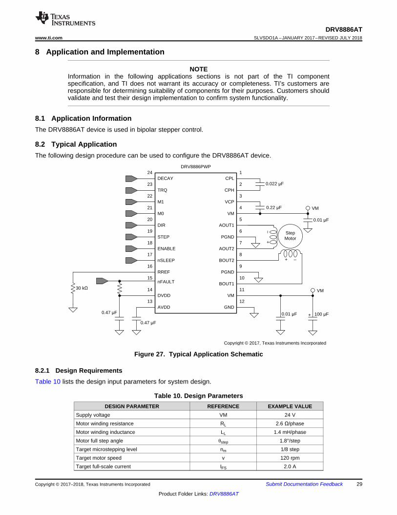
8.2 Typical ApplicationThe following design procedure can be used to configure the DRV8886AT device.
Figure 27. Typical Application Schematic
8.2.1 Design RequirementsTable 10 lists the design input parameters for system design.
Table 10. Design ParametersDESIGN PARAMETER REFERENCE EXAMPLE VALUE
Supply voltage VM 24 VMotor winding resistance RL 2.6 Ω/phaseMotor winding inductance LL 1.4 mH/phaseMotor full step angle θstep 1.8°/stepTarget microstepping level nm 1/8 stepTarget motor speed v 120 rpmTarget full-scale current IFS 2.0 A
8.2.2.1 Stepper Motor SpeedThe first step in configuring the DRV8886AT device requires the desired motor speed and microstepping level. Ifthe target application requires a constant speed, then a square wave with frequency ƒstep must be applied to theSTEP pin.
If the target motor speed is too high, the motor does not spin. Make sure that the motor can support the targetspeed.
Use Equation 3 to calculate ƒstep for a desired motor speed (v), microstepping level (nm), and motor full stepangle (θstep)
(3)
The value of θstep can be found in the stepper motor data sheet, or written on the motor.
For the DRV8886AT device, the microstepping level is set by the Mx pins and can be any of the settings listed inTable 11. Higher microstepping results in a smoother motor motion and less audible noise, but increasesswitching losses and requires a higher ƒstep to achieve the same motor speed.
Table 11. Microstepping Indexer SettingsM1 M0 STEP MODE0 0 Full step (2-phase excitation) with 71% current0 1 1/16 step1 0 1/2 step1 1 1/4 step0 Z 1/8 step1 Z Non-circular 1/2 step
For example, the motor is 1.8°/step for a target of 120 rpm at 1/8 microstep mode.
(4)
8.2.2.2 Current RegulationIn a stepper motor, the full-scale current (IFS) is the maximum current driven through either winding. This quantitydepends on the RREF resistor and the TRQ setting. During stepping, IFS defines the current chopping threshold(ITRIP) for the maximum current step.
(5)
NOTEThe IFS current must also follow Equation 6 to avoid saturating the motor. VM is the motorsupply voltage, and RL is the motor winding resistance.
(6)
8.2.2.3 Decay ModesThe DRV8886AT device supports three different decay modes: slow decay, slow-mixed and all mixed decay. Thecurrent through the motor windings is regulated using an adjustable fixed-time-off scheme which means that afterany drive phase, when a motor winding current has hit the current chopping threshold (ITRIP), the DRV8886ATplaces the winding in one of the three decay modes for tOFF. After tOFF, a new drive phase starts.
The blanking time, tBLANK, defines the minimum drive time for the PWM current chopping. ITRIP is ignored duringtBLANK, so the winding current may overshoot the trip level.
9 Power Supply RecommendationsThe DRV8886AT device is designed to operate from an input voltage supply (VM) range from 8 V to 37 V. A0.01-µF ceramic capacitor rated for VM must be placed at each VM pin as close to the DRV8886AT device aspossible. In addition, a bulk capacitor must be included on VM.
9.1 Bulk CapacitanceHaving appropriate local bulk capacitance is an important factor in motor drive system design. It is generallybeneficial to have more bulk capacitance, while the disadvantages are increased cost and physical size.
The amount of local capacitance needed depends on a variety of factors, including:• The highest current required by the motor system• The power supply’s capacitance and ability to source current• The amount of parasitic inductance between the power supply and motor system• The acceptable voltage ripple• The type of motor used (brushed DC, brushless DC, stepper)• The motor braking method
The inductance between the power supply and motor drive system will limit the rate current can change from thepower supply. If the local bulk capacitance is too small, the system will respond to excessive current demands ordumps from the motor with a change in voltage. When adequate bulk capacitance is used, the motor voltageremains stable and high current can be quickly supplied.
The data sheet generally provides a recommended value, but system-level testing is required to determine theappropriate sized bulk capacitor.
The voltage rating for bulk capacitors should be higher than the operating voltage, to provide margin for caseswhen the motor transfers energy to the supply.
Figure 32. Example Setup of Motor Drive System With External Power Supply
10.1 Layout GuidelinesThe VM pin should be bypassed to GND using a low-ESR ceramic bypass capacitor with a recommended valueof 0.01 µF rated for VM. This capacitor should be placed as close to the VM pin as possible with a thick trace orground plane connection to the device GND pin.
The VM pin must be bypassed to ground using a bulk capacitor rated for VM. This component can be anelectrolytic capacitor.
A low-ESR ceramic capacitor must be placed in between the CPL and CPH pins. A value of 0.022 µF rated forVM is recommended. Place this component as close to the pins as possible.
A low-ESR ceramic capacitor must be placed in between the VM and VCP pins. A value of 0.22 µF rated for 16V is recommended. Place this component as close to the pins as possible.
Bypass the AVDD and DVDD pins to ground with a low-ESR ceramic capacitor rated 6.3 V. Place this bypassingcapacitor as close to the pin as possible.
11.1.1 Related DocumentationFor related documentation see the following:• Texas Instruments, Calculating Motor Driver Power Dissipation application report• Texas Instruments, Current Recirculation and Decay Modes application report• Texas Instruments, DRV8886AT Evaluation Module User's Guide• Texas Instruments, Full-Scale Current Adjustment Using a Digital-to-Analog Converter (DAC) application
report• Texas Instruments, How AutoTune™ regulates current in stepper motors white paper• Texas Instruments, Industrial Motor Drive Solution Guide• Texas Instruments, PowerPAD™ Made Easy application report• Texas Instruments, PowerPAD™ Thermally Enhanced Package application report• Texas Instruments, Stepper motors made easy with AutoTune™ white paper• Texas Instruments, Understanding Motor Driver Current Ratings application report
11.2 Receiving Notification of Documentation UpdatesTo receive notification of documentation updates, navigate to the device product folder on ti.com. In the upperright corner, click on Alert me to register and receive a weekly digest of any product information that haschanged. For change details, review the revision history included in any revised document.
11.3 Community ResourcesThe following links connect to TI community resources. Linked contents are provided "AS IS" by the respectivecontributors. They do not constitute TI specifications and do not necessarily reflect TI's views; see TI's Terms ofUse.
TI E2E™ Online Community TI's Engineer-to-Engineer (E2E) Community. Created to foster collaborationamong engineers. At e2e.ti.com, you can ask questions, share knowledge, explore ideas and helpsolve problems with fellow engineers.
Design Support TI's Design Support Quickly find helpful E2E forums along with design support tools andcontact information for technical support.
11.4 TrademarksAutoTune, PowerPAD, E2E are trademarks of Texas Instruments.All other trademarks are the property of their respective owners.
11.5 Electrostatic Discharge CautionThese devices have limited built-in ESD protection. The leads should be shorted together or the device placed in conductive foamduring storage or handling to prevent electrostatic damage to the MOS gates.
11.6 GlossarySLYZ022 — TI Glossary.
This glossary lists and explains terms, acronyms, and definitions.
12 Mechanical, Packaging, and Orderable InformationThe following pages include mechanical, packaging, and orderable information. This information is the mostcurrent data available for the designated devices. This data is subject to change without notice and revision ofthis document. For browser-based versions of this data sheet, refer to the left-hand navigation.
DRV8886ATPWP ACTIVE HTSSOP PWP 24 60 Green (RoHS& no Sb/Br)
CU NIPDAU Level-3-260C-168 HR -40 to 125 8886AT
DRV8886ATPWPR ACTIVE HTSSOP PWP 24 2000 Green (RoHS& no Sb/Br)
CU NIPDAU Level-3-260C-168 HR -40 to 125 8886AT
(1) The marketing status values are defined as follows:ACTIVE: Product device recommended for new designs.LIFEBUY: TI has announced that the device will be discontinued, and a lifetime-buy period is in effect.NRND: Not recommended for new designs. Device is in production to support existing customers, but TI does not recommend using this part in a new design.PREVIEW: Device has been announced but is not in production. Samples may or may not be available.OBSOLETE: TI has discontinued the production of the device.
(2) RoHS: TI defines "RoHS" to mean semiconductor products that are compliant with the current EU RoHS requirements for all 10 RoHS substances, including the requirement that RoHS substancedo not exceed 0.1% by weight in homogeneous materials. Where designed to be soldered at high temperatures, "RoHS" products are suitable for use in specified lead-free processes. TI mayreference these types of products as "Pb-Free".RoHS Exempt: TI defines "RoHS Exempt" to mean products that contain lead but are compliant with EU RoHS pursuant to a specific EU RoHS exemption.Green: TI defines "Green" to mean the content of Chlorine (Cl) and Bromine (Br) based flame retardants meet JS709B low halogen requirements of <=1000ppm threshold. Antimony trioxide basedflame retardants must also meet the <=1000ppm threshold requirement.
(3) MSL, Peak Temp. - The Moisture Sensitivity Level rating according to the JEDEC industry standard classifications, and peak solder temperature.
(4) There may be additional marking, which relates to the logo, the lot trace code information, or the environmental category on the device.
(5) Multiple Device Markings will be inside parentheses. Only one Device Marking contained in parentheses and separated by a "~" will appear on a device. If a line is indented then it is a continuationof the previous line and the two combined represent the entire Device Marking for that device.
(6) Lead/Ball Finish - Orderable Devices may have multiple material finish options. Finish options are separated by a vertical ruled line. Lead/Ball Finish values may wrap to two lines if the finishvalue exceeds the maximum column width.
Important Information and Disclaimer:The information provided on this page represents TI's knowledge and belief as of the date that it is provided. TI bases its knowledge and belief on informationprovided by third parties, and makes no representation or warranty as to the accuracy of such information. Efforts are underway to better integrate information from third parties. TI has taken andcontinues to take reasonable steps to provide representative and accurate information but may not have conducted destructive testing or chemical analysis on incoming materials and chemicals.TI and TI suppliers consider certain information to be proprietary, and thus CAS numbers and other limited information may not be available for release.
In no event shall TI's liability arising out of such information exceed the total purchase price of the TI part(s) at issue in this document sold by TI to Customer on an annual basis.
Images above are just a representation of the package family, actual package may vary.Refer to the product data sheet for package details.
WQFN - 0.8 mm max heightRHR 28PLASTIC QUAD FLATPACK - NO LEAD3.5 x 5.5, 0.5 mm pitch
4210249/B
IMPORTANT NOTICE
Texas Instruments Incorporated (TI) reserves the right to make corrections, enhancements, improvements and other changes to itssemiconductor products and services per JESD46, latest issue, and to discontinue any product or service per JESD48, latest issue. Buyersshould obtain the latest relevant information before placing orders and should verify that such information is current and complete.TI’s published terms of sale for semiconductor products (http://www.ti.com/sc/docs/stdterms.htm) apply to the sale of packaged integratedcircuit products that TI has qualified and released to market. Additional terms may apply to the use or sale of other types of TI products andservices.Reproduction of significant portions of TI information in TI data sheets is permissible only if reproduction is without alteration and isaccompanied by all associated warranties, conditions, limitations, and notices. TI is not responsible or liable for such reproduceddocumentation. Information of third parties may be subject to additional restrictions. Resale of TI products or services with statementsdifferent from or beyond the parameters stated by TI for that product or service voids all express and any implied warranties for theassociated TI product or service and is an unfair and deceptive business practice. TI is not responsible or liable for any such statements.Buyers and others who are developing systems that incorporate TI products (collectively, “Designers”) understand and agree that Designersremain responsible for using their independent analysis, evaluation and judgment in designing their applications and that Designers havefull and exclusive responsibility to assure the safety of Designers' applications and compliance of their applications (and of all TI productsused in or for Designers’ applications) with all applicable regulations, laws and other applicable requirements. Designer represents that, withrespect to their applications, Designer has all the necessary expertise to create and implement safeguards that (1) anticipate dangerousconsequences of failures, (2) monitor failures and their consequences, and (3) lessen the likelihood of failures that might cause harm andtake appropriate actions. Designer agrees that prior to using or distributing any applications that include TI products, Designer willthoroughly test such applications and the functionality of such TI products as used in such applications.TI’s provision of technical, application or other design advice, quality characterization, reliability data or other services or information,including, but not limited to, reference designs and materials relating to evaluation modules, (collectively, “TI Resources”) are intended toassist designers who are developing applications that incorporate TI products; by downloading, accessing or using TI Resources in anyway, Designer (individually or, if Designer is acting on behalf of a company, Designer’s company) agrees to use any particular TI Resourcesolely for this purpose and subject to the terms of this Notice.TI’s provision of TI Resources does not expand or otherwise alter TI’s applicable published warranties or warranty disclaimers for TIproducts, and no additional obligations or liabilities arise from TI providing such TI Resources. TI reserves the right to make corrections,enhancements, improvements and other changes to its TI Resources. TI has not conducted any testing other than that specificallydescribed in the published documentation for a particular TI Resource.Designer is authorized to use, copy and modify any individual TI Resource only in connection with the development of applications thatinclude the TI product(s) identified in such TI Resource. NO OTHER LICENSE, EXPRESS OR IMPLIED, BY ESTOPPEL OR OTHERWISETO ANY OTHER TI INTELLECTUAL PROPERTY RIGHT, AND NO LICENSE TO ANY TECHNOLOGY OR INTELLECTUAL PROPERTYRIGHT OF TI OR ANY THIRD PARTY IS GRANTED HEREIN, including but not limited to any patent right, copyright, mask work right, orother intellectual property right relating to any combination, machine, or process in which TI products or services are used. Informationregarding or referencing third-party products or services does not constitute a license to use such products or services, or a warranty orendorsement thereof. Use of TI Resources may require a license from a third party under the patents or other intellectual property of thethird party, or a license from TI under the patents or other intellectual property of TI.TI RESOURCES ARE PROVIDED “AS IS” AND WITH ALL FAULTS. TI DISCLAIMS ALL OTHER WARRANTIES ORREPRESENTATIONS, EXPRESS OR IMPLIED, REGARDING RESOURCES OR USE THEREOF, INCLUDING BUT NOT LIMITED TOACCURACY OR COMPLETENESS, TITLE, ANY EPIDEMIC FAILURE WARRANTY AND ANY IMPLIED WARRANTIES OFMERCHANTABILITY, FITNESS FOR A PARTICULAR PURPOSE, AND NON-INFRINGEMENT OF ANY THIRD PARTY INTELLECTUALPROPERTY RIGHTS. TI SHALL NOT BE LIABLE FOR AND SHALL NOT DEFEND OR INDEMNIFY DESIGNER AGAINST ANY CLAIM,INCLUDING BUT NOT LIMITED TO ANY INFRINGEMENT CLAIM THAT RELATES TO OR IS BASED ON ANY COMBINATION OFPRODUCTS EVEN IF DESCRIBED IN TI RESOURCES OR OTHERWISE. IN NO EVENT SHALL TI BE LIABLE FOR ANY ACTUAL,DIRECT, SPECIAL, COLLATERAL, INDIRECT, PUNITIVE, INCIDENTAL, CONSEQUENTIAL OR EXEMPLARY DAMAGES INCONNECTION WITH OR ARISING OUT OF TI RESOURCES OR USE THEREOF, AND REGARDLESS OF WHETHER TI HAS BEENADVISED OF THE POSSIBILITY OF SUCH DAMAGES.Unless TI has explicitly designated an individual product as meeting the requirements of a particular industry standard (e.g., ISO/TS 16949and ISO 26262), TI is not responsible for any failure to meet such industry standard requirements.Where TI specifically promotes products as facilitating functional safety or as compliant with industry functional safety standards, suchproducts are intended to help enable customers to design and create their own applications that meet applicable functional safety standardsand requirements. Using products in an application does not by itself establish any safety features in the application. Designers mustensure compliance with safety-related requirements and standards applicable to their applications. Designer may not use any TI products inlife-critical medical equipment unless authorized officers of the parties have executed a special contract specifically governing such use.Life-critical medical equipment is medical equipment where failure of such equipment would cause serious bodily injury or death (e.g., lifesupport, pacemakers, defibrillators, heart pumps, neurostimulators, and implantables). Such equipment includes, without limitation, allmedical devices identified by the U.S. Food and Drug Administration as Class III devices and equivalent classifications outside the U.S.TI may expressly designate certain products as completing a particular qualification (e.g., Q100, Military Grade, or Enhanced Product).Designers agree that it has the necessary expertise to select the product with the appropriate qualification designation for their applicationsand that proper product selection is at Designers’ own risk. Designers are solely responsible for compliance with all legal and regulatoryrequirements in connection with such selection.Designer will fully indemnify TI and its representatives against any damages, costs, losses, and/or liabilities arising out of Designer’s non-compliance with the terms and provisions of this Notice.