The dsPIC33/PIC24 family oscillator system includes these characteristics:
• External and internal oscillator sources
• On-chip Phase-Locked Loop (PLL) to boost internal operating frequency on select internal and external oscillator sources
• Auxiliary PLL (APLL) clock generator to boost operating frequency for ADC and PWM
• Auxiliary Oscillator (AOSC) and Auxiliary PLL Clock (ACLK) generator for USB
• Doze mode for system power savings
• Scalable Reference Clock Output (REFCLKO)
• On-the-fly clock switching between various clock sources
• Linear Feedback Shift Register (LFSR) to generate pseudorandom data
• Fail-Safe Clock Monitoring (FSCM) that detects clock failure and permits safe application recovery or shutdown
A block diagram of the dsPIC33/PIC24 family oscillator system is shown in Figure 1-1.
Note: This family reference manual section is meant to serve as a complement to devicedata sheets. This document applies to all dsPIC33/PIC24 family devices. However,some features in this document will not apply to all devices.
Please consult the note at the beginning of the “Oscillator Configuration” chapterin the current device data sheet to check whether this document supports thedevice you are using.
Device data sheets and family reference manual sections are available fordownload from the Microchip Worldwide Web site at: http://www.microchip.com.
Note 1: See Figure 7-1 for the source of the FVCO signal.
2: If the oscillator is used with XT or HS modes, an external parallel resistor with the value of 1 MΩ must be connected.
3: The term, FP, refers to the clock source for all the peripherals, while FCY (or MIPS) refers to the clock source for the CPU. Throughout this document, FCY and FP are used interchangeably, except in the case of Doze mode. FP and FCY will be different when Doze mode is used in any ratio other than 1:1.
The system clock (FOSC) source can be provided by one of the following options:
• Primary Oscillator (POSC) on the OSC1 and OSC2 pins
• Internal Fast RC Oscillator (FRC) with optional clock divider
• Internal Low-Power RC Oscillator (LPRC)
• Primary Oscillator with PLL
• Internal Fast RC Oscillator with PLL
• Secondary Oscillator (SOSC) on the SOSCI and SOSCO pins
The system clock source is divided by two to produce the internal instruction cycle clock. In thisdocument, the instruction cycle clock is denoted by FCY. The timing diagram in Figure 2-1illustrates the relationship between the system clock (FOSC), the instruction cycle clock (FCY) andthe Program Counter (PC).
The internal instruction cycle clock (FCY) can be output on the OSC2 I/O pin if the PrimaryOscillator mode or the HS mode is not selected as the clock source. For more information, seeSection 5.0 “Primary Oscillator (POSC)”.
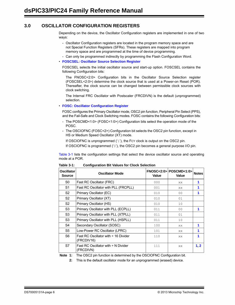
Depending on the device, the Oscillator Configuration registers are implemented in one of twoways:
- Oscillator Configuration registers are located in the program memory space and are not Special Function Registers (SFRs). These registers are mapped into program memory space and are programmed at the time of device programming.
- Can only be programmed indirectly by programming the Flash Configuration Word.
• FOSCSEL: Oscillator Source Selection Register
FOSCSEL selects the initial oscillator source and start-up option. FOSCSEL contains thefollowing Configuration bits:
The FNOSC<2:0> Configuration bits in the Oscillator Source Selection register(FOSCSEL<2:0>) determine the clock source that is used at a Power-on Reset (POR).Thereafter, the clock source can be changed between permissible clock sources withclock switching.
The Internal FRC Oscillator with Postscaler (FRCDIVN) is the default (unprogrammed)selection.
• FOSC: Oscillator Configuration Register
FOSC configures the Primary Oscillator mode, OSC2 pin function, Peripheral Pin Select (PPS),and the Fail-Safe and Clock Switching modes. FOSC contains the following Configuration bits:
- The POSCMD<1:0> (FOSC<1:0>) Configuration bits select the operation mode of the POSC.
- The OSCIOFNC (FOSC<2>) Configuration bit selects the OSC2 pin function, except in HS or Medium Speed Oscillator (XT) mode.
If OSCIOFNC is unprogrammed (‘1’), the FCY clock is output on the OSC2 pin.
If OSCIOFNC is programmed (‘0’), the OSC2 pin becomes a general purpose I/O pin.
Table 3-1 lists the configuration settings that select the device oscillator source and operatingmode at a POR.
Table 3-1: Configuration Bit Values for Clock Selection
Oscillator Source
Oscillator ModeFNOSC<2:0>
ValuePOSCMD<1:0>
ValueNotes
S0 Fast RC Oscillator (FRC) 000 xx 1
S1 Fast RC Oscillator with PLL (FRCPLL) 001 xx 1
S2 Primary Oscillator (EC) 010 00 1
S2 Primary Oscillator (XT) 010 01
S2 Primary Oscillator (HS) 010 10
S3 Primary Oscillator with PLL (ECPLL) 011 00 1
S3 Primary Oscillator with PLL (XTPLL) 011 01
S3 Primary Oscillator with PLL (HSPLL) 011 10
S4 Secondary Oscillator (SOSC) 100 xx 1
S5 Low-Power RC Oscillator (LPRC) 101 xx 1
S6 Fast RC Oscillator with ÷ 16 Divider (FRCDIV16)
110 xx 1
S7 Fast RC Oscillator with ÷ N Divider (FRCDIVN)
111 xx 1, 2
Note 1: The OSC2 pin function is determined by the OSCIOFNC Configuration bit.
2: This is the default oscillator mode for an unprogrammed (erased) device.
These Special Function Registers provide run-time control and status of the oscillator system:
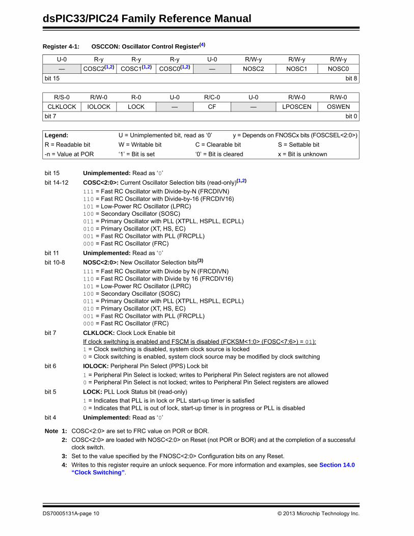
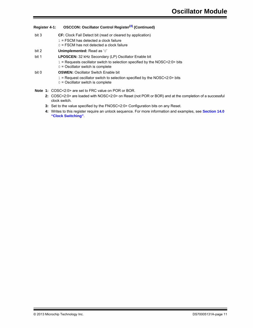
• OSCCON: Oscillator Control Register(4)
This register controls clock switching and provides status information that allows currentclock source, PLL lock and clock fail conditions to be monitored.
• CLKDIV: Clock Divisor Register
This register controls the Doze mode and selects the PLL prescaler, PLL postscaler andFRC postscaler.
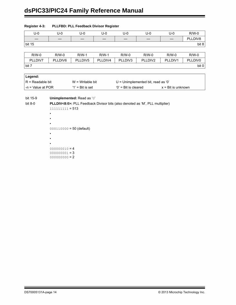
• PLLFBD: PLL Feedback Divisor Register
This register selects the PLL feedback divisor.
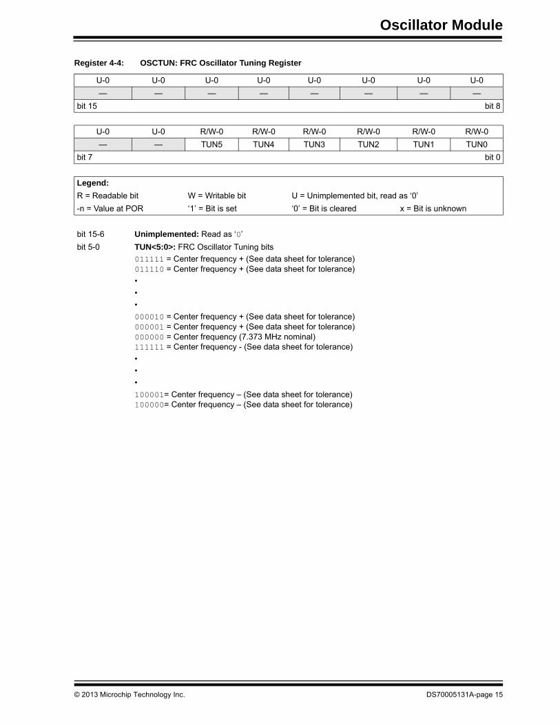
• OSCTUN: FRC Oscillator Tuning Register
This register is used to tune the Internal FRC oscillator frequency in software.
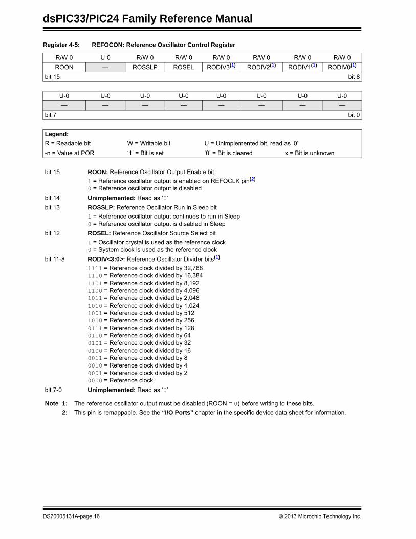
• REFOCON: Reference Oscillator Control Register
This register controls the reference oscillator output.
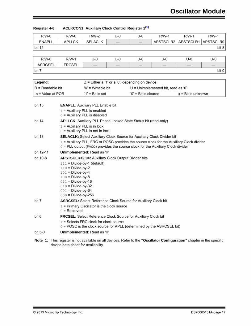
• ACLKCON1: Auxiliary Clock Control Register 1(1)
This register enables and controls the PLL Auxiliary Oscillator.
• ACLKCON3: Auxiliary Clock Control Register 3(1)
This register controls and provides prescalar and postscalar values for the Auxiliary PLLmodule.
• ACLKDIV3: Auxiliary Clock Divisor Control Register 3(1)
This register selects the PLL feedback divisor for the Auxiliary PLL module.
Legend: U = Unimplemented bit, read as ‘0’ y = Depends on FNOSCx bits (FOSCSEL<2:0>)
R = Readable bit W = Writable bit C = Clearable bit S = Settable bit
-n = Value at POR ‘1’ = Bit is set ‘0’ = Bit is cleared x = Bit is unknown
bit 15 Unimplemented: Read as ‘0’
bit 14-12 COSC<2:0>: Current Oscillator Selection bits (read-only)(1,2)
111 = Fast RC Oscillator with Divide-by-N (FRCDIVN)110 = Fast RC Oscillator with Divide-by-16 (FRCDIV16)101 = Low-Power RC Oscillator (LPRC)100 = Secondary Oscillator (SOSC)011 = Primary Oscillator with PLL (XTPLL, HSPLL, ECPLL)010 = Primary Oscillator (XT, HS, EC)001 = Fast RC Oscillator with PLL (FRCPLL)000 = Fast RC Oscillator (FRC)
bit 11 Unimplemented: Read as ‘0’
bit 10-8 NOSC<2:0>: New Oscillator Selection bits(3)
111 = Fast RC Oscillator with Divide by N (FRCDIVN)110 = Fast RC Oscillator with Divide by 16 (FRCDIV16)101 = Low-Power RC Oscillator (LPRC)100 = Secondary Oscillator (SOSC)011 = Primary Oscillator with PLL (XTPLL, HSPLL, ECPLL)010 = Primary Oscillator (XT, HS, EC)001 = Fast RC Oscillator with PLL (FRCPLL)000 = Fast RC Oscillator (FRC)
bit 7 CLKLOCK: Clock Lock Enable bit
If clock switching is enabled and FSCM is disabled (FCKSM<1:0> (FOSC<7:6>) = 01):1 = Clock switching is disabled, system clock source is locked0 = Clock switching is enabled, system clock source may be modified by clock switching
bit 6 IOLOCK: Peripheral Pin Select (PPS) Lock bit
1 = Peripheral Pin Select is locked; writes to Peripheral Pin Select registers are not allowed0 = Peripheral Pin Select is not locked; writes to Peripheral Pin Select registers are allowed
bit 5 LOCK: PLL Lock Status bit (read-only)
1 = Indicates that PLL is in lock or PLL start-up timer is satisfied0 = Indicates that PLL is out of lock, start-up timer is in progress or PLL is disabled
bit 4 Unimplemented: Read as ‘0’
Note 1: COSC<2:0> are set to FRC value on POR or BOR.
2: COSC<2:0> are loaded with NOSC<2:0> on Reset (not POR or BOR) and at the completion of a successful clock switch.
3: Set to the value specified by the FNOSC<2:0> Configuration bits on any Reset.
4: Writes to this register require an unlock sequence. For more information and examples, see Section 14.0 “Clock Switching”.
R = Readable bit W = Writable bit U = Unimplemented bit, read as ‘0’
-n = Value at POR ‘1’ = Bit is set ‘0’ = Bit is cleared x = Bit is unknown
bit 15 ROI: Recover on Interrupt bit
1 = Interrupts will clear the DOZEN bit and the processor clock, and the peripheral clock ratio is set to 1:10 = Interrupts have no effect on the DOZEN bit
bit 14-12 DOZE<2:0>: Processor Clock Reduction Select bits(2,3)
111 = FCY divided by 128110 = FCY divided by 64101 = FCY divided by 32100 = FCY divided by 16011 = FCY divided by 8 (default)010 = FCY divided by 4001 = FCY divided by 2000 = FCY divided by 1
bit 11 DOZEN: Doze Mode Enable bit(1)
1 = DOZE<2:0> field specifies the ratio between the peripheral clocks and the processor clocks0 = Processor clock and peripheral clock ratio are forced to 1:1
bit 10-8 FRCDIV<2:0>: Internal Fast RC Oscillator Postscaler bits
111 = FRC divided by 256110 = FRC divided by 64101 = FRC divided by 32100 = FRC divided by 16011 = FRC divided by 8010 = FRC divided by 4001 = FRC divided by 2000 = FRC divided by 1 (default)
bit 7-6 PLLPOST<1:0>: PLL VCO Output Divider Select bits (also denoted as ‘N2’, PLL postscaler)
11 = Output divided by 810 = Reserved01 = Output divided by 4 (default)00 = Output divided by 2
bit 5 Unimplemented: Read as ‘0’
Note 1: This bit is cleared when the ROI bit is set and an interrupt occurs.
2: The DOZE<2:0> bits can only be written when the DOZEN bit is clear. If DOZEN = 1, any writes to DOZE<2:0> are ignored.
3: The DOZEN bit cannot be set if DOZE<2:0> = 000. If DOZE<2:0> = 000, any attempt by user software to set the DOZEN bit is ignored.
R = Readable bit W = Writable bit U = Unimplemented bit, read as ‘0’
-n = Value at POR ‘1’ = Bit is set ‘0’ = Bit is cleared x = Bit is unknown
bit 15-6 Unimplemented: Read as ‘0’
bit 5-0 TUN<5:0>: FRC Oscillator Tuning bits
011111 = Center frequency + (See data sheet for tolerance)011110 = Center frequency + (See data sheet for tolerance)
•
•
•
000010 = Center frequency + (See data sheet for tolerance)000001 = Center frequency + (See data sheet for tolerance)000000 = Center frequency (7.373 MHz nominal)111111 = Center frequency - (See data sheet for tolerance)
•
•
•
100001= Center frequency – (See data sheet for tolerance)100000= Center frequency – (See data sheet for tolerance)
Legend: Z = Either a ‘1’ or a ‘0’, depending on device
R = Readable bit W = Writable bit U = Unimplemented bit, read as ‘0’
-n = Value at POR ‘1’ = Bit is set ‘0’ = Bit is cleared x = Bit is unknown
bit 15 ENAPLL: Auxiliary PLL Enable bit
1 = Auxiliary PLL is enabled0 = Auxiliary PLL is disabled
bit 14 APLLCK: Auxiliary PLL Phase Locked State Status bit (read-only)
1 = Auxiliary PLL is in lock0 = Auxiliary PLL is not in lock
bit 13 SELACLK: Select Auxiliary Clock Source for Auxiliary Clock Divider bit
1 = Auxiliary PLL, FRC or POSC provides the source clock for the Auxiliary Clock divider0 = PLL output (FVCO) provides the source clock for the Auxiliary Clock divider
bit 12-11 Unimplemented: Read as ‘0’
bit 10-8 APSTSCLR<2:0>: Auxiliary Clock Output Divider bits
bit 7 ASRCSEL: Select Reference Clock Source for Auxiliary Clock bit
1 = Primary Oscillator is the clock source0 = Reserved
bit 6 FRCSEL: Select Reference Clock Source for Auxiliary Clock bit
1 = Selects FRC clock for clock source0 = POSC is the clock source for APLL (determined by the ASRCSEL bit)
bit 5-0 Unimplemented: Read as ‘0’
Note 1: This register is not available on all devices. Refer to the “Oscillator Configuration” chapter in the specific device data sheet for availability.
R = Readable bit W = Writable bit U = Unimplemented bit, read as ‘0’
-n = Value at POR ‘1’ = Bit is set ‘0’ = Bit is cleared x = Bit is unknown
bit 15 ENAPLL: Enable Auxiliary PLL (APLL) and Select APLL as USB Clock Source bit
1 = APLL is enabled, the USB clock source is the APLL output0 = APLL is disabled, the USB clock source is the input clock to the APLL
bit 14 Unimplemented: Read as ‘0’
bit 13 SELACLK: Select Auxiliary Clock Source for Auxiliary Clock Divider bit
1 = Auxiliary PLL or oscillators provide the source clock for the Auxiliary Clock divider0 = Primary PLL provides the source clock for the Auxiliary Clock divider
bit 12-11 AOSCMD<1:0>: Auxiliary Oscillator Mode bits
bit 10 ASRCSEL: Select Reference Clock Source for APLL bit
1 = Primary Oscillator is the clock source for APLL0 = Auxiliary Oscillator is the clock source for APLL
bit 9 FRCSEL: Select FRC as Reference Clock Source for APLL bit
1 = FRC is the clock source for APLL0 = Auxiliary Oscillator or Primary Oscillator is the clock source for APLL (determined by ASRCSEL bit)
bit 8 Unimplemented: Read as ‘0’
bit 7-5 APLLPOST<2:0>: Select PLL VCO Output Divider bits
111 = Divided by 2110 = Divided by 2101 = Divided by 4100 = Divided by 8011 = Divided by 16010 = Divided by 32001 = Divided by 64000 = Divided by 256 (default)
bit 4-3 Unimplemented: Read as ‘0’
bit 2-0 APLLPRE<2:0>: PLL Phase Detector Input Divider bits
111 = Divided by 12110 = Divided by 10101 = Divided by 6100 = Divided by 5011 = Divided by 4010 = Divided by 3001 = Divided by 2000 = Divided by 1 (default)
Note 1: This register is not available on all devices. Refer to the “Oscillator Configuration” chapter in the specific device data sheet for availability.
Oscillator Module
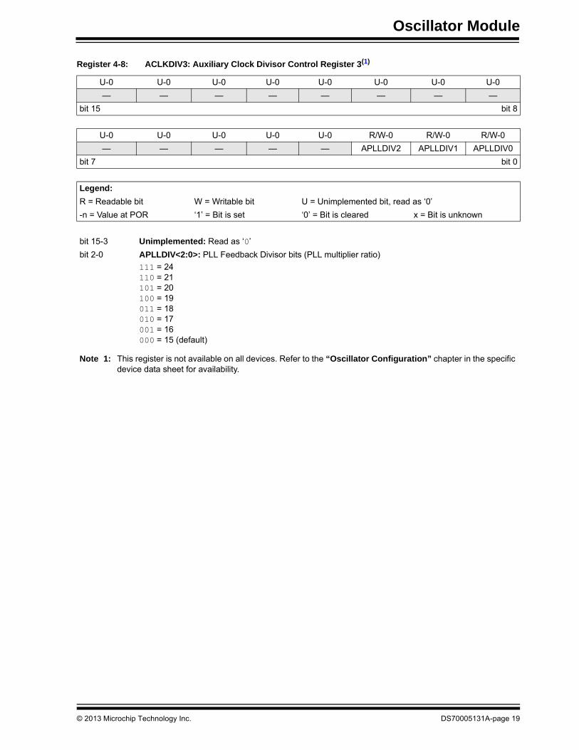
Register 4-8: ACLKDIV3: Auxiliary Clock Divisor Control Register 3(1)
U-0 U-0 U-0 U-0 U-0 U-0 U-0 U-0
— — — — — — — —
bit 15 bit 8
U-0 U-0 U-0 U-0 U-0 R/W-0 R/W-0 R/W-0
— — — — — APLLDIV2 APLLDIV1 APLLDIV0
bit 7 bit 0
Legend:
R = Readable bit W = Writable bit U = Unimplemented bit, read as ‘0’
-n = Value at POR ‘1’ = Bit is set ‘0’ = Bit is cleared x = Bit is unknown
bit 15-3 Unimplemented: Read as ‘0’
bit 2-0 APLLDIV<2:0>: PLL Feedback Divisor bits (PLL multiplier ratio)
Note 1: This register is not available on all devices. Refer to the “Oscillator Configuration” chapter in the specific device data sheet for availability.
The Primary Oscillator (POSC) is available on the OSC1 and OSC2 pins of the dsPIC33/PIC24family devices. This connection enables an external crystal (or ceramic resonator) to provide theclock to the device. Optionally, and depending on the device, it can be used with the internal PLLto boost the system frequency (FOSC) up to 140 MHz for 70 MIPS execution. The PrimaryOscillator provides three modes of operation:
• Medium Speed Oscillator (XT Mode)
The XT mode is a Medium Gain, Medium Frequency mode used to work with crystalfrequencies of 3.5 MHz to 10 MHz.
• High-Speed Oscillator (HS Mode)
The HS mode is a High Gain, High-Frequency mode used to work with crystal frequenciesof 10 MHz to 40 MHz.
• External Clock Source Operation (EC Mode)
If the on-chip oscillator is not used, the EC mode allows the internal oscillator to bebypassed. The device clocks are generated from an external source (0 MHz to up to60 MHz) and input on the OSC1 pin.
The FNOSC<2:0> Configuration bits in the Oscillator Source Selection register(FOSCSEL<2:0>) specify the Primary Oscillator clock source at Power-on Reset. ThePOSCMD<1:0> Configuration bits in the Oscillator Configuration register (FOSC<1:0>) specifythe Primary Oscillator mode. Table 5-1 provides the options selected by specific bitconfigurations, which are programmed at the time of device programming.
Figure 5-1 is a recommended crystal oscillator circuit diagram for the dsPIC33/PIC24 familydevices. Capacitors, C1 and C2, form the Load Capacitance for the crystal. The optimum LoadCapacitance (CL) for a given crystal is specified by the crystal manufacturer. Load Capacitancecan be calculated as shown in Equation 5-1.
Figure 5-1: Crystal or Ceramic Resonator Operation (XT or HS Oscillator Mode)
Assuming C1 = C2, Equation 5-2 gives the capacitor value (C1, C2) for a given load and straycapacitance.
Equation 5-2: External Capacitor for Crystal
For more information on crystal oscillators and their operation, refer to Section 19.0 “RelatedApplication Notes”.
5.1 Oscillator Start-up Time
As the device voltage increases from VSS, the oscillator will start its oscillations. The timerequired for the oscillator to start oscillating depends on these factors:
• Crystal and resonator frequency
• Capacitor values used (C1 and C2 in Figure 5-1)
• Device VDD rise time
• System temperature
• Series resistor value and type if used
• Oscillator mode selection of device (selects the gain of the internal oscillator inverter)
• Crystal quality
• Oscillator circuit layout
• System noise
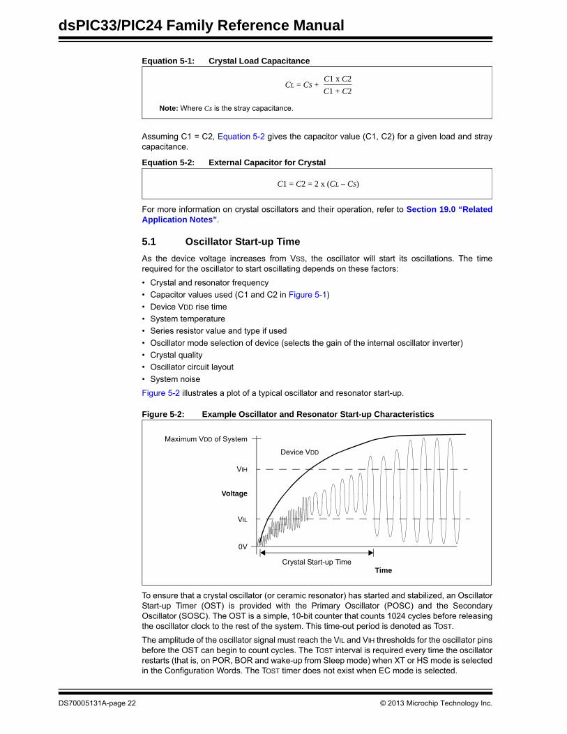
Figure 5-2 illustrates a plot of a typical oscillator and resonator start-up.
Figure 5-2: Example Oscillator and Resonator Start-up Characteristics
To ensure that a crystal oscillator (or ceramic resonator) has started and stabilized, an OscillatorStart-up Timer (OST) is provided with the Primary Oscillator (POSC) and the SecondaryOscillator (SOSC). The OST is a simple, 10-bit counter that counts 1024 cycles before releasingthe oscillator clock to the rest of the system. This time-out period is denoted as TOST.
The amplitude of the oscillator signal must reach the VIL and VIH thresholds for the oscillator pinsbefore the OST can begin to count cycles. The TOST interval is required every time the oscillatorrestarts (that is, on POR, BOR and wake-up from Sleep mode) when XT or HS mode is selectedin the Configuration Words. The TOST timer does not exist when EC mode is selected.
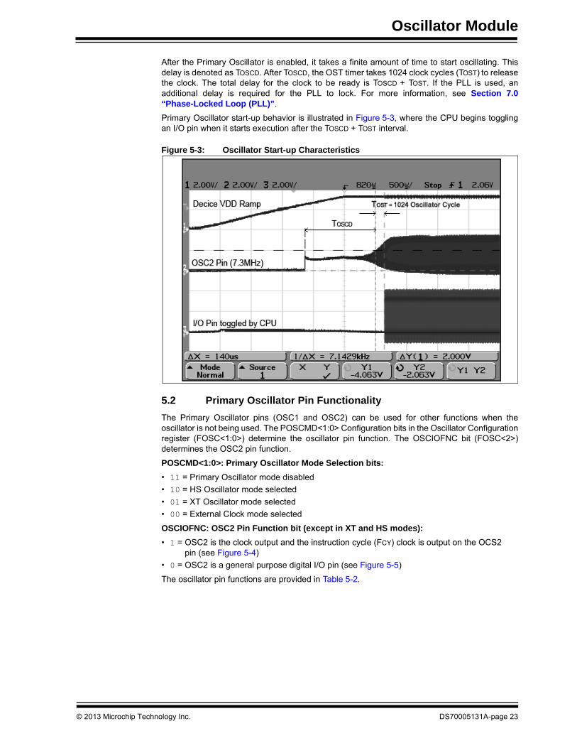
After the Primary Oscillator is enabled, it takes a finite amount of time to start oscillating. Thisdelay is denoted as TOSCD. After TOSCD, the OST timer takes 1024 clock cycles (TOST) to releasethe clock. The total delay for the clock to be ready is TOSCD + TOST. If the PLL is used, anadditional delay is required for the PLL to lock. For more information, see Section 7.0“Phase-Locked Loop (PLL)”.
Primary Oscillator start-up behavior is illustrated in Figure 5-3, where the CPU begins togglingan I/O pin when it starts execution after the TOSCD + TOST interval.
Figure 5-3: Oscillator Start-up Characteristics
5.2 Primary Oscillator Pin Functionality
The Primary Oscillator pins (OSC1 and OSC2) can be used for other functions when theoscillator is not being used. The POSCMD<1:0> Configuration bits in the Oscillator Configurationregister (FOSC<1:0>) determine the oscillator pin function. The OSCIOFNC bit (FOSC<2>)determines the OSC2 pin function.
The Internal Fast RC (FRC) oscillator provides a nominal 7.37 MHz clock without requiring anexternal crystal or ceramic resonator, which results in system cost savings for applications thatdo not require a precise clock reference.
The application software can tune the frequency of the oscillator using the FRC Oscillator Tuningbits (TUN<5:0>) in the FRC Oscillator Tuning register (OSCTUN<5:0>).
The Internal FRC Oscillator starts immediately. Unlike a crystal oscillator, which can take severalmilliseconds to begin oscillation, the Internal FRC starts oscillating immediately.
The Initial Oscillator Source Selection Configuration bits (FNOSC<2:0>) in the Oscillator SourceSelection register (FOSCSEL<2:0>) select the FRC clock source. The FRC clock source optionsat the time of a Power-on Reset are provided in Table 6-1. The Configuration bits areprogrammed at the time of device programming.
6.1 FRC Postscaler Mode (FRCDIVN)
In FRC Postscaler mode, a variable postscaler divides the FRC clock output and allows a lowerfrequency to be chosen. The postscaler is controlled by the Internal Fast RC OscillatorPostscaler bits (FRCDIV<2:0>) in the Clock Divisor register (CLKDIV<10:8>), which allows8 settings, from 1:1 to 1:256, to be chosen.
Optionally, and depending on the device, the FRC postscaler output can be used with the internalPLL to boost the system frequency (FOSC) up to 140 MHz for 70 MIPS instruction cycle executionspeed.
Note: Refer to the “Oscillator Configuration” chapter in the specific device data sheetfor the accuracy of the FRC clock frequency over temperature and voltagevariations.
Table 6-1: FRC Clock Source Options
FNOSC<2:0> Value Primary Oscillator Source and Mode
000 FRC Oscillator (FRC)
001 FRC Oscillator: Postscaler Divide-by-N with PLL (FRCPLL)
Table 6-2: Internal Fast RC Oscillator Postscaler Settings
FRCDIV<2:0> Value Internal FRC Oscillator Settings
000 FRC Divide-by-1 (default)
001 FRC Divide-by-2
010 FRC Divide-by-4
011 FRC Divide-by-8
100 FRC Divide-by-16
101 FRC Divide-by-32
110 FRC Divide-by-64
111 FRC Divide-by-256
Note: The FRC divider should not be changed dynamically when operating in internalFRC with PLL.
To change the FRC divider:1. Switch the clock to non-PLL mode (for example, Internal FRC). 2. Make the necessary changes.3. Switch the clock back to the PLL mode.
The Primary Oscillator and Internal FRC Oscillator sources can optionally use an on-chip PLL toobtain higher operating speeds. Figure 7-1 illustrates a block diagram of the PLL module.
Figure 7-1: dsPIC33/PIC24 Family PLL Block Diagram
For PLL operation, the Phase Frequency Detector (PFD) input frequency and Voltage ControlledOscillator (VCO) output frequency must meet the following requirements at all times, noexceptions:
• The PFD Input Frequency (FPLLI) must be in the range of 0.8 MHz to 8.0 MHz
• The VCO Output Frequency (FVCO) must be in the range of 120 MHz to 340 MHz
The PLL Phase Detector Input Divider Select bits (PLLPRE<4:0>) in the Clock Divisor register(CLKDIV<4:0>) specify the input divider ratio (N1), which is used to scale down the input clock(FIN) to meet the PFD input frequency range of 0.8 MHz to 8.0 MHz.
The PLL Feedback Divisor bits (PLLDIV<8:0>) in the PLL Feedback Divisor register(PLLFBD<8:0>) specify the divider ratio (M), which scales down the VCO Frequency (FVCO) forfeedback to the PFD. The VCO Frequency (FVCO) is ‘M’ times the input reference clock (FPLLI).
The PLL VCO Output Divider Select bits (PLLPOST<1:0>) in the Clock Divisor register(CLKDIV<7:6>) specify the divider ratio (N2) to limit the system clock frequency, FOSC (FPLLO).
Equation 7-1 provides the relation between Input Frequency (FIN) and VCO Frequency (FVCO).
Equation 7-1: FVCO Calculation
Equation 7-2 provides the relation between Input Frequency (FIN) and Output Frequency (FPLLO).
Equation 7-2: FPLLO Calculation
÷ N1
÷ M
÷ N2PFD VCO
PLLPRE<4:0>
PLLDIV<8:0>
PLLPOST<1:0>
0.8 MHz FPLLI(1) 8.0 MHz120 MHZ FVCO(1) 340 MHZ
15 MHz FPLLO(1) 120 MHz @ +125ºC
FIN FPLLI FVCO FPLLO
Note 1: This frequency range must be met at all times.
7.1 Input Clock Limitation at Start-up for PLL Mode
Table 7-1 provides the default values of the PLL Prescaler, PLL Postscaler and PLL FeedbackDivisor Configuration bits at Power-on Reset.
Given these Reset values, the following equations provide the relationship between InputFrequency (FIN) and PFD Input Frequency (FPLLI), VCO Frequency (FVCO) and System ClockFrequency (FOSC) at Power-on Reset.
Equation 7-3: FPLLI at Power-on Reset
Equation 7-4: FVCO at Power-on Reset
Equation 7-5: FPLLO at Power-on Reset
To use the PLL, and to ensure that the PFD Input Frequency (FPLLI) and the VCO frequency arein the specified frequency range to meet the PLL requirements, follow this process:
1. Power up the device with the Internal FRC or the Primary Oscillator without PLL.
2. Change the PLLDIVx, PLLPREx and PLLPOSTx bit values, based on the input frequency,to meet these PLL requirements:
• The PFD Input Frequency (FPLLI) must be in the range of 0.8 MHz to 8.0 MHz
• The VCO Output Frequency (FVCO) must be in the range of 120 MHz to 340 MHz
3. Switch the clock to the PLL mode in software.
Table 7-1: PLL Mode Defaults
Register Bit Field Value at POR Reset PLL Divider Ratio
CLKDIV<4:0> PLLPRE<4:0> 00000 N1 = 2
CLKDIV<7:6> PLLPOST<1:0> 01 N2 = 4
PLLFBD<8:0> PLLDIV<8:0> 000110000 M = 50
Note: Due to the default PLL register setting on Reset, it would violate the OSCspecification to power up with the Primary Oscillator with PLL enabled for inputclock frequencies greater than 13.6 MHz. In that case, the user would need topower up in a non-PLL mode, configure the PLL registers and then perform a clockswitch to a PLL mode.
It is not permitted to directly clock switch from one PLL clock source to a differentPLL clock source. The user would need to transition between PLL clock sourceswith a clock switch to a non-PLL clock source.
Whenever the PLL input frequency, the PLL prescaler or the PLL feedback divisor is changed,the PLL requires a finite amount of time (TLOCK) to synchronize to the new settings.
TLOCK is applied when the PLL is selected as the clock source at Power-on Reset, or during aclock switching operation. The value of TLOCK is relative to the time at which the clock is availableto the PLL input. For example, with the POSC, TLOCK starts after the OST delay. For moreinformation about oscillator start-up delay, see Section 5.1 “Oscillator Start-up Time”. Also,refer to the “Oscillator Configuration” chapter in the specific device data sheet for moreinformation about typical TLOCK values.
The LOCK bit in the Oscillator Control register (OSCCON<5>) is a read-only status bit thatindicates the lock status of the PLL. The LOCK bit is cleared at Power-on Reset, and on a clockswitch operation, when the PLL is selected as the destination clock source. It remains clear whenany clock source not using the PLL is selected. It is advisable to wait for the LOCK bit to be setbefore executing other code after a clock switch event in which the PLL is enabled.
7.2.1 SETUP FOR USING PLL WITH THE PRIMARY OSCILLATOR (POSC)
The following process is used to set up the PLL to operate the device at 60 MIPS with a 10 MHzexternal crystal:
1. To execute instructions at 60 MHz, ensure that the required system clock frequency is:
FOSC = 2 x FCY = 120 MHz
2. To set up the PLL and meet the requirements of the PLL, follow these steps:
a) Select the PLL postscaler to meet the VCO output frequency requirement (120 MHz < FVCO < 340 MHz).
• Select a PLL postscaler ratio of N2 = 2
• Ensure that FVCO = (FPLLO x N2) = 240 MHz
b) Select the PLL prescaler to meet the PFD input frequency requirement (0.8 MHz < FPLLI < 8.0 MHz).
• Select a PLL prescaler ratio of N1 = 2
• Ensure that FPLLI = (FIN ÷ N1) = 5 MHz
c) Select the PLL feedback divisor to generate the required VCO output frequencybased on the PFD input frequency.
• FVCO = FPLLI x M
• M = FVCO ÷ FPLLI = 48
d) Configure the FNOSC<2:0> bits (FOSCSEL<2:0>) to select a clock source withoutthe PLL (for example, Internal FRC) at Power-on Reset.
e) In the main program, change the PLL prescaler, PLL postscaler and PLL feedbackdivisor values to those just decided in the previous steps, and then perform a clockswitch to the PLL mode.
Note: The PLL Prescaler (PLLPREx) and PLL Feedback Divisor (PLLDIVx) bits shouldnot be changed when operating in PLL mode. You must clock switch to a non-PLLmode (e.g., Internal FRC) to make the necessary changes and then clock switchback to the PLL mode.
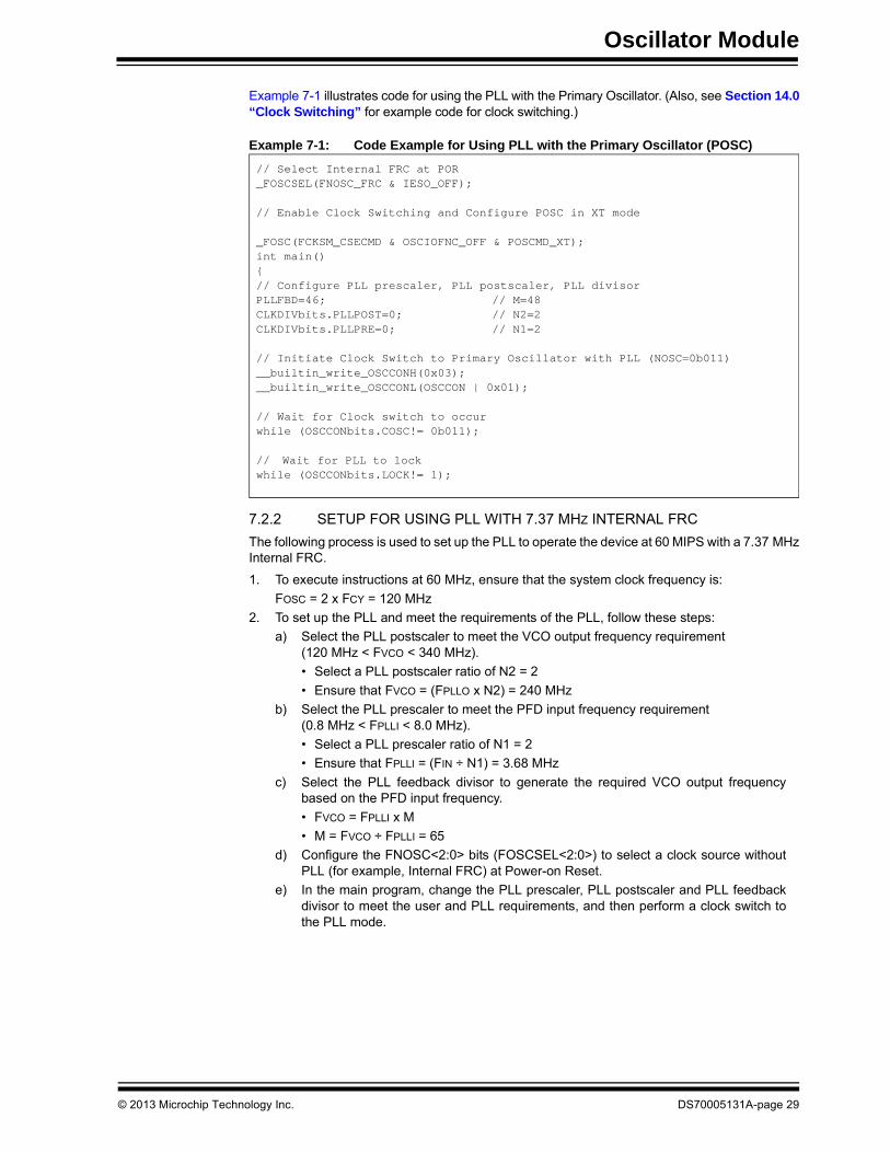
Example 7-1 illustrates code for using the PLL with the Primary Oscillator. (Also, see Section 14.0“Clock Switching” for example code for clock switching.)
Example 7-1: Code Example for Using PLL with the Primary Oscillator (POSC)
7.2.2 SETUP FOR USING PLL WITH 7.37 MHZ INTERNAL FRC
The following process is used to set up the PLL to operate the device at 60 MIPS with a 7.37 MHzInternal FRC.
1. To execute instructions at 60 MHz, ensure that the system clock frequency is:
FOSC = 2 x FCY = 120 MHz
2. To set up the PLL and meet the requirements of the PLL, follow these steps:
a) Select the PLL postscaler to meet the VCO output frequency requirement (120 MHz < FVCO < 340 MHz).
• Select a PLL postscaler ratio of N2 = 2
• Ensure that FVCO = (FPLLO x N2) = 240 MHz
b) Select the PLL prescaler to meet the PFD input frequency requirement (0.8 MHz < FPLLI < 8.0 MHz).
• Select a PLL prescaler ratio of N1 = 2
• Ensure that FPLLI = (FIN ÷ N1) = 3.68 MHz
c) Select the PLL feedback divisor to generate the required VCO output frequencybased on the PFD input frequency.
• FVCO = FPLLI x M
• M = FVCO ÷ FPLLI = 65
d) Configure the FNOSC<2:0> bits (FOSCSEL<2:0>) to select a clock source withoutPLL (for example, Internal FRC) at Power-on Reset.
e) In the main program, change the PLL prescaler, PLL postscaler and PLL feedbackdivisor to meet the user and PLL requirements, and then perform a clock switch tothe PLL mode.
// Select Internal FRC at POR_FOSCSEL(FNOSC_FRC & IESO_OFF);
// Enable Clock Switching and Configure POSC in XT mode
Example 7-2 illustrates code for using PLL with a 7.37 MHz Internal FRC. (See also Section 14.0“Clock Switching” for example code for clock switching.)
Example 7-2: Code Example for Using PLL with 7.37 MHz Internal FRC
// Select Internal FRC at POR_FOSCSEL(FNOSC_FRC & IESO_OFF);
// Enable Clock Switching and Configure Primary Oscillator in XT mode_FOSC(FCKSM_CSECMD & OSCIOFNC_OFF & POSCMD_NONE);
// Initiate Clock Switch to FRC oscillator with PLL (NOSC=0b001)__builtin_write_OSCCONH(0x01);__builtin_write_OSCCONL(OSCCON | 0x01);// Wait for Clock switch to occurwhile (OSCCONbits.COSC!= 0b001);
// Wait for PLL to lockwhile (OSCCONbits.LOCK!= 1);
The Secondary Oscillator (SOSC) enables a 32.768 kHz crystal oscillator to be attached to thedevice as a secondary crystal clock source for low-power operation. It uses the SOSCI andSOSCO pins. The SOSC can also drive Timer1 for Real-Time Clock (RTC) applications.
8.1 SOSC for System Clock
The SOSC is enabled as the system clock when:
• The Initial Oscillator Source Selection Configuration bits (FNOSC<2:0>) in the Oscillator Source Selection register (FOSCSEL<2:0>) are appropriately set to select the SOSC at a POR
• The user-assigned software initiates a clock switch to the SOSC for low-power operation
When the SOSC is not being used to provide the system clock, or the device enters Sleep mode,the SOSC is disabled to save power.
8.2 SOSC Start-up Delay
When the SOSC is enabled, it takes a finite amount of time to start oscillating. For moreinformation, refer to Section 5.1 “Oscillator Start-up Time”.
8.3 Continuous SOSC Operation
Optionally, you can leave the SOSC running continuously. The SOSC is always enabled if theSecondary Oscillator Enable bit (LPOSCEN) is set in the Oscillator Control register(OSCCON<1>).
There are two reasons to leave the SOSC running:
• Keeping the SOSC always ON allows a fast switch to the 32 kHz system clock for lower power operation, since returning to the faster main oscillator still requires an oscillator start-up time if it is a crystal type source. For more information, refer to Section 5.1 “Oscillator Start-up Time”.
• The oscillator should remain on continuously when Timer1 is used as an RTC.
Note 1: The SOSC is sometimes referred to as the Low-Power Secondary Oscillator dueto its low-power capabilities. However, this oscillator should not be confused withthe Low-Power RC (LPRC) Oscillator.
2: This oscillator is not available on all devices. Refer to the specific device data sheetfor more information.
Note: In Sleep mode, all clock sources (the POSC, Internal FRC Oscillator and LPRCOscillator) are shut down, with the exception of the SOSC and LPRC under certainconditions. If the Watchdog Timer is enabled, LPRC is always active, even duringSleep mode. The SOSC can be active in Sleep mode if the Secondary OscillatorEnable bit (LPOSCEN) is set in the Oscillator Control register (OSCCON<1>).
The Low-Power RC (LPRC) Oscillator provides a nominal clock frequency of 32 kHz. The LPRCis the clock source for the Power-up Timer (PWRT), Watchdog Timer (WDT) and Fail-Safe ClockMonitor (FSCM) circuits. It can also be used to provide a low-frequency clock source option forthe device in those applications where power consumption is critical and timing accuracy is notrequired.
9.1 LPRC Oscillator for System Clock
The LPRC oscillator is selected as the system clock when:
• The Initial Oscillator Source Selection bits (FNOSC<2:0>) in the Oscillator Source Selection register (FOSCSEL<2:0>) are appropriately set to select the LPRC Oscillator at Power-on Reset
• User-assigned software initiates a clock switch to the LPRC Oscillator for low-power operation
9.2 Enabling the LPRC Oscillator
The LPRC Oscillator is the clock source for the PWRT, WDT and FSCM. The LPRC Oscillator isenabled at Power-on Reset, if the Power-on Reset Timer Value Select bits (FPWRT<2:0>) in thePOR Configuration Fuse register (FPOR<2:0>) are programmed to a non-zero value.
The LPRC oscillator remains enabled under these conditions:
• The FSCM is enabled• The WDT is enabled• The LPRC Oscillator is selected as the system clock
If none of these conditions is true, the LPRC Oscillator shuts off after the PWRT expires. TheLPRC Oscillator is shut off in Sleep mode.
9.3 LPRC Oscillator Start-up Delay
The LPRC Oscillator starts up immediately, unlike a crystal oscillator, which can take severalmilliseconds to begin oscillation.
Note: The clock frequency of the LPRC Oscillator will vary depending on the devicevoltage and operating temperature. Refer to the “Electrical Characteristics”section in the specific device data sheet for more information.
Note: The LPRC is enabled and running automatically if either WDT or clock fail detect isenabled. The LPRC runs in Sleep mode only if the Watchdog Timer is enabled.Under all other conditions, LPRC is disabled in Sleep mode.
The Auxiliary Oscillator (AOSC) is used by the Universal Serial Bus (USB) module, which needsto operate at a frequency unrelated to the system clock. The Auxiliary Oscillator can use one ofthe following as its clock source:
• Crystal (XT): Crystal and ceramic resonators in the range of 3.5 MHz to 10 MHz.
• High-Speed Crystal (HS): Crystals in the range of 10 MHz to 40 MHz. The external crystal is connected to the SOSCI and SOSCO pins.
• External Clock (EC): External clock signal up to 60 MHz. The external clock signal is directly applied to the SOSCI pin.
10.1 Enabling the Auxiliary Oscillator
To enable the Auxiliary Oscillator mode, the Enable Auxiliary PLL bit (ENAPLL) must be set inthe Auxiliary Clock Control register (ACLKCONx<15>). The Auxiliary Oscillator Mode bits(AOSCMD<1:0>) allow four oscillator mode settings, as listed in Table 10-1.
Table 10-1: Auxiliary Oscillator and External Oscillator Mode Settings
10.2 Auxiliary Clock Source
The desired reference clock source for the Auxiliary PLL can be selected by setting theappropriate clock source select bits in the Auxiliary Clock Control Register 1 (ACLKCON1).
Set the Auxiliary Reference Clock Select bit (ASRCSEL) to use the Primary Oscillator as theclock source or clear this bit to use the Auxiliary Oscillator as the clock source.
Set the FRC Select bit (FRCSEL) to use the FRC as the clock source, or clear this bit to use theAuxiliary or Primary Oscillator selected by the ASRCSEL bit as the clock source.
Set the Select Clock Source to Auxiliary Clock Divider bit (SELACLK) in the Auxiliary ClockControl Register 1 (ACLKCON1) to select the Auxiliary PLL or oscillators to provide the clocksource for the Auxiliary Clock divider.
Clearing the SELACLK bit will cause the primary PLL output to act as the clock source to theAuxiliary Clock divider.
Note: This feature is not available on all devices. Refer to the “Oscillator Configuration”chapter in the specific device data sheet for availability.
The Auxiliary Oscillator uses an on-chip PLL to obtain different Auxiliary Clock speeds.Figure 11-1 shows a block diagram of the APLL module.
Figure 11-1: dsPIC33/PIC24 Family APLL Block Diagram
For operation of the APLL, the Auxiliary Phase Frequency Detector (APFD) input frequency andthe Auxiliary Voltage Controlled Oscillator (AVCO) output frequency must meet the followingrequirements:
• The APFD Input Frequency (AFPLLI) must be in the range of 3 MHz to 5.5 MHz• The AVCO output frequency must be in the range of 60 MHz to 120 MHz
The APLL Phase Detector Input Divider bits (APLLPRE<2:0>) in the Auxiliary Clock ControlRegister 3 (ACLKCON3<2:0>) specify the input divider ratio (N1), which is used to scale down theAuxiliary PLL Input (AFIN) clock to meet the APFD input frequency range of 3 MHz to 5.5 MHz.
The Auxiliary PLL Feedback Divisor bits (APLLDIV<2:0>) in the Auxiliary Clock Divisor ControlRegister 3 (ACLKDIV3<2:0>) specify the divider ratio (M), which scales down the AVCO frequencyfor feedback to the APFD. The AVCO frequency is M times the APFD Input Frequency (AFPLLI).
The APLL VCO Output Divider Select bits (APLLPOST<2:0>) in the Auxiliary Clock ControlRegister 3 (ACLKCON3<7:5>) specify the divider ratio (N2).
The correct combination of the APLL Phase Detector Input Divider bits (APLLPRE<2:0>), theAuxiliary PLL Feedback Divisor bits (APLLDIV<2:0>) and the APLL VCO Output Divider bits(APLLPOST<2:0>) will provide the 48 MHz Auxiliary Clock (ACLK) frequency needed by theUSB module.
Equation 11-1 shows the relationship between the Auxiliary PLL Input (AFIN) clock frequency andthe Auxiliary Clock (ACLK) frequency.
Equation 11-1: ACLK Calculation
Note: This feature is not available on all devices. Refer to the “Oscillator Configuration”chapter in the specific device data sheet for availability.
Note 1: This frequency range must be met at all times.
2: The Auxiliary Oscillator is not available on all devices. Refer to the “Oscillator Configuration” chapter in the specific device data sheet for availability.
48 MHz
(USB)
AuxiliaryOscillator(2)
SecondaryOscillator
SOSCO
SOSCI
3.5 MHz ≤ AUX_FIN(1) ≤ 10 MHz
Note: When APLLDIV<2:0> = 111, substitute (APLLDIV + 15) with (APLLDIV + 18) inEquation 11-1.
Equation 11-2 shows the relationship between the Auxiliary PLL Input (AFIN) clock frequency andthe AVCO Frequency.
Equation 11-2: AVCO Calculation
11.1 APLL Setup
11.1.1 SETUP FOR USING APLL WITH AUXILIARY OSCILLATOR WITH AN 8 MHz CRYSTAL
1. Clear the ASRCSEL bit to choose the Auxiliary Oscillator as the clock source for the APLL.
2. Clear the FRCSEL bit to choose the Auxiliary Oscillator at the clock source for the APLL.
3. Set the SELACLK bit to choose the Auxiliary PLL or oscillators to provide the source clockfor the Auxiliary Clock divider.
4. Follow these steps to configure the APLL Phase Detector Input Divider bits(APLLPRE<2:0>), the Auxiliary PLL Feedback Divisor bits (APLLDIV<2:0>) and the APLLVCO Output Divider bits (APLLPOST<2:0>) to set up the APLL for a 48 MHz ACLK (usedby the USB module) using an 8 MHz Auxiliary Oscillator:
a) Select the APLL VCO output divider to meet the AVCO output frequency requirement(60 MHz < AVCO < 120 MHz).
• Select an APLL VCO output divider ratio of N2 = 2
• Ensure that AVCO = (ACLK x N2) = 96 MHz
b) Select the APLL phase detector input divider to meet the APFD input frequencyrequirement (3 MHz < AFPLLI < 5.5 MHz).
• Select an APLL phase detector input divider ratio of N1 = 2
• Ensure that AFPLLI = (AFIN N1) = 4 MHz
c) Select the Auxiliary PLL feedback divisor to generate the required VCO outputfrequency based on the PFD input frequency.
• AVCO = AFPLLI x M
• M = AVCO AFPLLI = 24
5. Enable the Auxiliary PLL by setting the ENAPLL bit.
Example 11-1 provides code for using the APLL with the Auxiliary Oscillator.
Example 11-1: Code Example for Using the APLL with the Auxiliary Oscillator
Note: This feature is not available on all devices. Refer to the “Oscillator Configuration”chapter in the specific device data sheet for availability.
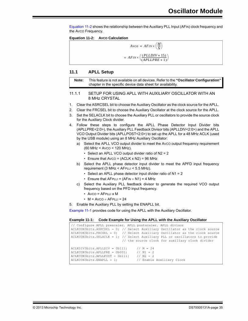
Avco AFINMN----- =
AFINPLLDIV 15+ APLLPRE 1+
----------------------------------------- =
// Configure APLL prescaler, APLL postscaler, APLL divisorACLKCON3bits.ASRCSEL = 0; // Select Auxiliary Oscillator as the clock sourceACLKCON3bits.FRCSEL = 0; // Select Auxiliary Oscillator as the clock sourceACLKCON3bits.SELACLK = 1; // Select Auxiliary PLL or oscillators to provide
11.1.2 SETUP FOR USING APLL WITH PRIMARY OSCILLATOR USING AN 8 MHz CRYSTAL
1. Set the ASRCSEL bit to choose the Primary Oscillator as the clock source for the APLL.
2. Clear the FRCSEL bit to choose the Primary Oscillator as the clock source for the APLL.
3. Set the SELACLK bit to choose the Auxiliary PLL or oscillators to provide the clock sourcefor the Auxiliary Clock divider.
4. Follow these steps to configure the APLL Phase Detector Input Divider bits(APLLPRE<2:0>), the Auxiliary PLL Feedback Divisor bits (APLLDIV<2:0>) and the APLLVCO Output Divider bits (APLLPOST<2:0>) to set up the APLL for a 48 MHz ACLK (usedby the USB module) using an 8 MHz Auxiliary Oscillator:
a) Select the APLL VCO output divider to meet the AVCO output frequency requirement(60 MHz < AVCO < 120 MHz).
• Select an APLL VCO output divider ratio of N2 = 2
• Ensure that AVCO = (ACLK x N2) = 96 MHz
b) Select the APLL phase detector input divider to meet the APFD input frequencyrequirement (3 MHz < AFPLLI < 5.5 MHz).
• Select an APLL phase detector input divider ratio of N1 = 2
• Ensure that AVCO = (AFIN N1) = 4 MHz
c) Select the Auxiliary PLL feedback divisor to generate the required VCO outputfrequency based on the PFD input frequency.
• AVCO = AFPLLI x M
• M = AVCO AFPLLI = 24
5. Enable the Auxiliary PLL by setting the ENAPLL bit.
Example 11-2 provides code for using the APLL with the Primary Oscillator.
Example 11-2: Code Example for Using the APLL with the Primary Oscillator
// Configure APLL prescaler, APLL postscaler, APLL divisorACLKCON3bits.ASRCSEL = 1; // Select Primary Oscillator as the clock sourceACLKCON3bits.FRCSEL = 0; // Select Primary Oscillator as the clock sourceACLKCON3bits.SELACLK = 1; // Select Auxiliary PLL or oscillators to provide
The Auxiliary PLL can be used to provide a high-speed clock to peripherals, such as the PWMand the ADC. The ACLKCON register selects the reference clock and output dividers forobtaining the necessary Auxiliary Clock for the PWM and ADC modules. The Auxiliary Clock forthe PWM and ADC can be either the:
• Internal FRC Oscillator (7.37 MHz nominal)
• Primary Oscillator
• Internal FRC Oscillator with PLL
• Primary Oscillator with PLL
• Auxiliary PLL
12.1 Enabling the Auxiliary PLL
To enable the Auxiliary PLL, the following steps must be performed:
1. Select the reference clock for the Auxiliary PLL by setting the ASRCSEL bit(ACLKCON<7>) for the POSC or by setting the FRCSEL bit (ACLKCON<6>) for theInternal FRC Oscillator.
2. Enable the Auxiliary PLL by setting the ENAPLL bit (ACLKCON<15>).
3. Select the clock source for the Auxiliary Clock output divider by setting the SELACLK bit(ACLKCON<13>).
4. Select the appropriate clock divider by setting the APSTSCLR<2:0> bits(ACLKCON<10:8>).
5. Ensure that the Auxiliary PLL has locked and is ready for operation. This is done by pollingthe APLLCK bit (ACLKCON<14>).
Example 12-1 illustrates a code example to set up the Auxiliary PLL for 120 MHz, using theInternal FRC Oscillator as a clock reference.
Example 12-1: Enabling the Auxiliary PLL
Note: This feature is not available on all devices. Refer to the “Oscillator Configuration”chapter in the specific device data sheet for availability.
ACLKCONbits.FRCSEL = 1; /* Internal FRC is clock source for auxiliary PLL */ACLKCONbits.ENAPLL = 1; /* APLL is enabled */ACLKCONbits.SELACLK = 1; /* Auxiliary PLL provides the source clock for the */
while(ACLKCONbits.APLLCK != 1); /* Wait for Auxiliary PLL to Lock */
/* With 7.37 MHz FRC input selection, the Auxiliary Clock output will be 16x7.37 MHz = 118 MHz. */
Note 1: If the Primary PLL is used as a source for the Auxiliary Clock, then the Primary PLLshould be configured to a maximum operation of up to 30 MIPS or less.
2: To achieve 1.04 ns PWM resolution, the Auxiliary Clock must use the x16 AuxiliaryPLL and be set up for 120 MHz. All other clock sources will have a minimum PWMresolution of 8 ns.
3: By using various combinations of clock inputs and PLL settings, it is possible to con-figure the oscillator out of specification. The user-assigned software must ensurethat the Auxiliary Clock is configured to be within the electrical specification range of112 MHz to 120 MHz.
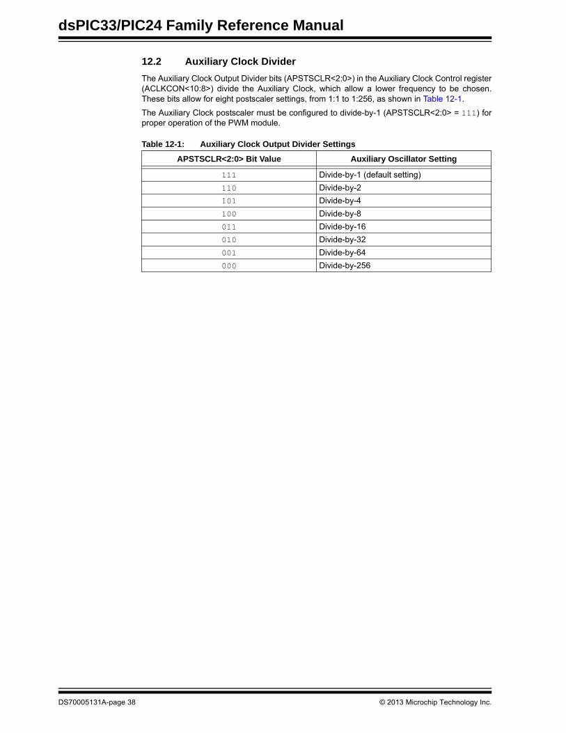
The Auxiliary Clock Output Divider bits (APSTSCLR<2:0>) in the Auxiliary Clock Control register(ACLKCON<10:8>) divide the Auxiliary Clock, which allow a lower frequency to be chosen.These bits allow for eight postscaler settings, from 1:1 to 1:256, as shown in Table 12-1.
The Auxiliary Clock postscaler must be configured to divide-by-1 (APSTSCLR<2:0> = 111) forproper operation of the PWM module.
The Fail-Safe Clock Monitor (FSCM) allows the device to continue to operate in the event of anoscillator failure. The FSCM function is enabled by programming the Clock Switching ModeConfiguration bits (FCKSM<1:0>) in the Oscillator Configuration register (FOSC<7:6>) at thetime of device programming. When FSCM is enabled (FCKSM<1:0> = 00), the LPRC InternalOscillator will run at all times (except during Sleep mode).
The FSCM monitors the system clock. If it does not detect a system clock within a specific periodof time (typically 2 ms, maximum 4 ms), it generates a clock failure trap and switches the systemclock to the FRC Oscillator. The user-assigned application has the option to either attempt torestart the oscillator or execute a controlled shutdown.
The FSCM module takes the following actions when it switches to the FRC Oscillator:
• The Current Oscillator Selection bits, COSC<2:0> (OSCCON<14:12>), are loaded with ‘000’ (Internal FRC).
• The Clock Fail (CF) detect bit (OSCCON<3>) is set to indicate the clock failure.
• The Oscillator Switch Enable (OSWEN) control bit (OSCCON<0>) is cleared to cancel any pending clock switches.
13.1 FSCM Delay
The FSCM monitors the system clock for activity after the system clock is ready and the nominaldelay (TFSCM) has elapsed.
The FSCM delay (TFSCM) is applied when the FSCM is enabled and the Primary or SecondaryOscillator is selected as the system clock.
For more information, refer to the “dsPIC33E/PIC24E Family Reference Manual”, “Reset”(DS70602). For recent documentation, visit the Microchip web site at www.microchip.com.
13.2 FSCM and WDT
The FSCM and WDT use the LPRC Oscillator as their time base. In the event of a clock failure,the WDT is unaffected and continues to run on the LPRC.
Note: When the device is in Sleep mode, if the clock fails, the FSCM does not wake-upthe device.
Note: Refer to the “Electrical Characteristics” section of the specific device data sheetfor TFSCM values.
Clock switching can be initiated as a result of a hardware event or a software request. A typicalscenario includes:
• Two-Speed Start-up sequence upon Power-on Reset, which initially uses the Internal FRCOscillator for quick start-up and then automatically switches to the selected clock sourcewhen the clock is ready.
• Fail-Safe Clock Monitor automatically switches to the Internal FRC Oscillator on a clock failure.
• User-assigned application software requests clock switching by setting the OSWEN bit(OSCCON<0>), causing the hardware to switch to the clock source selected by theNOSC<2:0> bits (OSCCON<10:8>) when the clock is ready.
In each of these cases, the clock switch event assures that the proper make-before-breaksequence is executed. That is, the new clock source is ready before the old clock is deactivatedand code continues to execute as clock switching occurs.
dsPIC33/PIC24 family devices feature the Phase-Locked Loop Enable (PLLKEN) bit in theOscillator Configuration register (FOSC<8>). Setting this bit will cause the device to wait until thePLL locks before switching to the PLL clock source. When this bit is set to ‘0’, the device will notwait for the PLL lock and will proceed with the clock switch. The default setting for this bit is ‘1’.
With few limitations, applications are free to switch between any of the four clock sources (POSC,SOSC, FRC and LPRC), under software control, at any time. To limit the possible side effectsthat could result from this flexibility, dsPIC33/PIC24 family devices have a safeguard lock builtinto the switch process. That is, the OSCCON register is write-protected during clock switching.
14.1 Enabling Clock Switching
The Clock Switching Mode Configuration bits (FCKSM<1:0>) in the Oscillator Configurationregister (FOSC<7:6>) must be programmed to enable clock switching and the Fail-Safe ClockMonitor (see Table 14-1).
The first bit determines if clock switching is enabled (‘0’) or disabled (‘1’). The second bitdetermines if the FSCM is enabled (‘0’) or disabled (‘1’). FSCM can only be enabled if clockswitching is also enabled. If clock switching is disabled (‘1’), the value of the second bit is irrelevant.
14.2 Clock Switch Sequence
The recommended process for a clock switch is as follows:
1. Read the COSC<2:0> bits (OSCCON<14:12>) to determine the current oscillator source(if this information is relevant to the application).
2. Execute the unlock sequence to allow a write to the high byte of the OSCCON register.
3. Write the appropriate value to the NOSC<2:0> control bits (OSCCON<10:8>) for the newoscillator source.
4. Execute the unlock sequence to allow a write to the low byte of the OSCCON register.
5. Set the OSWEN bit (OSCCON<0>) to initiate the oscillator switch.
After the previous steps are completed, the clock switch logic performs the following tasks:
1. The clock switching hardware compares the COSC<2:0> status bits (OSCCON<14:12>)with the new value of the NOSC<2:0> control bits (OSCCON<10:8>). If they are the same,the clock switch is a redundant operation. In this case, the OSWEN bit (OSCCON<0>) iscleared automatically and the clock switch is aborted.
2. If a valid clock switch has been initiated, the PLL LOCK (OSCCON<5>) and CF(OSCCON<3>) status bits are cleared.
3. The new oscillator is turned on by the hardware (if it is not running). If a crystal oscillator(the POSC or SOSC) must be turned on, the hardware waits for TOSCD until the crystalstarts oscillating and TOST expires. If the new source uses the PLL, the hardware waitsuntil a PLL lock is detected (OSCCON<5> = 1).
4. The hardware waits for the new clock source to stabilize and then performs the clockswitch.
5. The hardware clears the OSWEN bit (OSCCON<0>) to indicate a successful clocktransition. In addition, the NOSC<2:0> bit (OSCCON<10:8>) values are transferred to theCOSC<2:0> status bits (OSCCON<14:12>).
6. The old clock source is turned off at this time, with the exception of LPRC (if WDT orFSCM is enabled) or SOSC (if SOSCEN remains set). The timing of the transitionbetween clock sources is illustrated in Figure 14-1.
Figure 14-1: Clock Transition Timing Diagram
Note 1: Clock switching between the XT, HS and EC Primary Oscillator modes is notpossible without reprogramming the device.
2: Direct clock switching between PLL modes is not possible. For example, clockswitching should not occur between the Primary Oscillator with PLL and theInternal FRC oscillator with PLL.
3: Setting the CLKLOCK bit (OSCCON<7>) prevents clock switching when clockswitching is enabled and Fail-Safe Clock Monitoring is disabled by Configurationbits, FCKSM<1:0> (FOSC<7:6>) = 01. The CLKLOCK bit cannot be cleared afterit is set by the software; it clears on a Power-on Reset.
4: The processor continues to execute code throughout the clock switchingsequence. Timing-sensitive code should not be executed during this time.
5: The clock switch will not wait for the PLL lock if the PLLKEN bit in the OscillatorConfiguration register (FOSC<8>) is set to ‘0’.
Old Clock Source
New Clock Source
System Clock
OSWEN
New SourceEnabled
New SourceStable Old Source
Disabled
Both Oscillators Active
Note: The system clock can be any selected source – Primary, FRC or LPRC.
When you incorporate clock switching into an application, consider these points when designingthe code:
• The OSCCON unlock sequence is extremely timing critical. The OSCCON register byte isonly writable for one instruction cycle following the sequence. Some high-level languages,such as C, may not preserve the timing-sensitive sequence of instructions when compiled.When clock switching is required for an application written in a high-level language, it isgood to create the routine in assembler and link it to the application, and then call it as afunction when it is required.
• If the destination clock source is a crystal oscillator, the clock switch time will be dominatedby the oscillator start-up time.
• If the new clock source does not start or is not present, the clock switching hardware willcontinue to run from the current clock source. User-assigned software can detect thissituation because the OSWEN bit (OSCCON<0>) remains set indefinitely.
• If the new clock source uses the PLL, a clock switch will not occur until the lock has beenachieved. User-assigned software can detect a loss of PLL lock because the LOCK bit(OSCCON<5>) is cleared and the OSWEN bit (OSCCON<0>) is set.
• Switching to a low-frequency clock source, like the Secondary Oscillator, will result in slowdevice operation.
14.4 Aborting a Clock Switch
If a clock switch does not complete, the clock switch logic can be reset by clearing the OSWENbit (OSCCON<0>). When OSWEN is cleared, the clock switch process is aborted, the OscillatorStart-up Timer (if applicable) is stopped and reset, and the PLL (if applicable) is stopped.
Typical assembly code for aborting a clock switch is shown in Example 14-2. A clock switchprocedure can be aborted at any time. A clock switch that is already in progress can also beaborted by performing a second clock switch.
Example 14-2: Aborting a Clock Switch
14.5 Entering Sleep Mode During a Clock Switch
If the device enters Sleep mode during a clock switch operation, the clock switch operation isaborted. The processor keeps the old clock selection and the OSWEN bit is cleared. The PWRSAVinstruction is then executed normally.
It is useful to perform a clock switch to the Internal FRC Oscillator before entering Sleep mode,as this will ensure fast wake-up from Sleep mode.
MOV #OSCCON,W1 ; pointer to OSCCONMOV.b #0x46,W2 ; first unlock codeMOV.b #0x57,W3 ; second unlock codeMOV.b W2, [W1] ; write first unlock codeMOV.b W3, [W1] ; write second unlock codeBCLR OSCCON,#OSWEN ; ABORT the switch
The Internal External Start-up Option Configuration bit (IESO) in the Oscillator Source Selectionregister (FOSCSEL<7>) specifies whether to start the device with a user-selected oscillatorsource or to initially start with the Internal FRC, and then switch to the user-selected oscillator. Ifthis bit is set to ‘1’, the device will always power up on the Internal FRC Oscillator, regardless ofthe other oscillator source settings (FOSCSEL<2:0>). Then, the device switches to the specifiedoscillator when it is ready.
Unless FSCM is enabled, the FRC Oscillator is turned off immediately after the clock switch iscompleted. The Two-Speed Start-up option is a faster way to get the device up and running, andworks independently from the state of the Clock Switching Mode Configuration bits,FCKSM<1:0> (FOSC<7:6>).
Two-Speed Start-up is useful when an external oscillator is selected by the FNOSC<2:0>Configuration bits (FOSCSEL<2:0>) and a crystal-based oscillator (Primary Oscillator) has alonger start-up time. As an Internal RC Oscillator, the FRC clock source is available immediatelyfollowing a Power-on Reset. With Two-Speed Start-up, the device starts executing code in itsdefault oscillator configuration (FRC). It continues to operate in this mode until the specifiedexternal oscillator source becomes stable, at which time, it switches to that source.
User code can check which clock source is currently providing the device clocking by checkingthe status of the COSC<2:0> bits (OSCCON<14:12>) against the NOSC<2:0> bits(OSCCON<10:8>). If these two sets of bits match, the clock switch has completed successfullyand the device is running from the intended clock source.
16.0 REFERENCE CLOCK OUTPUT
The reference clock output provides a clock signal to any remappable pin (RPn). The referenceclock can be either the Primary Oscillator or the system clock.
The ROSEL bit (REFOCON<12>) in the Reference Oscillator Control register selects betweenthe external oscillator and the system clock.
Figure 1-1 shows a block diagram for the reference clock. See the REFOCON register(Register 4-5) for the bits associated with the reference clock output. Refer to the specific devicedata sheet for more information on peripheral remapping.
17.0 LINEAR FEEDBACK SHIFT REGISTER
Some devices incorporate a Linear Feedback Shift Register (LFSR) which is composed of a15-bit shift register, providing pseudorandom data with 215 – 1 unique values for use by the uservia software. The pseudorandom number generator is incremented on every PWM cycle.
Note: Two-Speed Start-up is redundant if the selected device clock source is FRC.
gend: — = unimplemented, read as ‘0’. Reset values are shown in hexadecimal.
te 1: The OSCCON register Reset values are dependent on the FOSCSEL Configuration bits and by the type of Reset.
ble 18-2: Oscillator Configuration Registers
le Name Bit 15 Bit 14 Bit 13 Bit 12 Bit 11 Bit 10 Bit 9 Bit 8 Bit 7 Bit 6 Bit 5 Bit 4 Bit 3
SCSEL — — — — — — — — IESO — — — —
SC — — — — — — — PLLKEN FCKSM1 FCKSM0 IOL1WAY — —
gend: — = unimplemented, read as ‘0’. Reset values are shown in hexadecimal.
dsPIC33/PIC24 Family Reference Manual
19.0 RELATED APPLICATION NOTES
This section lists application notes that pertain to this section of the manual. These applicationnotes may not be written specifically for the dsPIC33/PIC24 Product Family, but the concepts arepertinent and could be used with modification and possible limitations. The current applicationnotes related to the Oscillator Module include:
Low-Power Design Using PICmicro® Microcontrollers AN606
Crystal Oscillator Basics and Crystal Selection for rfPIC® and PICmicro® Devices AN826
Note: Please visit the Microchip web site (www.microchip.com) for additional applicationnotes and code examples for the dsPIC33/PIC24 family of devices.
Note the following details of the code protection feature on Microchip devices:
• Microchip products meet the specification contained in their particular Microchip Data Sheet.
• Microchip believes that its family of products is one of the most secure families of its kind on the market today, when used in the intended manner and under normal conditions.
• There are dishonest and possibly illegal methods used to breach the code protection feature. All of these methods, to our knowledge, require using the Microchip products in a manner outside the operating specifications contained in Microchip’s Data Sheets. Most likely, the person doing so is engaged in theft of intellectual property.
• Microchip is willing to work with the customer who is concerned about the integrity of their code.
• Neither Microchip nor any other semiconductor manufacturer can guarantee the security of their code. Code protection does not mean that we are guaranteeing the product as “unbreakable.”
Code protection is constantly evolving. We at Microchip are committed to continuously improving the code protection features of ourproducts. Attempts to break Microchip’s code protection feature may be a violation of the Digital Millennium Copyright Act. If such actsallow unauthorized access to your software or other copyrighted work, you may have a right to sue for relief under that Act.
Information contained in this publication regarding deviceapplications and the like is provided only for your convenienceand may be superseded by updates. It is your responsibility toensure that your application meets with your specifications.MICROCHIP MAKES NO REPRESENTATIONS ORWARRANTIES OF ANY KIND WHETHER EXPRESS ORIMPLIED, WRITTEN OR ORAL, STATUTORY OROTHERWISE, RELATED TO THE INFORMATION,INCLUDING BUT NOT LIMITED TO ITS CONDITION,QUALITY, PERFORMANCE, MERCHANTABILITY ORFITNESS FOR PURPOSE. Microchip disclaims all liabilityarising from this information and its use. Use of Microchipdevices in life support and/or safety applications is entirely atthe buyer’s risk, and the buyer agrees to defend, indemnify andhold harmless Microchip from any and all damages, claims,suits, or expenses resulting from such use. No licenses areconveyed, implicitly or otherwise, under any Microchipintellectual property rights.
2013 Microchip Technology Inc.
QUALITY MANAGEMENT SYSTEM CERTIFIED BY DNV
== ISO/TS 16949 ==
Trademarks
The Microchip name and logo, the Microchip logo, dsPIC, FlashFlex, KEELOQ, KEELOQ logo, MPLAB, PIC, PICmicro, PICSTART, PIC32 logo, rfPIC, SST, SST Logo, SuperFlash and UNI/O are registered trademarks of Microchip Technology Incorporated in the U.S.A. and other countries.
FilterLab, Hampshire, HI-TECH C, Linear Active Thermistor, MTP, SEEVAL and The Embedded Control Solutions Company are registered trademarks of Microchip Technology Incorporated in the U.S.A.
Silicon Storage Technology is a registered trademark of Microchip Technology Inc. in other countries.
Analog-for-the-Digital Age, Application Maestro, BodyCom, chipKIT, chipKIT logo, CodeGuard, dsPICDEM, dsPICDEM.net, dsPICworks, dsSPEAK, ECAN, ECONOMONITOR, FanSense, HI-TIDE, In-Circuit Serial Programming, ICSP, Mindi, MiWi, MPASM, MPF, MPLAB Certified logo, MPLIB, MPLINK, mTouch, Omniscient Code Generation, PICC, PICC-18, PICDEM, PICDEM.net, PICkit, PICtail, REAL ICE, rfLAB, Select Mode, SQI, Serial Quad I/O, Total Endurance, TSHARC, UniWinDriver, WiperLock, ZENA and Z-Scale are trademarks of Microchip Technology Incorporated in the U.S.A. and other countries.
SQTP is a service mark of Microchip Technology Incorporated in the U.S.A.
GestIC and ULPP are registered trademarks of Microchip Technology Germany II GmbH & Co. KG, a subsidiary of Microchip Technology Inc., in other countries.
All other trademarks mentioned herein are property of their respective companies.
Microchip received ISO/TS-16949:2009 certification for its worldwide
DS70005131A-page 49
headquarters, design and wafer fabrication facilities in Chandler and Tempe, Arizona; Gresham, Oregon and design centers in California and India. The Company’s quality system processes and procedures are for its PIC® MCUs and dsPIC® DSCs, KEELOQ® code hopping devices, Serial EEPROMs, microperipherals, nonvolatile memory and analog products. In addition, Microchip’s quality system for the design and manufacture of development systems is ISO 9001:2000 certified.
DS70005131A-page 50 2013 Microchip Technology Inc.
AMERICASCorporate Office2355 West Chandler Blvd.Chandler, AZ 85224-6199Tel: 480-792-7200 Fax: 480-792-7277Technical Support: http://www.microchip.com/supportWeb Address: www.microchip.com
AtlantaDuluth, GA Tel: 678-957-9614 Fax: 678-957-1455
BostonWestborough, MA Tel: 774-760-0087 Fax: 774-760-0088
ChicagoItasca, IL Tel: 630-285-0071 Fax: 630-285-0075