CY54FCT480T, CY74FCT480T DUAL 8-BIT PARITY GENERATORS/CHECKERS SCCS025B – MAY 1993 – REVISED OCTOBER 2001 1 POST OFFICE BOX 655303 • DALLAS, TEXAS 75265 Function, Pinout, and Drive Compatible With FCT and F Logic Reduced V OH (Typically = 3.3 V) Versions of Equivalent FCT Functions Edge-Rate Control Circuitry for Significantly Improved Noise Characteristics I off Supports Partial-Power-Down Mode Operation Matched Rise and Fall Times Fully Compatible With TTL Input and Output Logic Levels Two 8-Bit Parity Generators/Checkers Open-Drain Active-Low Parity-Error Output Expandable for Larger Word Widths ESD Protection Exceeds JESD 22 – 2000-V Human-Body Model (A114-A) – 200-V Machine Model (A115-A) – 1000-V Charged-Device Model (C101) CY54FCT480T – 32-mA Output Sink Current – 12-mA Output Source Current CY74FCT480T – 64-mA Output Sink Current – 32-mA Output Source Current description The ’FCT480T devices are high-speed, dual, 8-bit parity generators/checkers. Each parity generator/checker accepts eight data bits and one parity bit as inputs, and generates a sum and parity-error (ERROR ) output. These devices can be used in odd-parity systems. ERROR is an open-drain output designed for easy expansion of the word width by a wired-OR connection of several ’FCT480T devices. Because no additional logic is needed, the parity-generation or parity-checking times remain the same as for an individual ’FCT480T device. These devices are fully specified for partial-power-down applications using I off . The I off circuitry disables the outputs, preventing damaging current backflow through the device when it is powered down. Copyright 2001, Texas Instruments Incorporated PRODUCTION DATA information is current as of publication date. Products conform to specifications per the terms of Texas Instruments standard warranty. Production processing does not necessarily include testing of all parameters. Please be aware that an important notice concerning availability, standard warranty, and use in critical applications of Texas Instruments semiconductor products and disclaimers thereto appears at the end of this data sheet. CY54FCT480T . . . L PACKAGE (TOP VIEW) CY74FCT480T . . . P, Q, OR SO PACKAGE (TOP VIEW) A 1 B 1 C 1 D 1 E 1 F 1 G 1 H 1 PAR 1 CHK/GEN ODD 1 GND V CC A 2 B 2 C 2 D 2 E 2 F 2 G 2 H 2 PAR 2 ERROR ODD 2 1 2 3 4 5 6 7 8 9 10 11 12 24 23 22 21 20 19 18 17 16 15 14 13 3 2 1 13 14 5 6 7 8 9 10 11 C 2 D 2 E 2 NC F 2 G 2 H 2 D 1 E 1 F 1 NC G 1 H 1 PAR 1 4 15 16 17 18 GND NC ERROR PAR C NC 28 27 26 25 24 23 22 21 20 19 12 CHK/GEN CC V NC – No internal connection 2 ODD 2 ODD 1 1 B 1 A 1 A 2 B 2 On products compliant to MIL-PRF-38535, all parameters are tested unless otherwise noted. On all other products, production processing does not necessarily include testing of all parameters. www.BDTIC.com/TI
Edge-Rate Control Circuitry forSignificantly Improved NoiseCharacteristics
Ioff Supports Partial-Power-Down ModeOperation
Matched Rise and Fall Times
Fully Compatible With TTL Input andOutput Logic Levels
Two 8-Bit Parity Generators/Checkers
Open-Drain Active-Low Parity-Error Output
Expandable for Larger Word Widths
ESD Protection Exceeds JESD 22– 2000-V Human-Body Model (A114-A)– 200-V Machine Model (A115-A)– 1000-V Charged-Device Model (C101)
CY54FCT480T– 32-mA Output Sink Current– 12-mA Output Source Current
CY74FCT480T– 64-mA Output Sink Current– 32-mA Output Source Current
description
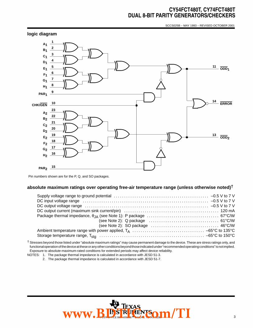
The ’FCT480T devices are high-speed, dual,8-bit parity generators/checkers. Each paritygenerator/checker accepts eight data bits andone parity bit as inputs, and generates a sum andparity-error (ERROR) output. These devices canbe used in odd-parity systems. ERROR is anopen-drain output designed for easy expansion ofthe word width by a wired-OR connection of several ’FCT480T devices. Because no additional logic is needed,the parity-generation or parity-checking times remain the same as for an individual ’FCT480T device.
These devices are fully specified for partial-power-down applications using Ioff. The Ioff circuitry disables theoutputs, preventing damaging current backflow through the device when it is powered down.
Copyright 2001, Texas Instruments IncorporatedPRODUCTION DATA information is current as of publication date.Products conform to specifications per the terms of Texas Instrumentsstandard warranty. Production processing does not necessarily includetesting of all parameters.
Please be aware that an important notice concerning availability, standard warranty, and use in critical applications ofTexas Instruments semiconductor products and disclaimers thereto appears at the end of this data sheet.
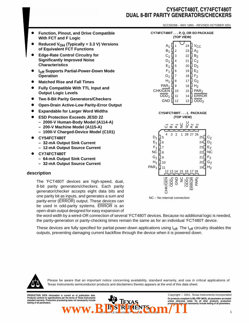
CY54FCT480T . . . L PACKAGE(TOP VIEW)
CY74FCT480T . . . P, Q, OR SO PACKAGE(TOP VIEW)
A1B1C1D1E1F1G1H1
PAR1CHK/GEN
ODD1GND
VCCA2B2C2D2E2F2G2H2PAR2ERRORODD2
1
2
3
4
5
6
7
8
9
10
11
12
24
23
22
21
20
19
18
17
16
15
14
13
3 2 1
13 14
5
6
7
8
9
10
11
C2D2E2NCF2G2H2
D1E1F1
NCG1H1
PAR1
4
15 16 17 18
GN
DN
C
ER
RO
RP
AR
C NC
28 27 2625
24
23
22
21
20
1912
CH
K/G
EN
CC
V
NC – No internal connection2
OD
D2
OD
D1
1B
1A
1
A2
B2
On products compliant to MIL-PRF-38535, all parameters are testedunless otherwise noted. On all other products, productionprocessing does not necessarily include testing of all parameters.www.BDTIC.com/TI
† Stresses beyond those listed under “absolute maximum ratings” may cause permanent damage to the device. These are stress ratings only, andfunctional operation of the device at these or any other conditions beyond those indicated under “recommended operating conditions” is not implied.Exposure to absolute-maximum-rated conditions for extended periods may affect device reliability.
NOTES: 1. The package thermal impedance is calculated in accordance with JESD 51-3.2. The package thermal impedance is calculated in accordance with JESD 51-7.
∆ICCVCC = 5.5 V, VIN = 3.4 V§, f1 = 0, Outputs open 0.5 2
mA∆ICCVCC = 5.25 V, VIN = 3.4 V§, f1 = 0, Outputs open 0.5 2
mA
† Typical values are at VCC = 5 V, TA = 25°C.‡ Not more than one output should be shorted at a time. Duration of short should not exceed one second. The use of high-speed test apparatus and/or
sample-and-hold techniques are preferable to minimize internal chip heating and more accurately reflect operational values. Otherwise, prolongedshorting of a high output can raise the chip temperature well above normal and cause invalid readings in other parametric tests. In any sequenceof parameter tests, IOS tests should be performed last.
§ Per TTL-driven input (VIN = 3.4 V); all other inputs at VCC or GND
electrical characteristics over recommended operating free-air temperature range (unlessotherwise noted) (continued)
PARAMETER TEST CONDITIONSCY54FCT480T CY74FCT480T
UNITPARAMETER TEST CONDITIONSMIN TYP† MAX MIN TYP† MAX
UNIT
ICCD¶
VCC = 5.5 V, Outputs open,One bit switching at 50% duty cycle,VIN ≤ 0.2 V or VIN ≥ VCC – 0.2 V
0.06 0.12
mA/ICCD¶
VCC = 5.25 V, Outputs open,One bit switching at 50% duty cycle,VIN ≤ 0.2 V or VIN ≥ VCC – 0.2 V
0.06 0.12
MHz
#
One bitswitching at f1 = 2.5 MHz
VIN ≤ 0.2 V orVIN ≥ VCC – 0.2 V
0.7 1.4
#
VCC = 5.5 V,f0 0 MHz
1at 50% dutycycle VIN = 3.4 V or GND 1 2.4
#
f0 = 0 MHz,Outputs open 16 bits
switching at f1 = 2.5 MHz
VIN ≤ 0.2 V orVIN ≥ VCC – 0.2 V
2.5 5||
IC#
1at 50% dutycycle VIN = 3.4 V or GND 6.5 21||
mAIC#One bitswitching at f1 = 2.5 MHz
VIN ≤ 0.2 V orVIN ≥ VCC – 0.2 V
0.7 1.4
mA
VCC = 5.25 V,f0 0 MHz
1at 50% dutycycle VIN = 3.4 V or GND 1 2.4
f0 = 0 MHz,Outputs open 16 bits
switching at f1 = 2.5 MHz
VIN ≤ 0.2 V orVIN ≥ VCC – 0.2 V
2.5 5||
1at 50% dutycycle VIN = 3.4 V or GND 6.5 21||
Ci 5 10 5 10 pF
Co 9 12 9 12 pF
† Typical values are at VCC = 5 V, TA = 25°C.¶ This parameter is derived for use in total power-supply calculations.# IC= ICC + ∆ICC × DH × NT + ICCD (f0/2 + f1 × N1)
Where:IC= Total supply currentICC= Power-supply current with CMOS input levels∆ICC= Power-supply current for a TTL high input (VIN = 3.4 V)DH= Duty cycle for TTL inputs highNT= Number of TTL inputs at DHICCD= Dynamic current caused by an input transition pair (HLH or LHL)f0= Clock frequency for registered devices, otherwise zerof1= Input signal frequencyN1= Number of inputs changing at f1All currents are in milliamperes and all frequencies are in megahertz.
|| Values for these conditions are examples of the ICC formula.
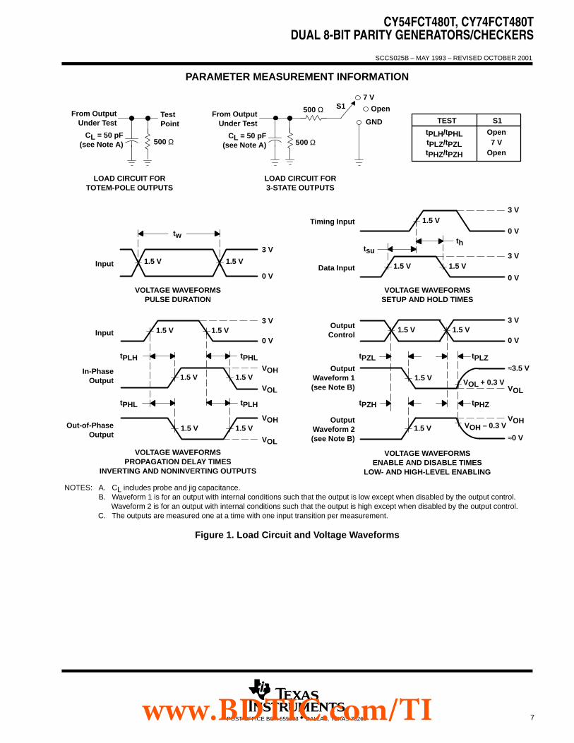
NOTES: A. CL includes probe and jig capacitance.B. Waveform 1 is for an output with internal conditions such that the output is low except when disabled by the output control.
Waveform 2 is for an output with internal conditions such that the output is high except when disabled by the output control.C. The outputs are measured one at a time with one input transition per measurement.
NOTES: A. CL includes probe and jig capacitance.B. All input pulses are supplied by generators having the following characteristics: PRR ≤ 1 MHz, ZO = 50 Ω, tr ≤ 3 ns, tf ≤ 3 ns.C. The outputs are measured one at a time with one input transition per measurement.
From OutputUnder Test
CL(see Note A)
TestPoint
LOAD CIRCUIT FOROPEN-DRAIN OUTPUTS
1.5 V 1.5 V500 Ω
Output
7 V
VOL
≈VCC1.5 V VOL + 0.3 V
500 Ω
Figure 2. Load Circuit and Voltage Waveforms
www.BDTIC.com/TI
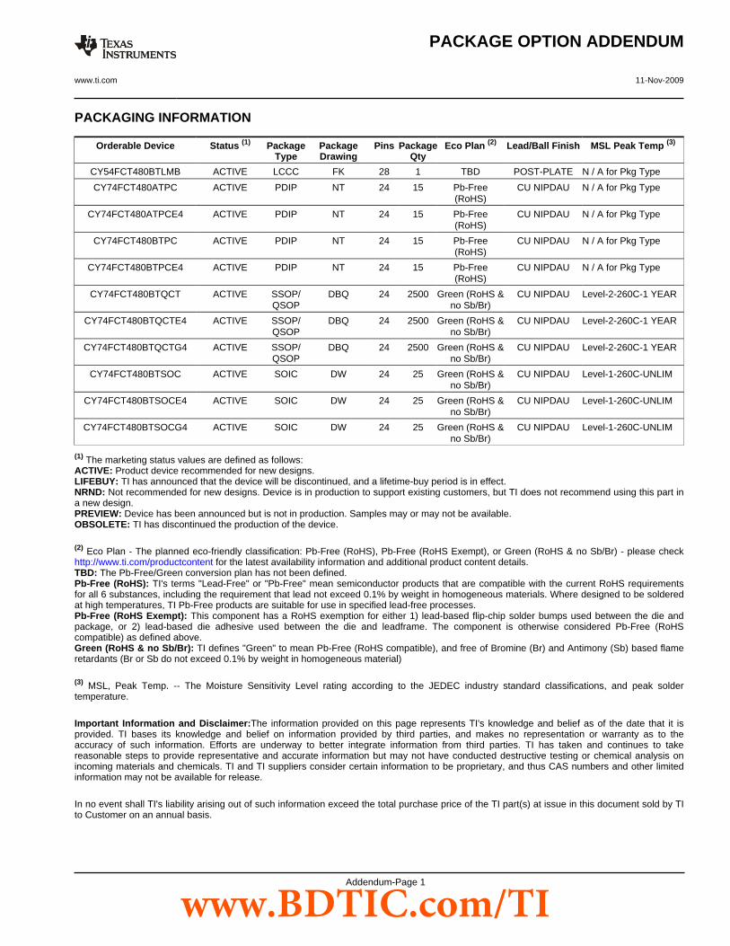
PACKAGING INFORMATION
Orderable Device Status (1) PackageType
PackageDrawing
Pins PackageQty
Eco Plan (2) Lead/Ball Finish MSL Peak Temp (3)
CY54FCT480BTLMB ACTIVE LCCC FK 28 1 TBD POST-PLATE N / A for Pkg Type
CY74FCT480ATPC ACTIVE PDIP NT 24 15 Pb-Free(RoHS)
CU NIPDAU N / A for Pkg Type
CY74FCT480ATPCE4 ACTIVE PDIP NT 24 15 Pb-Free(RoHS)
CU NIPDAU N / A for Pkg Type
CY74FCT480BTPC ACTIVE PDIP NT 24 15 Pb-Free(RoHS)
CU NIPDAU N / A for Pkg Type
CY74FCT480BTPCE4 ACTIVE PDIP NT 24 15 Pb-Free(RoHS)
CU NIPDAU N / A for Pkg Type
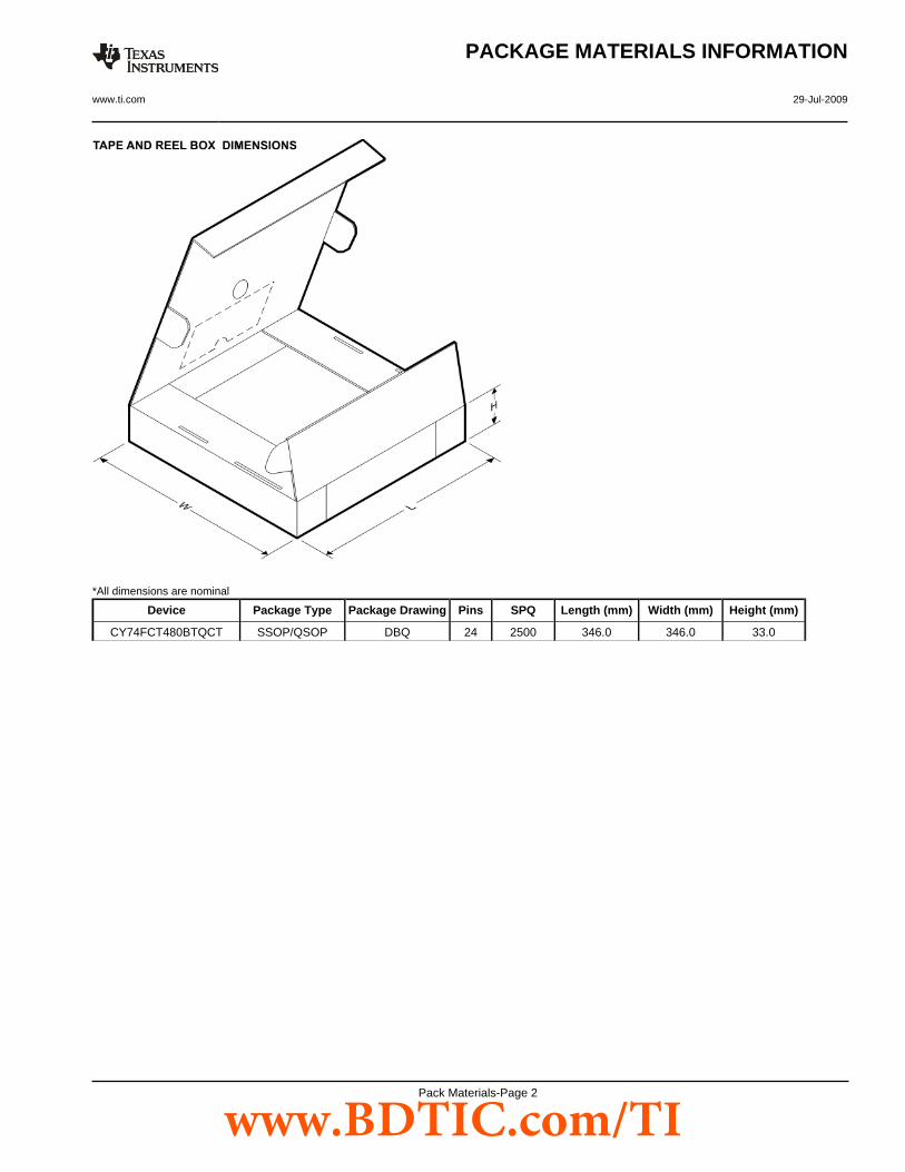
CY74FCT480BTQCT ACTIVE SSOP/QSOP
DBQ 24 2500 Green (RoHS &no Sb/Br)
CU NIPDAU Level-2-260C-1 YEAR
CY74FCT480BTQCTE4 ACTIVE SSOP/QSOP
DBQ 24 2500 Green (RoHS &no Sb/Br)
CU NIPDAU Level-2-260C-1 YEAR
CY74FCT480BTQCTG4 ACTIVE SSOP/QSOP
DBQ 24 2500 Green (RoHS &no Sb/Br)
CU NIPDAU Level-2-260C-1 YEAR
CY74FCT480BTSOC ACTIVE SOIC DW 24 25 Green (RoHS &no Sb/Br)
CU NIPDAU Level-1-260C-UNLIM
CY74FCT480BTSOCE4 ACTIVE SOIC DW 24 25 Green (RoHS &no Sb/Br)
CU NIPDAU Level-1-260C-UNLIM
CY74FCT480BTSOCG4 ACTIVE SOIC DW 24 25 Green (RoHS &no Sb/Br)
CU NIPDAU Level-1-260C-UNLIM
(1) The marketing status values are defined as follows:ACTIVE: Product device recommended for new designs.LIFEBUY: TI has announced that the device will be discontinued, and a lifetime-buy period is in effect.NRND: Not recommended for new designs. Device is in production to support existing customers, but TI does not recommend using this part ina new design.PREVIEW: Device has been announced but is not in production. Samples may or may not be available.OBSOLETE: TI has discontinued the production of the device.
(2) Eco Plan - The planned eco-friendly classification: Pb-Free (RoHS), Pb-Free (RoHS Exempt), or Green (RoHS & no Sb/Br) - please checkhttp://www.ti.com/productcontent for the latest availability information and additional product content details.TBD: The Pb-Free/Green conversion plan has not been defined.Pb-Free (RoHS): TI's terms "Lead-Free" or "Pb-Free" mean semiconductor products that are compatible with the current RoHS requirementsfor all 6 substances, including the requirement that lead not exceed 0.1% by weight in homogeneous materials. Where designed to be solderedat high temperatures, TI Pb-Free products are suitable for use in specified lead-free processes.Pb-Free (RoHS Exempt): This component has a RoHS exemption for either 1) lead-based flip-chip solder bumps used between the die andpackage, or 2) lead-based die adhesive used between the die and leadframe. The component is otherwise considered Pb-Free (RoHScompatible) as defined above.Green (RoHS & no Sb/Br): TI defines "Green" to mean Pb-Free (RoHS compatible), and free of Bromine (Br) and Antimony (Sb) based flameretardants (Br or Sb do not exceed 0.1% by weight in homogeneous material)
(3) MSL, Peak Temp. -- The Moisture Sensitivity Level rating according to the JEDEC industry standard classifications, and peak soldertemperature.
Important Information and Disclaimer:The information provided on this page represents TI's knowledge and belief as of the date that it isprovided. TI bases its knowledge and belief on information provided by third parties, and makes no representation or warranty as to theaccuracy of such information. Efforts are underway to better integrate information from third parties. TI has taken and continues to takereasonable steps to provide representative and accurate information but may not have conducted destructive testing or chemical analysis onincoming materials and chemicals. TI and TI suppliers consider certain information to be proprietary, and thus CAS numbers and other limitedinformation may not be available for release.
In no event shall TI's liability arising out of such information exceed the total purchase price of the TI part(s) at issue in this document sold by TIto Customer on an annual basis.
IMPORTANT NOTICETexas Instruments Incorporated and its subsidiaries (TI) reserve the right to make corrections, modifications, enhancements, improvements,and other changes to its products and services at any time and to discontinue any product or service without notice. Customers shouldobtain the latest relevant information before placing orders and should verify that such information is current and complete. All products aresold subject to TI’s terms and conditions of sale supplied at the time of order acknowledgment.TI warrants performance of its hardware products to the specifications applicable at the time of sale in accordance with TI’s standardwarranty. Testing and other quality control techniques are used to the extent TI deems necessary to support this warranty. Except wheremandated by government requirements, testing of all parameters of each product is not necessarily performed.TI assumes no liability for applications assistance or customer product design. Customers are responsible for their products andapplications using TI components. To minimize the risks associated with customer products and applications, customers should provideadequate design and operating safeguards.TI does not warrant or represent that any license, either express or implied, is granted under any TI patent right, copyright, mask work right,or other TI intellectual property right relating to any combination, machine, or process in which TI products or services are used. Informationpublished by TI regarding third-party products or services does not constitute a license from TI to use such products or services or awarranty or endorsement thereof. Use of such information may require a license from a third party under the patents or other intellectualproperty of the third party, or a license from TI under the patents or other intellectual property of TI.Reproduction of TI information in TI data books or data sheets is permissible only if reproduction is without alteration and is accompaniedby all associated warranties, conditions, limitations, and notices. Reproduction of this information with alteration is an unfair and deceptivebusiness practice. TI is not responsible or liable for such altered documentation. Information of third parties may be subject to additionalrestrictions.Resale of TI products or services with statements different from or beyond the parameters stated by TI for that product or service voids allexpress and any implied warranties for the associated TI product or service and is an unfair and deceptive business practice. TI is notresponsible or liable for any such statements.TI products are not authorized for use in safety-critical applications (such as life support) where a failure of the TI product would reasonablybe expected to cause severe personal injury or death, unless officers of the parties have executed an agreement specifically governingsuch use. Buyers represent that they have all necessary expertise in the safety and regulatory ramifications of their applications, andacknowledge and agree that they are solely responsible for all legal, regulatory and safety-related requirements concerning their productsand any use of TI products in such safety-critical applications, notwithstanding any applications-related information or support that may beprovided by TI. Further, Buyers must fully indemnify TI and its representatives against any damages arising out of the use of TI products insuch safety-critical applications.TI products are neither designed nor intended for use in military/aerospace applications or environments unless the TI products arespecifically designated by TI as military-grade or "enhanced plastic." Only products designated by TI as military-grade meet militaryspecifications. Buyers acknowledge and agree that any such use of TI products which TI has not designated as military-grade is solely atthe Buyer's risk, and that they are solely responsible for compliance with all legal and regulatory requirements in connection with such use.TI products are neither designed nor intended for use in automotive applications or environments unless the specific TI products aredesignated by TI as compliant with ISO/TS 16949 requirements. Buyers acknowledge and agree that, if they use any non-designatedproducts in automotive applications, TI will not be responsible for any failure to meet such requirements.Following are URLs where you can obtain information on other Texas Instruments products and application solutions:Products ApplicationsAmplifiers amplifier.ti.com Audio www.ti.com/audioData Converters dataconverter.ti.com Automotive www.ti.com/automotiveDLP® Products www.dlp.com Broadband www.ti.com/broadbandDSP dsp.ti.com Digital Control www.ti.com/digitalcontrolClocks and Timers www.ti.com/clocks Medical www.ti.com/medicalInterface interface.ti.com Military www.ti.com/militaryLogic logic.ti.com Optical Networking www.ti.com/opticalnetworkPower Mgmt power.ti.com Security www.ti.com/securityMicrocontrollers microcontroller.ti.com Telephony www.ti.com/telephonyRFID www.ti-rfid.com Video & Imaging www.ti.com/videoRF/IF and ZigBee® Solutions www.ti.com/lprf Wireless www.ti.com/wireless