86
ECE 451 – Jose Schutt‐Aine 1 ECE 451 Advanced Microwave Measurements Signal Integrity Jose E. Schutt-Aine Electrical & Computer Engineering University of Illinois [email protected]
| Date post: | 26-Jul-2018 |
| Category: |
Documents |
| Upload: | nguyendiep |
| View: | 218 times |
| Download: | 0 times |

ECE 451 – Jose Schutt‐Aine 1
ECE 451Advanced Microwave Measurements
Signal Integrity
Jose E. Schutt-AineElectrical & Computer Engineering
University of [email protected]

ECE 451 – Jose Schutt‐Aine 2
• Attenuation & Loss (skin effect, on-chip loss)• Crosstalk (interconnect proximity, coupling)• Dispersion (frequency dependence of parameters)• Reflection (unmatched loads, reactive loads, ISI)• Distortion (nonlinear loads)• Interference & Radiation (EMI/EMC)• Rise time degradation• Clock skew (different electrical path lengths)
Signal Integrity

ECE 451 – Jose Schutt‐Aine 3
PCI
• PC InterfaceFor external cardsGraphics, Network, Sound, etc…Parallel

ECE 451 – Jose Schutt‐Aine 4
• Computer Expansion Card StandardReplaced older PCIBased on serial linksCapacity up to 1 Gb/sV3.0 scheduled for 2010
PCI‐Express

ECE 451 – Jose Schutt‐Aine 5
Universal Serial Bus (USB)
• Interfaces devices to computersNo rebootingLow powerNo need for external power supply480 Mb/s

ECE 451 – Jose Schutt‐Aine 66
• Expansion Card StandardReplaced older PCIBased on serial linksCapacity up to 1 Gb/sV3.0 scheduled for 2010
IDE
ECE 451 – Jose Schutt‐Aine 7
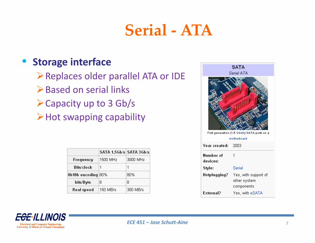
Serial ‐ ATA
• Storage interfaceReplaces older parallel ATA or IDEBased on serial linksCapacity up to 3 Gb/sHot swapping capability

ECE 451 – Jose Schutt‐Aine 88
Motherboards and Backplanes

ECE 451 – Jose Schutt‐Aine 9
Cables and Transmission Lines
coaxial
twisted pairs

ECE 451 – Jose Schutt‐Aine 10
Cable Specifications

ECE 451 – Jose Schutt‐Aine 11
Computer Interconnections

ECE 451 – Jose Schutt‐Aine 12
Chip size(mm2)
Number of transistors(million)
Interconnect width(nm)
Total interconnect length(km)
1997 2003 20122006
300 430 750520
11 76 200 1400
200 100 70 35
2.16 2.84 5.14 24
Semiconductor Technology Trends

ECE 451 – Jose Schutt‐Aine 13
Source: M. Bohr and Y. El-Mansy - IEEE TED Vol. 4, March 1998
5‐Layer Interconnect Technology 0.25 m
Vertical parallel-plate capacitance 0.05 fF/m2
Vertical parallel-plate capacitance (min width) 0.03 fF/mVertical fringing capacitance (each side) 0.01 fF/mHorizontal coupling capacitance (each side) 0.03

ECE 451 – Jose Schutt‐Aine 14
Metal 5
Metal 4
Metal 3Metal 2
Metal 1
Substrate
Vertical parallel-plate capacitance 0.05 fF/m2
Vertical parallel-plate capacitance (min width) 0.03 fF/mVertical fringing capacitance (each side) 0.01 fF/mHorizontal coupling capacitance (each side) 0.03
Integrated Circuit Wiring

ECE 451 – Jose Schutt‐Aine 15
Source: ITRS roadmap 2004
Signal Delay Trend
Signal Delay
Delay for Metal 1 and Global Wiring versus Feature Size
gates delay
interconnect delayGlobal
Wiring w/o Repeaters
GlobalWiring w
Repeaters
LocalWiring
Gate Delay

ECE 451 – Jose Schutt‐Aine 16
0
5
10
15
20
25
Del
ay (p
s)
30
35
40
45
650 595 540 485Generation (nm)
SPEED/PERFORMANCE ISSUE
Gate Delay
Sum of Delays, Al & SiO2
Sum of Delays, Cu & Low K
Interconnect Delay, Al & SiO2
Interconnect Delay, Cu & Low K
430 375 320 265 210 155 100
Gate wi Al & SiO2
Gate
Al 3.0 -cmCu 1.7 -cmSiO2 = 4.0Low = 2.0Al & Cu .8 ThickAl & Cu Line 43 Long
The Interconnect Bottleneck

ECE 451 – Jose Schutt‐Aine 17
• Total interconnect length (m/cm2) – active wiring only, excluding global levels will increases:
• Interconnect power dissipation is more than 50% of the total dynamic power consumption in 130nm and will become dominant in future technology nodes
• Interconnect centric design flows have been adopted to reduce the length of the critical signal path
Interconnect
Year 2003 2004 2005 2006 2007 2008 2009Total
Length 579 688 907 1002 1117 1401 1559
ECE 451 – Jose Schutt‐Aine 18
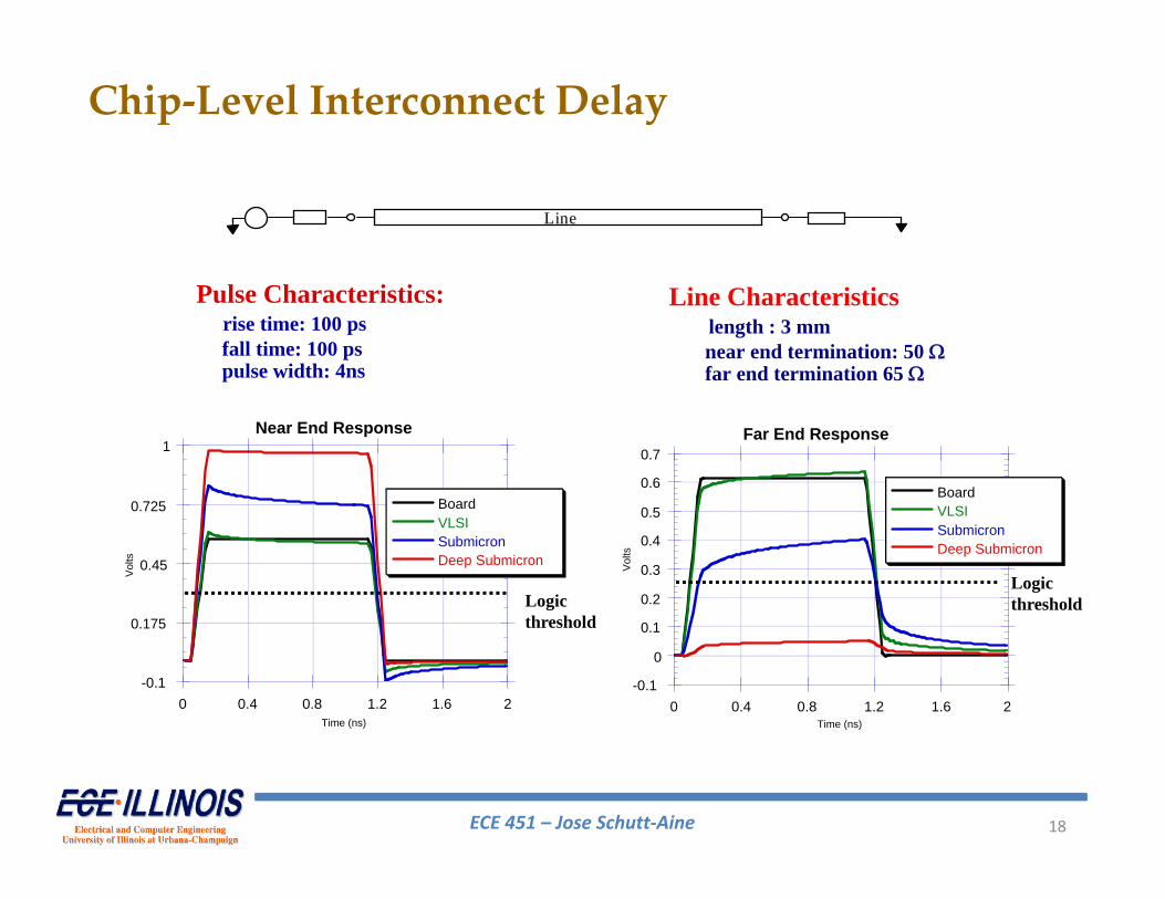
Chip‐Level Interconnect Delay
Line
-0.1
0
0.1
0.2
0.3
0.4
0.5
0.6
0.7
Vol
ts
0 0.4 0.8 1.2 1.6 2Time (ns)
Far End Response
BoardVLSISubmicronDeep Submicron
-0.1
0.175
0.45
0.725
1
0 0.4
Vol
ts
0.8 1.2 1.6 2Time (ns)
Near End Response
BoardVLSISubmicronDeep Submicron
Pulse Characteristics: rise time: 100 ps fall time: 100 ps pulse width: 4ns
Line Characteristics length : 3 mm near end termination: 50 far end termination 65
LogicthresholdLogic
threshold

ECE 451 – Jose Schutt‐Aine 19
Package‐Level Complexity
- Up to 16 layers- Hundreds of vias- Thousands of TLs- High density- Nonuniformity

ECE 451 – Jose Schutt‐Aine 20
TransmissionChannel
TransmissionChannel
TransmissionChannel
Ideal
Common
Noisy
Signal Integrity
ECE 451 – Jose Schutt‐Aine 21
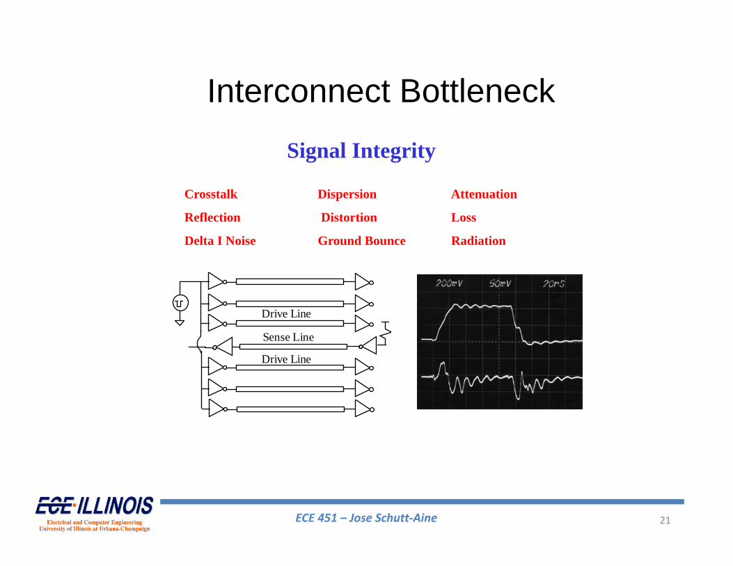
Signal Integrity
Crosstalk Dispersion Attenuation
Reflection Distortion Loss
Delta I Noise Ground Bounce Radiation
Sense Line
Drive Line
Drive Line
Interconnect Bottleneck

ECE 451 – Jose Schutt‐Aine 22
Reflection in Transmission Lines
1.
2.
3.

ECE 451 – Jose Schutt‐Aine 23
Metallic Conductors
Length
Area
Re sist an ce : R
Package level:W=3 milsR=0.0045 /mm
R = Le ng th Are a
Submicron level:W=0.25 micronsR=422 /mm

ECE 451 – Jose Schutt‐Aine 24
Metal Conductivity -1 m 10-7)
Silver 6.1Copper 5.8Gold 3.5Aluminum 1.8Tungsten 1.8Brass 1.5Solder 0.7Lead 0.5Mercury 0.1
Metallic Conductors

ECE 451 – Jose Schutt‐Aine 25
RF SOURCE
Loss in Transmission Lines

ECE 451 – Jose Schutt‐Aine 26
Low Frequency High Frequency Very High Frequency
Skin Effect in Transmission Lines

ECE 451 – Jose Schutt‐Aine 27
Skin Depth
1
The decay of electromagnetic wave propagating into a conductor is measured in terms of the skin depth
2
For good conductors:
ˆ ˆz z j zo oE xE e xE e e
Wave decay
Definition: skin depth is distance over which amplitude of wave drops by 1/e.

ECE 451 – Jose Schutt‐Aine 28
Skin Depth
I VCz t
e-1Wave motion
For perfect conductor, = 0 and current only flows on the surface

ECE 451 – Jose Schutt‐Aine 29
DC Resistance
dclRwt
l: conductor length: conductivity

ECE 451 – Jose Schutt‐Aine 30
AC Resistance
2 /acl l l fRw ww
l: conductor length: conductivityf: frequency
ECE 451 – Jose Schutt‐Aine 31
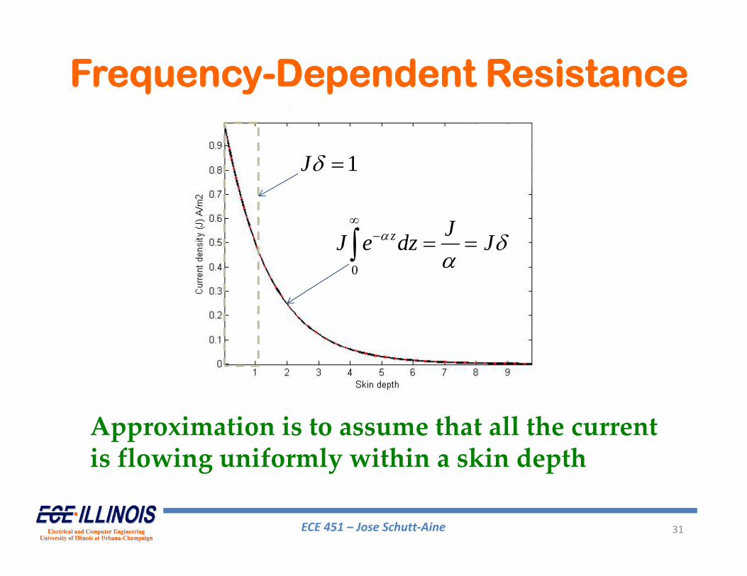
Frequency-Dependent Resistance
1J
0
z JJ e dz J
Approximation is to assume that all the current is flowing uniformly within a skin depth
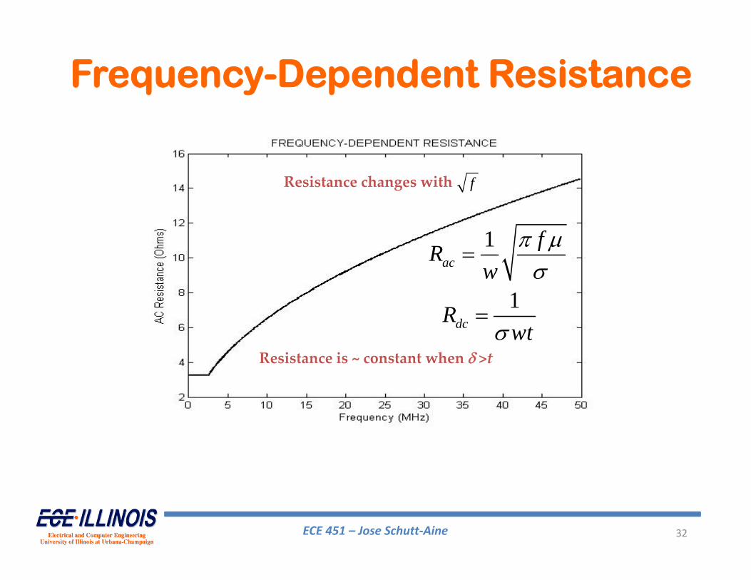
ECE 451 – Jose Schutt‐Aine 32
2 2
2 2
I ICLz t
1
acfR
w
1dcR
wt
Resistance is ~ constant when >t
Resistance changes with f
Frequency-Dependent Resistance

ECE 451 – Jose Schutt‐Aine 33
, 6ac groundl fRh
Reference Plane Current

ECE 451 – Jose Schutt‐Aine 34
r
H. A. Wheeler, "Formulas for the skin effect," Proc. IRE, vol. 30, pp. 412-424,1942
Skin Effect in Microstrip

ECE 451 – Jose Schutt‐Aine 35
/ /y jyoJ J e e
/ /
0 1y jy o
oJ wI J we e dy
j
oo o o
JE J E
oo
J DV E D
Current density varies as
Note that the phase of the current density varies as a function of y
The voltage measured over a section of conductor of length D is:
Skin Effect in Microstrip

ECE 451 – Jose Schutt‐Aine 36
11o
skino
jJ DV DZ j fI J w w
1
skin skinDR X fw
The skin effect impedance is
where
Skin Effect in Microstrip
is the bulk resistivity of the conductor
skin skin skinZ R jX
with
Skin effect has reactive (inductive) component

ECE 451 – Jose Schutt‐Aine 37
internalac skinR RL
The internal inductance can be calculated directly from the ac resistance
Internal Inductance
Skin effect resistance goes up with frequency
Skin effect inductance goes down with frequency

ECE 451 – Jose Schutt‐Aine 38
When the tooth height is comparable to the skin depth, roughness effects cannot be ignored
Surface Roughness
Copper surfaces are rough to facilitate adhesion to dielectric during PCB manufacturing
Surface roughness will increase ohmic losses

ECE 451 – Jose Schutt‐Aine 39
Vz
= (R+ jL)I = ZI
Iz
= (G+ jC)V = YV
Lossy Transmission LineL
z
C
I
V
+
-
G
R
Telegraphers Equation

ECE 451 – Jose Schutt‐Aine 40
z
R, L, G, C,
Lossy Transmission Line
forward wave
backward wave

ECE 451 – Jose Schutt‐Aine 41
Coupled Lines and Crosstalk
r
w s
h
Cs
V1
V2
I1
I2
Cs
Cm Lm

ECE 451 – Jose Schutt‐Aine 42
50 line 1
line 2
50
line 1
line 2
50 line 1
line 2
line 1
line 2
Crosstalk noise depends on termination

ECE 451 – Jose Schutt‐Aine 43
50 line 1
line 2
50
line 1
line 2
line 1
line 2
tr = 1 ns tr = 7 ns
Crosstalk depends on signal rise time

ECE 451 – Jose Schutt‐Aine 44
tr = 1 ns tr = 7 ns
Crosstalk depends on signal rise time
50 line 1
line 2
line 1
line 2
line 1
line 2

ECE 451 – Jose Schutt‐Aine 45
-0.2
0
0.2
0.4
0.6
0.8
1
Vol
ts
0 5 10 15 20 25 30
Time (ns)
Drive Line at Near End
35 40
-0.15
-0.1
-0.05
0
0.05
0.1
0.15
0.2
Vol
ts
0 5 10 15 20 25 30
Time (ns)
Sense Line at Near End
35 40

ECE 451 – Jose Schutt‐Aine 46
ALS04 ALS240Drive Line 1
Drive Line 2
z=0 z=l
Drive Line 3
Sense Line 4
Drive Line 5
Drive Line 6
Drive Line 7
ALS04
ALS04
ALS04
ALS04
ALS04
ALS240
ALS240
ALS240
ALS240
ALS240
7-Line Coupled-Microstrip System
Ls = 312 nH/m; Cs = 100 pF/m;
Lm = 85 nH/m; Cm = 12 pF/m.

ECE 451 – Jose Schutt‐Aine 47
20010000
1
2
3
4
5Drive line 3 at Near End
Time (ns)2001000
-1
0
1
2
3
4
5Drive Line 3 at Far End
Time (ns)
Drive Line 3

ECE 451 – Jose Schutt‐Aine 48
2001000-1
0
1
2Sense Line at Near End
Time (ns)2001000
-1
0
1
2Sense Line at Far End
Time (ns)
Sense Line

ECE 451 – Jose Schutt‐Aine 49
IC on Package

ECE 451 – Jose Schutt‐Aine 50
Simultaneous switching and inductance (Leff)
Leff is f( current magnitude and direction)
Interactions between noise generated by power/ground and signal paths
Mixed Signal Noise
Power bus
Interconnect
Analog Digital
coupled noise
Substrate
Power bus
Interconnect
GND
bond InductanceChip-packageinterconnect

ECE 451 – Jose Schutt‐Aine 51
- Power-supply-level fluctuations- Delta-I noise- Simultaneous switching noise (SSN)- Ground bounce
IdealVout
ActualVout
VOH
VOL
Time
Power‐Supply Noise

ECE 451 – Jose Schutt‐Aine 52
+
-
Gate A Gate C
RWire B
N
Output voltage fromGate A
+
-
V1
Differential voltageat receiverV1 - R
GROUND CONNECTIONInternalreferencegenerator
+
-
V1
+-
+
-
Gate A Gate C
RWire B
N
Equivalent noisesource in serieswith ground connection
Output voltage fromGate A
+
-
V1
Differential voltageat receiverV2 - N - R
GROUND CONNECTIONInternalreferencegenerator
+
-
V2
Power Distribution Problem
At high frequencies, Wire B is a transmission line and ground connection is no longer the reference voltage
Low Frequency
High Frequency

ECE 451 – Jose Schutt‐Aine 53
VP Bus
VP Bus
VP Bus
VP Bus
VP Bus
GND Bus
GND Bus
GND Bus
GND Bus
VP
GND
Local Buses
Wiring Tracks
• Distribution Network for Peripheral Bonding– Power and ground are brought onto the chip via bond pads located
along the four edges– Metal buses provide routing from the edges to the remainder of the chip
On‐Chip Power and Ground Distribution

ECE 451 – Jose Schutt‐Aine 54
• Signal launched on a transmission line can be affected by previous signals as result of reflections
• ISI can be a major concern especially if the signal delay is smaller than twice the time of flight
• ISI can have devastating effects
• Noise must be allowed to settled before next signal is sent
Intersymbol Interference (ISI)

ECE 451 – Jose Schutt‐Aine 55
Volts
Time
Waveform beginning transition from low to highwith unsettled noise on the bus
Different starting point due to ISI
Receiver switching threshold
Timing differencedue to ISI
Ideal waveform beginning transistionfrom low to high with no noise on the bus
Intersymbol Interference

ECE 451 – Jose Schutt‐Aine 56
• Minimize reflections on the bus by avoiding impedance discontinuities
• Minimize stub lengths and large parasitics from package sockets or connectors
• Keep interconnects as short as possible (minimize delay)
• Minimize crosstalk effects
Minimizing ISI

ECE 451 – Jose Schutt‐Aine 57
Measurements
VNA: S-parameter Spectrum Analyzer
Time-domain simulation Eye diagram

ECE 451 – Jose Schutt‐Aine 58
• Timing uncertainties in digital transmission systems• Utmost importance because timing uncertainties cause bit errors• There are different types of jitter
Jitter Definition
Jitter is difference in time of when somethingwas ideally to occur and when it actually did occur.
Some devices specify the amount of marginal jitter and totaljitter that it can take to operate correctly. If the cable adds more jitter than the receiver’s allowed marginal jitter and total jitter the signal will not be received correctly. In this case the jitter is measured as in the below diagram

ECE 451 – Jose Schutt‐Aine 59
• Jitter is a signal timing deviation referenced to a recovered clock from the recovered bit stream
• Measured in Unit Intervals and captured visually with eye diagrams
• Two types of jitter– Deterministic (non Gaussian)– Random
• The total jitter (TJ) is the sum of the random (RJ) and deterministic jitter(DJ)
Jitter Characteristics

ECE 451 – Jose Schutt‐Aine 60
Types of Jitter
•Deterministic Jitter (DDJ)Data‐Dependent Jitter (DDJ)Periodic Jitter (PJ)Bounded Uncorrelated Jitter (BUJ)
• Random Jitter (RJ)Gaussian Jitter fHigher‐Order Jitter

Bandwidth Limitations Cause intersymbol interference (ISI) ISI occurs if time required by signal to completely charge is longer
than bit interval Amount of ISI is function of channel and data content of signal
Jitter Effects
Oscillator Phase Noise Present in reference clocks or high-speed clocks In PLL based clocks, phase noise can be amplified

ECE 451 – Jose Schutt‐Aine 62
Jitter StatisticsMost common way to look at jitter is in statistical domain
Because one can observe jitter histograms directly on oscilloscopes
No instruments to measure jitter time waveform or frequency spectrum directly
Jitter Histograms and Probability Density Functions (PDF)Built directly from time waveforms Frequency information is lostPeak‐to‐peak value depends on observation time

ECE 451 – Jose Schutt‐Aine 63
Total Jitter Time Waveform
The total jitter waveform is the sum of individual components
TJ(t) = PJ(t) + RJ(t)

ECE 451 – Jose Schutt‐Aine 64
Jitter Statistics
TJ(x) = PJ(x) * RJ(x)
The total jitter PDF is the convolution of individual components

ECE 451 – Jose Schutt‐Aine 65
An eye diagram is a time-folded representation of a signal that carries digital information
Eye Diagram

ECE 451 – Jose Schutt‐Aine 66
Eye Diagram Construction
Eye diagram construction in real-time oscilloscope is based on hardware clock recovery and trigger circuitry

ECE 451 – Jose Schutt‐Aine 67
Eye Diagram Construction

ECE 451 – Jose Schutt‐Aine 68
1. Capture of the Waveform Record
2. Determine the Edge Times
Eye Diagram Construction

ECE 451 – Jose Schutt‐Aine 69
Eye Diagram Construction
3. Determine the Bit Labels

ECE 451 – Jose Schutt‐Aine 70
4. Clock Recovery
Eye Diagram Construction

ECE 451 – Jose Schutt‐Aine 71
Eye Diagram Construction
5. Slice Overlay
6. Display

ECE 451 – Jose Schutt‐Aine 72
Eye Diagram Measurements

ECE 451 – Jose Schutt‐Aine 73
Reference Levels

ECE 451 – Jose Schutt‐Aine 74
Eye HeightEye Height is the measuremnt of the eye height in volts
3 3PTop PTop PBase PBaseEye Height
PTop
PBasePBasePTop
: mean value of eye top
: standard deviation of eye top
: mean value of eye base
: standard deviation of eye base

ECE 451 – Jose Schutt‐Aine 75
Eye WidthEye Width is the measuremnt of the eye width in seconds
2 2 1 13 3TCross TCross TCross TCrossEye Width
1Crossing Percent 100%PCross PBase
PTop PBase
Crossing percent measurement is the eye crossing point expressed as a percentage of the eye height

ECE 451 – Jose Schutt‐Aine 76
Eye Diagram Specifications
PCI Express 2.0 eye diagram specification for full and deemphasized signals

ECE 451 – Jose Schutt‐Aine 77
Margin Testing
Eye diagram with low margin

ECE 451 – Jose Schutt‐Aine 78
Pseudorandomsequencegenerator
Transmitter Receiver
Scope
Trig Vert
Clk
Data
Fiber
Eye Pattern Analysis

Typical Eye Diagrams
Eye Diagram

ECE 451 – Jose Schutt‐Aine 80
Eye Diagram ‐ ADS Simulation

ECE 451 – Jose Schutt‐Aine 81
Eye Diagram ‐ ADS SimulationIdeal Matched Line

ECE 451 – Jose Schutt‐Aine 82
Eye Diagram ‐ ADS Simulation5 GHz Data Transmission

ECE 451 – Jose Schutt‐Aine 83
Eye Diagram ‐ ADS Simulation5 GHz Data Transmission

ECE 451 – Jose Schutt‐Aine 84
Eye Diagram ‐ ADS Simulation10 GHz Data Transmission

ECE 451 – Jose Schutt‐Aine 85
Eye Diagram ‐ ADS Simulation

ECE 451 – Jose Schutt‐Aine 86
• The Bit-error rate (BER) quantifies the likelihood of a bit being interpreted at the receiver incorrectly due to jitter- or amplitude-induced degradation on the received signal
• No higher than a 10-16 BER is tolerable no more than 1 error out of 1016 bits.
• BER can be measured directly or quantified with statistical calculations
• Deterministic jitter(DJ) can be easily measured via S-parameters obtained in the frequency domain
Bit‐Error Rate


