ECE 4670 Spring 2014 Lab 1 Linear System Characteristics 1 Linear System Characteristics The first part of this experiment will serve as an introduction to the use of the spectrum analyzer in making absolute amplitude measurements. The signals considered will be common periodic signals which are produced by a function generator (i.e. sine, square, and triangle waveforms). Next swept frequency measurements using a spectrum analyzer with a tracking generator will be investigated. The amplitude response of an active notch will be characterized. In the third portion of this experiment both the amplitude and phase response of linear systems will be considered. The use of a gain-phase meter will be introduced. 1.1 Basic Spectrum Analyzer Measurements The spectrum analyzer is a device which displays an amplitude versus frequency plot of the fre- quency components or spectrum of any input signal. Located on roll-about carts, the lab has three Agilent 4395A spectrum/network analyzers. The analyzers cover the frequency range from 10Hz to 500MHz. The 1 Mhigh impedance adapter, used frequently throughout the course, addition- ally limits the bandwidth to 5 Hz to 100 MHz. The operation of the 4395A is not as difficult as it might appear from just looking at the front panel controls. You will need to spend some time becoming familiar with both the Network Ana- lyzer (quick start guide pp. 3-1 to 3-14) and Spectrum Analyzer (quick start guide pp. 3-15 to 3-30) operating modes. Read through the Quick Start instructions carefully before proceeding any fur- ther with this experiment. For the first part of this experiment you will be using the analyzer in the Spectrum mode. When making measurements with this instrument the first step is to configure the operating state to the proper measurement mode, activate appropriate source and receiver ports, select frequency sweep parameters, and display formats. If you encounter difficulty or become frustrated trying to figure out the front panel controls, please ask the lab instructor for assistance. The detailed front panel operation of both of these analyzers is described in the respective op- erators manual. A PDF version of the 4395A operators manual can be found on the course Web site ( ). Printed copies of the manuals can also be found on the respective carts. Ask your lab instructor to explain anything you don’t understand. The spectrum/network analyzer is a sophisticated instrument and can be easily damaged. DO NOT EXCEED THE MAXIMUM ALLOWABLE INPUT SIGNAL LEVELS (orange lettering be- low the input terminals). This instrument is very expensive, costing in excess of $28,000 when new. Additionally, Agilent no longer makes an instrument with the combined spectrum vector network analysis capability of this instrument, with these same features. Getting a return on our investment is important. An overview of the spectrum analyzer measurement capabilities and input signal level maxi- mums can be found in Table 1. An overview of the network analyzer measurement capabilities and input signal level maximums can be found in Table 2. The spectrum/network analyzer will first be used in the spectrum analyzer mode. Use of the
Transcript
ECE 4670 Spring 2014 Lab 1Linear System Characteristics
1 Linear System CharacteristicsThe first part of this experiment will serve as an introduction to the use of the spectrum analyzerin making absolute amplitude measurements. The signals considered will be common periodicsignals which are produced by a function generator (i.e. sine, square, and triangle waveforms).Next swept frequency measurements using a spectrum analyzer with a tracking generator will beinvestigated. The amplitude response of an active notch will be characterized. In the third portionof this experiment both the amplitude and phase response of linear systems will be considered.The use of a gain-phase meter will be introduced.
1.1 Basic Spectrum Analyzer MeasurementsThe spectrum analyzer is a device which displays an amplitude versus frequency plot of the fre-quency components or spectrum of any input signal. Located on roll-about carts, the lab has threeAgilent 4395A spectrum/network analyzers. The analyzers cover the frequency range from 10Hzto 500MHz. The 1 M� high impedance adapter, used frequently throughout the course, addition-ally limits the bandwidth to 5 Hz to 100 MHz.
The operation of the 4395A is not as difficult as it might appear from just looking at the frontpanel controls. You will need to spend some time becoming familiar with both the Network Ana-lyzer (quick start guide pp. 3-1 to 3-14) and Spectrum Analyzer (quick start guide pp. 3-15 to 3-30)operating modes. Read through the Quick Start instructions carefully before proceeding any fur-ther with this experiment. For the first part of this experiment you will be using the analyzer in theSpectrum mode. When making measurements with this instrument the first step is to configure theoperating state to the proper measurement mode, activate appropriate source and receiver ports,select frequency sweep parameters, and display formats. If you encounter difficulty or becomefrustrated trying to figure out the front panel controls, please ask the lab instructor for assistance.
The detailed front panel operation of both of these analyzers is described in the respective op-erators manual. A PDF version of the 4395A operators manual can be found on the course Website (http://www.eas.uccs.edu/wickert/ece4670). Printed copies of the manuals can alsobe found on the respective carts. Ask your lab instructor to explain anything you don’t understand.The spectrum/network analyzer is a sophisticated instrument and can be easily damaged. DO NOTEXCEED THE MAXIMUM ALLOWABLE INPUT SIGNAL LEVELS (orange lettering be-low the input terminals). This instrument is very expensive, costing in excess of $28,000 whennew. Additionally, Agilent no longer makes an instrument with the combined spectrum vectornetwork analysis capability of this instrument, with these same features. Getting a return on ourinvestment is important.
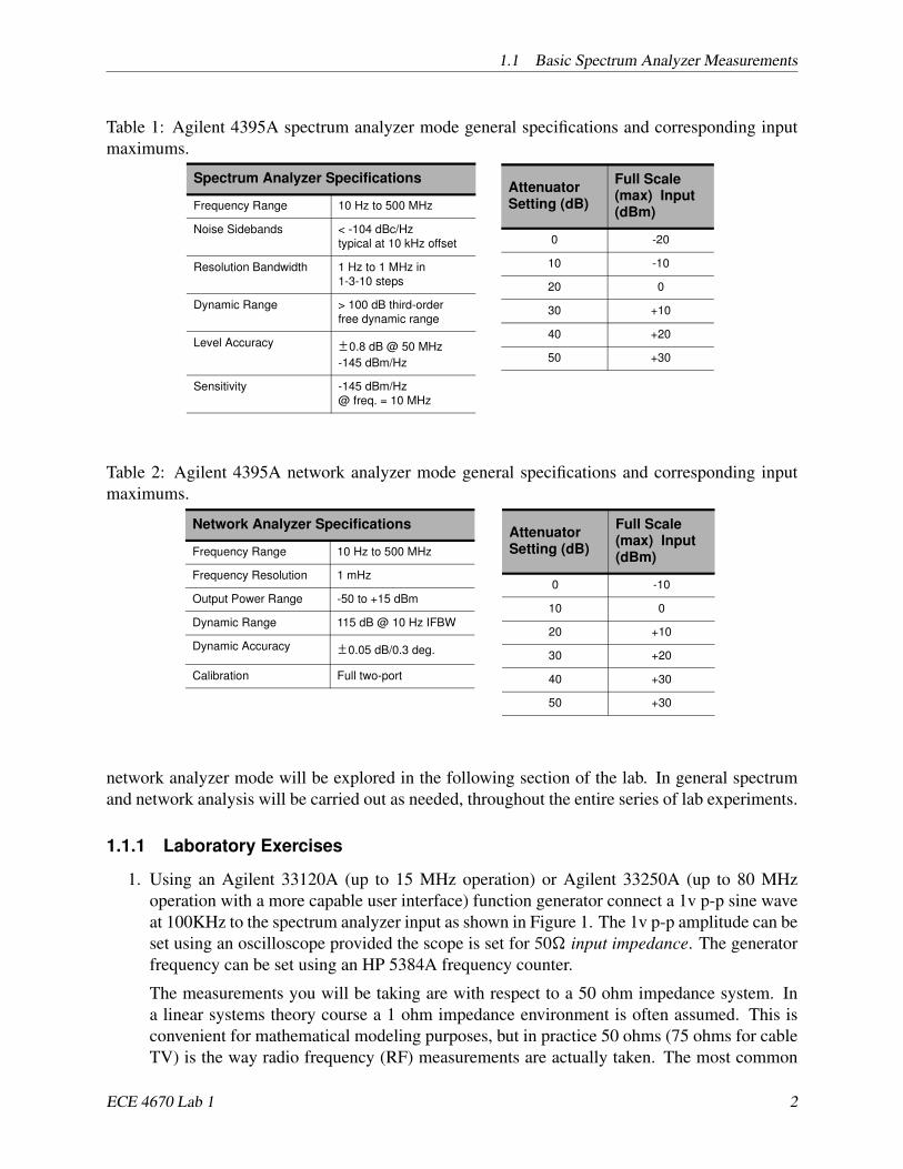
An overview of the spectrum analyzer measurement capabilities and input signal level maxi-mums can be found in Table 1. An overview of the network analyzer measurement capabilities andinput signal level maximums can be found in Table 2.
The spectrum/network analyzer will first be used in the spectrum analyzer mode. Use of the
1.1 Basic Spectrum Analyzer Measurements
Table 1: Agilent 4395A spectrum analyzer mode general specifications and corresponding inputmaximums.
Spectrum Analyzer Specifications
Frequency Range 10 Hz to 500 MHz
Noise Sidebands < -104 dBc/Hz
typical at 10 kHz offset
Resolution Bandwidth 1 Hz to 1 MHz in
1-3-10 steps
Dynamic Range > 100 dB third-order
free dynamic range
Level Accuracy 0.8 dB @ 50 MHz
-145 dBm/Hz
Sensitivity -145 dBm/Hz
@ freq. = 10 MHz
±
Attenuator Setting (dB)
Full Scale (max) Input (dBm)
0 -20
10 -10
20 0
30 +10
40 +20
50 +30
Table 2: Agilent 4395A network analyzer mode general specifications and corresponding inputmaximums.
Network Analyzer Specifications
Frequency Range 10 Hz to 500 MHz
Frequency Resolution 1 mHz
Output Power Range -50 to +15 dBm
Dynamic Range 115 dB @ 10 Hz IFBW
Dynamic Accuracy 0.05 dB/0.3 deg.
Calibration Full two-port
±
Attenuator Setting (dB)
Full Scale (max) Input (dBm)
0 -10
10 0
20 +10
30 +20
40 +30
50 +30
network analyzer mode will be explored in the following section of the lab. In general spectrumand network analysis will be carried out as needed, throughout the entire series of lab experiments.
1.1.1 Laboratory Exercises
1. Using an Agilent 33120A (up to 15 MHz operation) or Agilent 33250A (up to 80 MHzoperation with a more capable user interface) function generator connect a 1v p-p sine waveat 100KHz to the spectrum analyzer input as shown in Figure 1. The 1v p-p amplitude can beset using an oscilloscope provided the scope is set for 50� input impedance. The generatorfrequency can be set using an HP 5384A frequency counter.
The measurements you will be taking are with respect to a 50 ohm impedance system. Ina linear systems theory course a 1 ohm impedance environment is often assumed. This isconvenient for mathematical modeling purposes, but in practice 50 ohms (75 ohms for cableTV) is the way radio frequency (RF) measurements are actually taken. The most common
ECE 4670 Lab 1 2
1.1 Basic Spectrum Analyzer Measurements
Agilent 4395A
0 1 . . . .RF OutLine R BA
Agilent 33250A
Output
100.000 kHz
Verify amplitude andfrequency using a scope and frequencycounter; keep scope
The R, A, or Binput ports may be used
50Ω
impedance level at 1MΩ50Ω
Figure 1: Agilent 4395A Spectrum measurement test setup
display mode for a spectrum analyzer is power in dB relative to one milliwatt (dBm). Theunits are denoted dBm. To find the power in dBm delivered to a 50 ohm load ,from a singlesinusoid waveform, we might start with a scope waveform reading of volts peak-to-peak orpeak. From basic circuit theory, the power delivered to a load R is
Pl D1
2�v2
peak
RD1
2�.vpp=2/
2
RDv2
rms
Rwatts: (1)
Recall that for a sinusoid, the rms value is vpeak=p2, and clearly the peak value is one half
the peak-to-peak value. In dBm the power is
�Pl
�dBm D 10 log10
�Pl (watts) � 1000 mW/W
1 mW
�D 10 log10
�PR (watts)
�C 30 (2)
Suppose we have a 1v rms sinusoid in a 50 ohm measurement environment. The power levelis �
Pl
�dBm D 10 log10
�12=50
�C 30 D 13:01 dBm (3)
Measure the input signal amplitude directly from the spectrum analyzer cursor numeric dis-play using the following 4395A display modes:
(a) dBm (default)
(b) dBV
(c) VOLT
2. By observing an oscilloscope display in 50 � input mode (no other instruments connected),adjust the output of a function generator to obtain a 1v p-p square wave at 100KHz. Connectthis signal to the spectrum analyzer. Note that you can “sharpen up” the frequency spikefor each of the harmonics if you reduce the resolution bandwidth (RES BW) setting. On
ECE 4670 Lab 1 3
1.2 Vector Network Analyzer Measurements
the Agilent 4395A analyzer this requires using appropriate front-panel key strokes (underBW/Avg key). The quick start explains how to alter the resolution bandwidth (p. 3-23). Askyour lab instructor for assistance if you are having problems.
(a) Identify and read the amplitudes of the various harmonics contained in the input signalin dBm and Vrms. Compare your measured values with theoretical calculations obtainedfrom Fourier analysis. Compare the roll-off of the harmonics versus harmonic number,i.e., for a square wave the Fourier coefficient formula contains 1=n, where n is theharmonic number.
(b) Investigate the harmonic content of a triangle waveform, again compare the experi-mental results with theoretical calculations. Note for the triangle wave the coefficientformula contains a 1=n2.
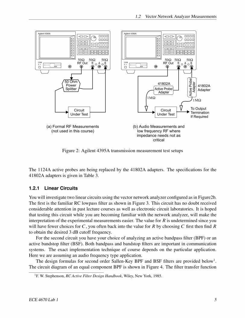
1.2 Vector Network Analyzer MeasurementsIn this portion of the experiment the 4395A will be used to characterize several linear systems. Inparticular linear two-port circuits will be analyzed in terms of the transmission parameters ampli-tude ratio (gain magnitude), phase, and group delay.
When making network analyzer measurements with this instrument the first step is to configurethe operating state to the proper measurement mode, activate appropriate source and receiver ports,select frequency sweep parameters, and display formats. See the quick start guide pp. 3-1 to 3-14.If you encounter difficulty or become frustrated trying to figure out the front panel controls, pleaseask the lab instructor for assistance.
The front panel signal ports of the 4395A are designed for 50 ohm impedance level measure-ments (source and load resistances). Typical radio-frequency (RF) transmission measurement testsetup are shown in Figure 2. For this course you will use the (b) configuration, since the circuityou test are below 100 MHz and the impedance levels are most often well above 50�.
Although not pafrt of this course, note that the 50 ohm power splitter of Figure 2a providesequal amplitude and phase output signals with a 50 ohm source resistance to each of the splitterports. This is not equivalent to a BNC tee! Receiver port R is used to measure the signal at the inputof the circuit under test while Receiver port B measures the circuit output. With the measurementformat set to Network: B/R (B the output and R the input) the complex ratio of these signalquantities as a function of sweep frequency is then formed by the analyzer. The analyzer screencan be configured to display two traces versus frequency, on a single plot or on a split plot (see the4395A operators manual p. 6-3). For transmission measurements the typical display format wouldbe the magnitude of the ratio in dB and the phase or group delay, which on the 4395A are displayformats LOG MAG, PHASE, DELAY and T/R(dB)-� ).
For audio frequency circuits, which is the subject of this portion of the lab, we need a higherimpedance level for making measurements. The setup shown in Figure 2.1b, which uses impedancetransforming adapters or active probes on the receiver inputs, is more appropriate for audio mea-surements. The Agilent 41802A input adapter allows an ordinary 1M� scope probe to be usedas an input device via an active network impedance transformation. The active probes HP 1124Atransform the 50 ohm input impedance level to 1 M� shunted by 10 picofarads. The analyzerusable measurement bandwidth is reduced to about 100 MHz with both the 41802A and 1124A.
ECE 4670 Lab 1 4
1.2 Vector Network Analyzer Measurements
Agilent 4395A
0 1 . . . .RF OutLine R BA
50 OhmPowerSplitter
CircuitUnder Test
Active Probe/Adapter
To OutputTerminationIf Required
(a) Formal RF Measurements (b) Audio Measurements and
Activ
e Pr
obe/
Adap
ter
Agilent 4395A
0 1 . . . .RF OutLine R BA
CircuitUnder Test
41802AAdapter
(not used in this course) low frequency RF whereimpedance needs not as
50Ω 50Ω 50Ω 50Ω
1MΩ 1MΩ
41802A
critical
50Ω 50Ω
Figure 2: Agilent 4395A transmission measurement test setups
The 1124A active probes are being replaced by the 41802A adapters. The specifications for the41802A adapters is given in Table 3.
1.2.1 Linear Circuits
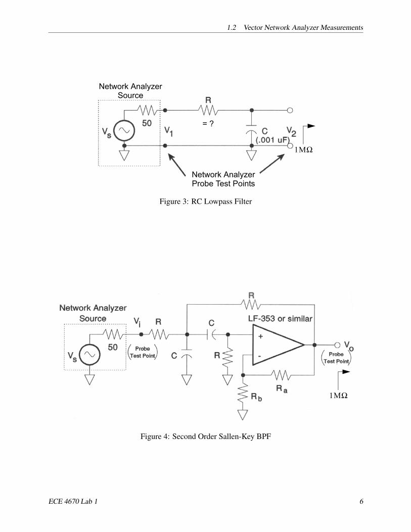
You will investigate two linear circuits using the vector network analyzer configured as in Figure2b.The first is the familiar RC lowpass filter as shown in Figure 3. This circuit has no doubt receivedconsiderable attention in past lecture courses as well as electronic circuit laboratories. It is hopedthat testing this circuit while you are becoming familiar with the network analyzer, will make theinterpretation of the experimental measurements easier. The value forR is undetermined since youwill have fewer choices for C , you often back into the value for R by choosing C first then find Rto obtain the desired 3 dB cutoff frequency.
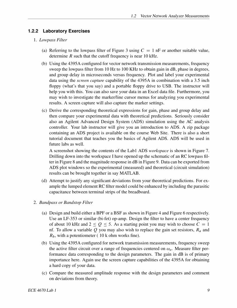
For the second circuit you have your choice of analyzing an active bandpass filter (BPF) or anactive bandstop filter (BSF). Both bandpass and bandstop filters are important in communicationsystems. The exact implementation technique of course depends on the particular application.Here we are assuming an audio frequency type application.
The design formulas for second order Sallen-Key BPF and BSF filters are provided below1.The circuit diagram of an equal component BPF is shown in Figure 4. The filter transfer function
1F. W. Stephenson, RC Active Filter Design Handbook, Wiley, New York, 1985.
where !o is the filter center frequency, Q, is the resonator quality factor related to the 3 dB band-width, and K is the amplifier voltage gain. In particular from (6) notice how Q and K are related.The design equations are
!o D
p2
RC(5)
Q D
p2
4 �KD
fo
BW(6)
K D 1CRa
Rb
(7)
Note that the filter gain at center frequency is given by
H.j!o/ DK
4 �K(8)
A general BPF frequency response showing the relation betweenQ and BW is shown in Figure 5a.The schematic of the Sallen-Key BSF is shown in Figure 6. The filter transfer function is given by
H.s/ DK.s2 C !2
o/
s2 C!o
Qs C !2
o
(9)
The parameters !o, Q, and K have the same meaning as in the BPF case except the design equa-tions forD !o and Q are now
!o D1
RC(10)
Q D1
4 � 2K(11)
The general BSF frequency response and bandwidth definitions are shown in Figure 5b.
ECE 4670 Lab 1 7
1.2 Vector Network Analyzer Measurements
f2f1 f0
H j
f2f1 f0
H jK
K2
-------
0 f
BWf0Q----=
f
K4 K–-------------
K 24 K–---------------
0
BWf0Q----=
Figure 5: BPF and BSF Frequency Response and Bandwidth Definitions
1MΩ
R/2
Figure 6: Second Order Sallen-Key BSF
ECE 4670 Lab 1 8
1.2 Vector Network Analyzer Measurements
1.2.2 Laboratory Exercises
1. Lowpass Filter
(a) Referring to the lowpass filter of Figure 3 using C D 1 nF or another suitable value,determine R such that the cutoff frequency is near 10 kHz.
(b) Using the 4395A configured for vector network transmission measurements, frequencysweep the lowpass filter from 10 Hz to 100 KHz to obtain gain in dB, phase in degrees,and group delay in microseconds versus frequency. Plot and label your experimentaldata using the screen capture capability of the 4395A in combination with a 3.5 inchfloppy (what’s that you say) and a portable floppy drive to USB. The instructor willhelp you with this. You can also save your data in an Excel data file. Furthermore, youmay wish to investigate the marker/line cursor menus for analyzing you experimentalresults. A screen capture will also capture the marker settings.
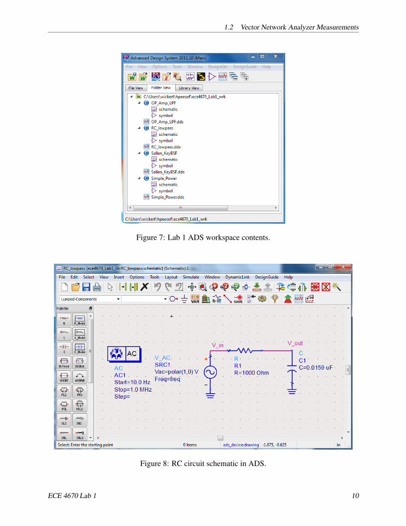
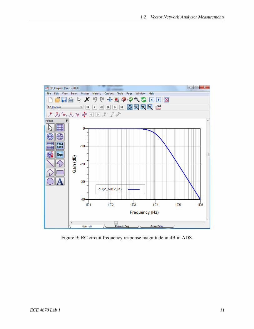
(c) Derive the corresponding theoretical expressions for gain, phase and group delay andthen compare your experimental data with theoretical predictions. Seriously consideralso an Agilent Advanced Design System (ADS) simulation using the AC analysiscontroller. Your lab instructor will give you an introduction to ADS. A zip packagecontaining an ADS project is available on the course Web Site. There is also a shorttutorial document that teaches you the basics of Agilent ADS. ADS will be used infuture labs as well.A screenshot showing the contents of the Lab1 ADS workspace is shown in Figure 7.Drilling down into the workspace I have opened up the schematic of an RC lowpass fil-ter in Figure 8 and the magnitude response in dB in Figure 9. Data can be exported fromADS plot windows so the experimental (measured) and theoretical (circuit simulation)results can be brought together in say MATLAB.
(d) Attempt to justify any significant deviations from your theoretical predictions. For ex-ample the lumped element RC filter model could be enhanced by including the parasiticcapacitance between terminal strips of the breadboard.
2. Bandpass or Bandstop Filter
(a) Design and build either a BPF or a BSF as shown in Figure 4 and Figure 6 respectively.Use an LF-353 or similar (bi-fet) op-amp. Design the filter to have a center frequencyof about 10 kHz and 2 � Q � 5. As a starting point you may wish to choose C D 1
nf. To allow a variable Q you may also wish to replace the gain set resistors, Ra andRb, with a potentiometer ( 10 k ohm works fine).
(b) Using the 4395A configured for network transmission measurements, frequency sweepthe active filter circuit over a range of frequencies centered on !o. Measure filter per-formance data corresponding to the design parameters. The gain in dB is of primaryimportance here. Again use the screen capture capabilities of the 4395A for obtaininga hard copy of your data.
(c) Compare the measured amplitude response with the design parameters and commenton deviations from theory.
ECE 4670 Lab 1 9
1.2 Vector Network Analyzer Measurements
Figure 7: Lab 1 ADS workspace contents.
Figure 8: RC circuit schematic in ADS.
ECE 4670 Lab 1 10
1.2 Vector Network Analyzer Measurements
Figure 9: RC circuit frequency response magnitude in dB in ADS.
ECE 4670 Lab 1 11
1.2 Vector Network Analyzer Measurements
(d) To obtain a better understanding of the theoretical circuit performance simulate thecircuit using ADS (see the Lab workspace for a prebuilt model you can play with). Thelab PC’s have ADS installed. Additional tutorial notes and screencasts on using ADScan be found on Dr. Wickert’s ECE 5250/4250 Web Site.
(e) Why is it impractical to obtain high Q’s from these circuits ?