ECE 4670 Spring 2014 Lab 4 Radio Receivers for Analog and Digital Modulation 1 Introduction This lab explores superheterodyne single and dual conversion receiver subsystems for analog and digital modulation. Two VHF (30–300 MHz) FM receivers are considered. The first receiver employes a wideband (about 200 kHz) IF subsystem centered at 10.7 MHz, while the second employes a narrowband (about 10 kHz) IF subsystem centered at 455 kHz. The narrowband FM receiver also utilizes dual conversion, with the first IF at 10.7 MHz and the second IF at 455 kHz. Both receivers have been constructed using readily available radio frequency integrated circuits (RFICs) from NXP semiconductor 1 . The receivers are presently in prototype form, constructed on an RF breadboard. In the future the receivers will be fabricated using a custom PCB. The high sensitivity of these receivers allows the wideband receiver to easily tune in FM broad- cast stations and the narrowband receiver to receive the Colorado Springs national weather service (NOAA) station, and lab broadcast frequency shift keyed (FSK) digital modulation. 1.1 Wideband FM Receiver The block diagram for the wideband receiver is given in Figure 1. The low-noise amplifier (LNA) is not implemented at this time, nor is the front-end bandpass filter (BPF). A short wire (clip lead) will serve as the antenna in the experiment. The receiver requires and external local oscillator !"# % &'( )*+,-*./01 " u (23453.67 850,-+0-32 9:;< 8=> =-?@ A/-. B( &'( C5DE7E,3F &'( &'( (8 G3F*H ! #$ ! %& ! '& " # $ %$ " ! #$ !-F-,32 Figure 1: Wideband FM receiver block diagram. (LO). In order to receive VHF signals, in particular FM broadcast which covers 87.5–108 MHz, the output of the Agilent 33250, which will serve as the LO, needs to be frequency doubled. The Agilent 33250 has a maximum frequency of 80 MHz, but with the doubler the effective maximum 1
Transcript
ECE 4670 Spring 2014 Lab 4Radio Receivers for Analog and Digital
Modulation
1 IntroductionThis lab explores superheterodyne single and dual conversion receiver subsystems for analog anddigital modulation. Two VHF (30–300 MHz) FM receivers are considered. The first receiveremployes a wideband (about 200 kHz) IF subsystem centered at 10.7 MHz, while the secondemployes a narrowband (about 10 kHz) IF subsystem centered at 455 kHz. The narrowband FMreceiver also utilizes dual conversion, with the first IF at 10.7 MHz and the second IF at 455 kHz.Both receivers have been constructed using readily available radio frequency integrated circuits(RFICs) from NXP semiconductor1. The receivers are presently in prototype form, constructed onan RF breadboard. In the future the receivers will be fabricated using a custom PCB.
The high sensitivity of these receivers allows the wideband receiver to easily tune in FM broad-cast stations and the narrowband receiver to receive the Colorado Springs national weather service(NOAA) station, and lab broadcast frequency shift keyed (FSK) digital modulation.
1.1 Wideband FM ReceiverThe block diagram for the wideband receiver is given in Figure 1. The low-noise amplifier (LNA)is not implemented at this time, nor is the front-end bandpass filter (BPF). A short wire (clip lead)will serve as the antenna in the experiment. The receiver requires and external local oscillator
!"#$%&'(
)*+,-*./01
! "(23453.67850,-+0-32
9:;<$8=>$=-?@$A/-.B($&'($C5DE7E,3F
&'(&'( (8G3F*H
!#$
!%&
!'& "# $% $
"!#$!-F-,32
Figure 1: Wideband FM receiver block diagram.
(LO). In order to receive VHF signals, in particular FM broadcast which covers 87.5–108 MHz,the output of the Agilent 33250, which will serve as the LO, needs to be frequency doubled. TheAgilent 33250 has a maximum frequency of 80 MHz, but with the doubler the effective maximum
1http://www.nxp.com/
1.1 Wideband FM Receiver
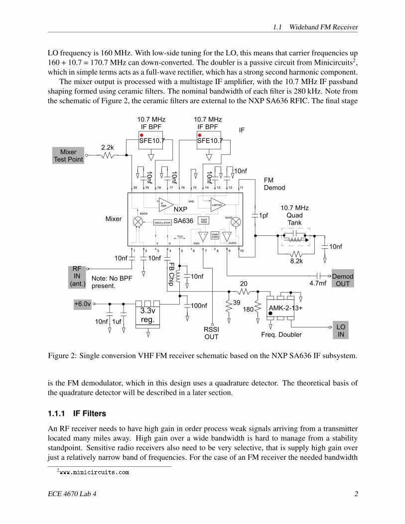
LO frequency is 160 MHz. With low-side tuning for the LO, this means that carrier frequencies up160 + 10.7 = 170.7 MHz can down-converted. The doubler is a passive circuit from Minicircuits2,which in simple terms acts as a full-wave rectifier, which has a strong second harmonic component.
The mixer output is processed with a multistage IF amplifier, with the 10.7 MHz IF passbandshaping formed using ceramic filters. The nominal bandwidth of each filter is 280 kHz. Note fromthe schematic of Figure 2, the ceramic filters are external to the NXP SA636 RFIC. The final stage
SFE10.7
AMK-2-13+
20 19 18 17 16 15 14 13 12 11
10987654321
FAST
IFAMP
E B
OSCILLATOR
LIMITER
MIXER
QUAD
+– +–
RSSI
GND
PWRDWN
RSSI AUDIO
VCC
SA636
NXP
SFE10.7
8.2k
4.7mfDemod
OUT10nf
1pf
LOIN
10.7 MHzQuadTank
20
39180
RFIN
(ant.)
10nf 10nf
100nf+6.0v
10nf
10nf
10nf
10nf
2.2kMixer
Test Point
10.7 MHzIF BPF
10.7 MHzIF BPF
10nf
Mixer
IF
FMDemod
Freq. DoublerRSSIOUT
FB ChipNote: No BPF
present.
3.3vreg.1uf10nf
Figure 2: Single conversion VHF FM receiver schematic based on the NXP SA636 IF subsystem.
is the FM demodulator, which in this design uses a quadrature detector. The theoretical basis ofthe quadrature detector will be described in a later section.
1.1.1 IF Filters
An RF receiver needs to have high gain in order process weak signals arriving from a transmitterlocated many miles away. High gain over a wide bandwidth is hard to manage from a stabilitystandpoint. Sensitive radio receivers also need to be very selective, that is supply high gain overjust a relatively narrow band of frequencies. For the case of an FM receiver the needed bandwidth
2www.minicircuits.com
ECE 4670 Lab 4 2
1.1 Wideband FM Receiver
is the bandwidth of the modulated message signal following a Carson’s rule analysis. In the FMbroadcast band stations are spaced every 200 kHz at odd 100 kHz spacings, e.g., 101.1 MHz, 99.3MHz, etc. From Wikipedia3 the one-sided baseband spectral occupancy is around 100 KHz beforebeing frequency modulated onto the carrier, as shown in Figure 3. The dominant baseband signalsare the L C R and L � R audio signals. The peak frequency deviation is 75 kHz. If we apply
Figure 3: One-sided FM broadcast spectrum including the various subcarrier services.
Carson’s rule to just the LC R signal, which has a nominal bandwidth of 15 Khz, we arrive at amodulated bandwidth of
BRF D 2.D C 1/W D 2
�75
15C 1
�15 D 180 kHz: (1)
When the L � R for FM stereo is included along with the other services, e.g. radio data service(RDS) at 57 kHz, the occupied spectrum must still be within a 200 kHz wide footprint.
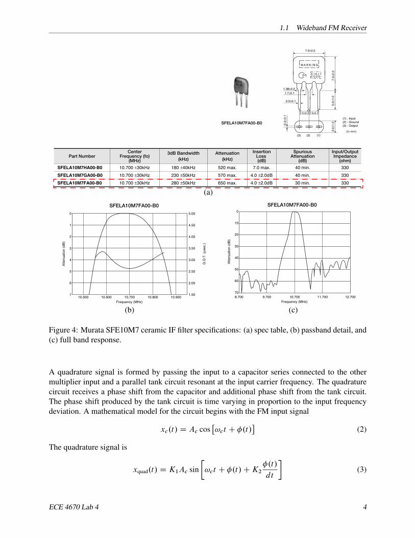
We desire an IF filter characteristic which passes only the signal/station of interest, rejectingall adjacent signals. A realizable IF filter will transition from passband to stopband over a finiteband of frequencies. The ceramic filters employed in the wideband receiver design are wider thanneeded, being that thy have a 3 dB bandwidth of 280 kHz. The filter specifications and plots of themagnitude and group delay response are shown in Figure 4.
1.1.2 Quadrature Demodulator
In analog integrated circuits used for FM radio receivers and the like, an FM demodulator known asa quadrature detector or quadrature discriminator, is quite popular. The schematic for the detectoris shown in Figure 5. The input FM signal connects to one port of a multiplier (product device).
Figure 4: Murata SFE10M7 ceramic IF filter specifications: (a) spec table, (b) passband detail, and(c) full band response.
A quadrature signal is formed by passing the input to a capacitor series connected to the othermultiplier input and a parallel tank circuit resonant at the input carrier frequency. The quadraturecircuit receives a phase shift from the capacitor and additional phase shift from the tank circuit.The phase shift produced by the tank circuit is time varying in proportion to the input frequencydeviation. A mathematical model for the circuit begins with the FM input signal
xc.t/ D Ac cos�!ct C �.t/
�(2)
The quadrature signal is
xquad.t/ D K1Ac sin�!ct C �.t/CK2
�.t/
dt
�(3)
ECE 4670 Lab 4 4
1.1 Wideband FM Receiver
CHAPTER 3. ANALOG MODULATION
FM Quadrature Detectors
C1
CpLp
xc(t)
xquad(t)
xout(t)
Tank circuit tuned to fc
Usually a lowpass filter is added here
Quadrature detector schematic
• In analog integrated circuits used for FM radio receivers andthe like, an FM demodulator known as a quadrature detectoror quadrature discriminator, is quite popular
• The input FM signal connects to one port of a multiplier (prod-uct device)
• A quadrature signal is formed by passing the input to a capaci-tor series connected to the other multiplier input and a paralleltank circuit resonant at the input carrier frequency
• The quadrature circuit receives a phase shift from the capacitorand additional phase shift from the tank circuit
• The phase shift produced by the tank circuit is time varying inproportion to the input frequency deviation
• A mathematical model for the circuit begins with the FM inputsignal
xc(t) = Ac[ωct + φ(t)]
3-72 ECE 5625 Communication Systems I
Figure 5: Quadrature detector schematic.
where the constants K1 and K2 are determined by circuit parameters. The multiplier output, as-suming a lowpass filter removes the sum terms, is
xout.t/1
2K1A
2c sin
�K2
d�.t/
dt
�(4)
By proper choice ofK2 the argument of the sin function is small, and a small angle approximationyields
xout.t/ '1
2K1K2A
2c
d�.t/
dtD1
2K1K2A
2cKDm.t/ (5)
1.1.3 Laboratory Exercises
1. The Colorado Springs market has a lot of FM broadcast stations. Several of them are likelyfamiliar to you. Set-up the Agilent 4395A spectrum analyzer with a VHF flex antenna con-nected to a 50 ohm input, as shown in Figure 6. Set the span to 87.5 to 108 MHz. This willallow you to see the entire FM broadcast spectrum. At this resolution each FM station willappear as a spectral line. Count the number of strong signals you see. For a few stations ver-ify using the marker that the center frequency of each station falls at an odd multiple of 100kHz and that the minimum spacing between stations is thus 200 kHz. Just from the spectrumanalyzer display, and your knowledge of FM stations in the Colorado Springs market, clearlyidentify one of your favorite stations by setting the marker at the station center frequency.
2. Spectrally zoom into one of the stronger stations and measure the approximate occupiedspectral bandwidth. Does it conform to needs of the 200 kHz spacing rule? The spectrumwill be changes as the applied modulation, e.g. music or talking changes over time.
3. In the next step you will power up the wideband receiver. You will need to know how to setthe LO frequency to receive FM broadcast stations. Develop two formulas for determiningthe required LO frequency to receive a station using either high-side or low-side LO tuning.Your functions should take as input the desired station frequency, e.g., 99.1 MHz and returnthe LO frequency. You need to take into account the fact that the LO frequency is doubled,as shown in Figure 1.
ECE 4670 Lab 4 5
1.1 Wideband FM Receiver
Agilent 4395A
0 1 . . . .RF OutLine R BA
Agilent 4395A
VHFFlexAntenna
Span 87.5 to 108 MHz to see availableFM broadcast stations in Colorado Springs
Figure 6: Agilent 4395A spectrum analyzer with VHF flex antenna mounted at an input port, toobserve the FM broadcast signals present on the 87.5 – 108 MHz band.
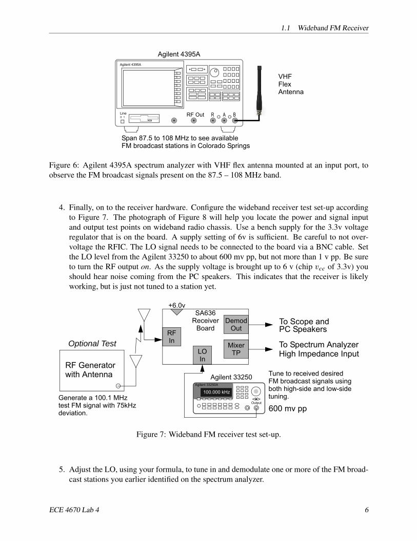
4. Finally, on to the receiver hardware. Configure the wideband receiver test set-up accordingto Figure 7. The photograph of Figure 8 will help you locate the power and signal inputand output test points on wideband radio chassis. Use a bench supply for the 3.3v voltageregulator that is on the board. A supply setting of 6v is sufficient. Be careful to not over-voltage the RFIC. The LO signal needs to be connected to the board via a BNC cable. Setthe LO level from the Agilent 33250 to about 600 mv pp, but not more than 1 v pp. Be sureto turn the RF output on. As the supply voltage is brought up to 6 v (chip vcc of 3.3v) youshould hear noise coming from the PC speakers. This indicates that the receiver is likelyworking, but is just not tuned to a station yet.
Agilent 33250A
Output
100.000 kHz
Agilent 33250
SA636Receiver
RFIn
LOIn
DemodOut
MixerTP
BoardTo Scope andPC Speakers
To Spectrum AnalyzerHigh Impedance Input
600 mv pp
RF Generatorwith Antenna
Generate a 100.1 MHztest FM signal with 75kHzdeviation.
Tune to received desiredFM broadcast signals usingboth high-side and low-sidetuning.
+6.0v
Optional Test
Figure 7: Wideband FM receiver test set-up.
5. Adjust the LO, using your formula, to tune in and demodulate one or more of the FM broad-cast stations you earlier identified on the spectrum analyzer.
ECE 4670 Lab 4 6
1.2 Narrowband Receiver
Mini CircuitsAMK-2-13+
LO Inputto Doubler
Freq. Doubler
ReceiverInput (Ant.)
Detector (audio)Output
SA636RadioChip
RSSIOutput
Mixertestpoint
10.7 MHzceramic BPFs
QuadratureDetector Tank
+6vJack
Figure 8: Single conversion wideband VHF FM receiver based on the NXP SA636 RFIC.
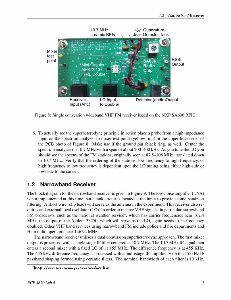
6. To actually see the superheterodyne principle in action place a probe from a high impedanceinput on the spectrum analyzer to mixer test point (yellow ring) in the upper left corner ofthe PCB photo of Figure 8. Make use if the ground pin (black ring) as well. Center thespectrum analyzer on 10.7 MHz with a span of about 200–400 kHz. As you tune the LO youshould see the spectra of the FM stations, originally seen at 87.5–108 MHz, translated downto 10.7 MHz. Verify that the ordering of the stations, low frequency to high frequency, orhigh frequency to low frequency is dependent upon the LO tuning being either high-side orlow-side to the carrier.
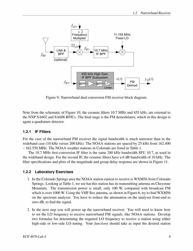
1.2 Narrowband ReceiverThe block diagram for the narrowband receiver is given in Figure 9. The low-noise amplifier (LNA)is not implemented at this time, but a tank circuit is located at the input to provide some bandpassfiltering. A short wire (clip lead) will serve as the antenna in the experiment. This receiver also re-quires and external local oscillator (LO). In order to receive VHF signals, in particular narrowbandFM broadcasts, such as the national weather service4, which has carrier frequencies near 162.4MHz, the output of the Agilent 33250, which will serve as the LO, again needs to be frequencydoubled. Other VHF band services using narrowband FM include police and fire departments andHam radio operators near 146.94 MHz.
The narrowband receiver utilizes a dual conversion superheterodyne approach. The first mixeroutput is processed with a single stage IF filter centered at 10.7 MHz. The 10.7 MHz IF signal thenenters a second mixer with a fixed LO of 11.155 MHz. The difference frequency is at 455 KHz.The 455 kHz difference frequency is processed with a multistage IF amplifier, with the 455kHz IFpassband shaping formed using ceramic filters. The nominal bandwidth of each filter is 10 kHz.
4http://www.nws.noaa.gov/nwr/nwrbro.htm
ECE 4670 Lab 4 7
1.2 Narrowband Receiver
!"#$%&'(
)*+,-*./01
! "(23453.67850,-+0-32
9::$;<=$<->?$@/-.A($&'($B5CD7D,3E
&'(&'( (8F3E*G
!#$
!%&
!'&(
"# $% $
"!#$HIJK$8<=A($&'(
HHJH::$8<=(-L3G$!M
!-E-,32
!'&"
Figure 9: Narrowband dual conversion FM receiver block diagram.
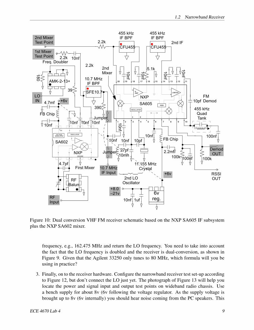
Note from the schematic of Figure 10, the ceramic filters 10.7 MHz and 455 kHz, are external tothe NXP SA602 and SA606 RFICs. The final stage is the FM demodulator, which in this design isagain a quadrature detector.
1.2.1 IF Filters
For the case of the narrowband FM receiver the signal bandwidth is much narrower than in thewideband case (10 kHz versus 200 kHz). The NOAA stations are spaced by 25 kHz from 162.400– 162.550 MHz. The NOAA weather stations in Colorado are listed in Table 1.
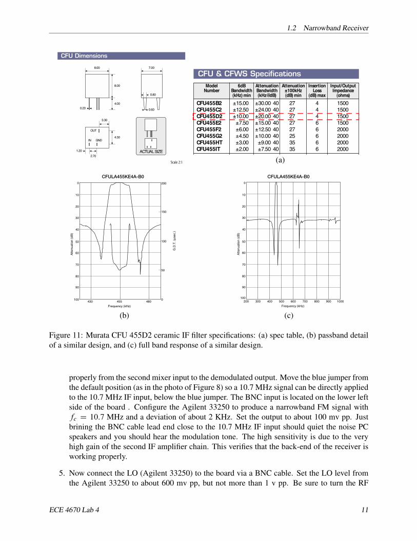
The 10.7 MHz first-conversion IF filter is the same 280 kHz bandwidth SFU 10.7, as used inthe wideband design. For the second IF, the ceramic filters have a 6 dB bandwidth of 10 kHz. Thefilter specifications and plots of the magnitude and group delay response are shown in Figure 11.
1.2.2 Laboratory Exercises
1. In the Colorado Springs area the NOAA station easiest to receive is WXM56 from ColoradoSprings. Looking at Table 1, we see hat this station has its transmitting antenna on CheyenneMountain. The transmission power is small, only 100 W, compared with broadcast FMwhich is over 1000 W. Using the VHF flex antenna, as shown in Figure 6, try to find WXM56on the spectrum analyzer. You have to reduce the attenuation on the analyzer front-end tozero dB, to find the signal.
2. In the next step you will power up the narrowband receiver. You will need to know howto set the LO frequency to receive narrowband FM signals, like NOAA stations. Developtwo formulas for determining the required LO frequency to receive a station using eitherhigh-side or low-side LO tuning. Your functions should take as input the desired station
ECE 4670 Lab 4 8
1.2 Narrowband Receiver
20 19 18 17 16 15 14 13 12 11
10987654321
RSSI
OSCILLATOR
IFAMP LIMITER
E B
SA605
8 7 6 5
4321
OSCILLATORVOLTAGEREGULATOR
GROUND
VCC
SA602
CFU455
SFE10.7
AMK-2-13+
CFU455
FB Chip
10nf 10nf 10nf 10nf
10.7 MHzIF BPF
10nf10nf
180
39
390
4.7pf
LOIN
455 kHzIF BPF
455 kHzIF BPF
5.1k
2nd MixerTest Point 2.2k
455 kHzQuadTank
FB Chip10nf
2.2mf
4.7mf +6v
+6v
10mh
10nf
27pf
10pf
11.155 MHzCrystal
100k100k 100nf
10nf
10nf
10nf
10nf
10pf
100nf
NXP
DemodOUT
RSSIOUT
Jumper
Freq. Doubler
2nd LOOscillator
First Mixer
2ndMixer
2nd IF
FMDemod
NXP
+8.06v
reg.1uf10nf –21v
RFBalun
RFInput
2.2k
10nf
10.7 MHzIF Input
Jumper
1st MixerTest Point 2.2k
Figure 10: Dual conversion VHF FM receiver schematic based on the NXP SA605 IF subsystemplus the NXP SA602 mixer.
frequency, e.g., 162.475 MHz and return the LO frequency. You need to take into accountthe fact that the LO frequency is doubled and the receiver is dual-conversion, as shown inFigure 9. Given that the Agilent 33250 only tunes to 80 MHz, which formula will you beusing in practice?
3. Finally, on to the receiver hardware. Configure the narrowband receiver test set-up accordingto Figure 12, but don’t connect the LO just yet. The photograph of Figure 13 will help youlocate the power and signal input and output test points on wideband radio chassis. Usea bench supply for about 8v (6v following the voltage regulator. As the supply voltage isbrought up to 8v (6v internally) you should hear noise coming from the PC speakers. This
ECE 4670 Lab 4 9
1.2 Narrowband Receiver
Table 1: NOAA stations throughout colorado.
indicates that the receiver is likely working, but is just not tuned to a station yet.
4. Before connecting the LO to the frequency doubler you will test that the receiver functions
ECE 4670 Lab 4 10
1.2 Narrowband Receiver
CFULA455KE4A-B0
100
40
30
20
10
0
Atte
nuat
ion (d
B)
0
50
100
150
200
G.D.
T. (µ
sec.)
430 455 480Frequency (kHz)
90
80
70
60
50
CFULA455KE4A-B0
100
40
30
20
10
0
Atte
nuat
ion (d
B)
200Frequency (kHz)
90
80
70
60
50
300 400 500 600 700 800 900 1000
Model 6dB Attenuation Attenuation Insertion Input/OutputNumber Bandwidth Bandwidth ±100kHz Loss Impedance
Figure 11: Murata CFU 455D2 ceramic IF filter specifications: (a) spec table, (b) passband detailof a similar design, and (c) full band response of a similar design.
properly from the second mixer input to the demodulated output. Move the blue jumper fromthe default position (as in the photo of Figure 8) so a 10.7 MHz signal can be directly appliedto the 10.7 MHz IF input, below the blue jumper. The BNC input is located on the lower leftside of the board . Configure the Agilent 33250 to produce a narrowband FM signal withfc D 10:7 MHz and a deviation of about 2 KHz. Set the output to about 100 mv pp. Justbrining the BNC cable lead end close to the 10.7 MHz IF input should quiet the noise PCspeakers and you should hear the modulation tone. The high sensitivity is due to the veryhigh gain of the second IF amplifier chain. This verifies that the back-end of the receiver isworking properly.
5. Now connect the LO (Agilent 33250) to the board via a BNC cable. Set the LO level fromthe Agilent 33250 to about 600 mv pp, but not more than 1 v pp. Be sure to turn the RF
ECE 4670 Lab 4 11
1.3 Appendix A: Data Sheet Highlights
Agilent 33250A
Output
100.000 kHz
Agilent 33250
SA602/SA605
RFIn
LOIn
DemodOut
Mixer 2TP
ReceiverTo Scope andPC Speakers
To Spectrum AnalyzerHigh Impedance Input
600 mv pp
RF Generatorwith Antenna
Generate a 163 MHz test FMsignal with 5kHz deviation.
Tune to received desiredFM broadcast signals usingboth high-side and low-sidetuning.
Generate a 163 MHz test FSK signal@ 5 kbps 1 – 4 kHz deviation
Board
+8–21v
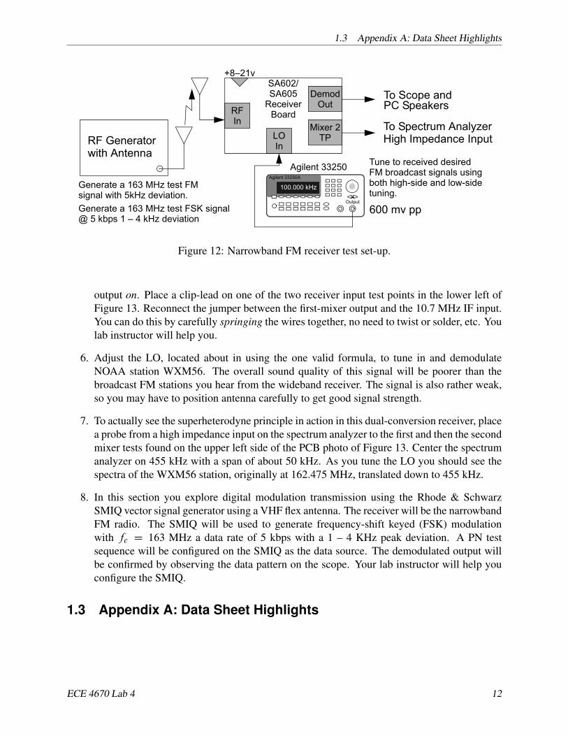
Figure 12: Narrowband FM receiver test set-up.
output on. Place a clip-lead on one of the two receiver input test points in the lower left ofFigure 13. Reconnect the jumper between the first-mixer output and the 10.7 MHz IF input.You can do this by carefully springing the wires together, no need to twist or solder, etc. Youlab instructor will help you.
6. Adjust the LO, located about in using the one valid formula, to tune in and demodulateNOAA station WXM56. The overall sound quality of this signal will be poorer than thebroadcast FM stations you hear from the wideband receiver. The signal is also rather weak,so you may have to position antenna carefully to get good signal strength.
7. To actually see the superheterodyne principle in action in this dual-conversion receiver, placea probe from a high impedance input on the spectrum analyzer to the first and then the secondmixer tests found on the upper left side of the PCB photo of Figure 13. Center the spectrumanalyzer on 455 kHz with a span of about 50 kHz. As you tune the LO you should see thespectra of the WXM56 station, originally at 162.475 MHz, translated down to 455 kHz.
8. In this section you explore digital modulation transmission using the Rhode & SchwarzSMIQ vector signal generator using a VHF flex antenna. The receiver will be the narrowbandFM radio. The SMIQ will be used to generate frequency-shift keyed (FSK) modulationwith fc D 163 MHz a data rate of 5 kbps with a 1 – 4 KHz peak deviation. A PN testsequence will be configured on the SMIQ as the data source. The demodulated output willbe confirmed by observing the data pattern on the scope. Your lab instructor will help youconfigure the SMIQ.
1.3 Appendix A: Data Sheet Highlights
ECE 4670 Lab 4 12
1.3 Appendix A: Data Sheet Highlights
11.155 MHzXTAL Osc.
LO Inputto doubler
RSSI
2nd Mixertest point
1st MixerOutput
Doubler
SA602MixerChip
ReceiverInput (Ant.)
Detector (audio) Output
SA605RadioChip
455 kHz 2nd IFceramic BPF
10.7 MHz 1st IFceramic BPF
QuadratureDetector Tank
output
FSKoutput
+6vJack
10.7 MHzIF InputJumper
External10.7 MHzIF Input
FSK/AudioJumper
Figure 13: Dual conversion VHF FM receiver based on the NXP SA602 and SA605.
ECE 4670 Lab 4 13
1.3 Appendix A: Data Sheet Highlights
Philips Semiconductors Product specification
SA636Low voltage high performance mixer FMIF system with high-speed RSSI
22003 Aug 01
DESCRIPTIONThe SA636 is a low-voltage high performance monolithic FM IFsystem with high-speed RSSI incorporating a mixer/oscillator, twolimiting intermediate frequency amplifiers, quadrature detector,logarithmic received signal strength indicator (RSSI), voltageregulator, wideband data output and fast RSSI op amps. The SA636is available in 20-lead SSOP (shrink small outline package).
The SA636 was designed for high bandwidth portablecommunication applications and will function down to 2.7 V. The RFsection is similar to the famous SA605. The data output has aminimum bandwidth of 600 kHz. This is designed to demodulatewideband data. The RSSI output is amplified. The RSSI output hasaccess to the feedback pin. This enables the designer to adjust thelevel of the outputs or add filtering.
SA636 incorporates a power-down mode which powers down thedevice when Pin 8 is LOW. Power down logic levels are CMOS andTTL compatible with high input impedance.
FEATURES• Wideband data output (600 kHz min.)
• Fast RSSI rise and fall times
• Low power consumption: 6.5 mA typ. at 3 V
• Mixer input to >500 MHz
• Mixer conversion power gain of 11 dB at 240 MHz
• Mixer noise figure of 12 dB at 240 MHz
• XTAL oscillator effective to 150 MHz (L.C. oscillator to 1 GHz localoscillator can be injected)
• 92 dB of IF Amp/Limiter gain
• 25 MHz limiter small signal bandwidth
• Temperature compensated logarithmic Received Signal StrengthIndicator (RSSI) with a dynamic range in excess of 90 dB
• RSSI output internal op amp
• Internal op amps with rail-to-rail outputs
• Low external component count; suitable for crystal/ceramic/LCfilters
• Excellent sensitivity: 0.54 µV into 50 ! matching network for12 dB SINAD (Signal to Noise and Distortion ratio) for 1 kHz tonewith RF at 240 MHz and IF at 10.7 MHz
• ESD hardened
• 10.7 MHz filter matching (330 !)
• Power-down mode (ICC = 200 µA)
PIN CONFIGURATION
RFIN
RF BYPASS
RSSIOUT
MIXER OUT
IF AMP IN
IF AMP OUT
GND
LIMITER IN
LIMITER OUT
DK Package
POWER DOWN CONTROL
DATA OUT
QUADRATURE IN
IF AMP DECOUPLING
IF AMP DECOUPLING
LIMITER DECOUPLING
LIMITER DECOUPLING
VCC
RSSI FEEDBACK
XTAL OSC (EMITTER)
XTAL OSC (BASE)
1
2
3
4
5
6
7
8
9
10
20
19
18
17
16
15
14
13
12
11
SR00491
Figure 1. Pin configuration
APPLICATIONS• DECT (Digital European Cordless Telephone)
• Digital cordless telephones
• Digital cellular telephones
• Portable high performance communications receivers
• Single conversion VHF/UHF receivers
• FSK and ASK data receivers
• Wireless LANs
ORDERING INFORMATIONDESCRIPTION TEMPERATURE RANGE ORDER CODE DWG #
20-Pin Plastic Shrink Small Outline Package (Surface-mount) –40 °C to +85 °C SA636DK SOT266–1
Figure 14: A portion (first page) of the NXP SA636 data sheet.
ECE 4670 Lab 4 14
1.3 Appendix A: Data Sheet Highlights
Figure 15: A portion (first page) of the NXP SA602 data sheet.
ECE 4670 Lab 4 15
1.3 Appendix A: Data Sheet Highlights
Philips Semiconductors Product specification
SA605High performance low power mixer FM IF system
21997 Nov 07 853-1401 18663
DESCRIPTIONThe SA605 is a high performance monolithic low-power FM IFsystem incorporating a mixer/oscillator, two limiting intermediatefrequency amplifiers, quadrature detector, muting, logarithmicreceived signal strength indicator (RSSI), and voltage regulator. TheSA605 combines the functions of Signetics’ SA602 and SA604A, butfeatures a higher mixer input intercept point, higher IF bandwidth(25MHz) and temperature compensated RSSI and limiterspermitting higher performance application. The SA605 is availablein 20-lead dual-in-line plastic, 20-lead SOL (surface-mountedminiature package) and 20-lead SSOP (shrink small outlinepackage).
The SA605 and SA615 are functionally the same device types. Thedifference between the two devices lies in the guaranteedspecifications. The SA615 has a higher ICC, lower input third orderintercept point, lower conversion mixer gain, lower limiter gain, lowerAM rejection, lower SINAD, higher THD, and higher RSSI error thanthe SA605. Both the SA605 and SA615 devices will meet the EIAspecifications for AMPS and TACS cellular radio applications.
For additional technical information please refer to application notesAN1994, 1995 and 1996, which include example applicationdiagrams, a complete overview of the product, and artwork forreference.
APPLICATIONS• Cellular radio FM IF
• High performance communications receivers
• Single conversion VHF/UHF receivers
• SCA receivers
• RF level meter
• Spectrum analyzer
• Instrumentation
• FSK and ASK data receivers
• Log amps
• Wideband low current amplification
PIN CONFIGURATION
RFIN 1RF BYPASS 2XTAL OSC 3XTAL OSC 4
MUTEIN 5
RSSIOUT 7
20 MIXER OUT
19
18 IF AMP IN
17
16 IF AMP OUT
15 GND
14 LIMITER IN
13
12
11 LIMITER OUT
VCC 6
MUTED AUDIO OUT 8
UNMUTED AUDIO OUT 9
QUADRATURE IN 10
IF AMP DECOUPLING
IF AMP DECOUPLING
LIMITER DECOUPLING
LIMITER DECOUPLING
N, D and DK Packages
SR00335
Figure 1. Pin Configuration
FEATURES• Low power consumption: 5.7mA typical at 6V
• Mixer input to >500MHz
• Mixer conversion power gain of 13dB at 45MHz
• Mixer noise figure of 4.6dB at 45MHz
• XTAL oscillator effective to 150MHz (L.C. oscillator to 1GHz localoscillator can be injected)
• 102dB of IF Amp/Limiter gain
• 25MHz limiter small signal bandwidth
• Temperature compensated logarithmic Received Signal StrengthIndicator (RSSI) with a dynamic range in excess of 90dB
• Two audio outputs - muted and unmuted
• Low external component count; suitable for crystal/ceramic/LCfilters
• Excellent sensitivity: 0.22µV into 50! matching network for 12dBSINAD (Signal to Noise and Distortion ratio) for 1kHz tone with RFat 45MHz and IF at 455kHz
• SA605 meets cellular radio specifications
• ESD hardened
ORDERING INFORMATIONDESCRIPTION TEMPERATURE RANGE ORDER CODE DWG #
20-Pin Plastic Dual In-Line Package (DIP) –40 to +85°C SA605N SOT146-120-Pin Plastic Small Outline Large (SOL) package –40 to +85°C SA605D SOT163-120-Pin Plastic Shrink Small Outline Package (SSOP) –40 to +85°C SA605DK SOT266-1
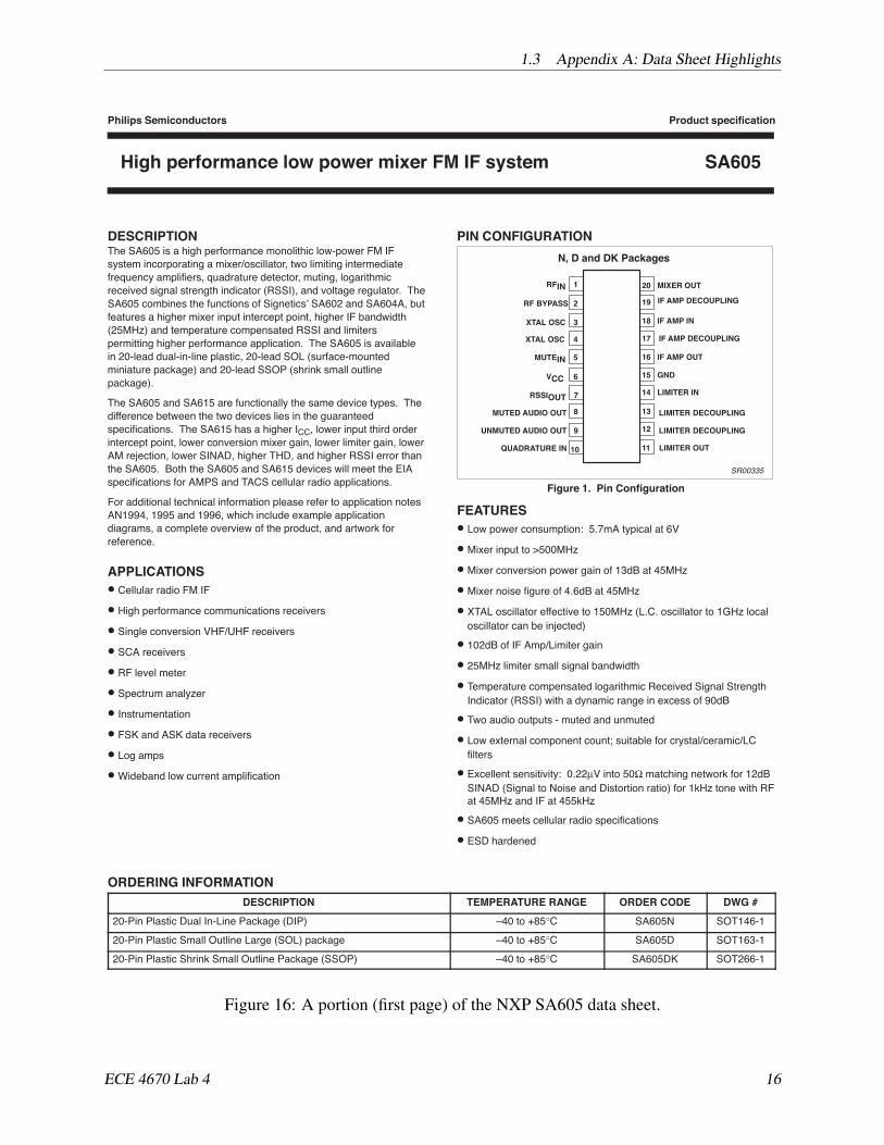
Figure 16: A portion (first page) of the NXP SA605 data sheet.


![Simulcast Radio Network Design - Home | College of ...mwickert/ece4890/lecture_notes/PericleTalk_fa2008.pdf[1]EIA TSB-88-B, “Wireless Communications Systems — Performance in Noise](https://static.documents.pub/doc/80x56/5e75bf257f40ac3ab32c6971/simulcast-radio-network-design-home-college-of-mwickertece4890lecturenotespericletalk.jpg)