ECS Interface Library User Guide 1MHz version Version: Release_v1.5 Created: 25/02/2006 Last modified: 19.06.2006 Prepared by: Hui Gong, Alex Gong, Hou Lei and Guido Haefeli Note that this document is strongly related to the TELL1 firmware version! 1
Transcript
ECS Interface Library User Guide
1MHz version
Version: Release_v1.5Created: 25/02/2006Last modified: 19.06.2006Prepared by: Hui Gong, Alex Gong, Hou Lei and Guido Haefeli
Note that this document is strongly related to the TELL1 firmware version!
1
Document status sheetRevision Date Reason for change
1.5 29.6.2006 Separate the ECS vhdl manual from the register and memory map,Update the ecs implementation to the current version! The ecs_reg register array is not available anymore in the components and registers.
1.4 7.4.2006 Change the position of the IP destination bits to be split over the last two bytes of the address (6 and 6)Remove MAC dest register in simu reg and add the two last bit of L0-EvCntAdd max cluster regAdd header correction register (en, strip0 and 1)Change that the destination MAC address does not changeUse one complete byte in the source MAC address to encode the port that is used to sent of the dataAdd interrupt bitAdd external trigger inputAdd max cluster cut register
1.3 6.4.2006 Add trigger fifo used word monitor regsAdd fem_dv_count monitor regAdd Reorder ram and reg for VeloAdd r,phi reorder bit for Velo in PP_CTRL_REG0
1.2 02/03/2006 Remove definition for L1T in GBE port selectAdded bank class register
1. Two Parts of Memories.............................................................................72. Significant Signal Description..................................................................73. ECS Memory Map....................................................................................7
3.1 Common ECS Memory Map....................................................................................73.1.1 GBE memory map.........................................................................................................................8
3.2 Internal Memory Map..............................................................................................93.3 External Memory Map (not used anymore for the TELL1 without L1Buffer as it is for LHCb in the 1MHz readout mode).....................................................................11
4. Detailed Description of Internal Memory Map....................................125. How to add an User Specific Register...................................................13
1) Define 5 constants in “user_tell1_lib. user_TELL1_type_map”......................................................132) Add the register component: ecs_register........................................................................................14
6. How to add an User Specific RAM, ROM and FIFO..........................166.1 How to add an User Specific RAM block...............................................................16
1) Define 4 constants in pp_fpga_user_memory_map.........................................................................162) Add the RAM component: xxx_ram................................................................................................173) Add the RAM multiplexer component: ecs_ram_mux.....................................................................174) Connect xxx_ram block with ecs_ram_mux component.................................................................19
6.2 How to add an User Specific ROM block..............................................................191) Define 4 constants in pp_fpga_user_memory_map.........................................................................192) Add the ROM component: xxx_rom................................................................................................19
6.3 How to add an User Specific FIFO block..............................................................201) Define 3 constants............................................................................................................................202) Add the FIFO component: xxx_fifo.................................................................................................203) Add the FIFO multiplexer component: ecs_fifo_mux.....................................................................214) Connect xxx_fifo block with ecs_fifo_mux component..................................................................23
3
7. Registers and RAM blocks Definition of PP-FPGA.............................247.1 Common Registers..................................................................................................24
7.2 User Specific Register.............................................................................................287.2.1 VELO specific registers (starts from 0x002000).......................................................................28VELO_ADCCLK_PHY_DLY_REGH ($0x002000)...........................................................................28VELO_ADCCLK_PHY_DLY_REGL ($0x002004)...........................................................................29VELO_ADCCLK_CYC_DLY_REG ($0x002008).............................................................................299 CLUS_PARA_REG ($0x00200C, $0x002010 …$0x00202C).........................................................29ADC_LINK_PROBE_REG ($0x002030)...........................................................................................30ADC_LINK_SYNC_REG ($0x002034).............................................................................................30VELO_PHI_REORDER_STRIP_CNT_REG ($0x002038)...............................................................31VELO_HEADER_CORRECTION_VALUE_STRIP_O_REG ($0x00203C)....................................31VELO_HEADER_CORRECTION_VALUE_STRIP_1_REG ($0x002040)......................................31VELO_CLUSTER_NUMBER_MAX_REG ($0x002044)..................................................................317.2.2 ST specific registers (starts from 0x003000).............................................................................31ORX_CTRL REG ($0x003000)...........................................................................................................3112 CLUS_PARA_REG ($0x003004, $0x003008 …$0x003030)........................................................32OPT_BEETLE_PROBE_REG ($0x003034)......................................................................................33OPT_BEETLE_SYNC_REG ($0x003038).........................................................................................33ST_HEADER_CORRECTION_VALUE_STRIP_O_REG ($0x00303C)..........................................34ST_HEADER_CORRECTION_VALUE_STRIP_1_REG ($0x003040)............................................34ST_CLUSTER_NUMBER_MAX_REG ($0x003044)........................................................................347.2.3 OT specific registers (starts from 0x000480)............................................................................347.2.4 CAL specific registers (starts from 0x0004C0).........................................................................347.2.5 MUON specific registers (starts from 0x000500)......................................................................34
7.4 User Specific RAM blocks......................................................................................367.2.3 VELO specific RAM (starts from 0x200000).............................................................................36
8. Registers and RAM blocks Definition of SyncLink-FPGA.................398.1 Common Registers..................................................................................................39
SEP_GEN_RAM (Address range: 0x200000 – 0x20FFFF)......................................578.4 User Specific RAM blocks......................................................................................57
9. I2C bus address definition......................................................................57I2C BUS 0 (mixed)..............................................................................................................................57I2C BUS 1 (FPGA bus)........................................................................................................................58I2C BUS 2 (A-Rx DAC bus)................................................................................................................58I2C BUS 3 (GBE Tx card bus).............................................................................................................59
Appendix: Example codes for C access........................................................59
6
1. Two Parts of Memories The memories employed by Tell1 DAQ are separated into two parts: Internal Memory and External Memory.
Internal memory includes Registers, FIFO, RAM and ROM on the FPGA chip.External memory includes L1 DDR SDRAM for PP-FPGA and QDR SRAM for
SyncLink-FPGA.
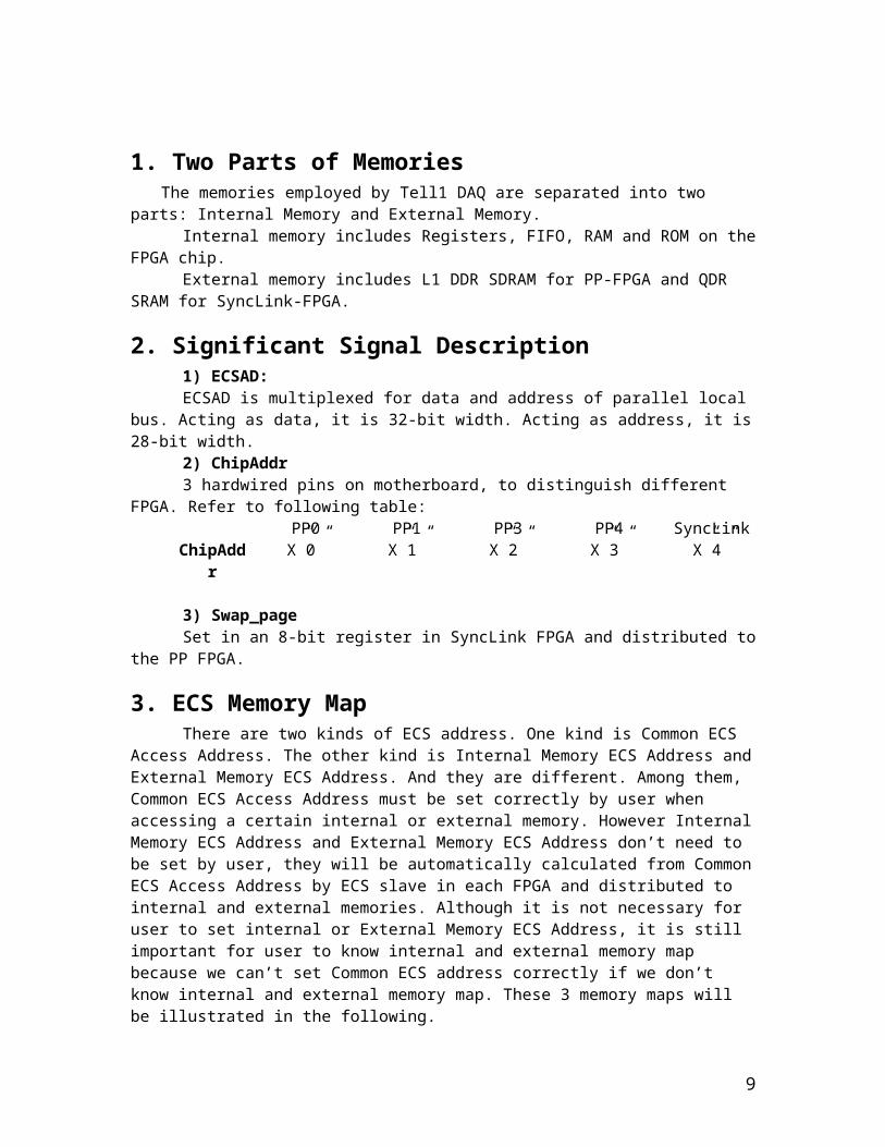
2. Significant Signal Description1) ECSAD: ECSAD is multiplexed for data and address of parallel local bus. Acting as data, it is 32-
bit width. Acting as address, it is 28-bit width.2) ChipAddr3 hardwired pins on motherboard, to distinguish different FPGA. Refer to following
table:PP0 PP1 PP3 PP4 SyncLink
ChipAddr X”0” X”1” X”2” X”3” X”4”
3) Swap_pageSet in an 8-bit register in SyncLink FPGA and distributed to the PP FPGA.
3. ECS Memory MapThere are two kinds of ECS address. One kind is Common ECS Access Address. The
other kind is Internal Memory ECS Address and External Memory ECS Address. And they are different. Among them, Common ECS Access Address must be set correctly by user when accessing a certain internal or external memory. However Internal Memory ECS Address and External Memory ECS Address don’t need to be set by user, they will be automatically calculated from Common ECS Access Address by ECS slave in each FPGA and distributed to internal and external memories. Although it is not necessary for user to set internal or External Memory ECS Address, it is still important for user to know internal and external memory map because we can’t set Common ECS address correctly if we don’t know internal and external memory map. These 3 memory maps will be illustrated in the following.
7
3.1 Common ECS Memory Map
Figure 3.1 Common ECS Memory Map Common ECS Memory Map is as Figure 3.1. In fact, Common ECS Access Address
composes of two parts: 28-bit ECSAD and 8-bit swap_page. The 28-bit ECSAD is generated by parallel local bus. And 8-bit swap page can be set in SyncLink FPGA and will be distributed to 4 PP FPGA. Swap_page is used to expand the memory space and merely used to access external memory because 28-bit ECSAD is adequate for accessing all the internal memory. The base address for GBE card is from 0x10000.
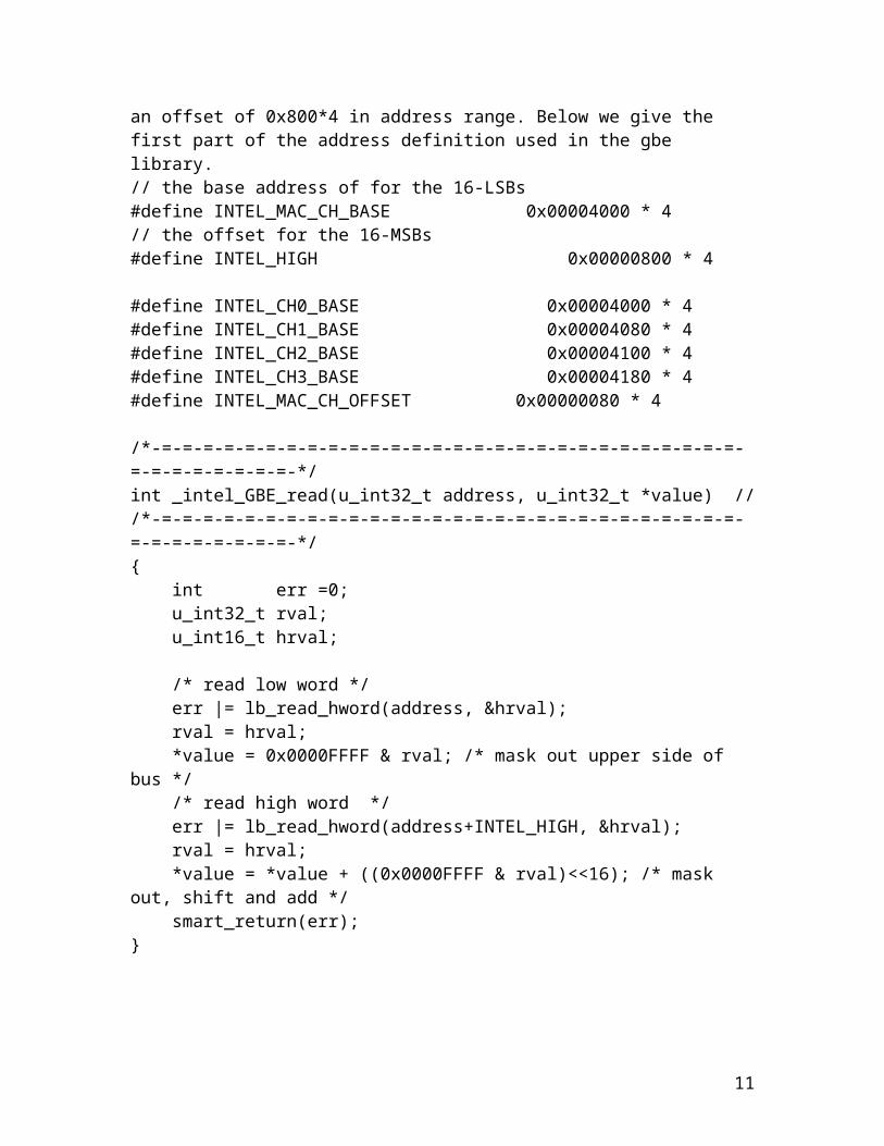
3.1.1 GBE memory mapTo clarify what the memory space for the GBE looks like we give the read function used to access the GBE MAC registers. Note that the data bus for the MAC is only 16-bit wide. The 16-LSBs of the registers are mapped at the memory space to one region and the 16-MSBs to an other. The two regions have an offset of 0x800*4 in address range. Below we give the first part of the address definition used in the gbe library.// the base address of for the 16-LSBs#define INTEL_MAC_CH_BASE 0x00004000 * 4// the offset for the 16-MSBs#define INTEL_HIGH 0x00000800 * 4
/* read low word */ err |= lb_read_hword(address, &hrval); rval = hrval; *value = 0x0000FFFF & rval; /* mask out upper side of bus */ /* read high word */ err |= lb_read_hword(address+INTEL_HIGH, &hrval); rval = hrval; *value = *value + ((0x0000FFFF & rval)<<16); /* mask out, shift and add */ smart_return(err);}
3.2 Internal Memory Map
9
Figure 3.2 Internal Memory Map for the PP_FPGA
At the moment, Internal Memory Map is like Figure 3.2 and the same for PP FPGA and SyncLink FPGA. From this figure, we know 24-bit Internal Memory ECS Address is used to access internal memory. As it was said, 24-bit Internal Memory ECS Address will be automatically calculated by ECS slave from Common ECS Access Address. The calculation algorithm is:
Internal_Memory_ECS_Address = ECSAD(23 .. 0) The condition that Internal Memory ECS Address is valid is:ChipAddr = "100" and ECSAD(27 downto 24) = "0001" --to access SyncLink FPGAECSAD(27) = 0 --to access internal memoryChipAddr = "000" and ECSAD(27 downto 24) = "0100" --to access PP0 FPGAChipAddr = "001" and ECSAD(27 downto 24) = "0101" --to access PP1 FPGAChipAddr = "010" and ECSAD(27 downto 24) = "0110" --to access PP2 FPGAChipAddr = "011" and ECSAD (27 downto 24) = "0111" --to access PP3 FPGA “ECSAD(27) = 0” indicates Common ECS Access Address is to access internal memory
of the FPGA whose ChipAddr is corresponding with current ECSAD(26..24). Swap_page is not used for accessing internal memory because ECSAD(27.. 0) is enough for accessing all the internal memories on the 5 FPGA.
According the algorithm above, ECS slave can calculate the Internal Memory ECS Address. On the contrary, user can set the Common ECS Access Address correctly according to the algorithm above when accessing a certain internal memory.
Internal memory map will be detailed illustrated in Chapter 4.
10
3.3 External Memory Map (not used anymore for the TELL1 without L1Buffer as it is for LHCb in the 1MHz readout mode)
Figure 3.3 External Memory Map
From Figure 3.3, we know that 32-bit External Memory ECS Address is used to access External Memory, so the total memory space is 4 GB for each FPGA.
However, only the lowest 27 bits are used by PP FPGA to access its external memory: L1 DDR SDRAM. So the actual external memory space of PP FPGA is 128M bytes (no more than 1 swap page). For SyncLink FPGA, only the lowest 20 bits are used to access its external memory: QDR SRAM. The actual external memory space used by SyncLink FPGA is 1M bytes (less than 1 swap page).
Although the memory space used by PP FPGA is different from SyncLink FPGA, the algorithm that ECS slave calculates 32-bit External Memory ECS Address from Common ECS Access Address obviously is identical:
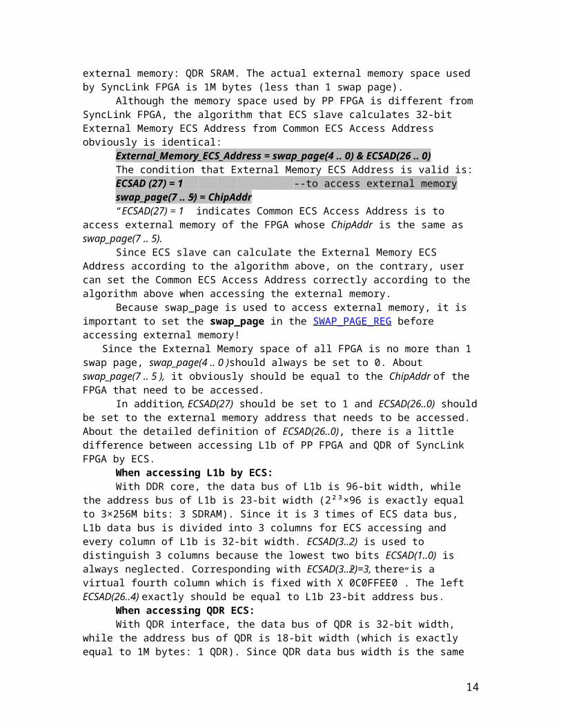
External_Memory_ECS_Address = swap_page(4 .. 0) & ECSAD(26 .. 0)The condition that External Memory ECS Address is valid is:ECSAD (27) = 1 --to access external memoryswap_page(7 .. 5) = ChipAddr“ECSAD(27) = 1” indicates Common ECS Access Address is to access external memory
of the FPGA whose ChipAddr is the same as swap_page(7 .. 5). Since ECS slave can calculate the External Memory ECS Address according to the
algorithm above, on the contrary, user can set the Common ECS Access Address correctly according to the algorithm above when accessing the external memory.
Because swap_page is used to access external memory, it is important to set the swap_page in the SWAP_PAGE_REG before accessing external memory!
11
Since the External Memory space of all FPGA is no more than 1 swap page, swap_page(4 .. 0 )should always be set to 0. About swap_page(7 .. 5 ), it obviously should be equal to the ChipAddr of the FPGA that need to be accessed.
In addition, ECSAD(27) should be set to 1 and ECSAD(26..0) should be set to the external memory address that needs to be accessed. About the detailed definition of ECSAD(26..0), there is a little difference between accessing L1b of PP FPGA and QDR of SyncLink FPGA by ECS.
When accessing L1b by ECS:With DDR core, the data bus of L1b is 96-bit width, while the address bus of L1b is 23-
bit width (2²³×96 is exactly equal to 3×256M bits: 3 SDRAM). Since it is 3 times of ECS data bus, L1b data bus is divided into 3 columns for ECS accessing and every column of L1b is 32-bit width. ECSAD(3..2) is used to distinguish 3 columns because the lowest two bits ECSAD(1..0) is always neglected. Corresponding with ECSAD(3..2)=3, there is a virtual fourth column which is fixed with X”0C0FFEE0”. The left ECSAD(26..4) exactly should be equal to L1b 23-bit address bus.
When accessing QDR ECS:With QDR interface, the data bus of QDR is 32-bit width, while the address bus of QDR
is 18-bit width (which is exactly equal to 1M bytes: 1 QDR). Since QDR data bus width is the same as ECS data bus, ECSAD(19..2) should be equal to QDR 18-bit address bus while both ECSAD(26..20) and ECSAD(1..0) should be fixed with 0.
4. Detailed Description of Internal Memory MapThe internal memories are separated into four parts: Common Registers, User Specific
Registers, Common RAM blocks and User Specific RAM blocks as Figure 3.2 Internal Memory Map. For illustrating easily, the RAM, ROM and FIFO are all called as RAM blocks in this chapter.
The number of Common Registers, User Specific Registers, Common RAM blocks and User Specific RAM blocks is defined by four constants respectively: N_REG_COMMON, N_REG_USER, N_RAM_COMMON and N_RAM_USER.
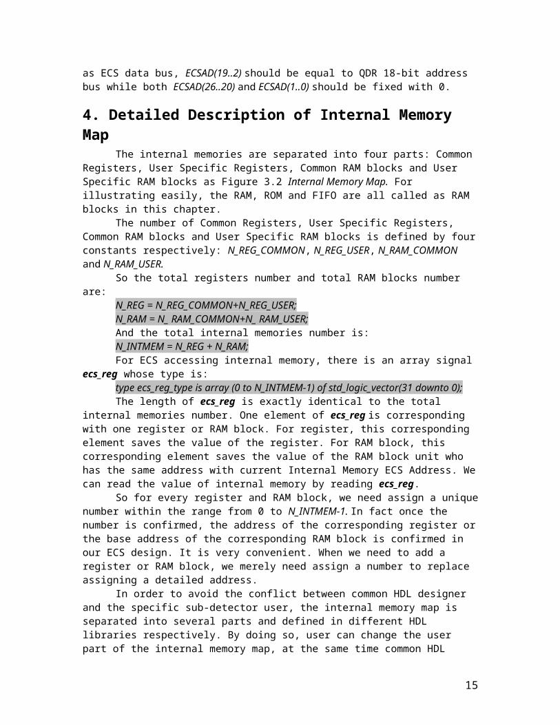
So the total registers number and total RAM blocks number are:N_REG = N_REG_COMMON+N_REG_USER;N_RAM = N_ RAM_COMMON+N_ RAM_USER;And the total internal memories number is:N_INTMEM = N_REG + N_RAM;For ECS accessing internal memory, there is an array signal ecs_reg whose type is:type ecs_reg_type is array (0 to N_INTMEM-1) of std_logic_vector(31 downto 0);The length of ecs_reg is exactly identical to the total internal memories number. One
element of ecs_reg is corresponding with one register or RAM block. For register, this corresponding element saves the value of the register. For RAM block, this corresponding element saves the value of the RAM block unit who has the same address with current Internal Memory ECS Address. We can read the value of internal memory by reading ecs_reg.
So for every register and RAM block, we need assign a unique number within the range from 0 to N_INTMEM-1. In fact once the number is confirmed, the address of the corresponding register or the base address of the corresponding RAM block is confirmed in our ECS design. It is very convenient. When we need to add a register or RAM block, we merely need assign a number to replace assigning a detailed address.
In order to avoid the conflict between common HDL designer and the specific sub-detector user, the internal memory map is separated into several parts and defined in different HDL libraries respectively. By doing so, user can change the user part of the internal memory
12
map, at the same time common HDL designer can change the common part of internal memory map without conflict.
Generally there are two packages to define the whole memory map of TELL1: common_tell1_lib. common_TELL1_type_map user_tell1_lib. user_TELL1_type_map.
It is clear that the detector specific ECS items should be defined in the user_tell1_lib package.
For each FPGA, there are 4 ECS regions: Common register region. User register region Common RAM/ROM region User RAM/ROM region.
For register region, each item occupies 4 bytes. For RAM/ROM region, each item occupies 8192 bytes.The number of existing registers are defined in the vhdl package called common_TELL1_type_map and is found in common_tell1_lib
5. How to add an User Specific RegisterThis chapter is specially written for user and illustrates how to add a user specific
register. Certainly the common HDL designer can refer to this chapter to add a common register because it is very similar as adding a user specific register.
For example, if user needs to add a user specific register for PP-FPGA, we can do as following:
1) Define 5 constants in “user_tell1_lib. user_TELL1_type_map”Following is an example about the constant definition:
First give a proper name for the register as “XXX”, it is strongly recommended to add the detector name as the prefix to avoid any possible naming-confliction (the “detector” name can be as VELO, ST, OT, Cal, Muon). Then assign 5 constants for this register.
detector_XXX_REG_N : decided by the parameter num detector_XXX_REG_ADDR: decided by the parameter num
The “num” is the unique index of the register, starts from 0 for each detector. The detector_REG_START and detector_REG_BADDR are pre-defined in the common_tell1_lib package.
detector_XXX_REG_NDATA : the width of the register. detector_XXX_REG_DEFAULT: the default value of the register. detector_If XXX_REG_AUTO_RESET: when set true, the register will be
automatically return to default values one cycles after written. In principle, we can define it as false.
Here is an example from ST:--[ST Specific registers]--
2) Add the register component: ecs_register Add ecs_register component from ecs_interface_lib.
Figure 5.1 ecs_register componentAfter adding ecs_register component into the HDL design, firstly we can assign the Generic
with the constant we have defined in pp_fpga_user_memory_map. Then we can add interface ports automatically by select Add Signal Stubs from clicking right mouse button on the component. Now it will be similar as Figure 5.2.
Figure 5.2 ecs_register component after first modificationSecondly, we should modify the clk port according to the clock domain where the
ecs_register component is used. If the current domain general clock is 40 MHz, we need to change clk and ecs_wrreq into clk_40 and ecs_wrreq_40 respectively. Then we change the reg port into xxx_reg, and replace REG_N_DATA with XXX_REG_N_DATA. Now the component will be like Figure 5.3, and we have finished adding ecs_register component.
14
Figure 5.3 finished ecs register componentAt last, we can use xxx_reg signal to control some other signals in the HDL design.
If the RAM block is defined inside a certain component, make sure the ECS signals are connected with ECS slave on the top layer. In principle we need to convert the ECS signals to IO ports in this case. It is similar to add other ECS accessible internal memory.
6. How to add an User Specific RAM, ROM and FIFOThis chapter is specially written for user too.Comparing with adding a register, it is a little more complicated for user to add an ECS
accessible user specific RAM, ROM or FIFO block, but it is not difficult. Following, they will be illustrated respectively.
6.1 How to add an User Specific RAM block For example, if we need to add an ECS accessible user specific RAM block for PP-
FPGA, we can do as following:
1) Define 4 constants in pp_fpga_user_memory_mapFollowing is an example about the constant definition:
First give a proper name for the RAM as “XXX”, it is strongly recommended to add the detector name as the prefix to avoid any possible naming-confliction (the “detector” name can be as VELO, ST, OT, Cal, Muon). Then assign 4 constants for this RAM.
detector_XXX_RAM_N : decided by the parameter num detector_XXX_RAM_ADDR : decided by the parameter num
The “num” is the unique index of the RAM, starts from 0 for each detector. The detector_RAM_START and detector_RAMBADDR are pre-defined in the common_tell1_lib package.
detector_XXX_RAM_N_ADDR: the width of RAM address. Note that the CCPC is default addressing in bytes while all addressing in TELL1 is in words thus the ECS address bus width has 2 bits more.
15
detector_XXX_RAM_N_DATA: the width of RAM data.
2) Add the RAM component: xxx_ramFollowing is an example of RAM block:
Figure 6.1 xxx_ram block
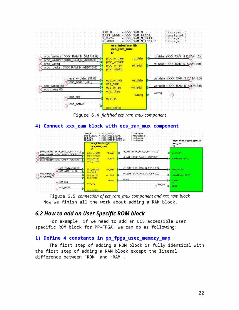
3) Add the RAM multiplexer component: ecs_ram_muxAdd ecs_ram_mux component from ecs_interface_lib.
Figure 6.2 ecs_ram_mux componentAfter adding ecs_ram_mux component into the HDL design, firstly we can assign the
Generic with the constant we have defined in pp_fpga_user_memory_map. When assigning the generic: N_ADDR, make sure to subtract 2 from XXX_RAM_N_ADDR. Then we can add interface ports automatically by select Add Signal Stubs from clicking right mouse button on the component. Now it will be similar as Figure 6.3.
16
Figure 6.3 ecs_ram_mux component after first modification Secondly, we should modify the ecs_wrreq and ecs_rdreq signal according to the clock
used by the xxx_ram block. If the xxx_ram block’s clock is 80 MHz, we need to change ecs_wrreq and ecs_rdreq into ecs_wrreq_80 and ecs_rdreq_80 respectively. Then we replace N_DATA and N_ADDR with XXX_RAM_N_DATA and XXX_RAM_N_ADDR–2 respectively. Now the component will be like Figure 6.4.
Those signals at the right of component can be modified according to the design requirement, which will be used to connect with xxx_ram block
Those signals whose name contains the word “proc” are another way for data flow processor to access the RAM block. If a certain processor need to access the RAM block, we need to appropriately connect those signals with the corresponding signals of the processor. If some proc-signals aren’t used, remove them and leave them unconnected which will be fed with defaulted value.
Figure 6.4 finished ecs_ram_mux component
17
4) Connect xxx_ram block with ecs_ram_mux component
Figure 6.5 connection of ecs_ram_mux component and xxx_ram block Now we finish all the work about adding a RAM block.
6.2 How to add an User Specific ROM block For example, if we need to add an ECS accessible user specific ROM block for PP-
FPGA, we can do as following:
1) Define 4 constants in pp_fpga_user_memory_mapThe first step of adding a ROM block is fully identical with the first step of adding a
RAM block except the literal difference between “ROM” and “RAM”.
2) Add the ROM component: xxx_rom
Figure 6.6 xxx_rom blockAfter adding xxx_rom block into the HDL design, we can add interface ports
automatically by select Add Signal Stubs from clicking right mouse button on the component. Now it will be similar as Figure 6.6.
Then modify xxx_rom block referring to Figure 6.7. The purpose of employing a yellow block is to pass the read data from the ROM block to the corresponding element of the signal array: ecs_reg, which is defined in the tell1_common_lib.
18
Figure 6.6 finished xxx_rom block
Now we can read the ROM block by ECS.
6.3 How to add an User Specific FIFO block For example, if we need to add an ECS accessible user specific FIFO block for PP-
FPGA, we can do as following:
1) Define 3 constants The FIFO can be treated as registers, but without the default value and auto reset feathers.
2) Add the FIFO component: xxx_fifoObviously, this component is generated and added according to the user’s requirement.
Following is an example of FIFO block:
19
Figure 6.7 xxx_fifo block
3) Add the FIFO multiplexer component: ecs_fifo_muxAdd ecs_fifo_mux component from ecs_interface_lib.
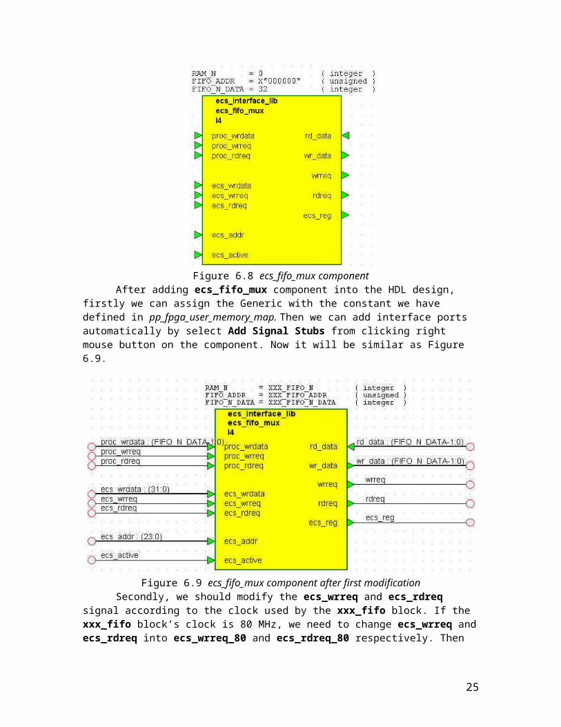
Figure 6.8 ecs_fifo_mux componentAfter adding ecs_fifo_mux component into the HDL design, firstly we can assign the
Generic with the constant we have defined in pp_fpga_user_memory_map. Then we can add interface ports automatically by select Add Signal Stubs from clicking right mouse button on the component. Now it will be similar as Figure 6.9.
Figure 6.9 ecs_fifo_mux component after first modification Secondly, we should modify the ecs_wrreq and ecs_rdreq signal according to the clock
used by the xxx_fifo block. If the xxx_fifo block’s clock is 80 MHz, we need to change ecs_wrreq and ecs_rdreq into ecs_wrreq_80 and ecs_rdreq_80 respectively. Then we replace FIFO_N_DATA with XXX_FIFO_N_DATA. Now the component will be like Figure 6.10.
20
Those signals at the right of component can be modified according to the design requirement, which will be used to connect with xxx_fifo block
Those signals whose name contains the word “proc” are another way for data flow processor to access the FIFO. If a certain processor needs to access the FIFO, we need to appropriately connect those signals with the corresponding signals of the processor. If some proc-signals aren’t used, remove them and leave them unconnected which will be fed with defaulted value.
Figure 6.10 finished ecs_fifo_mux component
4) Connect xxx_fifo block with ecs_fifo_mux component
Figure 6.11 connection of ecs_fifo_mux component and xxx_fifo block Now we finish all the work about adding a FIFO block.
21
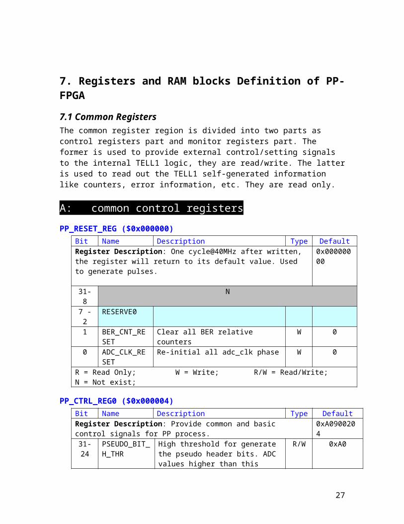
7. Registers and RAM blocks Definition of PP-FPGA
7.1 Common RegistersThe common register region is divided into two parts as control registers part and monitor registers part. The former is used to provide external control/setting signals to the internal TELL1 logic, they are read/write. The latter is used to read out the TELL1 self-generated information like counters, error information, etc. They are read only.
A: common control registers
PP_RESET_REG ($0x000000)Bit Name Description Type DefaultRegister Description: One cycle@40MHz after written, the register will return to its default value. Used to generate pulses.
0x00000000
31- 8 N7 - 2 RESERVE0
1 BER_CNT_RESET
Clear all BER relative counters W 0
0 ADC_CLK_RESET
Re-initial all adc_clk phase W 0
R = Read Only; W = Write; R/W = Read/Write; N = Not exist;
PP_CTRL_REG0 ($0x000004)Bit Name Description Type DefaultRegister Description: Provide common and basic control signals for PP process.
0xA0900204
31-24 PSEUDO_BIT_H_THR
High threshold for generate the pseudo header bits. ADC values higher than this value is treated as logic ‘1’.
R/W 0xA0
23-16 PSEUDO_BIT_L_THR
Low threshold for generate the pseudo header bits. ADC values lower than this value is treated as logic ‘0’.
R/W 0x90
15-12 READ_LINK_SEL
The monitor registers for each link share the same ECS address, this field is used to select a certain link’s register to read out.( 0-15 for ARX, 0-5 for ORX)
R/W 0
11 R_reorder Choose the R-sensor reordering for VELO 010 PHI_reorder Choose the Phi-sensor reordering for
VELO0
9 ZS_EN Enable/disable the zerosuppression suppression
1
8 CM_EN Enable/disable the common mode suppression
0
7 BER_EN Enable/Disable the Bit Error Rate test R/W 0
22
function ( For ORX only)6 DATA_GEN_E
NEnable/Disable the internal data generator to replace the actually detector data
R/W 0
5 FIR_EN Enable/disable the FIR ( ARX only) R/W 04 REORDER_EN (VELO only) R/W 03 PEDESTAL_U
PDATE_ENEnable/Disable the pedestal auto update feather, with which the pedestal can follow up the base line shift.
R/W 0
2 PEDESTAL_EN
Enable/Disable the pedestal subtraction R/W 1
1-0 DATA_SCALE_MODE
After pedestal subtraction, determines how to scale the 11bit down to 8bit0: saturate to -128 to 127 (VELO only)1: bit(8..1) (LSB remove)2: bit(9..2) (2LSB remove)3: bit(10..3) (3LSB remove)
R/W 00
R = Read Only; W = Write; R/W = Read/Write; N = Not exist;
PP_CTRL_REG1 ($0x000008)Bit Name Description Type DefaultRegister Description: Provide common and basic control signals for PP process.
0x00000020
31-8 RESERVE0 /7 header_correction_enable Enables the header correction
for the CMS algorithm for Velo and ST
R/W 0
6-0 CLUS_DERAN_USE_THR Threshold for cluster derandomizer(in events. VELO has max 256, OPT max 128)
R/W 0x20
R = Read Only; W = Write; R/W = Read/Write; N = Not exist;
ORX_CTRL REG ($0x00000C) Bit Name Description Type DefaultRegister Description: O-Rx control bits, bit error rate test mode 0x3F00000931- 30 RESERVED2 0029- 24 ORX_LCK_RE
FLock to reference output to TLK set 1 for normal operation
R/W 0x3F
23- 14 RESERVED1 000000000013- 8 ORX_LINK_DI
SABLEOne hot encoded disable signal for each optical link 1 = disable, 0 = enableSet 0 for normal operation
R/W 000000
7-6 RESERVE0 005 ORX_PRBS_E
N345Pseudo Random Bit Test Enable signal for Optical card channels: 3, 4, 5.0 = no pseudo random test1 = enable pseudo random test
R/W 0
23
4 ORX_LOOP_EN345
Internal loop-back enable signal for Optical card channels: 3, 4, 5.0 = disable loop-back, means standard operation.1 = enable Optical card internal loop-back
R/W 0
3 ORX_EN345 Device Enable signal for Optical card channels: 3, 4, 5.1 = Enable these 3 optical channels0 = Puts relative circuit of Optical card in power down mode.
R/W 1
2 ORX_PRBS_EN012
Pseudo Random Bit Test Enable signal for Optical card channels: 0, 1, 2.0 = no pseudo random test1 = enable pseudo random test
R/W 0
1 ORX_LOOP_EN012
Internal loop-back enable signal for Optical card channels: 0, 1, 2.0 = disable loop-back, means standard operation.1 = enable Optical card internal loop-back
R/W 0
0 ORX_EN012 Device Enable signal for Optical card channels: 0, 1, 2.1 = Enable these 3 optical channels0 = Puts relative circuit of Optical card in power down mode.
R/W 1
R = Read Only; W = Write; R/W = Read/Write; N = Not exist;
B: Common Monitor registers
CONSTANT_REG ($0x001000)Bit Name Description Type DefaultRegister Description: Constant informations Note31-24 Reserved R \7-4 DETECTOR_I
Dused to distinguish different synchronizer designs. Use 0x1 for Velo, 0x2 for ST, 0x3 for OT, 0x4 for Cal, 0x5 for
Muon, 0x6 L0MUON, 0x7 for L0DU, 0x8 L0PUS, 0x9 RICH
R \
3 RESERVE0 \2-0 CHIPADDR Hard-wired chip address. R \
R = Read Only; W = Write; R/W = Read/Write; N = Not exist;Note: depends on the version settings in common_TELL1_library and user_TELL1_library
EVT_ASSEM_CNT_REG ($0x001004)Bit Name Description Type DefaultRegister Description: 0x0000000031- 16 VARI_CNT OPX: event async count When start to
assemble event, all the enabled opt links should have an event data ready. If not, an
R \
24
event_async error occurs.ARX: event in count The number of actual events sent from detector. ( the number of FEM_dv )
15-0 EVT_OUT_CNT
The number of events assembled in the Rx part. R \
R = Read Only; W = Write; R/W = Read/Write; N = Not exist;
PP_TRIGGER_CNT_REG ($0x001008)Bit Name Description Type DefaultRegister Description: the number of trigger request and trigger get 0x00000000
31- 16 TRIGGER_REQ_CNT
The number of trigger request sent from this PP-FPGA to SL-FPGA R \
15-0 TRIGGER_IN_CNT
The number of trigger information sent from SL-FPGA to this PP-FPGA R \
R = Read Only; W = Write; R/W = Read/Write; N = Not exist;
PP_BANK_CNT_REG0 ($0x00100C)Bit Name Description Type DefaultRegister Description: the number of each bank assembled in this PP-FPGA 0x00000000
31- 16 INFO_BANK_CNT The number of information bank R \
15-0 CLUS_BANK_CNT The number of cluster bank R \
R = Read Only; W = Write; R/W = Read/Write; N = Not exist;
PP_BANK_CNT_REG1 ($0x001010)Bit Name Description Type DefaultRegister Description: the number of each bank assembled in this PP-FPGA 0x00000000
31- 16 ADC_BANK_CNT The number of adc value bank R \
15-8 PEDE_BANK_CNT The number of pedestal bank R \
7-0 RAW_BANK_CNT The number of raw bank R \
R = Read Only; W = Write; R/W = Read/Write; N = Not exist;
PP_EVENT_CNT_REG ($0x001014)Bit Name Description Type DefaultRegister Description: the number of events assembled in this PP-FPGA 0x00000000
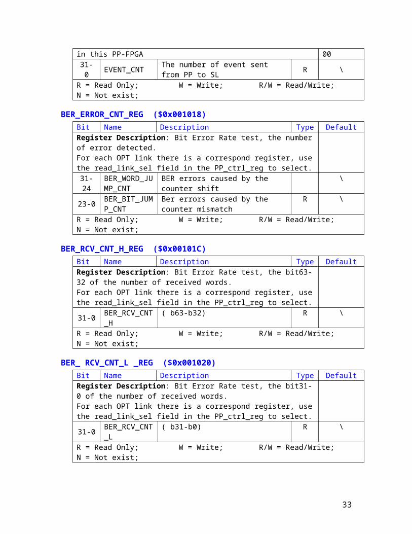
31- 0 EVENT_CNT The number of event sent from PP to SL R \
R = Read Only; W = Write; R/W = Read/Write; N = Not exist;
BER_ERROR_CNT_REG ($0x001018)Bit Name Description Type DefaultRegister Description: Bit Error Rate test, the number of error detected.For each OPT link there is a correspond register, use the read_link_sel field in
25
the PP_ctrl_reg to select.
31-24 BER_WORD_JUMP_CNT
BER errors caused by the counter shift \
23-0 BER_BIT_JUMP_CNT
Ber errors caused by the counter mismatch
R \
R = Read Only; W = Write; R/W = Read/Write; N = Not exist;
BER_RCV_CNT_H_REG ($0x00101C)Bit Name Description Type DefaultRegister Description: Bit Error Rate test, the bit63-32 of the number of received words.For each OPT link there is a correspond register, use the read_link_sel field in the PP_ctrl_reg to select.
31-0 BER_RCV_CNT_H
( b63-b32) R \
R = Read Only; W = Write; R/W = Read/Write; N = Not exist;
BER_ RCV_CNT_L _REG ($0x001020)Bit Name Description Type DefaultRegister Description: Bit Error Rate test, the bit31-0 of the number of received words.For each OPT link there is a correspond register, use the read_link_sel field in the PP_ctrl_reg to select.
31-0 BER_RCV_CNT_L
( b31-b0) R \
R = Read Only; W = Write; R/W = Read/Write; N = Not exist;
MEM_MAX_USAGE_REG0 ($0x001024)Bit Name Description Type DefaultRegister Description: the maximum FIFO usage of bank FIFOs31-29 RESERVE0
28-16 CLUS_DERAN_M_USE
Maximum usage of cluster derandomizer RAM
R \
15-8 CLUS_FIFO_M_USE
maximum usage of cluster bank FIFO R \
7-0 INFO_FIFO_M_USE
maximum usage of information bank FIFO
R \
R = Read Only; W = Write; R/W = Read/Write; N = Not exist;
MEM_MAX_USAGE_REG1 ($0x001028)Bit Name Description Type DefaultRegister Description: the maximum FIFO usage of bank FIFOs.
31-16 RAW_FIFO_M_USE
Maximum usage of RAM bank FIFO \
15-0 ADC_FIFO_M_USE
Maximum usage of ADC value bank FIFO
R \
R = Read Only; W = Write; R/W = Read/Write; N = Not exist;
26
PP_ECS_ERROR_CNT_REG ($0x00102C)Bit Name Description Type DefaultRegister Description: the ECS access error count 0x0000000031- 8 RESERVE0 N7-0 ECS_ERROR_
CNTR \
R = Read Only; W = Write; R/W = Read/Write; N = Not exist;
PP_DERAND_EVNT_CNT_REG ($0x001030) Bit Name Description Type DefaultRegister Description: number of events write into/read from PP derandoridmizer
0x00000000
31-16 OUT_CNT \15-0 IN_CNT R \
R = Read Only; W = Write; R/W = Read/Write; N = Not exist;
PP_DATE_REG ($0x001034)Bit Name Description Type DefaultRegister Description: Automatically generated compilation date of the firmware.
\
31-0 DATE ddmmyyyy R \R = Read Only; W = Write; R/W = Read/Write; N = Not exist;
PP_TIME_REG ($0x001038)Bit Name Description Type DefaultRegister Description: Automatically generated compilation time of the firmware.
\
31-16 Not used R \15-0 TIME hhmm R \
R = Read Only; W = Write; R/W = Read/Write; N = Not exist;
PP_VERSION_REG ($0x00103C)Bit Name Description Type DefaultRegister Description: Frimware release version. \31-16 Reserved23-16 USER_LOGIC_VERSION Firmware version R \15-8 PP_LOGIC_VERSION Firmware version R \7-0 SL_LOGIC_VERSION Firmware version R \
R = Read Only; W = Write; R/W = Read/Write; N = Not exist;
ORX_PROBE_REG ($0x001040)Bit Name Description Type Defa
ultRegister Description: OPT beetle information ( not event based information)For optical links there is a correspond register, use the read_link_sel field in the
27
PP_ctrl_reg to select. Note that each OPT beetle are divided into 4 8bits data stream each correspond to one beetle analog link. Then the 4 8b data stream are separated into even/odd groups.31-24 RESERVE1 0x00
23 OPT_LINK_DISABLE
this link is disabled
22 OPT_CLK_DEAD The opt_clk of this link is not active
21 OPT_EVT_LONGIf there is an event longer than the set event size (eg 35 words), this bit will set and stick.
R
20 OPT_EVT_SHORTIf there is an event shorter than the set event size (eg 35 words), this bit will set and stick.
R
19 SYNCRAM_O_OFLOW
Once there are more than 4 events stored in the syncRAM, this bit is set and stick
18 SYNCRAM_O_UFLOW
Once read event from empty syncRAM, this bit is set and stick
R
17 SYNCRAM_E_OFLOW
Once there are more than 4 events stored in the syncRAM, this bit is set and stick
R
16 SYNCRAM_E_UFLOW
Once read event from empty syncRAM, this bit is set and stick
R
15 TLK_LOS_FLG TLK loss-of-signal flag. (one situation of error)
R
14 TLK_IDLE_FLG TLK receiver idle flag R13 TLK_NORMAL_FLG TLK receiver normal flag12 TLK_CC_FLG TLK Carrier extend flag11 TLK_ERROR_FLG TLK error flag
10-9 RESERVE0 008-0 SYNCRAM_M_USE The maximum used words of the SyncRAM R
R = Read Only; W = Write; R/W = Read/Write; N = Not exist;
ORX_ SYNC_REG ($0x001044)Bit Name Description Type DefaultRegister Description: OPT beetle information (event based information)For each OPT link there is a correspond register, use the read_link_sel field in the PP_ctrl_reg to select. Note that each OPT beetle are divided into 4 8bits data stream each correspond to one beetle analog link. Then the 4 8b data stream are separated into even/odd.
31-28 EVT_LONG_CNT
The number of event longer than 35 R
27-24 EVT_SHORT_CNT
The number of event shorter than 35 R
23-16 SYNCRAM_EVT_W_CNT
The number of Event write into syncRAM R
15-8 SYNCRAM_EVT_O_R_CNT
The number of Event read from odd syncRAM (only for ST)
R
7-0 SYNCRAM_EVT_E_R_CNT
The number of Event read from even syncRAM (for all others but ST this is the only RAM used)
R
28
R = Read Only; W = Write; R/W = Read/Write; N = Not exist;
7.2 User Specific Register
7.2.1 VELO specific registers (starts from 0x002000)
VELO_ADCCLK_PHY_DLY_REGH ($0x002000)Bit Name Description Type DefaultRegister Description: For each ADC channel, an independent phase-adjustable ADC sample clock needs to be generated from the corresponding PP_FPGA. With this register, we can set the detailed Phase Delay for the highest 8 ADC clocks. The phase adjust step is 1/16 of a 40MHz clock and the possible setting value is from 0 to 15.
0x00000000
31- 28 PHY_DLY_7 Set the Phase Delay for ADCClk(15) R/W 0x027- 24 PHY_DLY_6 Set the Phase Delay for ADCClk(14) R/W 0x023- 20 PHY_DLY_5 Set the Phase Delay for ADCClk(13) R/W 0x019- 16 PHY_DLY_4 Set the Phase Delay for ADCClk(12) R/W 0x015- 12 PHY_DLY_3 Set the Phase Delay for ADCClk(11) R/W 0x011- 8 PHY_DLY_2 Set the Phase Delay for ADCClk(10) R/W 0x07- 4 PHY_DLY_1 Set the Phase Delay for ADCClk(9) R/W 0x03- 0 PHY_DLY_0 Set the Phase Delay for ADCClk(8) R/W 0x0
R = Read Only; W = Write; R/W = Read/Write; N = Not exist;
VELO_ADCCLK_PHY_DLY_REGL ($0x002004)Bit Name Description Type DefaultRegister Description: For each ADC channel, an independent phase-adjustable ADC sample clock needs to be generated from the corresponding PP_FPGA. With this register, we can set the detailed Phase Delay for the lowest 8 ADC clocks. The phase adjust step is 1/16 of a 40MHz clock and the possible setting
0x00000000
29
value is from 0 to 15.
31- 28 PHY_DLY_7 Set the Phase Delay for ADCClk(7) R/W 0x027- 24 PHY_DLY_6 Set the Phase Delay for ADCClk(6) R/W 0x023- 20 PHY_DLY_5 Set the Phase Delay for ADCClk(5) R/W 0x019- 16 PHY_DLY_4 Set the Phase Delay for ADCClk(4) R/W 0x015- 12 PHY_DLY_3 Set the Phase Delay for ADCClk(3) R/W 0x011- 8 PHY_DLY_2 Set the Phase Delay for ADCClk(2) R/W 0x07- 4 PHY_DLY_1 Set the Phase Delay for ADCClk(1) R/W 0x03- 0 PHY_DLY_0 Set the Phase Delay for ADCClk(0) R/W 0x0
R = Read Only; W = Write; R/W = Read/Write; N = Not exist;
VELO_ADCCLK_CYC_DLY_REG ($0x002008)Bit Name Description Type DefaultRegister Description: With this register, the Clock Delay can be set for each ADC sample clock. Two bits are used for each channel, and the valid Clock Delay is from 0 to 2 clocks. If the Clock Delay is set to 3, the corresponding channel will be disabled!
0x00000000
31- 30 CYC_DLY_15 Set the Clock Delay for ADCClk(15) R/W 0029- 28 CYC_DLY_14 Set the Clock Delay for ADCClk(14) R/W 00
… … … … …3 – 2 CYC_DLY_1 Set the Clock Delay for ADCClk(1) R/W 001 – 0 CYC_DLY_0 Set the Clock Delay for ADCClk(0) R/W 00
R = Read Only; W = Write; R/W = Read/Write; N = Not exist;
9 CLUS_PARA_REG ($0x00200C, $0x002010 …$0x00202C)Bit Name Description Type DefaultRegister Description: The cluster algorithm needs low threshold and sum threshold for each channel. The ORx has 12 channels thus 12 registers are provided, the ARx will use only 9 of them
0x00004020
31-27 RESERVE026-16 CH_START_S
TRIPThe start strip number of this link(11 bits for velo)
0x00
15-8 STRIP_SUM_THR
Sum threshold R/W 0x40
7-0 STRIP_L_THR Low threshold R/W 0x20R = Read Only; W = Write; R/W = Read/Write; N = Not exist;
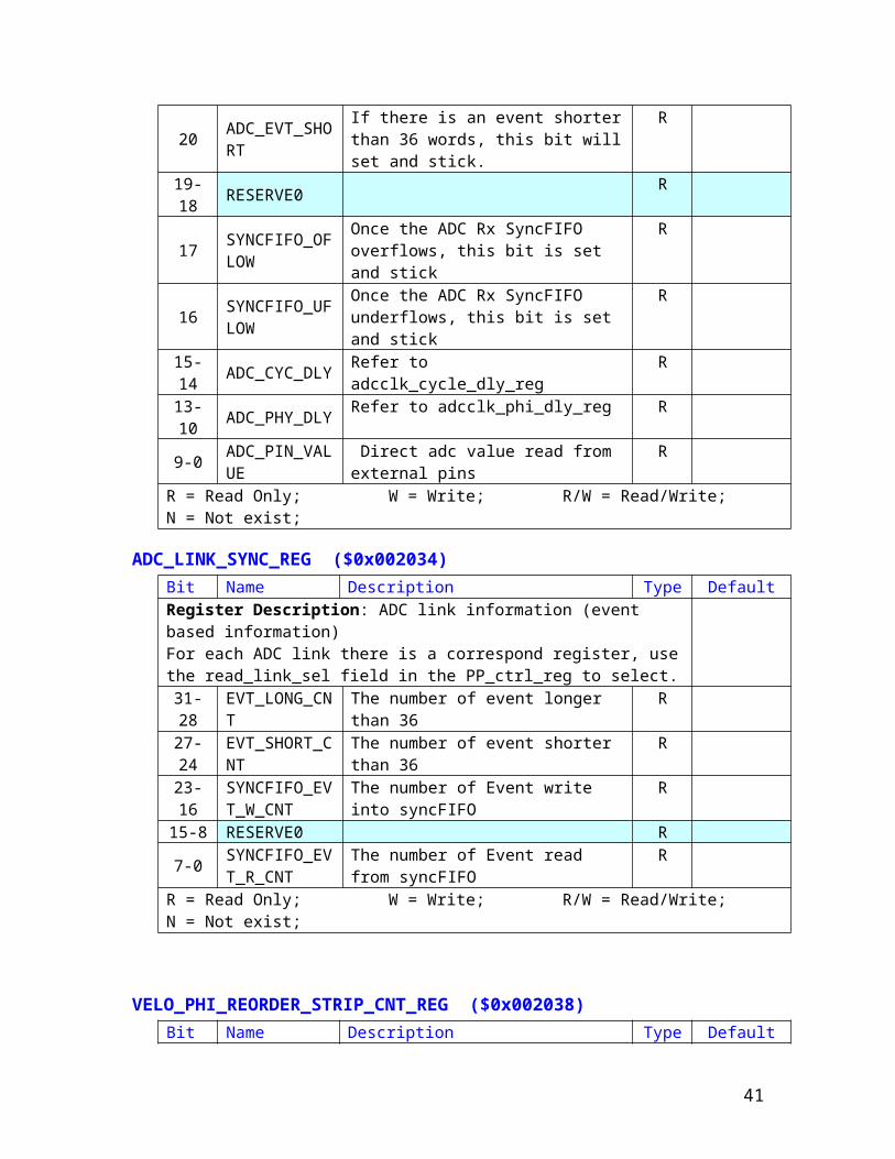
ADC_LINK_PROBE_REG ($0x002030)Bit Name Description Type DefaultRegister Description: ADC link information ( not event based information)For each ADC link there is a correspond register, use the read_link_sel field in the PP_ctrl_reg to select.
31 RESERVE2
30-24 SYNCFIFO_M_USE
The maximum FIFO used word of the SyncFIFO
23-22 RESERVE1 R
21 ADC_EVT_LONG
If there is an event longer than 36 words, this bit will set and stick.
R
30
20 ADC_EVT_SHORT
If there is an event shorter than 36 words, this bit will set and stick.
R
19-18 RESERVE0 R
17 SYNCFIFO_OFLOW
Once the ADC Rx SyncFIFO overflows, this bit is set and stick
R
16 SYNCFIFO_UFLOW
Once the ADC Rx SyncFIFO underflows, this bit is set and stick
R
15-14 ADC_CYC_DLY
Refer to adcclk_cycle_dly_reg R
13-10 ADC_PHY_DLY
Refer to adcclk_phi_dly_reg R
9-0 ADC_PIN_VALUE
Direct adc value read from external pins R
R = Read Only; W = Write; R/W = Read/Write; N = Not exist;
ADC_LINK_SYNC_REG ($0x002034)Bit Name Description Type DefaultRegister Description: ADC link information (event based information)For each ADC link there is a correspond register, use the read_link_sel field in the PP_ctrl_reg to select.
31-28 EVT_LONG_CNT
The number of event longer than 36 R
27-24 EVT_SHORT_CNT
The number of event shorter than 36 R
23-16 SYNCFIFO_EVT_W_CNT
The number of Event write into syncFIFO R
15-8 RESERVE0 R
7-0 SYNCFIFO_EVT_R_CNT
The number of Event read from syncFIFO R
R = Read Only; W = Write; R/W = Read/Write; N = Not exist;
VELO_PHI_REORDER_STRIP_CNT_REG ($0x002038)Bit Name Description Type DefaultRegister Description: The reordering needs some initial values to distinguish between PPs. These values are very difficult to obtain and should be changed only after careful considerations.
0x155AAAD6
31-30 Reserved R/W 0x0
29-24 Constant(4) Number of outer strips in O_RAM(6) for proc(4)
R/W 0x15
23-18 Constant(3) Number of outer strips in O_RAM(6) for proc(3)
R/W 0x16
17-12 Constant(2) Number of outer strips in O_RAM(7) R/W 0x2a
11-6 Constant(1) Sum of the number of inner strips in I_RAM(6) + I_RAM(7)
R/W 0x2b
5-0 Constant(0) Number of inner strips in I_RAM(7) R/W 0x16R = Read Only; W = Write; R/W = Read/Write; N = Not exist;
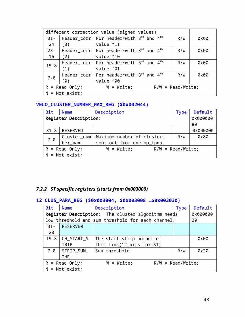
31
VELO_HEADER_CORRECTION_VALUE_STRIP_O_REG ($0x00203C)Bit Name Description Type DefaultRegister Description: Correction constants for strip 0 that is transmitted just after the Beetle header. Each combination of header bits results in a different correction value (signed values)
0x00000000
31-24 Header_corr(3) For header with 3rd and 4th value “11” R/W 0x0023-16 Header_corr(2) For header with 3rd and 4th value “10” R/W 0x0015-8 Header_corr(1) For header with 3rd and 4th value “01” R/W 0x007-0 Header_corr(0) For header with 3rd and 4th value “00” R/W 0x00
R = Read Only; W = Write; R/W = Read/Write; N = Not exist;
VELO_HEADER_CORRECTION_VALUE_STRIP_1_REG ($0x002040)Bit Name Description Type DefaultRegister Description: Correction constants for strip 1 that is transmitted just after the Beetle header. Each combination of header bits results in a different correction value (signed values)
0x00000000
31-24 Header_corr(3) For header with 3rd and 4th value “11” R/W 0x0023-16 Header_corr(2) For header with 3rd and 4th value “10” R/W 0x0015-8 Header_corr(1) For header with 3rd and 4th value “01” R/W 0x007-0 Header_corr(0) For header with 3rd and 4th value “00” R/W 0x00
R = Read Only; W = Write; R/W = Read/Write; N = Not exist;
VELO_CLUSTER_NUMBER_MAX_REG ($0x002044)Bit Name Description Type DefaultRegister Description: 0x0000008031-8 RESERVED 0x000000
7-0 Cluster_number_max
Maximum number of clusters sent out from one pp_fpga.
R/W 0x80
R = Read Only; W = Write; R/W = Read/Write; N = Not exist;
7.2.2 ST specific registers (starts from 0x003000)
12 CLUS_PARA_REG ($0x003004, $0x003008 …$0x003030)Bit Name Description Type DefaultRegister Description: The cluster algorithm needs low threshold and sum threshold for each channel.
0x00000020
31-20 RESERVE019-8 CH_START_S
TRIPThe start strip number of this link(12 bits for ST)
0x00
7-0 STRIP_SUM_THR
Sum threshold R/W 0x20
R = Read Only; W = Write; R/W = Read/Write; N = Not exist;
32
Removed register for optical links, they are common registers now !
ST_HEADER_CORRECTION_VALUE_STRIP_O_REG ($0x00303C)Bit Name Description Type DefaultRegister Description: Correction constants for strip 0 that is transmitted just after the Beetle header. Each combination of header bits results in a different correction value (signed values)
0x00000000
31-24 Header_corr(3) For header with 3rd and 4th value “11” R/W 0x0023-16 Header_corr(2) For header with 3rd and 4th value “10” R/W 0x0015-8 Header_corr(1) For header with 3rd and 4th value “01” R/W 0x007-0 Header_corr(0) For header with 3rd and 4th value “00” R/W 0x00
R = Read Only; W = Write; R/W = Read/Write; N = Not exist;
ST_HEADER_CORRECTION_VALUE_STRIP_1_REG ($0x003040)Bit Name Description Type DefaultRegister Description: Correction constants for strip 1 that is transmitted just after the Beetle header. Each combination of header bits results in a different correction value (signed values)
0x00000000
31-24 Header_corr(3) For header with 3rd and 4th value “11” R/W 0x0023-16 Header_corr(2) For header with 3rd and 4th value “10” R/W 0x0015-8 Header_corr(1) For header with 3rd and 4th value “01” R/W 0x007-0 Header_corr(0) For header with 3rd and 4th value “00” R/W 0x00
R = Read Only; W = Write; R/W = Read/Write; N = Not exist;
ST_CLUSTER_NUMBER_MAX_REG ($0x003044)Bit Name Description Type DefaultRegister Description: 0x0000008031-8 RESERVED 0x000000
7-0 Cluster_number_max
Maximum number of clusters sent out from one pp_fpga.
R/W 0x80
R = Read Only; W = Write; R/W = Read/Write; N = Not exist;
7.2.3 OT specific registers (starts from 0x000480)
7.2.4 CAL specific registers (starts from 0x0004C0)
7.2.5 MUON specific registers (starts from 0x000500)
7.3 Common RAM blocks
DATA_GEN_RAM SectionA (Address range: 0x100000 – 0x1001FF)Word Name Description Type DefaultRAM Description: For ST: On chip data generator RAM located in the input synchronizer, 32-bit wide and 128-word depth.
E:\hdl\vhdl_sim_data\
33
For VELO: On chip data generator RAM located in the input synchronizer, 32-bit wide and 128-word depth.
memory_ini\data_gen_ini.hex
0- 35 GEN_DATA event data(for ST, it is (0-71)) R/W36-127
Reserved Reserved (for ST, it is (72-127)) R/W
R = Read Only; W = Write; R/W = Read/Write; N = Not exist;
DATA_GEN_RAM SectionB (Address range: 0x102000 – 0x1021FF)Word Name Description Type DefaultRAM Description: For ST: On chip data generator RAM located in the input synchronizer, 32-bit wide and 128-word depth.For VELO: On chip data generator RAM located in the input synchronizer, 32-bit wide and 128-word depth.
E:\hdl\vhdl_sim_data\memory_ini\data_gen_ini.hex
0- 35 GEN_DATA event data(for ST, it is (0-71)) R/W36-127
Reserved Reserved (for ST, it is (72-127)) R/W
R = Read Only; W = Write; R/W = Read/Write; N = Not exist;
DATA_GEN_RAM SectionC (Address range: 0x104000 – 0x1041FF)Word Name Description Type DefaultRAM Description: For ST: On chip data generator RAM located in the input synchronizer, 32-bit wide and 128-word depth.For VELO: On chip data generator RAM located in the input synchronizer, 32-bit wide and 128-word depth.
E:\hdl\vhdl_sim_data\memory_ini\data_gen_ini.hex
0- 35 GEN_DATA event data(for ST, it is (0-71)) R/W36-127
Reserved Reserved (for ST, it is (72-127)) R/W
R = Read Only; W = Write; R/W = Read/Write; N = Not exist;
DATA_GEN_RAM SectionD (Address range: 0x106000 – 0x1061FF)Word Name Description Type DefaultRAM Description: For ST: This RAM is reservedFor VELO: On chip data generator RAM located in the input synchronizer, 32-bit wide and 128-word depth.
E:\hdl\vhdl_sim_data\memory_ini\data_gen_in
34
i.hex0- 35 GEN_DATA event data R/W36-127
Reserved Reserved R/W
R = Read Only; W = Write; R/W = Read/Write; N = Not exist;
DATA_GEN_RAM SectionE (Address range: 0x108000 – 0x1081FF)Word Name Description Type DefaultRAM Description: For ST: This RAM is reservedFor VELO: On chip data generator RAM located in the input synchronizer, 32-bit wide and 128-word depth.
E:\hdl\vhdl_sim_data\memory_ini\data_gen_ini.hex
0- 35 GEN_DATA event data R/W36-127
Reserved Reserved R/W
R = Read Only; W = Write; R/W = Read/Write; N = Not exist;
DATA_GEN_RAM SectionF (Address range: 0x10A000 – 0x10A1FF)Word Name Description Type DefaultRAM Description: For ST: This RAM is reservedFor VELO: On chip data generator RAM located in the input synchronizer, 32-bit wide and 128-word depth.
E:\hdl\vhdl_sim_data\memory_ini\data_gen_ini.hex
0- 35 GEN_DATA event data R/W36-127
Reserved Reserved R/W
R = Read Only; W = Write; R/W = Read/Write; N = Not exist;
The three sections of data generator RAM are capable of generating a whole event. They are organized the same way as un-zero suppressed data format.
Word Name Description Type DefaultRAM Description: To set the PEDESTAL value for pedestal sum RAM block, only PEDESTAL(19:10) is significant which will be subtracted from the INPUT DATA (an option to automatically update the pedestal values is given in auto_pedesal_update. A running average over 10-bit is calculated. This RAM block is 32-bit wide and 64-word depth.
pedestal_sum_ram_init.hex
0-63 Pedestal_Sum Corresponding with 64 detector channels 0-31 correspond to the even channels, 32 to 63 to the odd channels
R/W
R = Read Only; W = Write; R/W = Read/Write; N = Not exist;
--ram26Word Name Description Type DefaultRAM Description: Histogram of the first iteration average in LCMS algorithm, for each 32 strip cms one histogram space of 64 words is reserved64x18word
Histo Counters Average histogram R/W
R = Read Only; W = Write; R/W = Read/Write; N = Not exist;
--ram28Word Name Description Type DefaultRAM Description: Histogram of the first iteration slope in LCMS algorithm, for each 32 strip cms one histogram space of 64 words is reserved64x18word
Histo Counters Slope histogram R/W
R = Read Only; W = Write; R/W = Read/Write; N = Not exist;
Word Name Description Type DefaultRAM Description: To set the PEDESTAL value for pedestal sum RAM block, only PEDESTAL(17:10) is significant which will be subtracted from the INPUT DATA (an option to automatically update the pedestal values is given in auto_pedesal_update. A running average over 10-bit is calculated. This RAM block is 32-bit wide and 64-word depth.
pedestal_sum_ram_init.hex
0-63 Pedestal_Sum Corresponding with 64 detector channels 0-31 correspond to the even channels, 32 to 63 to the odd channels
R/W
R = Read Only; W = Write; R/W = Read/Write; N = Not exist;
--ram36Word Name Description Type DefaultRAM Description: Histogram of the first iteration average in LCMS algorithm, for each 32 strip cms one histogram space of 64 words is reserved64x24word
Histo Counters Average histogramSize is 1536 word = 6144 byte
R/W
R = Read Only; W = Write; R/W = Read/Write; N = Not exist;
--ram38Word Name Description Type DefaultRAM Description: Histogram of the second iteration slope in LCMS algorithm, for each 32 strip cms one histogram space of 64 words is reserved64x24word
Histo Counters Slope histogramSize is 1536 word = 6144 byte
R/W
39
R = Read Only; W = Write; R/W = Read/Write; N = Not exist;
7.4.3 OT specific RAM (starts from 0x400000)
7.4.4 CAL specific RAM (starts from 0x500000)
7.4.5 MUON specific RAM (starts from 0x600000)
8. Registers and RAM blocks Definition of SyncLink-FPGA
8.1 Common Registers
A: control registers
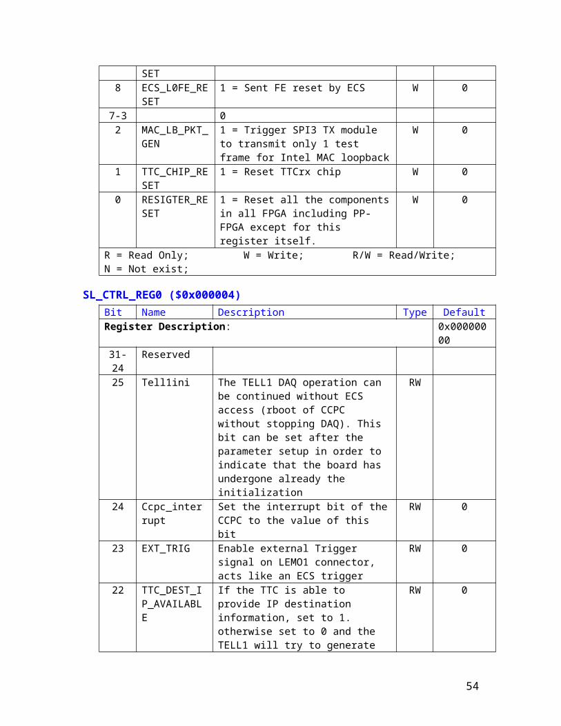
SL_RESET_REG ($0x000000)Bit Name Description Type DefaultRegister Description: Register Description One cycle@40MHz after written, the register will return to its default value. Used to generate pulses
0x00000000
31- 16 N15-13 RESERVE1
12 ECS_TRIGGER_START
1 = Start the ecs trigger sequence programmed by the register ECS_ TRIGGER_NUMBEr _REG and ECS_TRIGGER_SCHEDULE_REG. ECS trigger!
W 0
11 ECS_MEP_FLUSH
Flush the current mep
10 ECS_EVCNT_RESET
Reset the event coutner
9 ECS_BCNT_RESET
Reset the bunch counter
8 ECS_L0FE_RESET
1 = Sent FE reset by ECS W 0
7-3 02 MAC_LB_PKT
_GEN1 = Trigger SPI3 TX module to transmit only 1 test frame for Intel MAC loopback
W 0
1 TTC_CHIP_RESET
1 = Reset TTCrx chip W 0
0 RESIGTER_RESET
1 = Reset all the components in all FPGA including PP-FPGA except for this register itself.
W 0
R = Read Only; W = Write; R/W = Read/Write; N = Not exist;
SL_CTRL_REG0 ($0x000004)Bit Name Description Type Default
40
Register Description: 0x0000000031-24 Reserved
25 Tell1ini The TELL1 DAQ operation can be continued without ECS access (rboot of CCPC without stopping DAQ). This bit can be set after the parameter setup in order to indicate that the board has undergone already the initialization
RW
24 Ccpc_interrupt Set the interrupt bit of the CCPC to the value of this bit
RW 0
23 EXT_TRIG Enable external Trigger signal on LEMO1 connector, acts like an ECS trigger
RW 0
22 TTC_DEST_IP_AVAILABLE
If the TTC is able to provide IP destination information, set to 1. otherwise set to 0 and the TELL1 will try to generate the information by itself
RW 0
21 TTC_TRIGGER_TYPE_AVAILABLE
If the TTC is able to provide trig_type information, set to 1. otherwise set to 0 and the TELL1 will try to generate the trig type information by itself
RW 0
20 TTC_INFO_EN 1 = enables the information sent from TTC (trigger, trigger_type and dest_IP)0 = used the information from ECS_simu
RW 0
19 GBE_ID_WP Write protect for GBE ID PROM18-16 CCPC_PROCE
SS_CTRLTo pause/run/kill DAQ processes via console or a new running DAQ process1 -- IDLE2 – Running3 – Pause4 -- Kill
RW
15 SL_INIT_DONE
Comes from a pin of SyncLink FPGA that indicates this FPGA has been initialized.
R \
14 PP3_INIT_DONE
Comes from a pin of PP0 FPGA that indicates this FPGA has been initialized.
R \
13 PP2_INIT_DONE
Comes from a pin of PP0 FPGA that indicates this FPGA has been initialized.
R \
12 PP1_INIT_DONE
Comes from a pin of PP0 FPGA that indicates this FPGA has been initialized.
R \
11 PP0_INIT_DONE
Comes from a pin of PP0 FPGA that indicates this FPGA has been initialized.
R \
10 ECS_CNT_FREEZE
To freeze certain ecs counters. RW 0
9-8 READ_PP_SEL
The monitor registers for each PP_FPGA share the same ECS address; this field is used to select a certain PP’s register to read out. (0-3)
RW 0
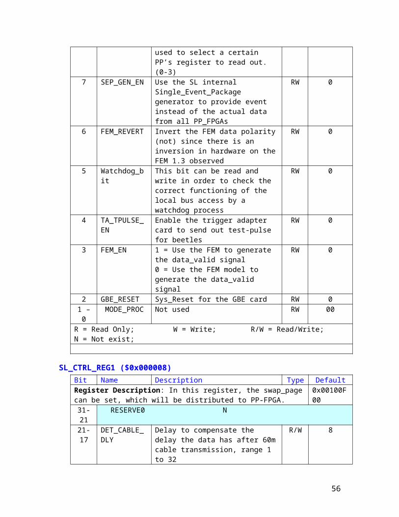
7 SEP_GEN_EN Use the SL internal Single_Event_Package generator to provide event instead of the actual data from all PP_FPGAs
RW 0
41
6 FEM_REVERT Invert the FEM data polarity (not) since there is an inversion in hardware on the FEM 1.3 observed
RW 0
5 Watchdog_bit This bit can be read and write in order to check the correct functioning of the local bus access by a watchdog process
RW 0
4 TA_TPULSE_EN
Enable the trigger adapter card to send out test-pulse for beetles
RW 0
3 FEM_EN 1 = Use the FEM to generate the data_valid signal 0 = Use the FEM model to generate the data_valid signal
RW 0
2 GBE_RESET Sys_Reset for the GBE card RW 01 – 0 MODE_PROC Not used RW 00
R = Read Only; W = Write; R/W = Read/Write; N = Not exist;
SL_CTRL_REG1 ($0x000008)Bit Name Description Type DefaultRegister Description: In this register, the swap_page can be set, which will be distributed to PP-FPGA.
0x00100F00
31- 21 RESERVE0 N21-17 DET_CABLE_
DLYDelay to compensate the delay the data has after 60m cable transmission, range 1 to 32
R/W 8
16- 8 TA_TP_LATANCY
The latency between test pulse and trigger send from the Trigger Adapter (in half clock cycles). The fine delay is set via PLL reconfiguration settings (reg ST_TP_REG)9-bit!
R/W 0xF
7- 0 Swap_page Swap page for accessing external memories.
R/W 0x00
R = Read Only; W = Write; R/W = Read/Write; N = Not exist;
SL_SIMU_CTRL_REG ($0x00000C)Bit Name Description Type DefaultRegister Description: the configuration for the TELL1 supported simulation mode like: trigger adapter control, ECS trigger information.
0x00006440
31-22 RESERVED 0000000021-20 L0-EvCnt(1..0) Two LSBs of L0-EvCnt R/W 0x019-8 ECS_DEST_IP The destination IP address for ecs trigger
The 12 bit are split in two parts 6 bit each for the lowest two octets in the MAC address
0x64
7- 3 ECS_MEP_FACTOR
The number of SEP in each MEP If using the trigger information from ECS.
R/W 4
2- 0 ECS_TRIGGER_TYPE
The type of ecs trigger R/W 0
42
R = Read Only; W = Write; R/W = Read/Write; N = Not exist;
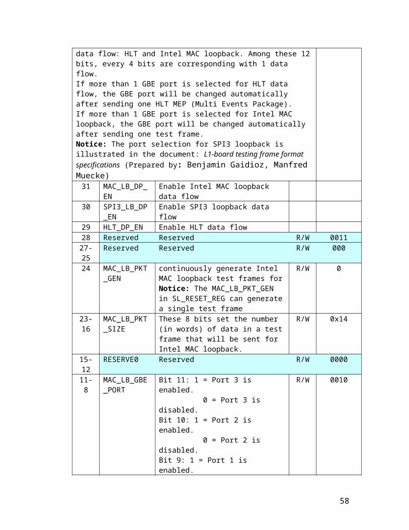
SPI3_TX_CTRL_REG ($0x000010)Bit Name Description Type DefaultRegister Description: This register is used to control the behavior of SPI3 TX module. The lowest 12 bits are used to select GBE port for now 2 kinds of data flow: HLT and Intel MAC loopback. Among these 12 bits, every 4 bits are corresponding with 1 data flow. If more than 1 GBE port is selected for HLT data flow, the GBE port will be changed automatically after sending one HLT MEP (Multi Events Package).If more than 1 GBE port is selected for Intel MAC loopback, the GBE port will be changed automatically after sending one test frame.Notice: The port selection for SPI3 loopback is illustrated in the document: L1-board testing frame format specifications (Prepared by: Benjamin Gaidioz, Manfred Muecke)
0x30140222
31 MAC_LB_DP_EN
Enable Intel MAC loopback data flow
30 SPI3_LB_DP_EN
Enable SPI3 loopback data flow
29 HLT_DP_EN Enable HLT data flow28 Reserved Reserved R/W 0011
27- 25 Reserved Reserved R/W 00024 MAC_LB_PKT
_GENcontinuously generate Intel MAC loopback test frames forNotice: The MAC_LB_PKT_GEN in SL_RESET_REG can generate a single test frame
R/W 0
23- 16 MAC_LB_PKT_SIZE
These 8 bits set the number (in words) of data in a test frame that will be sent for Intel MAC loopback.
R/W 0x14
15- 12 RESERVE0 Reserved R/W 000011- 8 MAC_LB_GBE
_PORTBit 11: 1 = Port 3 is enabled. 0 = Port 3 is disabled.Bit 10: 1 = Port 2 is enabled. 0 = Port 2 is disabled.Bit 9: 1 = Port 1 is enabled. 0 = Port 1 is disabled.Bit 8: 1 = Port 0 is enabled. 0 = Port 0 is disabled.
R/W 0010
7- 4 HLT_GBE_PORT
Bit 7: 1 = Port 3 is enabled. 0 = Port 3 is disabled.Bit 6: 1 = Port 2 is enabled. 0 = Port 2 is disabled.Bit 5: 1 = Port 1 is enabled. 0 = Port 1 is disabled.Bit 4: 1 = Port 0 is enabled. 0 = Port 0 is disabled.
R/W 0010
3- 0 Reserved Reserved R/W 0010R = Read Only; W = Write; R/W = Read/Write; N = Not exist;
43
SPI3_RX_CTRL_REG ($0x000014)Bit Name Description Type DefaultRegister Description: This register is used to control the behavior of SPI3 RX module.
0x00000004
31- 8 RESERVE0 Reserved N \7- 0 LB_PKT_PRO
TOCOLThese 8 bits are used to check whether the received frame is a GBE test frame or not. If not, the received frame will be ignored.
R/W 0x04
R = Read Only; W = Write; R/W = Read/Write; N = Not exist;
THRO_CTRL_REG ($0x000018)Bit Name Description Type DefaultRegister Description: This is L0 board throttle control & status register. It will process 4 PPx_L0_throttle signals coming from 4 PP-FPGA to generate a final L0_throttle signal.
0x07000009
31 SL_THRO Throttle from MEP buffer R \30 PP3_THRO Throttle from cluster_derandomizer R29 PP2_THRO Throttle from cluster_derandomizer R28 PP1_THRO Throttle from cluster_derandomizer R \27 PP0_THRO Throttle from cluster_derandomizer R \
26-8 MEP_USE_THR Threshold for MEP buffer R/W 0x700007-4 RESERVE03 THRO_CNT_EN 1 = enable the throttle counter R/W 12 THRO_CNT_CLR 1 = Clear (see register below) R/W 01 THRO_SIMU_GEN To fake a throttle (works also with
en=0R/W 0
0 THRO_EN 1 = Enable the throttle source R/W 1R = Read Only; W = Write; R/W = Read/Write; N = Not exist;
THRO_CNT_REG ($0x00001C)Bit Name Description Type DefaultRegister Description: By reading this register, we can obtain the current value of L0_Board_Throttle Counter, whose behavior can be controlled by L0_BOARD_THROTTLE_CTRL_REG. When the counter is in running mode (L0_BOARD_THROTTLE_CTRL_REG has its defaulted value), asserted l0_board_throttle_int will make the counter increase at the frequency of 40Mhz. Remark that the counter is saturating (no overflow), 16-bit width.
\
31- 16 RESERVE0 Reserved N \15- 0 THRO_CNT The value of L0_BOARD_throttle
CounterR \
R = Read Only; W = Write; R/W = Read/Write; N = Not exist;
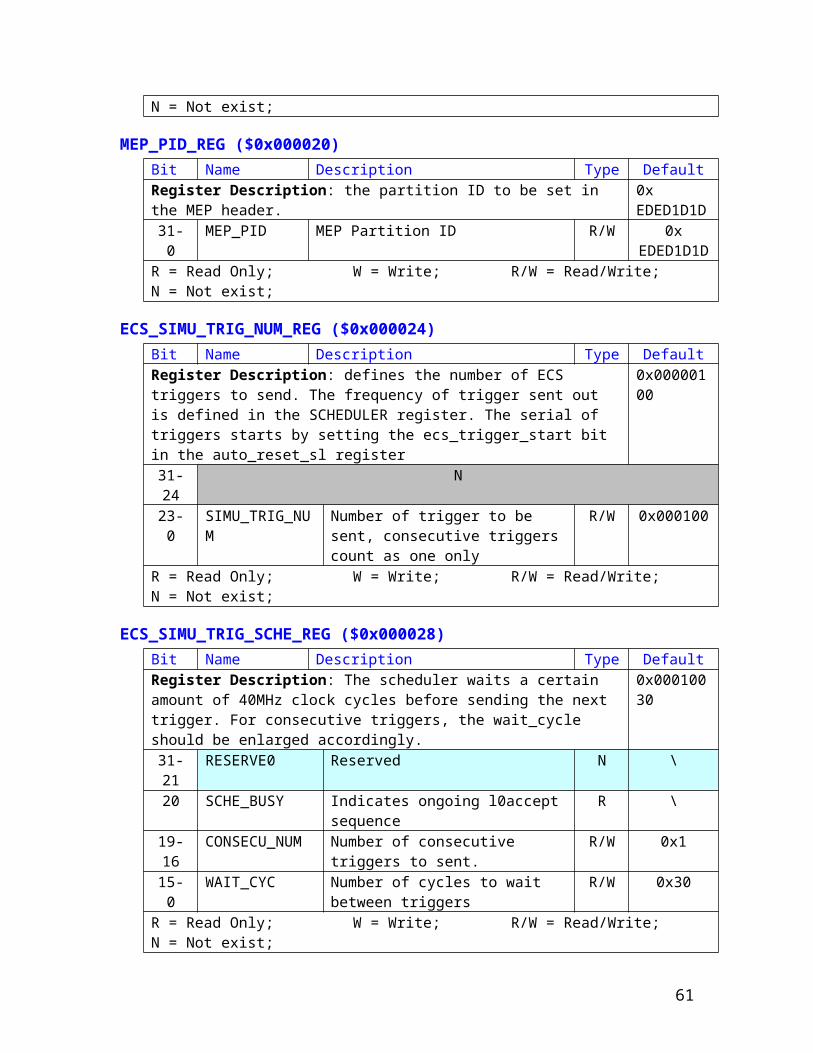
MEP_PID_REG ($0x000020)Bit Name Description Type DefaultRegister Description: the partition ID to be set in the MEP header. 0x
EDED1D1D31- 0 MEP_PID MEP Partition ID R/W 0x
EDED1D1D
44
R = Read Only; W = Write; R/W = Read/Write; N = Not exist;
ECS_SIMU_TRIG_NUM_REG ($0x000024)Bit Name Description Type DefaultRegister Description: defines the number of ECS triggers to send. The frequency of trigger sent out is defined in the SCHEDULER register. The serial of triggers starts by setting the ecs_trigger_start bit in the auto_reset_sl register
0x00000100
31- 24 N23- 0 SIMU_TRIG_NU
MNumber of trigger to be sent, consecutive triggers count as one only
R/W 0x000100
R = Read Only; W = Write; R/W = Read/Write; N = Not exist;
ECS_SIMU_TRIG_SCHE_REG ($0x000028)Bit Name Description Type DefaultRegister Description: The scheduler waits a certain amount of 40MHz clock cycles before sending the next trigger. For consecutive triggers, the wait_cycle should be enlarged accordingly.
0x00010030
31- 21 RESERVE0 Reserved N \20 SCHE_BUSY Indicates ongoing l0accept sequence R \
19-16 CONSECU_NUM Number of consecutive triggers to sent. R/W 0x115- 0 WAIT_CYC Number of cycles to wait between
triggersR/W 0x30
R = Read Only; W = Write; R/W = Read/Write; N = Not exist;
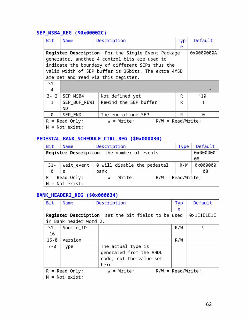
SEP_MSB4_REG ($0x00002C)Bit Name Description Typ
eDefault
Register Description: For the Single Event Package generator, another 4 control bits are used to indicate the boundary of different SEPs thus the valid width of SEP buffer is 36bits. The extra 4MSB are set and read via this register.
0x0000000A
31- 43- 2 SEP_MSB4 Not defined yet R “10”
1 SEP_BUF_REWIND
Rewind the SEP buffer R 1
0 SEP_END The end of one SEP R 0R = Read Only; W = Write; R/W = Read/Write; N = Not exist;
PEDESTAL_BANK_SCHEDULE_CTRL_REG ($0x000030)Bit Name Description Type DefaultRegister Description: the number of events 0x0000000831- 0 Wait_events 0 will disable the pedestal bank R/W 0x00000008
R = Read Only; W = Write; R/W = Read/Write; N = Not exist;
BANK_HEADER2_REG ($0x000034)Bit Name Description Type DefaultRegister Description: set the bit fields to be used in Bank header word 2. 0x1E1E1E1E31- 16 Source_ID R/W \
45
15-8 Version R/W7-0 Type The actual type is generated from the
VHDL code, not the value set hereR = Read Only; W = Write; R/W = Read/Write; N = Not exist;
SL_TP_REG ($0x000038)Bit Name Description Type DefaultRegister Description: set PLL_reconfig module to adjust testpulse delay phase.
0x00000000
31-20 RESERVED \19 READ_PARA Cmd to read data out W18 WRITE_PARA Cmd to write data for phase reconfig W17 RECONFIG Cmd to reconfig PLL W16 Reserved W15 Reserved \
14-12 CNT_PARA PLL counter selection to reconfig W11-8 CNT_TYPE PLL counter type to reconfig W7-0 DATA_ IO Data interface for configuration W
R = Read Only; W = Write; R/W = Read/Write; N = Notexist;
MTU_SIZE_REG ($0x00003C)Bit Name Description Type DefaultRegister Description: The value set in this register doesn’t exactly correspond to the MTU size. It is in fact the IP payload size which is (MTU-
0x000005C8
46
20 byte) and is 1480 for standard Ethernet. The value set in this register must be a multiple of 8. Change this value to achieve Jumbo frames. 31- 16 Reserved R/W 0x000015-0 MTU_size Maximum Ethernet packet size R/W 0x05C8
R = Read Only; W = Write; R/W = Read/Write; N = Not exist;
BANK_CLASS_REG ($0x000040)Bit Name Description Type DefaultRegister Description: The allows to set the bank class (sometimes also called bank type) for each bank. Four different banks are supported and therefore 4 x 8-bit are required.
0x04030201
31- 24 Error class Bank class value for Error bank R/W 0x0423- 16 Pedestal class Bank class value for Pedestal bank R/W 0x0315- 8 nZS class Bank class value for non-zero
suppressed bankR/W 0x02
7- 0 ZS class Bank class value for zero-suppressed bank
R/W 0x01
R = Read Only; W = Write; R/W = Read/Write; N = Not exist;
B: Monitor registers
SL_PP_PROB_REG ($0x001000) Bit Name Description Type DefaultRegister Description: Probe register for each PP_FPGA, Use the read_pp_sle field to choose from 4 PP_FPGAs.
\
31-11 BANK_CNT The number of banks received from correspond PP_FPGA
10-0 SYNCFIFO_M_USE
The maximum usage of the input FIFO for the correspond PP_FPGA
R \
R = Read Only; W = Write; R/W = Read/Write; N = Not exist;
SL_EVT_IN_CNT_REG ($0x001004)Bit Name Description Type DefaultRegister Description: the number of events received from each PP_FPGA. Use the read_pp_sle field to choose from 4 PP_FPGAs.
\
31-0 EVT_IN_CNT Event number from each PP_FPGA R \R = Read Only; W = Write; R/W = Read/Write; N = Not exist;
SL_EVT_OUT_CNT_REG ($0x001008)Bit Name Description Type DefaultRegister Description: the number of events assembled in SyncLink_FPGA \31-0 EVT_OUT_CNT Event assembled in SyncLink R \
R = Read Only; W = Write; R/W = Read/Write; N = Not exist;
Reg 3 is not used now
47
SPI3_TX_MEP_CNT_REG ($0x001010)Bit Name Description Type DefaultRegister Description: This is a counter that counts the number of MEPs transmitted to the GBE TX interface. It is a 32-bit counter and used for debugging purpose.
\
31-0 TX_MEP_CNT SPI MEP counter R \R = Read Only; W = Write; R/W = Read/Write; N = Not exist;
SPI3_TX_WORD_CNT_REG ($0x001014)Bit Name Description Type DefaultRegister Description: This is a counter that counts the number of words in the last MEP transmitted to the GBE TX interface. It is reset up on a new MEP is transmitted. It is a 16-bit counter and used for debugging purpose.
\
31-16 Reserved Reserved R 0x000015-0 TX_WORD_CNT SPI MEP word counter R \
R = Read Only; W = Write; R/W = Read/Write; N = Not exist;
SPI3_TX_SOP_CNT_REG ($0x001018)Bit Name Description Type DefaultRegister Description: This is a counter that counts the number of Start Of Packets (SOP) sent to the GBE TX interface. It is a 32-bit counter and used for debugging purpose.
\
31-0 TX_SOP_CNT SPI SOP counter R \R = Read Only; W = Write; R/W = Read/Write; N = Not exist;
SPI3_TX_EOP_CNT_REG ($0x00101C)Bit Name Description Type DefaultRegister Description: This is a counter that counts the number of End Of Packets (EOP) sent to the GBE TX interface. It is a 32-bit counter and used for debugging purpose.
\
31-0 TX_EOP_CNT SPI EOP counter R \R = Read Only; W = Write; R/W = Read/Write; N = Not exist;
TTC_TRIG_CNT_REG ($0x001020)Bit Name Description Type DefaultRegister Description: The number of TTC triggers \31-0 TRIG_CNT TTC trigger number R \
R = Read Only; W = Write; R/W = Read/Write; N = Not exist;
TTC_TRIG_TYPE_CNT_REG ($0x001024)Bit Name Description Type DefaultRegister Description: The number of TTC triggers types sent \31-0 TRIG_TYPE_CN
TThe number of TTC trigger types sent via TTC system
R \
R = Read Only; W = Write; R/W = Read/Write; N = Not exist;
48
TTC_DEST_IP_CNT_REG ($0x001028)Bit Name Description Type DefaultRegister Description: The number of Destination IP address send via TTC \31-0 DEST_IP_CNT Number of TTC Dest IP R \
R = Read Only; W = Write; R/W = Read/Write; N = Not exist;
TTC_RESET_SIG_CNT_REG ($0x00102C)Bit Name Description Type DefaultRegister Description: The number of all kinds of reset signals send via TTC \31-24 MEP_FLUSH_C
NT number of mep_flush send from TTC R
23-16 L0FE_RESET_CNT
Number of l0fe_reset send from TTC R
15-8 EVCNT_RESET_CNT
Number of event count reset from TTC R
7-0 BCNT_RESET_CNT
Number of bunch count reset from TTC R \
R = Read Only; W = Write; R/W = Read/Write; N = Not exist;
SL_TRIG_CNT_REG ($0x001030)Bit Name Description Type DefaultRegister Description: The number of triggers. ( include TTC and ECS triggers) \31-0 TRIG_CNT Number of triggers R \
R = Read Only; W = Write; R/W = Read/Write; N = Not exist;
TRIG_INFO_TX_CNT_REG ($0x001034)Bit Name Description Type DefaultRegister Description: The number of trigger information send from SyncLink \31-0 TRIG_INFO_TX_
CNTR \
R = Read Only; W = Write; R/W = Read/Write; N = Not exist;
TRIG_INFO_REQ_CNT_REG ($0x001038)Bit Name Description Type DefaultRegister Description: The number of trigger information request from each PP_FPGA. The four PP_FPGA share the same register, use the read_pp_sel to select. Any request from any PP will activate a trigger_info broadcast and requests from other PPs during this period is blocked thus the req_cnt between PPs can be different. On the other hand there is possibility that when the request arrives the TTC trigger type is not arrive yet, and then the request will be omitted. Thus the info_req_cnt can be different from the info_tx_cnt.
\
31-0 TRIG_INFO_REQ_CNT
R \
R = Read Only; W = Write; R/W = Read/Write; N = Not exist;
TRIG_INFO_FIFO_MON_REG0 ($0x00103C)Bit Name Description Type DefaultRegister Description: The trigger information has 5 parts: trigger_type, \
49
trigger_info(bcnt,evcnt..) pcn_cnt, dest_ip and mep_end. They are stored into separated FIFOs. Two registers provide the information about these FIFOs.31-24 PCN_M_USE The maximum used number of the
pcn_fifoR
23-16 EVT_INFO_M_USE
The maximum used number of the event_info_fifo
R
15-8 TRIG_TYPE_M_USE
The maximum used number of the trigger_type_fifo
R \
7-6 Reserved5 PCN_OFLOW Once the pcn_fifo overflows, this bit is
set and stickR
4 PCN_UFLOW Once the pcn_fifo underflows, this bit is set and stick
3 EVT_INFO_OFLOW
Once the Event_info_fifo overflows, this bit is set a stick
2 EVT_INFO_UFLOW
Once the Event_info_fifo underflows, this bit is set and stick
1 TRIG_TYPE_OFLOW
Once the Trigger_type_fifo overflows, this bit is set and stick
R
0 TRIG_TYPE_UFLOW
Once the Trigger_type_fifo underflows, this bit is set and stick
R
7-0 \R = Read Only; W = Write; R/W = Read/Write; N = Not exist;
TRIG_INFO_FIFO_MON_REG1 ($0x001040)Bit Name Description Type DefaultRegister Description: The trigger information has 5 parts: trigger_type, trigger_info(bcnt,evcnt..) pcn_cnt, dest_ip and mep_end. They are stored into separated FIFOs. Two registers provide the information about these FIFOs.
\
31-24 DEST_IP_M_USE
The maximum used number of the dest_ip_fifo
R
23-16 MEP_END_M_USE
The maximum used number of the mep_end_fifo
R
15-43 DEST_IP_OFLO
WOnce the Dest_ip_fifo overflows, this bit is set and stick
2 DEST_IP_UFLOW
Once the Dest_ip_fifo underflows, this bit is set and stick
R
1 MEP_END_OFLOW
Once the mep_end_fifo overflows, this bit is set and stick
R
0 MEP_END_UFLOW
Once the mep_end_fifo underflows, this bit is set and stick
R
R = Read Only; W = Write; R/W = Read/Write; N = Not exist;
MEP_WRITE_CNT_REG ($0x001044)Bit Name Description Type DefaultRegister Description: The number of MEPs written into buffer \31-0 MEP_WRITE_C
NTR \
50
R = Read Only; W = Write; R/W = Read/Write; N = Not exist;
MEP_READ_CNT_REG ($0x001048)Bit Name Description Type DefaultRegister Description: The number of MEPs read out from buffer \31-0 MEP_READ_CN
TR \
R = Read Only; W = Write; R/W = Read/Write; N = Not exist;
MEP_MAX_USAGE_REG ($0x00104C)Bit Name Description Type DefaultRegister Description: The number of MEPs read out from buffer \31-19 Reserve18-0 MEP_MAX_USA
GER \
R = Read Only; W = Write; R/W = Read/Write; N = Not exist;
SL_ERR_LOG_REG ($0x001050)Bit Name Description Type DefaultRegister Description: This is a log register to monitor the flow information of FIFOs used in SL-FPGA, which should be 0 normally.
\
31- 30 Reserved R \29 LEN_FIFO_O_FL
OW_ERROverflow log of LEN fifo used in packet framer of SL
R 0
28 LEN_FIFO_U_FLOW_ERR
Underflow log of LEN fifo used in packet framer of SL
R 0
27 HEADER_FIFO_O_FLOW_ERR
Overflow log of HEADER fifo used in packet framer of SL
R 0
26 HEADER_FIFO_U_FLOW_ERR
Underflow log of HEADER fifo used in packet framer of SL
R 0
25 DATA_FIFO_O_FLOW_ERR
Overflow log of DATA fifo used in packet framer of SL
R 0
24 DATA_FIFO_U_FLOW_ERR
Underflow log of DATA fifo used in packet framer of SL
R 0
23 MEP_INFO_FIFO_O_FLOW_ERR
Overflow log of MEP info fifo used in SL
R 0
22 MEP_INFO_FIFO_U_FLOW_ERR
Underflow log of MEP info fifo used in SL
R 0
21 SEP_LEN_FIFO_O_FLOW_ERR
Overflow log of LEN fifo used in MEP generator of SL
R 0
20 SEP_LEN_FIFO_U_FLOW_ERR
Underflow log of LEN fifo used in MEP generator of SL
R 0
19 SEP_DATA_FIFO_O_FLOW_ERR
Overflow log of DATA fifo used in MEP generator of SL
R 0
18 SEP_DATA_FIFO_U_FLOW_ERR
Underflow log of DATA fifo used in MEP generator of SL
R 0
17 WRITE_EN_WHI Monitor of write activity in the Linker R 0
51
LE_END_OUT_ERR
of SL
16 NORMAL_ERR_BANK_COLLIS_ERR
Monitor of bank assemble activity in the Linker of SL
R 0
15 ERR_INFO_3_FIFO_O_FLOW_ERR
Overflow log of ERROR info fifo 3 used in Linker of SL
R 0
14 ERR_INFO_3_FIFO_U_FLOW_ERR
Underflow log of ERROR info fifo 3 used in Linker of SL
R 0
13 ERR_INFO_2_FIFO_O_FLOW_ERR
Overflow log of ERROR info fifo 2 used in Linker of SL
R 0
12 ERR_INFO_2_FIFO_U_FLOW_ERR
Underflow log of ERROR info fifo 2 used in Linker of SL
R 0
11 ERR_INFO_1_FIFO_O_FLOW_ERR
Overflow log of ERROR info fifo 1 used in Linker of SL
R 0
10 ERR_INFO_1_FIFO_U_FLOW_ERR
Underflow log of ERROR info fifo 1 used in Linker of SL
R 0
9 ERR_INFO_0_FIFO_O_FLOW_ERR
Overflow log of ERROR info fifo 0 used in Linker of SL
R 0
8 ERR_INFO_0_FIFO_U_FLOW_ERR
Underflow log of ERROR info fifo 0 used in Linker of SL
R 0
7 PP3_DATA_FIFO_O_FLOW_ERR
Overflow log of PP3 data fifo used in Linker of SL
R 0
6 PP3_DATA_FIFO_U_FLOW_ERR
Underflow log of PP3 data fifo used in Linker of SL
R 0
5 PP2_DATA_FIFO_O_FLOW_ERR
Overflow log of PP2 data fifo used in Linker of SL
R 0
4 PP2_DATA_FIFO_U_FLOW_ERR
Underflow log of PP2 data fifo used in Linker of SL
R 0
3 PP1_DATA_FIFO_O_FLOW_ERR
Overflow log of PP1 data fifo used in Linker of SL
R 0
2 PP1_DATA_FIFO_U_FLOW_ERR
Underflow log of PP1 data fifo used in Linker of SL
R 0
1 PP0_DATA_FIFO_O_FLOW_ERR
Overflow log of PP0 data fifo used in Linker of SL
R 0
0 PP0_DATA_FIFO_U_FLOW_ERR
Underflow log of PP0 data fifo used in Linker of SL
R 0
R = Read Only; W = Write; R/W = Read/Write; N = Not exist;
SL_MAX_USE_REG ($0x001054)Bit Name Description Type DefaultRegister Description: the maximum FIFO usage of SyncLink internal FIFO \
52
buffers used by SEP linker.31- 28 Reserved R \27-21 SEP_LEN_FIFO_
M_USE 20-10 SEP_DATA_FIF
O_M_USE9- 0 MEP_HEADER_
FIFO_M_USER \
R = Read Only; W = Write; R/W = Read/Write; N = Not exist;
FROZEN_EVID_REG ($0x001058)Bit Name Description Type DefaultRegister Description: when ECS_forzen is set, the L0EvID is latched into this register.
\
31- 0 L0EvID mirror R \R = Read Only; W = Write; R/W = Read/Write; N = Not exist;
FROZEN_BCNT_REG ($0x00105C)Bit Name Description Type DefaultRegister Description: when ECS_forzen is set, the BCnt is latched into this register.accesses to the SL-FPGA.
\
31- 12 Reserved R \11- 0 BCnt mirror Counter value R \
R = Read Only; W = Write; R/W = Read/Write; N = Not exist;
FRAMER_MAX_USE_REG ($0x001060)Bit Name Description Type DefaultRegister Description: the number of MEPs that are bigger than 64K bytes, and the Maximum usage of the FIFOs used by packet framer
\
31-20 MEP_16K_WORD_CNT
19-12 FRAG_DATA_FIFO_MAX_USE
11-5 FRAG_HEADER_FIFO_MAX_USE
4- 0 FRAG_LEN_FIFO_MAX_USE
R \
R = Read Only; W = Write; R/W = Read/Write; N = Not exist;
REAL_RATE_REG0 ($0x001064)Bit Name Description Type DefaultRegister Description: the data rate statistic for GBE SPI3 interface. \31- 20 PP0_RATE The number of valid words from PP0 in
2^12 cycles@120MHz periodR \
19- 0 TRIGGER_RATE The actual trigger number is 2^20 cycles@40MHz period
R \
R = Read Only; W = Write; R/W = Read/Write; N = Not exist;
53
REAL_RATE_REG1 ($0x001068)Bit Name Description Type DefaultRegister Description: The actual rate statistic. \31- 20 PP1_RATE The number of valid words from PP1 in
2^12 cycles@120MHz periodR \
19- 0 SL_LINK_EVENT_RATE
The number of events from SL Linker in 2^20 cycles@120MHz period
R \
R = Read Only; W = Write; R/W = Read/Write; N = Not exist;
REAL_RATE_REG2 ($0x00106C)Bit Name Description Type DefaultRegister Description: The actual rate statistic. \31- 20 PP2_RATE The number of valid words from PP2 in
2^12 cycles@120MHz periodR \
19- 0 MEP_IN_RATE The number of MEPs written into QDR buffer in 2^20 cycles@120MHz period
R \
R = Read Only; W = Write; R/W = Read/Write; N = Not exist;
REAL_RATE_REG3 ($0x001070)Bit Name Description Type DefaultRegister Description: The actual rate statistic. \31- 20 PP3_RATE The number of valid words from PP3 in
2^12 cycles@120MHz periodR \
19- 0 MEP_OUT_RATE
The number of MEPs read out from QDR buffer in 2^20 cycles@120MHz period
R \
R = Read Only; W = Write; R/W = Read/Write; N = Not exist;
REAL_RATE_REG4 ($0x001074)Bit Name Description Type DefaultRegister Description: The actual rate statistic. \31- 16 SL_LINK_RATE The number of words from SL Linker in
65536 cycles@120MHz periodR \
15- 0 SPI3_ RATE The number of words feed into SPI3 interface in 65536 cycles@120MHz period
R \
R = Read Only; W = Write; R/W = Read/Write; N = Not exist;
SL_FLOWCTRL_MONITOR_REG ($0x001078)Bit Name Description Type DefaultRegister Description: This register gives the current and logged(in the past 2us) status of SL flow control signals
R = Read Only; W = Write; R/W = Read/Write; N = Not exist;
MEP_GT_16K_CNT_REG ($0x00107C)Bit Name Description Type DefaultRegister Description: Counter of the MEPs that are bigger than 64kbyte (16kword) and therefore are sent out as empty MEPs
\
31-0 mep_16K_word_cnt 32-bit counter R \R = Read Only; W = Write; R/W = Read/Write; N = Not exist;
SL_DATE_REG ($0x001080)Bit Name Description Type DefaultRegister Description: Automatically generated compilation date of the firmware.
\
31-0 DATE ddmmyyyy R \R = Read Only; W = Write; R/W = Read/Write; N = Not exist;
SL_TIME_REG ($0x001084)Bit Name Description Type DefaultRegister Description: Automatically generated compilation time of the firmware.
\
31-16 Not used R \15-0 TIME hhmm R \
R = Read Only; W = Write; R/W = Read/Write; N = Not exist;
55
SL_VERSION_REG ($0x001088)Bit Name Description Type DefaultRegister Description: Frimware release version. \31-16 Reserved R \15-8 PP_LOGIC_VERSION Firmware version R \7-0 SL_LOGIC_VERSION Firmware version R \
R = Read Only; W = Write; R/W = Read/Write; N = Not exist;
SL_TRIGGER_FIFO_USED_REG0 ($0x00108C)Bit Name Description Type DefaultRegister Description: Frimware release version. \31-24 dest_IP_rdusedw Destination fifo used R \23-16 trigger_type_usedw Trigger type fifo used R \15-8 Pcn_usedw Pcn fifo used R \7-0 Event_info_usedw Event fifo used R \
R = Read Only; W = Write; R/W = Read/Write; N = Not exist;
SL_TRIGGER_FIFO_USED_REG1 ($0x001090)Bit Name Description Type DefaultRegister Description: Frimware release version. \31-8 Reserved R \7-0 Mep_end_rdusedw Mep end fifo used R \
R = Read Only; W = Write; R/W = Read/Write; N = Not exist;
SL_FEM_DV_CNT_REG ($0x001094)Bit Name Description Type DefaultRegister Description: Frimware release version. \31-0 Fem_dv_count Counter for FEM events R \
R = Read Only; W = Write; R/W = Read/Write; N = Not exist;
SL_DEST_IP_L0_EVID_LSB_ERROR_CNT_REG ($0x001098)Bit Name Description Type DefaultRegister Description: Frimware release version. \
31-16 RESERVED15-0 l0evid_lsb_error Counter for errors detected on
wrong evid LSBs transmitted with the TTC long broadcast
R \
56
command used to set the destination ip. This counter will be full for ECS triggers !
R = Read Only; W = Write; R/W = Read/Write; N = Not exist;
8.3 Common RAM blocks
MEP_LOCATION_RAM (Address range: 0x100000 – 0x1001FF) Word Name Description Type DefaultRAM Description: Since the MEP size is variable, it is difficult to distinguish the boundary of MEP if look at the contents of the MEP buffer. The wraparound and overwritten makes it even worse that you can’t start to trace the MEP from the beginning of the MEP buffer. This MEP_location_RAM is a special RAM block used to record the start address of each MEP. When written a MEP into the buffer, the corresponding start address is written into this RAM block. After 128 MEPs, this RAM is overwritten from the beginning thus it can always keep the information of the last 128 MEPs. The 19 LSB is the actual start address of the MEP, the 13 MSB is the MEP id that can be used to verify if it is a valid and correspond MEP at that location.
0-127 Bit 31-19 MEP_ID
The MEP ID R
Bit 18-0MEP_SADDR
The start address of MEP. It is calculated in words. Need to shift 2 bits left and plus the base address of MEP buffer to get the ECS address of that location.
R \
R = Read Only; W = Write; R/W = Read/Write; N = Not exist;
Word Name Description Type DefaultRAM Description: In these two RAM blocks, we can set the IP packet header information for HLT and L1 respectively. The fields in blue are fixed for each TELL1 board and should be set by ECS after reset and kept during the whole run. The other fields in purple are automatically calculated by the TELL1 IP packet framer block during the MEP fragmentation. These unfixed fields must be set proper initial values according to the descriptions below.This RAM is 32-bit width and 32-word depth.
e:\hdl\vhdl_sim_data\memory_ini\ipv4_header.hex
0 DA[47:0] Ethernet destination address: The 38 MSB is set by ECS.The 10 LSB (DA[9..0]) is set by TELL1 IP packet framer, based on information received by the TTC, and thus these bits in the header RAM block should all be set to ‘0’;
R/W1
1 SA[47:0] Ethernet source address R/W2
3TYPE Ethernet type R/WVSERSION/IHL
Version: 4-bit IP version number.IHL: 4-bit Internet Header Length in 32-bit words.
Type of Service
Indication of desired service for this packet.
4 TOTAL_LEN Total length of this packet: set by TELL1 IP packet framer and must be all set to ‘0’ in the header RAM block
R/W
Identification Assembly aid, set by TELL1 IP packet. The MSB (Bit 15) must be set to 1 for L1 and to 0 for HLT. The least significant 15 must be set to all ‘0’ in the header RAM block.
5 FLAG Bit 0: always 0 Bit 1: (DF) 0 = may fragment, 1 = don’t fragment. Must always be set to 0. Bit 2: (MF) 0 = Last fragment, 1 = more fragments. Set by TELL1 IP packet framer and must be set to ‘0’ in the header RAM block.
R/W
Fragment offset
This measures where the fragment belongs in the packet. Set by TELL1 IP packet framer and must be set to all ‘0’ in the header RAM block.
Time to live Time in seconds for the packet to stay in the net: set by ECS.
Protocol Indicates the next level protocol, set by ECS; differs for L1 and HLT.
58
6 Header checksum
The checksum is on the header only: It is the 16 bit one’s complement of the one’s complement sum of all 16 bit words in the IP header. These are the 10 16 bit words starting at the Version / Type of Service field up and including to the IP Destination Address (those fields inside the red box). It is important that for the purpose of this calculation the 16 bit words are assumed to get the most significant byte (of the two bytes) from the lower address (assuming that the bytes are addressed linearly – this is sometimes referred to as big-endian byte ordering). For the calculation of the checksum the checksum field is assumed to be 0. This field in the header RAM block should be set as the pre-calculated sum of the 10 16-bit words with all proper initial value.
R/W
6 IP SA IP source address. Set by ECS. Differs for L1 and HLT.
R/W77 IP DA IP destination address. The higher 22 bits are
assigned by the ECS. The least significant 10 bits are set by TELL1 IP packet framer and must be set to all ‘0’ in the header RAM block.
R/W8
9-31 Reserved Reserved R/WR = Read Only; W = Write; R/W = Read/Write; N = Not exist;
Word Name Description Type DefaultRAM Description: When SPI3 TX module is triggered to send test frame for
59
Intel MAC loopback, it will read the test frame data from this RAM. So the test frame for Intel MAC loopback is defined in this RAM as the above table.In the above table, the read part is Ethernet header, the green part is IP header and the yellow part is test frame header. In order to define a valid test frame for Intel MAC loopback, TYPE must be equal to 0x0800; PROTOCOL must be equal to IPV4_Protocal_for_LPB (defined in SPI3_RX_CTRL_REG); Test_ID must be equal to 0x0003.This RAM is 32-bit width, 256-word depth.
\
0-511 Test Frame Definition
Define test frame for Intel MAC loopback R/W \
R = Read Only; W = Write; R/W = Read/Write; N = Not exist;
INTEL_MAC_LPB_RX_RAM (Address range: 0x106000 – 0x1063FF)Word Name Description Type DefaultRAM Description: When SPI3 RX module receives one test frame from Intel MAC loopback, it will write the test frame into this RAM.This RAM is 32-bit width, 256-word depth. \0-511 Received test
frameSaves the last valid received frame from Intel MAC loopback.
R/W \
R = Read Only; W = Write; R/W = Read/Write; N = Not exist;
SEP_GEN_RAM (Address range: 0x200000 – 0x20FFFF)Word Name Description Type DefaultRAM Description: The Single Event Package Generator is used to generate a pre-defined SEP instead of the actual event linked from the PP_FPGA. It is 36bit wide and 16K words deep. The 4MSB is accessed via a register (SEP_MSB_4B_REG) and used as the control bits for separating SEP. The 32 LSB is the actual data of the SEP.
\
16K words
Bit 35-32 Access via SEP_MSB_4B registerBit 31- 0 SEP data R/W \
R = Read Only; W = Write; R/W = Read/Write; N = Not exist;
8.4 User Specific RAM blocksAt the moment, no user specific RAM blocks are defined.
9. I2C bus address definition
I2C BUS 0 (mixed)Device ADDRESS
Description: Bus used for several devices.TELL1 board ID prom 0x50
60
TTCrx base address 0x58FEM Beetle base address 0x70
The TELL1 board ID is defined to be the following sequence:
Byte 0 (4 MSBs) Sytem (DAQ) 0x1Byte 0 (4 LSBs) Type (TELL1) 0x1Byte 1 Revision (is equal to TELL1
version)Production is 0x04
0x04
Byte 2 MSBs of the serial number 0x00Byte 3 LSBs of the serial number 0xXXByte 4 VHDL-Detector ID 0xXXByte 5 Detector ID 0xXX…Byte 32-… Production test information
Ascii code for TELL1 label information “40DLAUTL000DDD”DDD is the serial ID in decimal
VHDL-Detector ID see register Constant_reg in PP_FPGA:0x1 =VELO, 0x2 =ST, 0x3 =OT, 0x4=CAL, 0x5=MUON, 0x6=L0MUON, 0x7=L0DU0x8= L0PUS, 0x9= RICH
Description: This bus was foreseen to be used to access the FPGAs via I2C as long as there was no CCPC access to these chips. Now this is used for the trigger adapter to control a Beetle connected to the trigger adapter card.Trigger Adapter Beetel Base address eg Lausanne 0x3F
I2C BUS 2 (A-Rx DAC bus)Device ADDRESS
61
Description: Used to set the DACs on the A-Rx cards. Not connected when O-Rx cards are used.DAC PP0 0x54DAC PP1 0x55DAC PP2 0x56DAC PP3 0x57
I2C BUS 3 (GBE Tx card bus)Device ADDRESS
Description: Used for the GBE id prom and the temperature sensors on TELL1.GBE ID prom 0x57Temperature_sens_1 (FPGA PP0) 0x48Temperature_sens_2 (Under GBE card) 0x4A
Appendix: Example codes for C access
1: Register Read/Write
/* example code for read-modify-write ECS registers */ int rmw_ecs_register(void){ u_int32_t err; //Variable for the specific register, which knows the bit structure of this reg PP_CTRL_REG0 ctrl_reg0; //read the register first to have the original setting values err |= lb_read_word(PP_BADDR[0]+PP_CTRL_REG0_ADDR, &ctrl_reg0.All); //modify the bit fields ctrl_reg0.Sepe.DATA_SCALE_MODE = 2; ctrl_reg0.Sepe.DATA_GEN_EN = 1; ctrl_reg0.Sepe.READ_LINK_SEL = 12; ctrl_reg0.Sepe.PSEUDO_BIT_L_THR= 0x80; ctrl_reg0.Sepe.PSEUDO_BIT_H_THR= 0x90; //write back the modified value err |= lb_write_word(PP_BADDR[0]+PP_CTRL_REG0_ADDR, ctrl_reg0.All); return(err);}