76
DEPT .OF. E.C.E, LITS, KHAMMAM DEPARTMENT OF ELECTRONICS & COMMUNICATION ENGINEERING ELECTRONIC DEVICES & CIRCUITS LAB MANUAL II YEAR I SEMESTER (ECE) 0
| Date post: | 22-Dec-2015 |
| Category: |
Documents |
| Upload: | saikrishna |
| View: | 46 times |
| Download: | 1 times |
DEPARTMENT OF ELECTRONICS & COMMUNICATION ENGINEERING
ELECTRONIC DEVICES & CIRCUITS LAB MANUALII YEAR I SEMESTER (ECE)
LAQSHYA INSTITUTE OF TECHNOLOGY AND SCIENCES
TANIKELLA (V), KONIJERLA (M), KHAMMAM
0
ELECTRONIC DEVICES & CIRCUITS LAB MANUAL
II YEAR I SEMESTER (ECE)
1
INDEX
S.NO.
NAME OF THE EXPERIMENT PG.NO.
1 P-N JUNCTION DIODE CHARACTERISTICS 3
2 ZENER DIODE CHARACTERSTICS 7
3 TRANSISTOR COMMON -BASE CONFIGURATION 11
4 TRANSISTOR CE CHARACTERSTICS 15
5 HALF WAVE RECTIFIER 19
6 FULLWAVE RECTIFIER 23
7 FET CHARACTERISTICS 26
8 h-PARAMETERS OF CE CONFIGURATION 30
9 TRANSISTOR CE AMPLIFIER 36
10 COMMON COLLECTOR AMPLIFIER 40
11 COMMON SOURCE FET AMPLIFIER 45
12 SILICON-CONTROLLED RECTIFIER(SCR) CHARACTERISTICS
49
13 UJT CHARACTERISTICS 52
2
Exp No: Date :
1. P-N JUNCTION DIODE CHARACTERISTICS
AIM:-To observe and draw the Forward and Reverse bias V-I Characteristics of a P-N Junction diode.
APPARATUS:-
P-N Diode - IN4007. Regulated Power supply - (0-30v) Resistor - 1KΩ Ammeters - (0-200 mA, 0-500mA) Voltmeter - (0-20 V) Bread board Connecting wires
THEORY:-
A p-n junction diode conducts only in one direction. The V-I characteristics of the diode
are curve between voltage across the diode and current through the diode. When external voltage is zero,
circuit is open and the potential barrier does not allow the current to flow. Therefore, the circuit current
is zero.
When P-type (Anode is connected to +ve terminal and n- type (cathode) is connected to –ve
terminal of the supply voltage, is known as forward bias. The potential barrier is reduced when diode is
in the forward biased condition. At some forward voltage, the potential barrier altogether eliminated
and current starts flowing through the diode and also in the circuit. The diode is said to be in ON state.
The current increases with increasing forward voltage.
When N-type (cathode) is connected to +ve terminal and P-type (Anode) is connected
–ve terminal of the supply voltage is known as reverse bias and the potential barrier across the junction
increases. Therefore, the junction resistance becomes very high and a very small current (reverse
saturation current) flows in the circuit due to minority charge carriers. The diode is said to be in OFF
state.
3
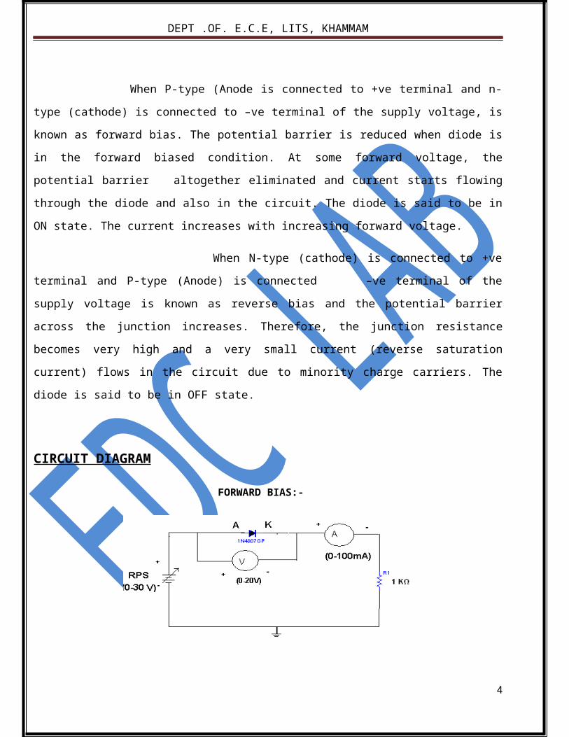
CIRCUIT DIAGRAM
FORWARD BIAS:-
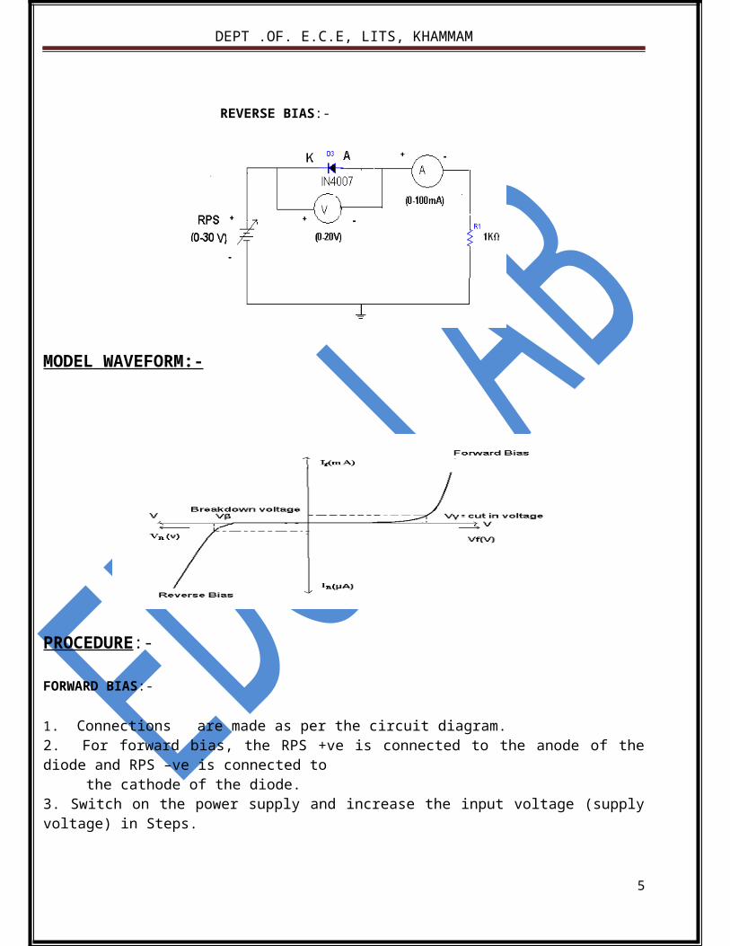
REVERSE BIAS:-
MODEL WAVEFORM:-
4
PROCEDURE:-
FORWARD BIAS:-
1. Connections are made as per the circuit diagram.2. For forward bias, the RPS +ve is connected to the anode of the diode and RPS –ve is connected to the cathode of the diode.3. Switch on the power supply and increase the input voltage (supply voltage) in Steps.4. Note down the corresponding current flowing through the diode and voltage across the diode for each and every step of the input voltage.5. The reading of voltage and current are tabulated.6. Graph is plotted between voltage and current.
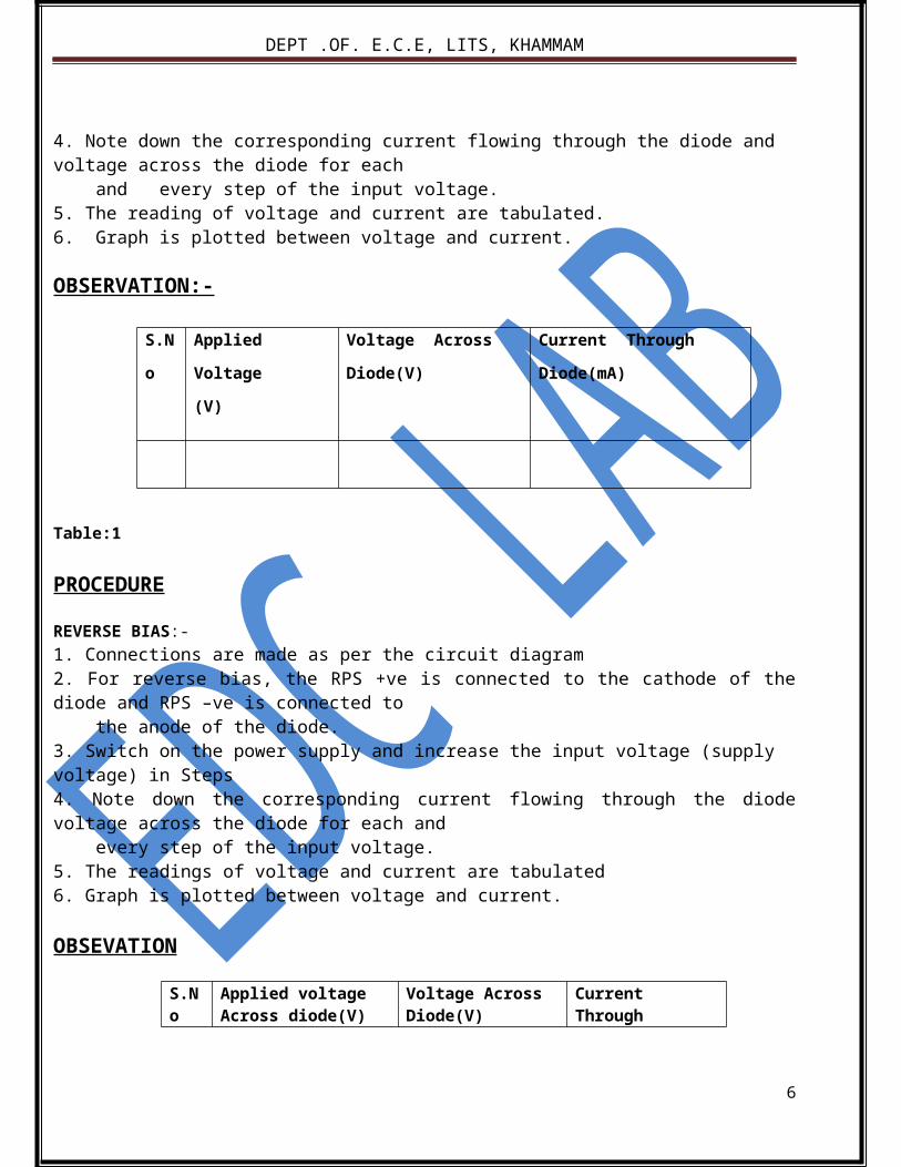
OBSERVATION:-
S.No Applied Voltage
(V)
Voltage Across Diode(V) Current Through
Diode(mA)
Table:1
PROCEDURE
REVERSE BIAS:-1. Connections are made as per the circuit diagram2. For reverse bias, the RPS +ve is connected to the cathode of the diode and RPS –ve is connected to the anode of the diode.3. Switch on the power supply and increase the input voltage (supply voltage) in Steps4. Note down the corresponding current flowing through the diode voltage across the diode for each and every step of the input voltage.5. The readings of voltage and current are tabulated6. Graph is plotted between voltage and current.
OBSEVATION
S.No Applied voltage Across diode(V)
Voltage Across Diode(V)
Current Through Diode(mA)
Table:2
5
PRECAUTIONS
1. All the connections should be correct.2. Parallax error should be avoided while taking the readings from the analog meters.
RESULT: Forward and Reverse Bias characteristics for a p-n diode is observed
VIVA QESTIONS:-
1. Define depletion region of a diode?2. What is meant by transition & space charge capacitance of a diode?3. Is the V-I relationship of a diode Linear or Exponential?4. Define cut-in voltage of a diode and specify the values for Si and Ge diodes?5. What are the applications of a p-n diode? 6. Draw the ideal characteristics of P-N junction diode?7. What is the diode equation?8. What is PIV?9. What is the break down voltage?10. What is the effect of temperature on PN junction diode?
6
Exp No: Date :
2. ZENER DIODE CHARACTERISTICS
AIM: - a) To observe and draw the static characteristics of a zener diode
b) To find the voltage regulation of a given zener diode
APPARATUS: -
Zener diode - 1N4735A
Regulated Power Supply - (0-30v).
Voltmeter - (0-20v)
Ammeter - (0-100mA)
Resistor - (1KOhm)
Bread Board , Connecting wires.
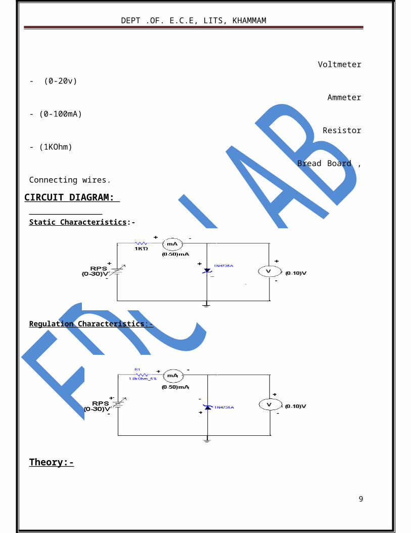
CIRCUIT DIAGRAM: Static Characteristics:-
Regulation Characteristics :-
7
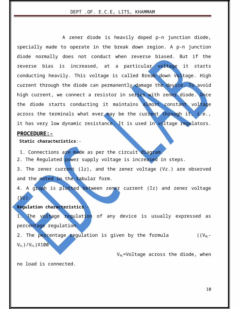
Theory:-
A zener diode is heavily doped p-n junction diode, specially made to operate in the
break down region. A p-n junction diode normally does not conduct when reverse biased. But if the
reverse bias is increased, at a particular voltage it starts conducting heavily. This voltage is called
Break down Voltage. High current through the diode can permanently damage the device. To avoid
high current, we connect a resistor in series with zener diode. Once the diode starts conducting it
maintains almost constant voltage across the terminals what ever may be the current through it, i.e., it
has very low dynamic resistance. It is used in voltage regulators.
PROCEDURE:- Static characteristics:-
1. Connections are made as per the circuit diagram.2. The Regulated power supply voltage is increased in steps.
3. The zener current (lz), and the zener voltage (Vz.) are observed and the noted in the tabular form.
4. A graph is plotted between zener current (Iz) and zener voltage (Vz).
Regulation characteristics:-
1. The voltage regulation of any device is usually expressed as percentage regulation
2. The percentage regulation is given by the formula ((VNL-VFL)/VFL)X100
VNL=Voltage across the diode, when no load is connected.
VFL=Voltage across the diode, when load is connected.
3. Connection are made as per the circuit diagram
4. The load is placed in full load condition and the zener voltage (Vz), Zener current (lz), load current
(IL) are measured.
5. The above step is repeated by decreasing the value of the load in steps.
6. All the readings are tabulated.
7. The percentage regulation is calculated using the above formula
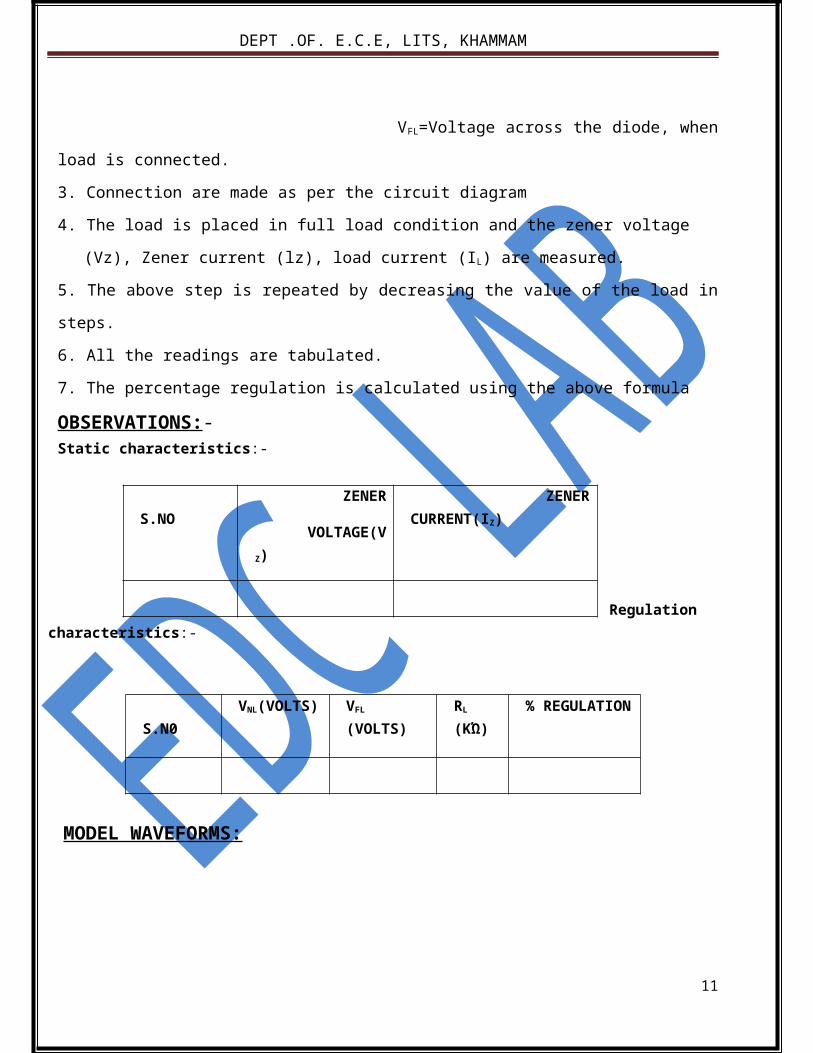
OBSERVATIONS:-Static characteristics:-
8
S.NO ZENER
VOLTAGE(VZ)
ZENER CURRENT(IZ)
Regulation characteristics:-
MODEL WAVEFORMS:
PRECAUTIONS:-
1. The terminals of the zener diode should be properly identified
2. While determined the load regulation, load should not be immediately shorted.
3. Should be ensured that the applied voltages & currents do not exceed the ratings of the diode.
RESULT:-
a) Static characteristics of zener diode are obtained and drawn.
b) Percentage regulation of zener diode is calculated.
VIVA QUESTIONS:-
1. What type of temp? Coefficient does the zener diode have?
2. If the impurity concentration is increased, how the depletion width effected?
3. Does the dynamic impendence of a zener diode vary?
4. Explain briefly about avalanche and zener breakdowns?
5. Draw the zener equivalent circuit and Differentiate between line regulation & load regulation?
9
S.N0
VNL(VOLTS) VFL
(VOLTS)RL
(KΏ)% REGULATION
Exp No : Date :
3. TRANSISTOR COMMON BASE CONFIGURATION
AIM:
1.To observe and draw the input and output characteristics of a transistor connected in common
base configuration.
2. To find α of the given transistor.
APPARATUS:
Transistor - BC 107 Regulated power supply - (0-30V, 1A) Voltmeter - (0-20V) Ammeters - (0-100mA) Resistor - 1KΩ Bread board Connecting wiresTHEORY:
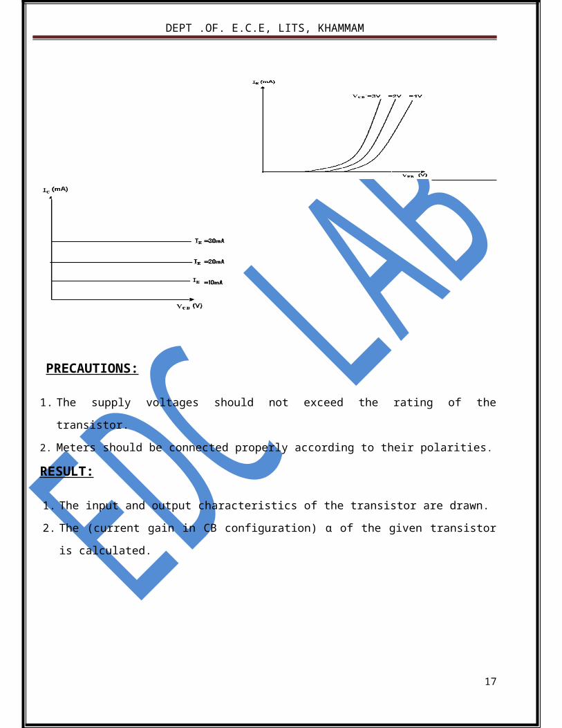
A transistor is a three terminal active device. T he terminals are emitter, base, collector. In CB
configuration, the base is common to both input (emitter) and output (collector). For normal operation,
the E-B junction is forward biased and C-B junction is reverse biased.
In CB configuration, IE is +ve, IC is –ve and IB is –ve. So,
VEB=f1 (VCB,IE) and
IC=f2 (VCB,IB)
With an increasing the reverse collector voltage, the space-charge width at the output junction
increases and the effective base width ‘W’ decreases. This phenomenon is known as “Early effect”.
Then, there will be less chance for recombination within the base region. With increase of charge
gradient within the base region, the current of minority carriers injected across the emitter junction
increases. The current amplification factor of CB configuration is given by,
α= ∆IC/ ∆IE
10
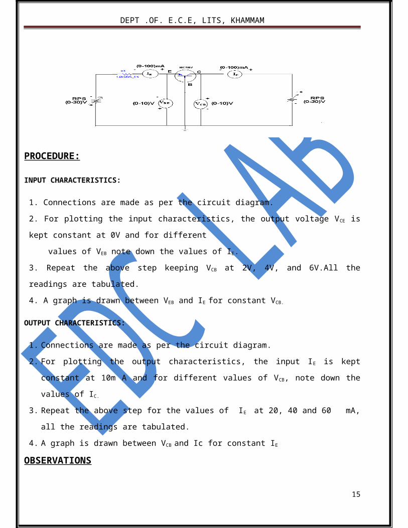
CIRCUIT DIAGRAM
PROCEDURE:
INPUT CHARACTERISTICS:
1. Connections are made as per the circuit diagram.
2. For plotting the input characteristics, the output voltage VCE is kept constant at 0V and for different
values of VEB note down the values of IE.
3. Repeat the above step keeping VCB at 2V, 4V, and 6V.All the readings are tabulated.
4. A graph is drawn between VEB and IE for constant VCB.
OUTPUT CHARACTERISTICS:
1. Connections are made as per the circuit diagram.
2. For plotting the output characteristics, the input IE is kept constant at 10m A and for different
values of VCB, note down the values of IC.
3. Repeat the above step for the values of IE at 20, 40 and 60 mA, all the readings are tabulated.
4. A graph is drawn between VCB and Ic for constant IE
OBSERVATIONS
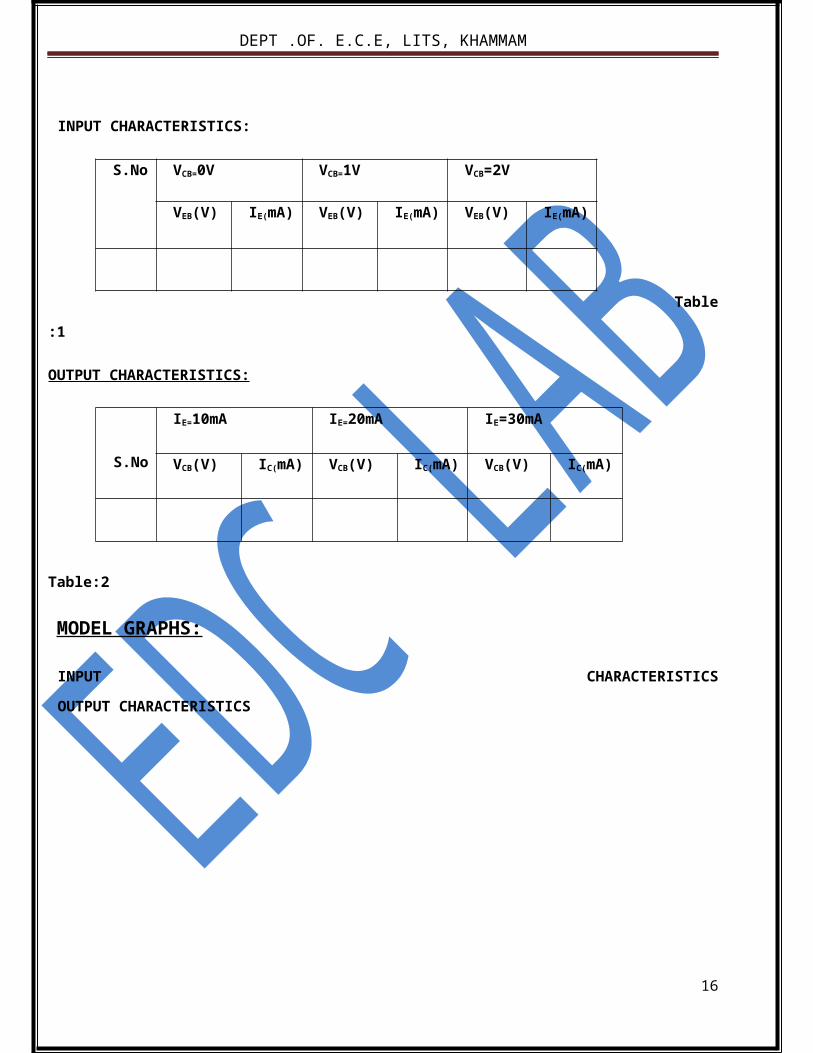
INPUT CHARACTERISTICS:
S.No VCB=0V VCB=1V VCB=2V
VEB(V) IE(mA) VEB(V) IE(mA) VEB(V) IE(mA)
11
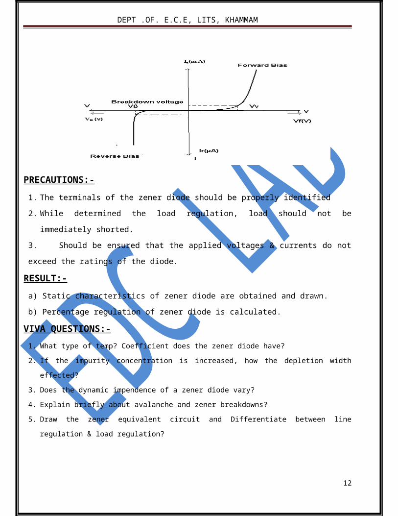
Table:1
OUTPUT CHARACTERISTICS:
S.No
IE=10mA IE=20mA IE=30mA
VCB(V) IC(mA) VCB(V) IC(mA) VCB(V) IC(mA)
Table:2
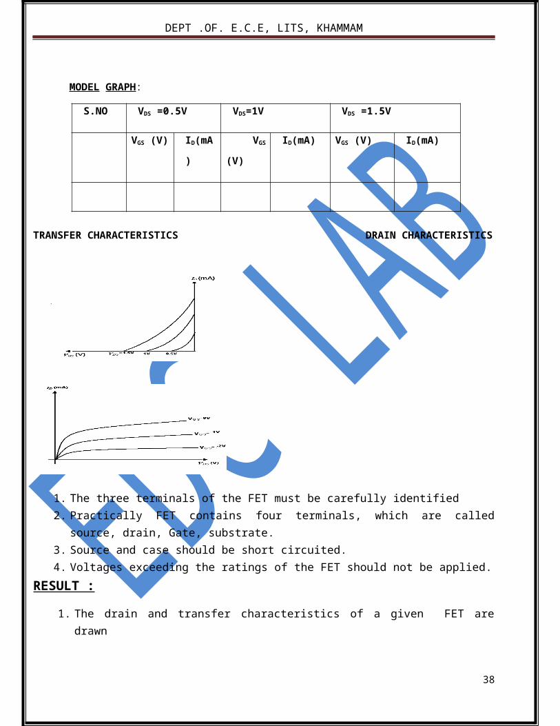
MODEL GRAPHS:
INPUT CHARACTERISTICS OUTPUT CHARACTERISTICS
PRECAUTIONS:
1. The supply voltages should not exceed the rating of the transistor.
2. Meters should be connected properly according to their polarities.
RESULT:
1. The input and output characteristics of the transistor are drawn.
2. The (current gain in CB configuration) α of the given transistor is calculated.
12
VIVA QUESTIONS:
1. What is the range of α for the transistor?
2. Draw the input and output characteristics of the transistor in CB configuration?
3. Identify various regions in output characteristics?
4. What is the relation between α and β?
5. What are the applications of CB configuration?
6. What are the input and output impedances of CB configuration?
7. Define α(alpha)?
8. What is EARLY effect?
9. Draw diagram of CB configuration for PNP transistor?
10. What is the power gain of CB configuration?
13
Exp No: Date:
4. TRANSISTOR CE CHARACTERSTICS
AIM: 1. To draw the input and output characteristics of transistor connected in CE configuration 2. To find β of the given transistor.
APPARATUS:
Transistor - (BC 107) R.P.S - 2Nos (O-30V) Voltmeters - 2Nos (0-20V) Ammeters - (0-200μA) , (0-500mA) Resistors - 1Kohm Bread boardTHEORY:
A transistor is a three terminal device. The terminals are emitter, base, collector. In common
emitter configuration, input voltage is applied between base and emitter terminals and out put is taken
across the collector and emitter terminals. Therefore the emitter terminal is common to both input and
output. The input characteristics resemble that of a forward biased diode curve. This is expected since
the Base-Emitter junction of the transistor is forward biased. As compared to CB arrangement IB
increases less rapidly with VBE . Therefore input resistance of CE circuit is higher than that of CB
circuit.
The output characteristics are drawn between I c and VCE at constant IB. the collector current
varies with VCE unto few volts only. After this the collector current becomes almost constant, and
independent of VCE. The value of VCE up to which the collector current changes with V CE is known as
Knee voltage. The transistor always operated in the region above Knee voltage, IC is always constant
and is approximately equal to IB.
The current amplification factor of CE configuration is given by
Β = ΔIC/ΔIB
14
CIRCUIT DIAGRAM:
PROCEDURE:
INPUT CHARECTERSTICS:
1. Connect the circuit as per the circuit diagram.
2. For plotting the input characteristics the output voltage VCE is kept constant at 1V and for
different values of VBE . Note down the values of IC
3. Repeat the above step by keeping VCE at 2V and 4V.
4. Tabulate all the readings.
5. plot the graph between VBE and IB for constant VCE
OUTPUT CHARACTERSTICS:
1. Connect the circuit as per the circuit diagram
2. for plotting the output characteristics the input current IB is kept constant at 10μA and for
different values of VCE note down the values of IC
3. repeat the above step by keeping IB at 75 μA 100 μA
4. Tabulate the all the readings
5. Plot the graph between VCE and IC for constant IB
15
OBSERVATIONS:
INPUT CHARACTERISTICS:
S.NOVCE = 1V VCE = 2V VCE = 4V
VBE(V) IB(μA) VBE(V) IB(μA) VBE(V) IB(μA)
Table:1
OUTPUT CHAREACTARISTICS:
S.NOIB = 50 μA IB = 75 μA IB = 100 μA
VCE(V) IC(mA) VCE(V) ICmA) VCE(V) IC(mA)
Table:2
16
MODEL GRAPHS:
INPUT CHARACTERSTICS: OUTPUT CHARECTERSTICS:
PRECAUTIONS:
1. The supply voltage should not exceed the rating of the transistor
2. Meters should be connected properly according to their polarities
RESULT:
1. The input and output characteristics of a transistor in CE configuration are Drawn
2. The β of a given transistor is calculated
VIVA QUESTIONS:
1. What is the range of β for the transistor?
2. What are the input and output impedances of CE configuration?
3. Identify various regions in the output characteristics?
4. what is the relation between α and β
5. Define current gain in CE configuration?
6. Why CE configuration is preferred for amplification?
7. What is the phase relation between input and output?
8. Draw diagram of CE configuration for PNP transistor?
17
9. What is the power gain, application of CE configuration?
Exp No Date:
5. HALFWAVE RECTIFIER
AIM
To find the ripple factor, % Regulation and efficiency of a half-wave rectifier by using Filter and
without Filter.
APPARATUS
Multimeters - 1No’s.
Transformer - (9-0-9) V.
Diode - 1N 4007
Capacitor - 100μf.
Resistor - 1KΩ.
Connecting wires
THEORY
During positive half-cycle of the input voltage, the diode D1 is in forward bias and conducts
through the load resistor R1. Hence the current produces an output voltage across the load resistor R1,
which has the same shape as the +ve half cycle of the input voltage.
During the negative half-cycle of the input voltage, the diode is reverse biased and there is no
current through the circuit. i.e, the voltage across R1 is zero. The net result is that only the +ve half
cycle of the input voltage appears across the load. The average value of the half wave rectified o/p
voltage is the value measured on dc voltmeter.
For practical circuits, transformer coupling is usually provided for two reasons.
1. The voltage can be stepped-up or stepped-down, as needed.
2. The ac source is electrically isolated from the rectifier. Thus preventing shock hazards in the
secondary circuit.
18
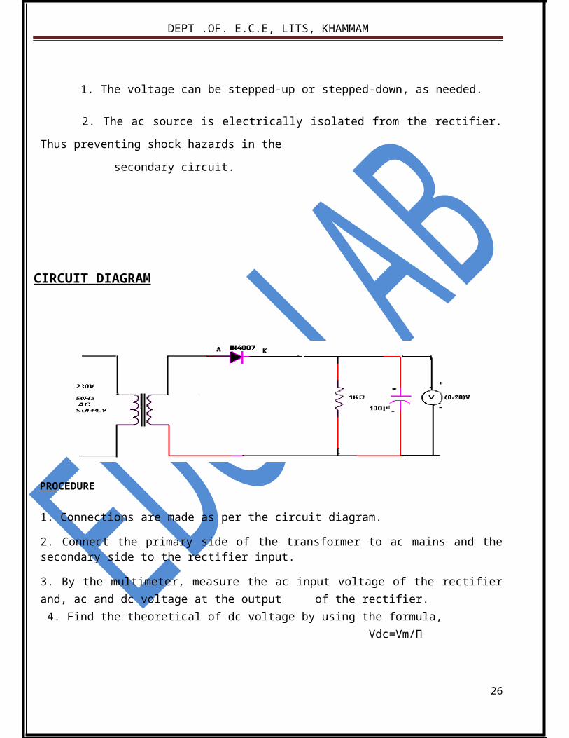
CIRCUIT DIAGRAM
PROCEDURE
1. Connections are made as per the circuit diagram.
2. Connect the primary side of the transformer to ac mains and the secondary side to the rectifier input.
3. By the multimeter, measure the ac input voltage of the rectifier and, ac and dc voltage at the output of the rectifier. 4. Find the theoretical of dc voltage by using the formula,
Vdc=Vm/П
Where, Vm=2Vrms, (Vrms=output ac voltage.)
The Ripple factor is calculated by using the formula
r =ac output voltage/dc output voltage.
REGULATION CHARACTERSTICS
1. Connections are made as per the circuit diagram.
2. By increasing the value of the rheostat, the voltage across the load and current flowing
through the load are measured.
3. The reading is tabulated.
4. Draw a graph between load voltage (VL and load current ( IL ) taking VL on X-axis and IL on
y-axis
19
5. From the value of no-load voltages, the %regulation is calculated using the formula
Theoretical calculations for Ripple factor
Without Filter :-
Vrms=Vm/2
Vm=2Vrms
Vdc=Vm/П
Ripple factor r=√ (Vrms/ Vdc )2 -1 =1.21
With Filter:-
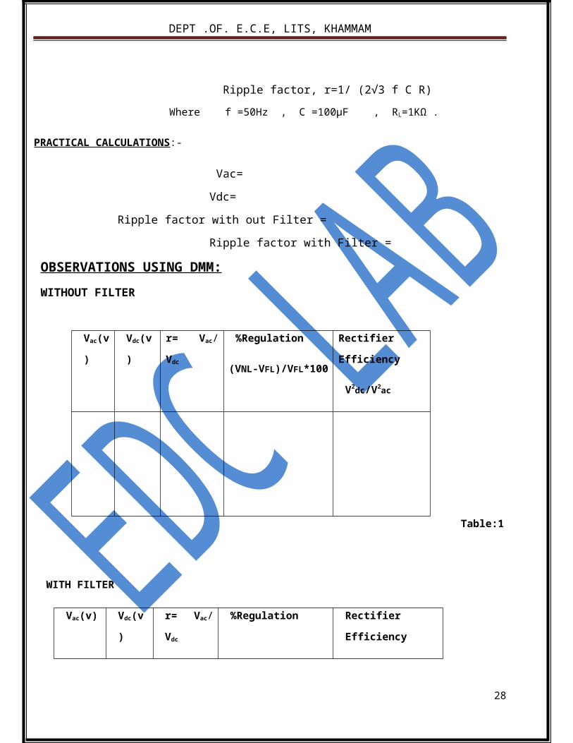
Ripple factor, r=1/ (2√3 f C R)
Where f =50Hz , C =100µF , RL=1KΩ .
PRACTICAL CALCULATIONS:-
Vac=
Vdc=
Ripple factor with out Filter =
Ripple factor with Filter =
OBSERVATIONS USING DMM:
WITHOUT FILTER
Vac(v) Vdc(v) r= Vac/ Vdc %Regulation
(VNL-VFL)/VFL*100
Rectifier Efficiency
V2dc/V2ac
Table:1
20
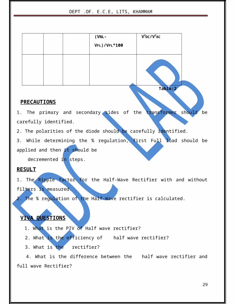
WITH FILTER
Vac(v) Vdc(v) r= Vac/ Vdc %Regulation
(VNL-VFL)/VFL*100
Rectifier Efficiency
V2DC/V2AC
Table:2
PRECAUTIONS
1. The primary and secondary sides of the transformer should be carefully identified.
2. The polarities of the diode should be carefully identified.
3. While determining the % regulation, first Full load should be applied and then it should be
decremented in steps.
RESULT
1. The Ripple factor for the Half-Wave Rectifier with and without filters is measured.
2. The % regulation of the Half-Wave rectifier is calculated.
VIVA QUESTIONS
1. What is the PIV of Half wave rectifier?
2. What is the efficiency of half wave rectifier?
3. What is the rectifier?
4. What is the difference between the half wave rectifier and full wave Rectifier?
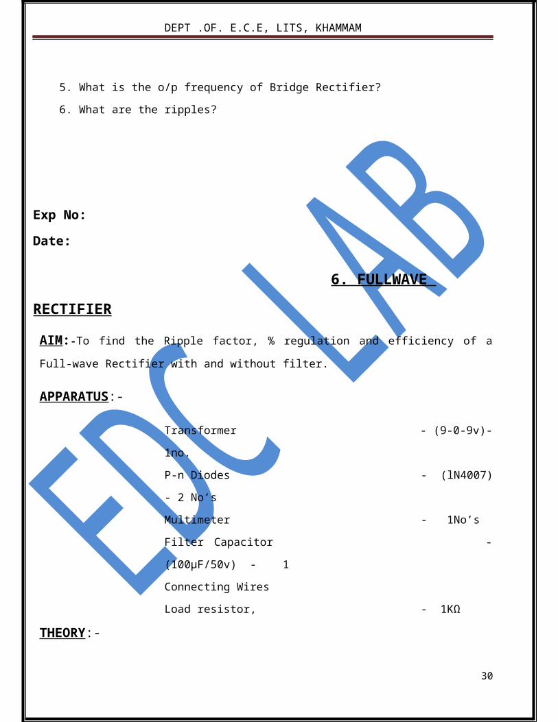
5. What is the o/p frequency of Bridge Rectifier?
6. What are the ripples?
21
Exp No: Date:
6. FULLWAVE RECTIFIER
AIM:-To find the Ripple factor, % regulation and efficiency of a Full-wave Rectifier with and
without filter.
APPARATUS:-
Transformer - (9-0-9v)- 1no.
P-n Diodes - (lN4007) - 2 No’s
Multimeter - 1No’s
Filter Capacitor - (100μF/50v) - 1
Connecting Wires
Load resistor, - 1KΩ
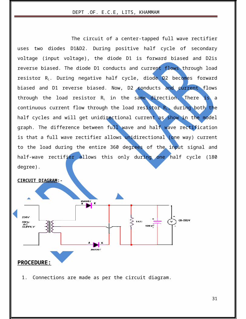
THEORY:- The circuit of a center-tapped full wave rectifier uses two diodes D1&D2. During
positive half cycle of secondary voltage (input voltage), the diode D1 is forward biased and D2is
reverse biased. The diode D1 conducts and current flows through load resistor RL. During negative half
cycle, diode D2 becomes forward biased and D1 reverse biased. Now, D2 conducts and current flows
through the load resistor RL in the same direction. There is a continuous current flow through the load
resistor RL, during both the half cycles and will get unidirectional current as show in the model graph.
The difference between full wave and half wave rectification is that a full wave rectifier allows
unidirectional (one way) current to the load during the entire 360 degrees of the input signal and half-
wave rectifier allows this only during one half cycle (180 degree).
CIRCUIT DIAGRAM:-
22
PROCEDURE:
1. Connections are made as per the circuit diagram.
3. Connect the ac mains to the primary side of the transformer and the secondary side to the
rectifier.
4. Measure the ac voltage at the input side of the rectifier.
5. Measure both ac and dc voltages at the output side the rectifier.
6. Find the theoretical value of the dc voltage by using the formula Vdc=2Vm/П
7. Connect the filter capacitor across the load resistor and measure the values of Vac and Vdc at the
output.
8. The theoretical values of Ripple factors with and without capacitor are calculated.
9. From the values of Vac and Vdc practical values of Ripple factors are calculated. The practical values
are compared with theoretical values.
THEORITICAL CALCULATIONS:-
Vrms = Vm/ √2 Vm =Vrms√2 Vdc=2Vm/П (i)Without filter: Ripple factor, r = √ ( Vrms/ Vdc )2 -1 = 0.482(ii)With filter: Ripple factor, r = 1/ (4√3 f C RL) where f =50Hz C =100µF RL=1KΩ
PRACTICAL CALCULATIONS USING DMM:
Without Filter:
Load Resistor Vac(v) Vdc(v) r= Vac/ Vdc %Regulation
(VNL-VFL)/VFL*100
Rectifier Efficiency
V2DC/V2AC
Table:1
23
With Filter
Load Resistor Vac(v) Vdc(v) r= Vac/ Vdc %Regulation
(VNL-VFL)/VFL*100
Rectifier Efficiency
V2dc/V2ac
Table:2
PRECAUTIONS:
1. The primary and secondary side of the transformer should be carefully identified
2. The polarities of all the diodes should be carefully identified.
RESULT:-
The ripple factor of the Full-wave rectifier (with filter and without filter) is calculated.
VIVA QUESTIONS:-
1. Define regulation of the full wave rectifier?
2. Define peak inverse voltage (PIV)? And write its value for Full-wave rectifier?
3. If one of the diode is changed in its polarities what wave form would you get?
4. Does the process of rectification alter the frequency of the waveform?
5. What is ripple factor of the Full-wave rectifier?
6. What is the necessity of the transformer in the rectifier circuit?
7. What are the applications of a rectifier?
8. What is meant by ripple and define Ripple factor?
9. Explain how capacitor helps to improve the ripple factor?
10. Can a rectifier made in INDIA (V=230v, f=50Hz) be used in USA (V=110v, f=60Hz)?
24
Exp No: Date :
7. FET CHARACTERISTICS
AIM : a). To draw the drain and transfer characteristics of a given FET. b). To find the drain resistance (rd) amplification factor (μ) and Transconductance (gm) of
the given FET.
APPARATUS:
FET - (BFW-11)
Regulated power supply
Voltmeter - (0-20V)
Ammeter - (0-100mA)
Bread board
Connecting wires
THEORY:
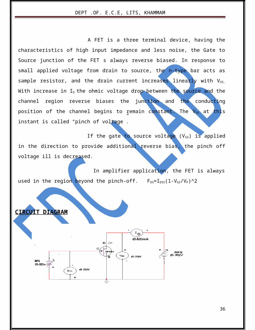
A FET is a three terminal device, having the characteristics of high input impedance and
less noise, the Gate to Source junction of the FET s always reverse biased. In response to small applied
voltage from drain to source, the n-type bar acts as sample resistor, and the drain current increases
linearly with VDS. With increase in ID the ohmic voltage drop between the source and the channel region
reverse biases the junction and the conducting position of the channel begins to remain constant. The
VDS at this instant is called “pinch of voltage”.
If the gate to source voltage (VGS) is applied in the direction to provide additional reverse
bias, the pinch off voltage ill is decreased.
In amplifier application, the FET is always used in the region beyond the pinch-off.
FDS=IDSS(1-VGS/VP)^2
25
CIRCUIT DIAGRAM
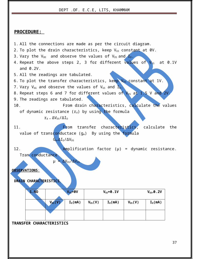
PROCEDURE:
1. All the connections are made as per the circuit diagram.2. To plot the drain characteristics, keep VGS constant at 0V.3. Vary the VDD and observe the values of VDS and ID.4. Repeat the above steps 2, 3 for different values of VGS at 0.1V and 0.2V.5. All the readings are tabulated.6. To plot the transfer characteristics, keep VDS constant at 1V.7. Vary VGG and observe the values of VGS and ID.8. Repeat steps 6 and 7 for different values of VDS at 1.5 V and 2V.9. The readings are tabulated.10. From drain characteristics, calculate the values of dynamic resistance (rd) by using the formula
rd = ∆VDS/∆ID
11. From transfer characteristics, calculate the value of transconductace (gm) By using the formulaGm=∆ID/∆VDS
12. Amplification factor (μ) = dynamic resistance. Tran conductanceμ = ∆VDS/∆VGS
OBSERVATIONS :
DRAIN CHARACTERISTICS:
S.NO VGS=0V VGS=0.1V VGS=0.2V
VDS(V) ID(mA) VDS(V) ID(mA) VDS(V) ID(mA)
26
TRANSFER CHARACTERISTICS
MODEL GRAPH:
TRANSFER CHARACTERISTICS DRAIN CHARACTERISTICS
PRECAUTIONS: 1. The three terminals of the FET must be carefully identified2. Practically FET contains four terminals, which are called source, drain, Gate, substrate.3. Source and case should be short circuited.4. Voltages exceeding the ratings of the FET should not be applied.
RESULT :
1. The drain and transfer characteristics of a given FET are drawn2. The dynamic resistance (rd), amplification factor (μ) and Tran conductance (gm) of the given
FET are calculated.
VIVA QUESTIONS:
1. What are the advantages and applications of FET?
2. Different between FET and BJT. Draw the different types..
27
S.NO VDS =0.5V VDS=1V VDS =1.5V
VGS (V) ID(mA) VGS (V) ID(mA) VGS (V) ID(mA)
3. Explain different regions of V-I characteristics of FET?
4. What are the types of FET?
5. What are the parameters and disadvantages of FET?
Exp No: Date :
8. h-PARAMETERS OF CE CONFIGURATION
AIM: To calculate the H-parameters of transistor in CE configuration.
APPRATUS:
Transistor - BC 107
Resistors - 100 K Ώ , 100 Ώ
Ammeters - (0-200µA), (0-200mA)
Voltmeters - (0-20V) - 2Nos
Regulated Power Supply - (0-30V, 1A) - 2Nos
Breadboard
THEORY:
INPUT CHARACTERISTICS:
The two sets of characteristics are necessary to describe the behavior of the CE configuration one for input or base emitter circuit and other for the output or collector emitter circuit.
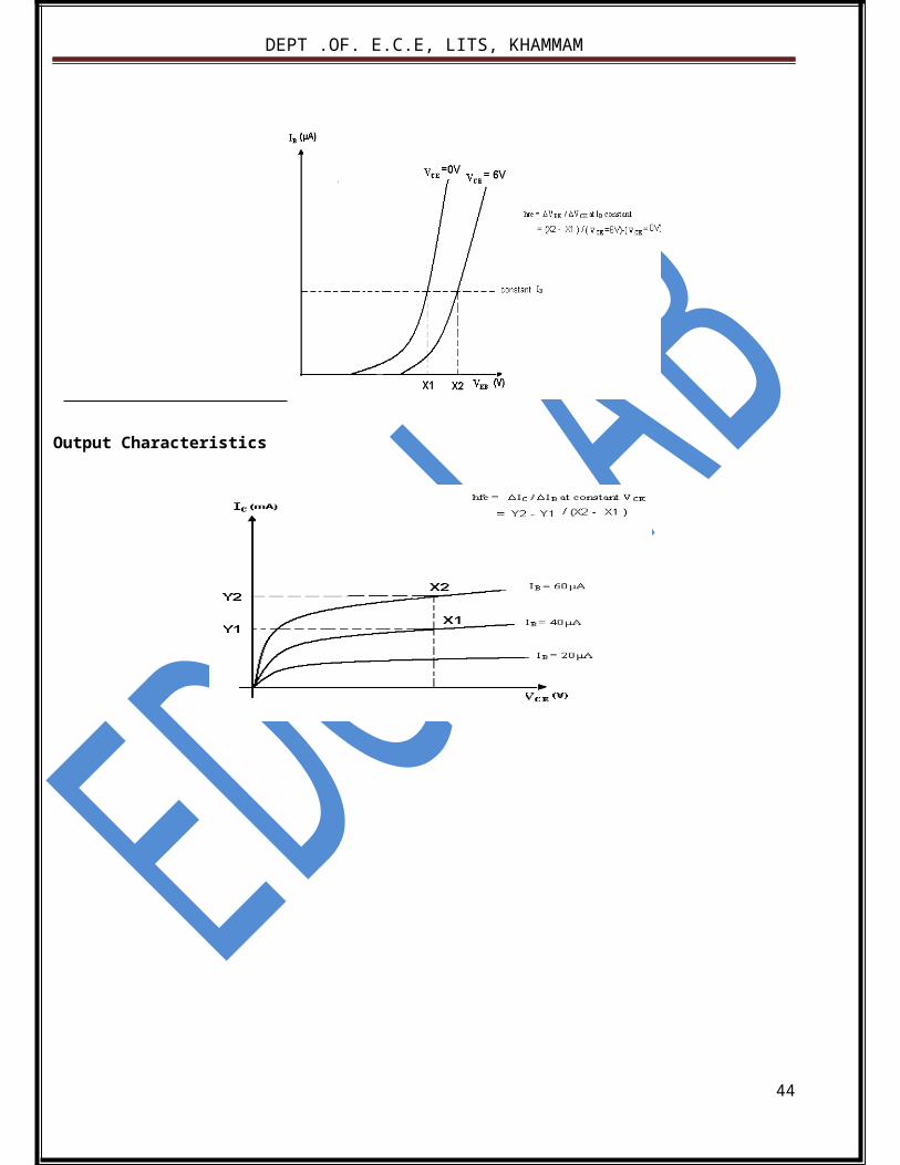
In input characteristics the emitter base junction forward biased by a very small voltage VBB where as collector base junction reverse biased by a very large voltage VCC. The input characteristics are a plot of input current IB Vs the input voltage VBE for a range of values of output voltage VCE . The following important points can be observed from these characteristics curves.
1. The characteristics resemble that of CE configuration.2. Input resistance is high as IB increases less rapidly with VBE
3. The input resistance of the transistor is the ratio of change in base emitter voltage ΔVBE to change in base current ΔIB at constant collector emitter voltage ( VCE) i.e... Input resistance or input impedance hie = ΔVBE / ΔIB at VCE constant.
OUTPUT CHARACTERISTICS:
28
A set of output characteristics or collector characteristics are a plot of out put current I C
VS output voltage VCE for a range of values of input current IB .The following important points can be
observed from these characteristics curves:-
1. The transistor always operates in the active region. I.e. the collector current
IC increases with VCE very slowly. For low values of the VCE the IC increases rapidly with a small
increase in VCE .The transistor is said to be working in saturation region.
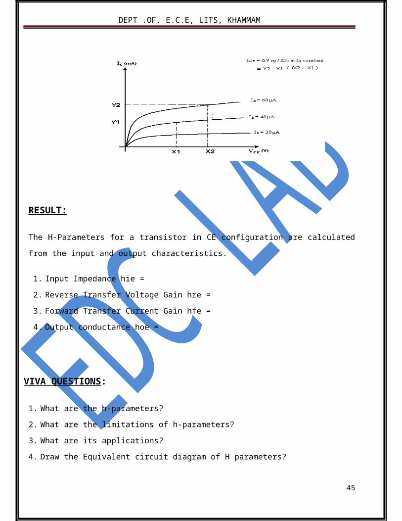
Output resistance is the ratio of change of collector emitter voltage ΔVCE , to change in collector
current ΔIC with constant IB. Output resistance or Output impedance hoe = ΔVCE / ΔIC at IB constant.
Input Impedance hie = ΔVBE / ΔIB at VCE constant
Output impedance hoe = ΔVCE / ΔIC at IB constant
Reverse Transfer Voltage Gain hre = ΔVBE / ΔVCE at IB constant
Forward Transfer Current Gain hfe = ΔIC / ΔIB at constant VCE
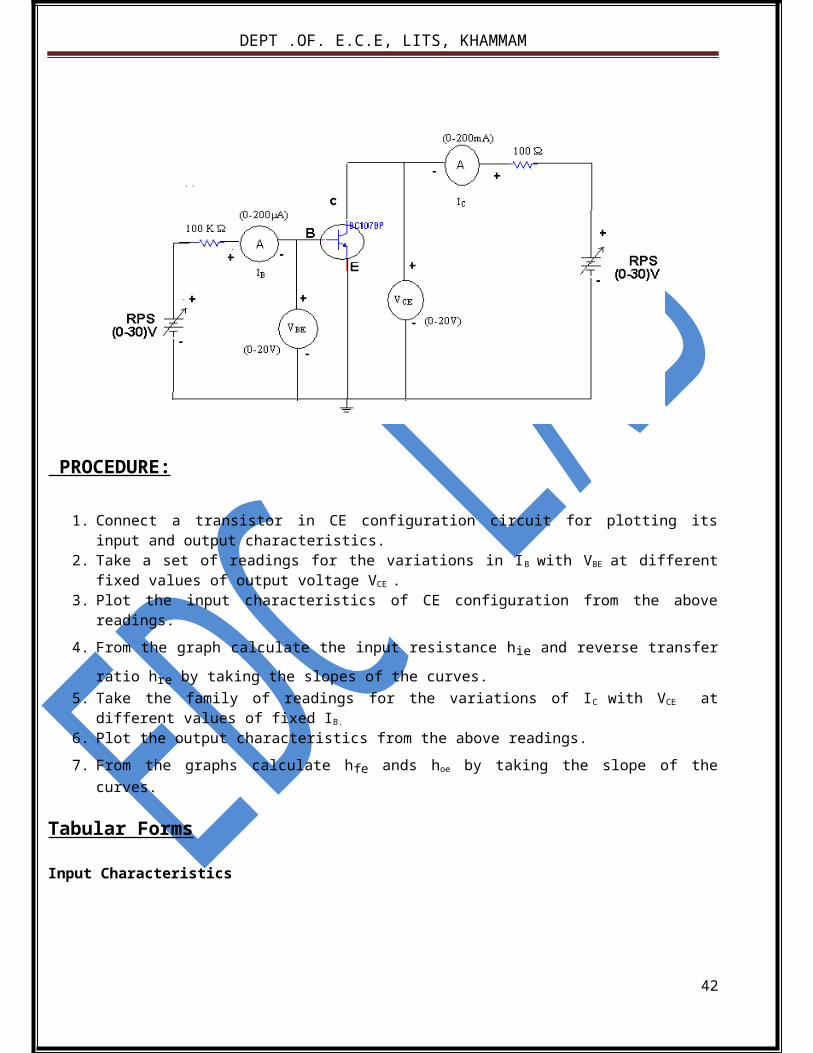
CIRCUIT DIAGRAM:
PROCEDURE:
1. Connect a transistor in CE configuration circuit for plotting its input and output characteristics.2. Take a set of readings for the variations in IB with VBE at different fixed values of output voltage VCE .3. Plot the input characteristics of CE configuration from the above readings.
29
4. From the graph calculate the input resistance hie and reverse transfer ratio hre by taking the slopes of the curves.
5. Take the family of readings for the variations of IC with VCE at different values of fixed IB.
6. Plot the output characteristics from the above readings.
7. From the graphs calculate hfe ands hoe by taking the slope of the curves.
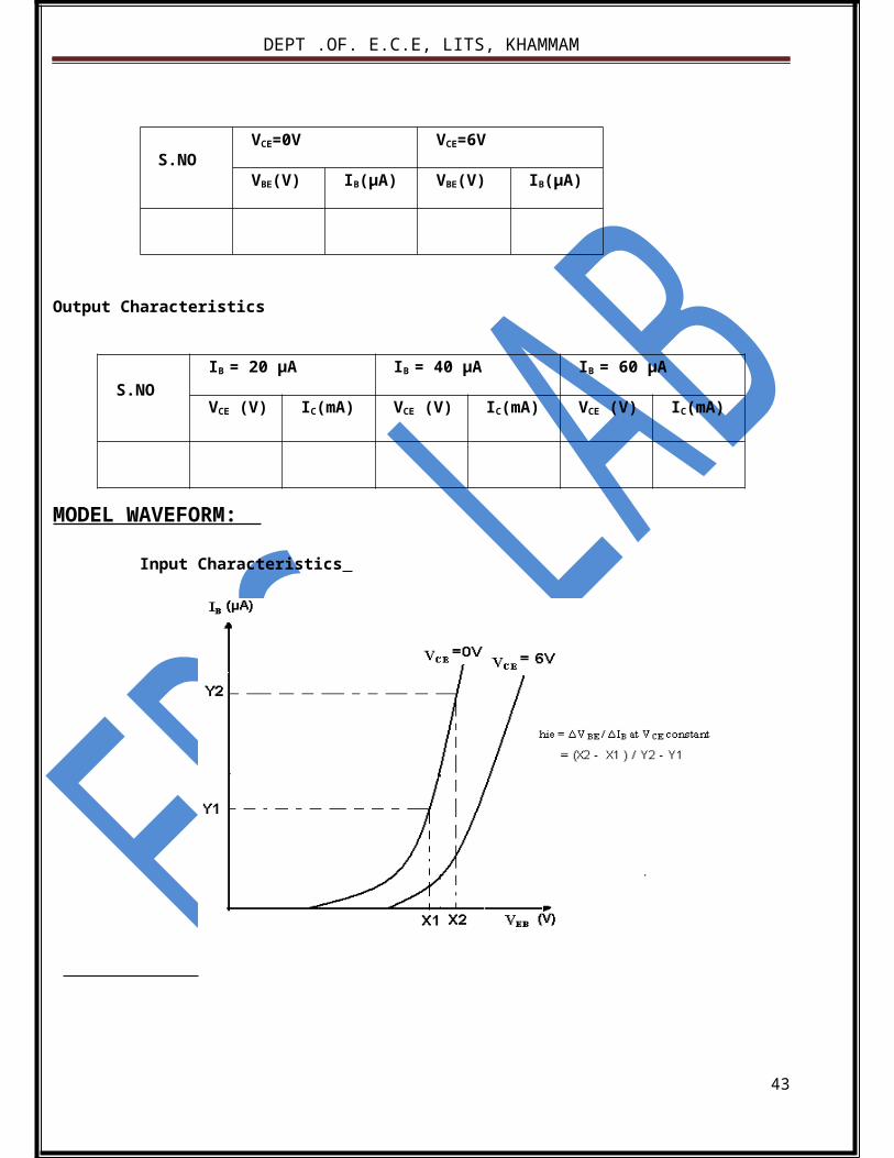
Tabular Forms
Input Characteristics
S.NOVCE=0V VCE=6V
VBE(V) IB(μA) VBE(V) IB(μA)
Output Characteristics
MODEL WAVEFORM:
Input Characteristics
30
S.NOIB = 20 µA IB = 40 µA IB = 60 µA
VCE (V) IC(mA) VCE (V) IC(mA) VCE (V) IC(mA)
Output Characteristics
31
RESULT:
The H-Parameters for a transistor in CE configuration are calculated from the input and output
characteristics.
1. Input Impedance hie =
2. Reverse Transfer Voltage Gain hre =
3. Forward Transfer Current Gain hfe =
4. Output conductance hoe =
32

VIVA QUESTIONS:
1. What are the h-parameters?
2. What are the limitations of h-parameters?
3. What are its applications?
4. Draw the Equivalent circuit diagram of H parameters?
5. Define H parameter?
6. What are tabular forms of H parameters monoculture of a transistor?
7. What is the general formula for input impedance?
8. What is the general formula for Current Gain?
9. What is the general formula for Voltage gain?
33

Exp No: Date:
9.TRANSISTOR CE AMPLIFIER
AIM: 1. To Measure the voltage gain of a CE amplifier
2. To draw the frequency response curve of the CE amplifier
APPARATUS: Transistor - BC-107
Regulated power Supply - (0-30V, 1A)
Resistors - [33KΩ, 3.3KΩ, 330Ω, 1.5KΩ
1KΩ, 2.2KΩ, 4.7KΩ]
Capacitors - 10µF -2No , 100µF-1 no.
Function Generator
CRO
Bread Board, Connecting Wires
THEORY:
The CE amplifier provides high gain &wide frequency response. The emitter lead is
common to both input & output circuits and is grounded. The emitter-base circuit is forward biased.
The collector current is controlled by the base current rather than emitter current. The input signal is
applied to base terminal of the transistor and amplifier output is taken across collector terminal. A very
small change in base current produces a much larger change in collector current. When +VE half-cycle
is fed to the input circuit, it opposes the forward bias of the circuit which causes the collector current to
decrease, it decreases the voltage more –VE. Thus when input cycle varies through a -VE half-cycle,
increases the forward bias of the circuit, which causes the collector current to increases thus the output
signal is common emitter amplifier is in out of phase with the input signal.
34
CIRCUIT DIAGRAM:
PROCEDURE:
1. Connect the circuit as shown in circuit diagram
2. Apply the input of 20mV peak-to-peak and 1 KHz frequency using Function Generator
3. Measure the Output Voltage Vo (p-p) for various load resistors
4. Tabulate the readings in the tabular form.
5. The voltage gain can be calculated by using the expression Av= (V0/Vi)
6. For plotting the frequency response the input voltage is kept Constant at 20mV peak-to-peak and
the frequency is varied from 100Hz to 1MHz Using function generator
7. Note down the value of output voltage for each frequency.
8. All the readings are tabulated and voltage gain in dB is calculated by Using
the expression Av=20 log10 (V0/Vi)
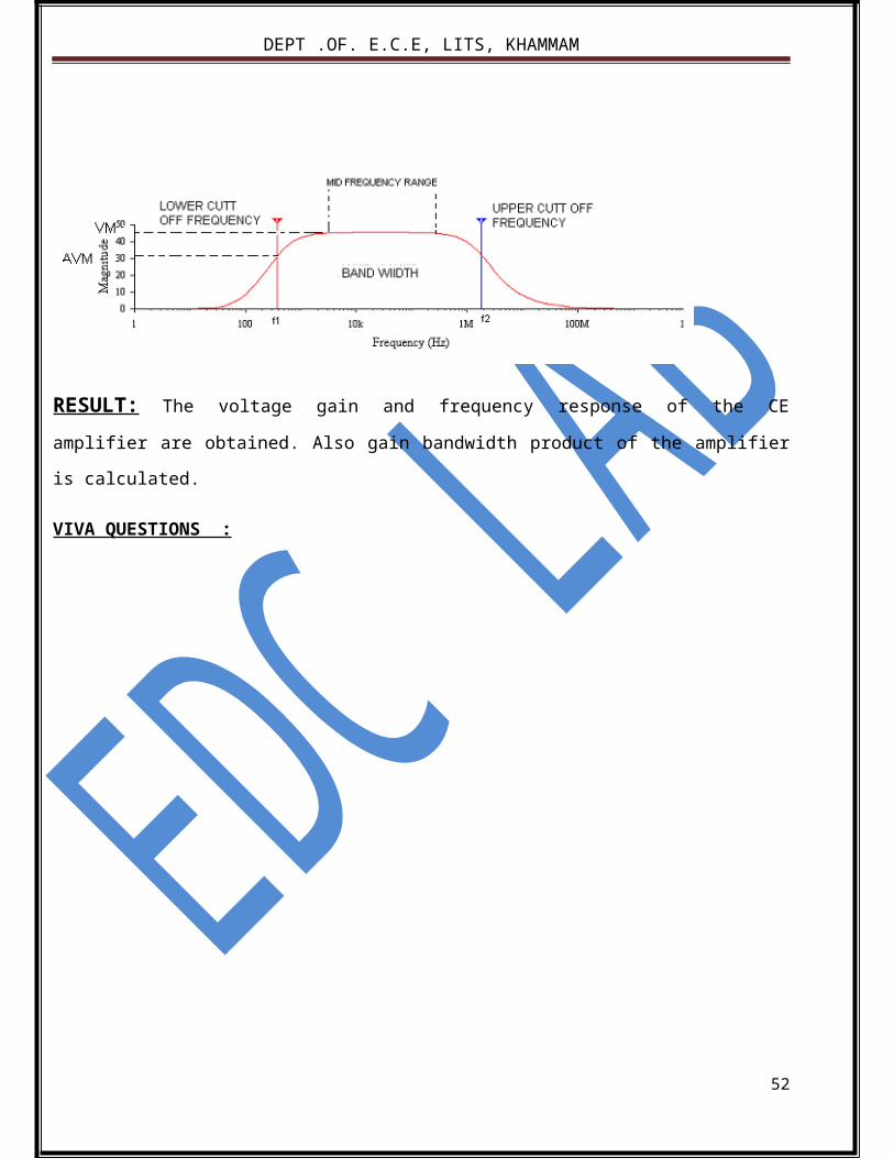
9. A graph is drawn by taking frequency on x-axis and gain in dB on y-axis on Semi-log graph.
The band width of the amplifier is calculated from the graph using the expression,
Bandwidth, BW=f2-f1
Where f1 lower cut-off frequency of CE amplifier, and
Where f2 upper cut-off frequency of CE amplifier
The bandwidth product of the amplifier is calculated using the Expression
Gain Bandwidth product=3-dBmidband gain X Bandwidth
35
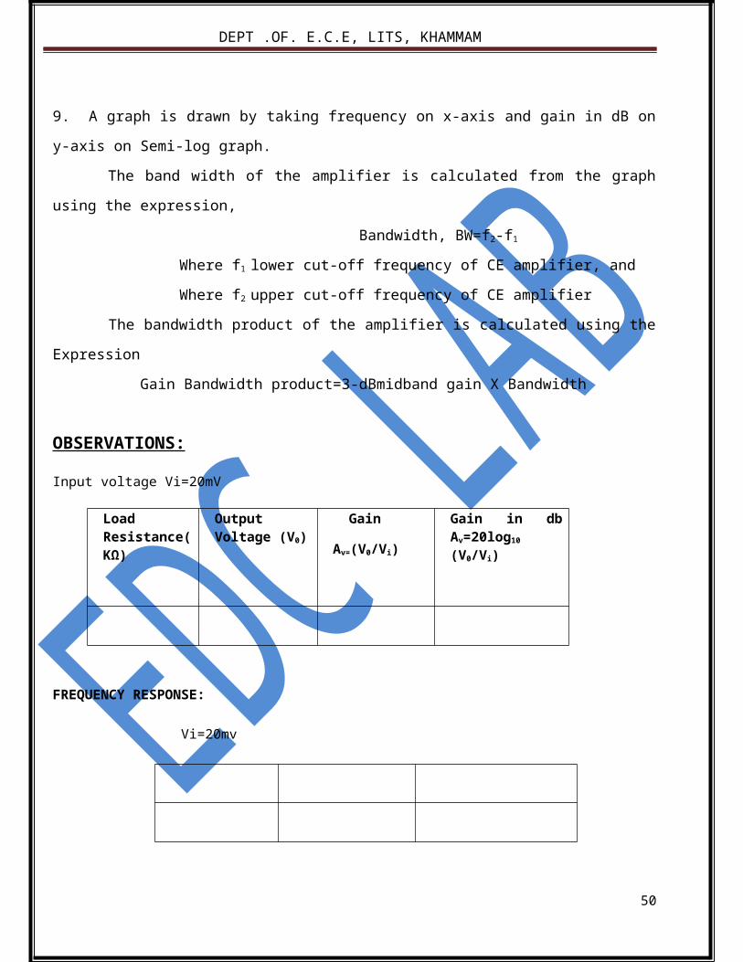
OBSERVATIONS:
Input voltage Vi=20mV
Load Resistance(KΩ)
Output Voltage (V0)
Gain
Av=(V0/Vi)
Gain in db Av=20log10 (V0/Vi)
FREQUENCY RESPONSE:
Vi=20mv
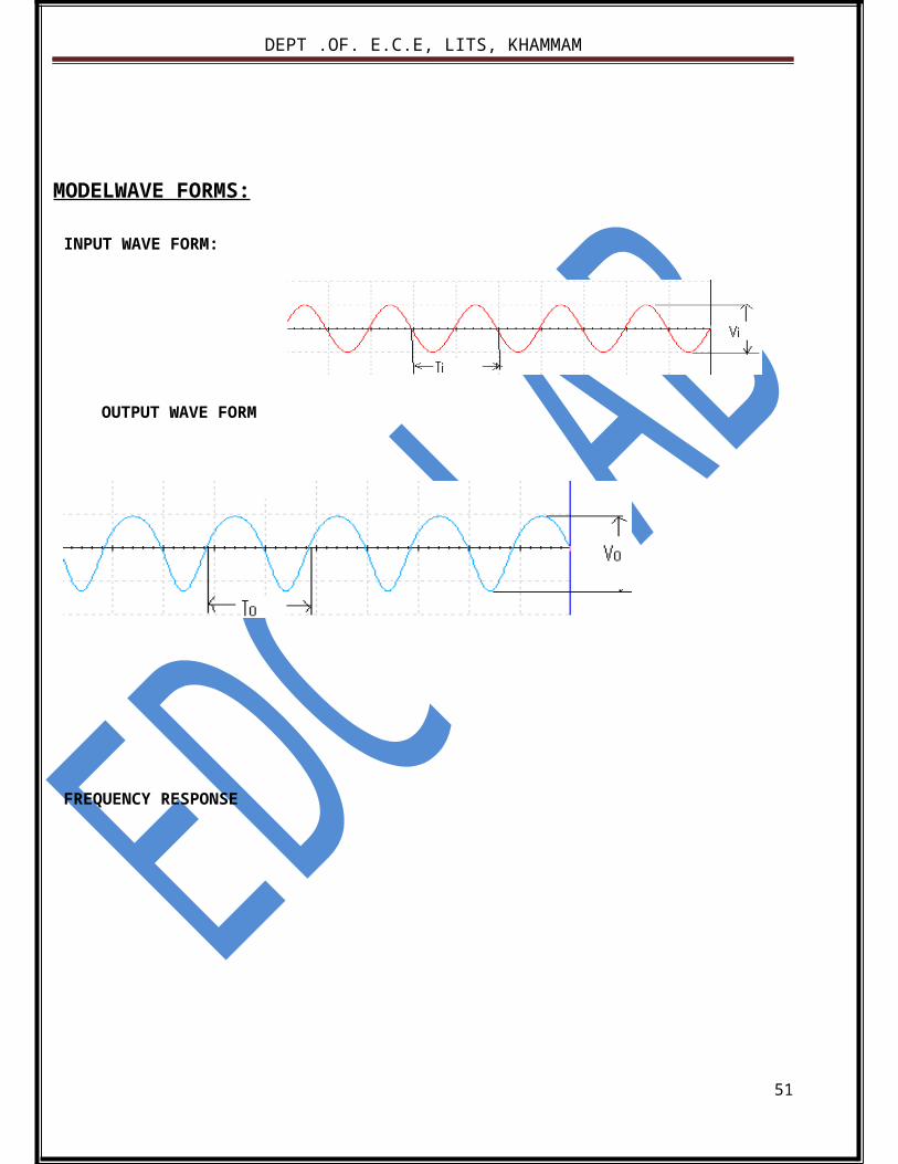
MODELWAVE FORMS:
INPUT WAVE FORM:
OUTPUT WAVE FORM
36
FREQUENCY RESPONSE
RESULT: The voltage gain and frequency response of the CE amplifier are obtained. Also gain
bandwidth product of the amplifier is calculated.
VIVA QUESTIONS :
37
38
Exp No: Date :
10. COMMON COLLECTOR AMPLIFIER
AIM: 1. To measure the voltage gain of a CC amplifier
2. To draw the frequency response of the CC amplifier
APPARATUS:
CRO
Transistor - BC-107
Resistors - [33KΩ, 3.3KΩ, 330Ω, 1.5KΩ 1KΩ, 2.2KΩ, 4.7KΩ] Capacitors - 10µF -2No , 100µF-1 no. Regulated power Supply - (0-30V, 1A) Function Generator Bread Board, Connecting Wires
THEORY:
In common-collector amplifier the input is given at the base and the output is taken at the
emitter. In this amplifier, there is no phase inversion between input and output. The input impedance of
the CC amplifier is very high and output impedance is low.
The voltage gain is less than unity. Here the collector is at ac ground and the capacitors used
must have a negligible reactance at the frequency of operation.
This amplifier is used for impedance matching and as a buffer amplifier. This circuit is also
known as emitter follower.
39
CIRCUIT DIAGRAM:
PROCEDURE:
1. Connections are made as per the circuit diagram.2. For calculating the voltage gain the input voltage of 20mV peak-to-peak and 1 KHz frequency is
applied and output voltage is taken for various load resistors.3. The readings are tabulated.
The voltage gain calculated by using the expression, Av=V0/Vi
4. For plotting the frequency response the input voltage is kept constant a 20mV peak-to- peak and the frequency is varied from 100Hzto 1MHz.5. Note down the values of output voltage for each frequency.
All the readings are tabulated the voltage gain in dB is calculated by using
the expression, Av=20log 10(V0/Vi)
6. A graph is drawn by taking frequency on X-axis and gain in dB on y-axis on Semi-log graph sheet. The Bandwidth of the amplifier is calculated from the graph using
the Expression, Bandwidth BW=f2-f1
Where f1 is lower cut-off frequency of CE amplifier
f2 is upper cut-off frequency of CE amplifier
10. The gain Bandwidth product of the amplifier is calculated using the Expression,
Gain -Bandwidth product=3-dB midband gain X Bandwidth
40
OBSERVATIONS:
Load Resistance(KΩ) Output Voltage( V0) Gain
Av=V0/Vi
Gain In Db
Av=20log 10(V0/Vi)
Table:1
FREQUENCY RESPONSE: Vi=20mV
FREQUENCY(Hz) OUTPUT
VOLTAGE( V0)
GAIN IN dB
Av=20log 10(V0/Vi)
Table:2
WAVEFORM:
INPUT WAVEFORM
41
OUTPUT WAVEFORM
PRECAUTIONS
1. The input voltage must be kept constant while taking frequency response.
2. Proper biasing voltages should be applied.
RESULT:
The voltage gain and frequency response of the CC amplifier are obtained. Also gain
Bandwidth product is calculated.
VIVA QUESTIONS:
1. What are the applications of CC amplifier?
2. What is the voltage gain of CC amplifier?
3. What are the values of input and output impedances of the CC amplifier?
4. To which ground the collector terminal is connected in the circuit?
5. Identify the type of biasing used in the circuit?
6. Give the relation between α, β and γ.
7. Write the other name of CC amplifier?
8. What are the differences between CE,CB and CC?
9. When compared to CE, CC is not used for amplification. Justify your answer?
10. What is the phase relationship between input and output in CC?
42
Exp No: Date :
11.COMMON SOURCE FET AMPLIFIER
AIM : 1. To obtain the frequency response of the common source FET Amplifier
2. To find the Bandwidth.
APPRATUS :
N-channel FET (BFW11)
Resistors (6.8KΩ, 1MΩ, 1.5KΩ)
Capacitors (0.1µF, 47µF)
Regulated power Supply (0-30V)
Function generator
CRO
CRO probes
Bread board
Connecting wires
CIRCUIT DIAGRAM:
43
THEORY:
A field-effect transistor (FET) is a type of transistor commonly used for weak-signal
amplification (for example, for amplifying wireless (signals). The device can amplify analog or digital
signals. It can also switch DC or function as an oscillator. In the FET, current flows along a
semiconductor path called the channel. At one end of the channel, there is an electrode called the
source. At the other end of the channel, there is an electrode called the drain. The physical diameter of
the channel is fixed, but its effective electrical diameter can be varied by the application of a voltage to
a control electrode called the gate. Field-effect transistors exist in two major classifications. These are
known as the junction FET (JFET) and the metal-oxide- semiconductor FET (MOSFET). The junction
FET has a channel consisting of N-type semiconductor (N-channel) or P-type semiconductor (P-
channel) material; the gate is made of the opposite semiconductor type. In P-type material, electric
charges are carried mainly in the form of electron deficiencies called holes. In N-type material, the
charge carriers are primarily electrons. In a JFET, the junction is the boundary between the channel
and the gate. Normally, this P-N junction is reverse-biased (a DC voltage is applied to it) so that no
current flows between the channel and the gate. However, under some conditions there is a small
current through the junction during part of the input signal cycle. The FET has some advantages and
some disadvantages relative to the bipolar transistor. Field-effect transistors are preferred for weak-
signal work, for example in wireless, communications and broadcast receivers. They are also preferred
in circuits and systems requiring high impedance. The FET is not, in general, used for high-power
amplification, such as is required in large wireless communications and broadcast transmitters.
Field-effect transistors are fabricated onto silicon integrated circuit (IC) chips. A single IC can
contain many thousands of FETs, along with other components such as resistors, capacitors, and
diodes.
PROCEDURE:
1. Connections are made as per the circuit diagram.
2. A signal of 1 KHz frequency and 50mV peak-to-peak is applied at the Input of amplifier.
3. Output is taken at drain and gain is calculated by using the expression,
Av=V0/Vi
4. Voltage gain in dB is calculated by using the expression,
Av=20log 10(V0/Vi)
44
5. Repeat the above steps for various input voltages.6. Plot Av vs. Frequency
7. The Bandwidth of the amplifier is calculated from the graph using the Expression, Bandwidth BW=f2-f1
Where f1 is lower 3 dB frequency, f2 is upper 3 dB frequency
OBSERVATIONS:
MODEL GRAPH:
INPUT WAVEFORM
OUTPUT WAVEFORM
45
S.No Input Voltage(Vi) Output Voltage(V0) Voltage Gain Av= (V0/Vi)
PRECAUTIONS:
1. All the connections should be tight.
2. Transistor terminals must be identified properly
RESULT: The frequency response of the common source FET Amplifier and Bandwidth is obtained.
VIVA QUESTIONS
1. What is the difference between FET and BJT?
2. FET is unipolar or bipolar?
3. Draw the symbol of FET?
4. What are the applications of FET?
5. FET is voltage controlled or current controlled?
6. Draw the equivalent circuit of common source FET amplifier?
7. What is the voltage gain of the FET amplifier?
8. What is the input impedance of FET amplifier?
9. What is the output impedance of FET amplifier?
10. What are the FET parameters and applications?
46
Exp No: Date :
12.SILICON CONTROLLED RECTIFIER(SCR) CHARACTERISTICS
AIM: To draw the V-I Characteristics of SCR
APPARATUS:
SCR - (TYN616)
Regulated Power Supply - (0-30V)
Resistors - 10kΩ, 1kΩ
Ammeter - (0-50) µA
Voltmeter - (0-10V)
Breadboard
Connecting Wires.
CIRCUIT DIAGRAM:
THEORY:
47
It is a four layer semiconductor device being alternate of P-type and N-type silicon. It consists
of 3 junctions J1, J2, J3 the J1 and J3 operate in forward direction and J2 operates in reverse direction and
three terminals called anode A, cathode K , and a gate G. The operation of SCR can be studied when
the gate is open and when the gate is positive with respect to cathode.
When gate is open, no voltage is applied at the gate due to reverse bias of the junction J 2 no
current flows through R2 and hence SCR is at cutoff. When anode voltage is increased J2 tends to
breakdown.
When the gate positive, with respect to cathode J3 junction is forward biased and J2 is reverse
biased .Electrons from N-type material move across junction J3 towards gate while holes from P-type
material moves across junction J3 towards cathode. So gate current starts flowing ,anode current
increase is in extremely small current junction J2 break down and SCR conducts heavily.
When gate is open thee break over voltage is determined on the minimum forward voltage at
which SCR conducts heavily. Now most of the supply voltage appears across the load resistance. The
holding current is the maximum anode current gate being open, when break over occurs.
PROCEDURE:
1. Connections are made as per circuit diagram.
2. Keep the gate supply voltage at some constant value
3. Vary the anode to cathode supply voltage and note down the readings of voltmeter and ammeter,
Keep the gate voltage at standard value.
4. A graph is drawn between VAK and IAK .
OBSERVATION
48
VAK(V) IAK ( µA)
Table:1
MODEL WAVEFORM:
RESULT: SCR Characteristics are observed.
VIVA QUESTIONS
1. What the symbol of SCR?
2. IN which state SCR turns of conducting state to blocking state?
3. What are the applications of SCR?
4. What is holding current?
5. What are the important type’s thyristors?
6. How many numbers of junctions are involved in SCR?
7. What is the function of gate in SCR?
8. When gate is open, what happens when anode voltage is increased?
9. What is the value of forward resistance offered by SCR?
10.What is the condition for making from conducting state to non conducting state?
Exp No: Date:
49
13. UJT CHARACTERISTICS
AIM: To observe the characteristics of UJT and to calculate the Intrinsic Stand-Off Ratio (η).
APPARATUS:
Regulated Power Supply (0-30V, 1A) - 2Nos
UJT - 2N2646
Resistors - 10kΩ, 47Ω, 330Ω
Multimeters - 2Nos
Breadboard, Connecting Wires
CIRCUIT DIAGRAM
THEORY:
50
A Uni Junction Transistor (UJT) is an electronic semiconductor device that has only one
junction. The UJT Uni Junction Transistor (UJT) has three terminals an emitter (E) and two bases (B1
and B2). The base is formed by lightly doped n-type bar of silicon. Two ohmic contacts B1 and B2 are
attached at its ends. The emitter is of p-type and it is heavily doped. The resistance between B1 and
B2, when the emitter is open-circuit is called inter base resistance. The original Uni Junction transistor,
or UJT, is a simple device that is essentially a bar of N type semiconductor material into which P type
material has been diffused somewhere along its length. The 2N2646 is the most commonly used
version of the UJT.
Circuit symbol
The UJT is biased with a positive voltage between the two bases. This causes a potential drop
along the length of the device. When the emitter voltage is driven approximately one diode voltage
above the voltage at the point where the P diffusion (emitter) is, current will begin to flow from the
emitter into the base region. Because the base region is very lightly doped, the additional current
(actually charges in the base region) causes (conductivity modulation) which reduces the resistance of
the portion of the base between the emitter junction and the B2 terminal. This reduction in resistance
means that the emitter junction is more forward biased, and so even more current is injected. Overall, the
effect is a negative resistance at the emitter terminal. This is what makes the UJT useful, especially in
simple oscillator circuits. When the emitter voltage reaches Vp, the current starts to increase and the
emitter voltage starts to decrease. This is represented by negative slope of the characteristics which is
referred to as the negative resistance region, beyond the valley point, RB1 reaches minimum value and
this region, VEB proportional to IE.
PROCEDURE:
1. Connection is made as per circuit diagram.
51
2. Output voltage is fixed at a constant level and by varying input voltage corresponding emitter
current values are noted down.
3. This procedure is repeated for different values of output voltages.
4. All the readings are tabulated and Intrinsic Stand-Off ratio is calculated using η = (Vp-VD) / VBB
5. A graph is plotted between VEE and IE for different values of VBE.
MODEL GRAPH:
OBSEVATIONS:
VBB=1V VBB=2V VBB=3V
VEB(V) IE(mA) VEB(V) IE(mA) VEB(V) IE(mA)
Table:1
CALCULATIONS:
VP = ηVBB + VD
52

η = (VP-VD) / VBB
η = ( η1 + η2 + η3 ) / 3
RESULT: The characteristics of UJT are observed and the values of Intrinsic Stand-Off Ratio are
calculated.
VIVA QUESTIONS
1. What is the symbol of UJT?
2. Draw the equivalent circuit of UJT?
3. What are the applications of UJT?
4. Formula for the intrinsic stand off ratio?
5. What does it indicates the direction of arrow in the UJT?
6. What is the difference between FET and UJT?
7. Is UJT is used an oscillator? Why?
8. What is the Resistance between B1 and B2 is called as?
9. What is its value of resistance between B1 and B2 ?
10. Draw the characteristics of UJT?
53


