45
EE 330 Lecture 39 Digital Circuit Design Propagation Delay basic characterization Device Sizing Inverter and multiple-input gates

EE 330
Lecture 39
Digital Circuit Design
Propagation Delay
basic characterization
Device Sizing
Inverter and multiple-input gates

MOS Logic Families
Inverters
VIN VINVIN
VOUT VOUT VOUT
VDDVDD VDD
M1
M2 M2 M2
M1M1
Depletion
Load NMOS
Enhancement
Load NMOS
Enhancement Load
Pseudo-NMOS
Review from last lecture
VINVOUT
VDD
M1
M2
CMOS

Logic Levels
Review from last lecture
• CMOS logic
– VH=VDD, VL=VSS
– Independent of transistor sizes
• Other MOS logic
– VH and VL range reduced
– VH and VL levels depends on sizes
– VL may not exist if not sized properly

VH/VL Trip Voltage Levels
Review from last lecture
• CMOS logic
– Dependent on transistor sizes
– VTRIP ~= VDD/2 when Wp/Wn = mn/mp
• Other MOS logic
– Dependent on transistor sizes
– VTRIP to {VH, VL} distance reduced
– VTRIP may not exist if not sized properly

Static Power Consumption
Review from last lecture
• CMOS logic
– Static ID = 0 for either VH or VL
– Zero static power, under MOS square-law
models
• Other MOS logic
– ID=0 when VIN = VL
– Significant ID when VIN = VH
– Large static power consumption when number
of transistors is large

Propagation Delay in Static CMOS Family
PROP HL LH L PU PDt t +t C R R
TnDD1OXn
1PD
VVWCμ
LR
TpDD2OXp
2PU
VVWCμ
LR
2211OXIN LWLWCC
tPROP
= COX
(W1L
1+W
2L
2)
L1
mnC
OXW
1(V
DD-V
T)
+L
2
mpC
OXW
2(V
DD-V
T)
æ
èç
ö
ø÷
If L2= L
1= L
min, m
n= 3m
p,
tPROP
=L
min
2
mn(V
DD-V
T)(W
1+W
2)
1
W1
+3
W2
æ
èçö
ø÷=
Lmin
2
mn(V
DD-V
T)(4 +
W2
W1
+ 3W
1
W2
)
For min size: For equal rise/fall: For min delay:
W2=W
1=W
min W
2= 3W
1 W
2= 3W
1
tPROP
=8L
min
2
mn(V
DD-V
T) t
PROP=
8Lmin
2
mn(V
DD-V
T) t
PROP=
(4 + 2 3)Lmin
2
mn(V
DD-V
T)
Review from last lecture

Approximate BSIM values
process Lmin u VT VDD Wmin
500 600 34 0.7 5 900
180 180 35 0.4 1.8 180
130 130 59 0.33 1.3 130
90 100 55 0.26 1.1 100
65 65 49 0.22 1 65
45 45 44 0.22 0.9 45
For min L transistors, mobility will saturate as field strength reaches a certain level.
Review from last lecture
Propagation Delay in Static CMOS Family
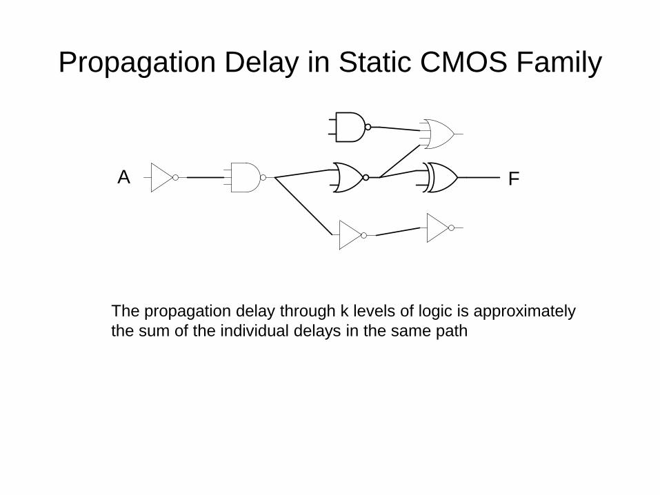
A F
The propagation delay through k levels of logic is approximately
the sum of the individual delays in the same path

Propagation Delay in Static CMOS Family
A FStage 1 Stage 2 Stage 3 Stage 4
tHL=tHL4+tLH3+tHL2+tLH1
Example:
tLH=tLH4+tHL3+tLH2+tHL1
tPROP=tLH+tHL=(tLH4+tHL3+tLH2+tHL1)+ (tHL4+tLH3+tHL2+tLH1)
tPROP=tLH+tHL=(tLH4+tHL4)+(tLH3+tHL3)+ (tLH2+tHL2)+(tLH1+tHL1)
tPROP=tPROP4+tPROP3+tPROP2+tPROP1

Propagation Delay in Static CMOS Family
F
A
Propagation through k levels of logic
HL HLk LH(k-1) XY1HL k-2t t + t + t + ••• + t
LH LHk HL(k-1) YX1LH k-2t t + t + t + ••• + t
where x=H and Y=L if k odd and X=L and Y=h if k even
1 PROP PROPkt t
k
i
Will return to propagation delay after we discuss device sizing

Digital Circuit Design
• Hierarchical Design
• Basic Logic Gates
• Properties of Logic Families
• Characterization of CMOS
Inverter
• Static CMOS Logic Gates
– Ratio Logic
• Propagation Delay
– Simple analytical models
– Elmore Delay
• Sizing of Gates
• Propagation Delay with
Multiple Levels of Logic
• Optimal driving of Large
Capacitive Loads
• Power Dissipation in Logic
Circuits
• Other Logic Styles
• Array Logic
• Ring Oscillators
done
partial

Device Sizing
Degrees of Freedom?
Strategies?
VOUT
VDD
A1 A2 Ak
A1
A2
Ak
M11 M12 M1k
M21
M22
M2k
VOUT
M1k
M21
VDD
A1 A2 AkM22 M2k
A1
A2
Ak
M2k
M1k
Will consider the inverter first
M1
M2
VDD
VIN VOUT
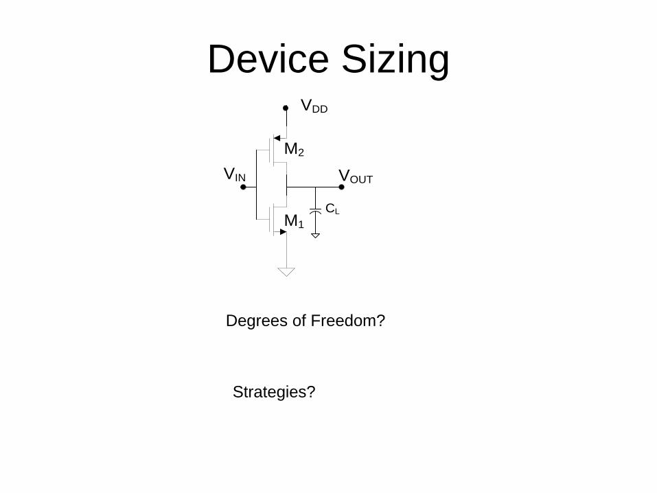
Device Sizing
Degrees of Freedom?
Strategies?
M1
M2
VDD
VIN VOUT
CL
Device Sizing
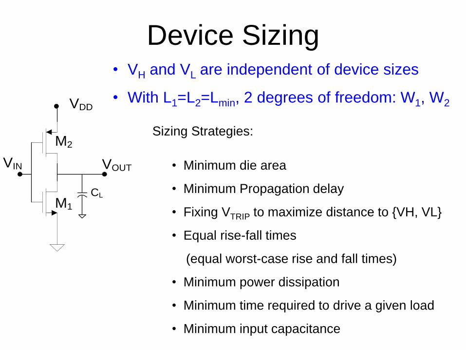
• Minimum die area
• Minimum Propagation delay
• Fixing VTRIP to maximize distance to {VH, VL}
• Equal rise-fall times
(equal worst-case rise and fall times)
• Minimum power dissipation
• Minimum time required to drive a given load
• Minimum input capacitance
Sizing Strategies:
• VH and VL are independent of device sizes
• With L1=L2=Lmin, 2 degrees of freedom: W1, W2
M1
M2
VDD
VIN VOUT
CL

Device Sizing
Sizing Strategy: minimum sized
2211OXIN LWLWCC
TnDD1OXn
1PD
VVWCμ
LR
TpDD2OXp
2PU
VVWCμ
LR
M1
M2
VDD
VIN VOUT
CL
Assume VTn=0.2VDD, VTp=-0.2VDD, μn/μp=3, L1=L2=Lmin
Wn=?, Wp=?, Vtrip=?,tHL=?,tLH=?
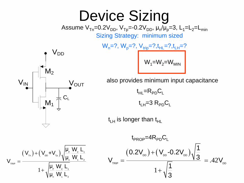
Device Sizing
W1=W2=WMIN
also provides minimum input capacitance
42
1
DD DD DD
TRIP DD
10.2V V -0.2V
3V . V1
3
tHL=RPDCL
tLH=3 RPDCL
Sizing Strategy: minimum sized
M1
M2
VDD
VIN VOUT
CL
Wn=?, Wp=?, Vtrip=?,tHL=?,tLH=?
Assume VTn=0.2VDD, VTp=-0.2VDD, μn/μp=3, L1=L2=Lmin
tPROP=4RPDCL
tLH is longer than tHL
1
p 2 1
Tn DD Tp
n 1 2
TRIP
p 2 1
n 1 2
μ W LV V +V
μ W LV
μ W L
μ W L

Device Sizing
Sizing strategy: Equal (worst case) rise and fall times
M1
M2
VDD
VIN VOUT
CL
Assume VTn=0.2VDD, VTp=-0.2VDD, μn/μp=3, L1=L2=Lmin
min
PDn OX 1 DD
LR
μ C W 0.8V
min
PUn OX 2 DD
LR
3μ C W 0.8V
Wn=?, Wp=?, Vtrip=?,tHL=?,tLH=?

Device Sizing
2
1
3m
m n
p
W
W
PU INLHPU PD
HL PD IN
R Ct= R =R
t R C
Thus
VTRIP=?
What about the second degree of freedom?
1 2
n OX 1 DD Tn p OX 2 DD Tp
L L
u C W V -V u C W V +V
with L1=L2 and VTp=-VTn we must have
Sizing strategy: Equal (worst case) rise and fall times
M1
M2
VDD
VIN VOUT
CL
Assume VTn=0.2VDD, VTp=-0.2VDD, μn/μp=3, L1=L2=Lmin
W1=WMIN
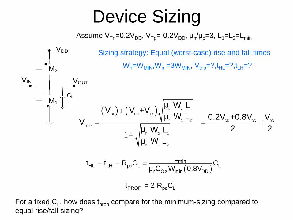
Device Sizing
1
p 2 1
Tn DD Tp
n 1 2 DD DD DD
TRIP
p 2 1
n 1 2
μ W LV V +V
μ W L 0.2V +0.8V VV =
2 2μ W L
μ W L
Sizing strategy: Equal (worst-case) rise and fall times
M1
M2
VDD
VIN VOUT
CL
Assume VTn=0.2VDD, VTp=-0.2VDD, μn/μp=3, L1=L2=Lmin
Wn=WMIN,Wp =3WMIN, Vtrip=?,tHL=?,tLH=?
min
HL LH pd L Ln OX min DD
Lt = t = R C C
μ C W 0.8V
PROP pd Lt = 2 R C
For a fixed CL, how does tprop compare for the minimum-sizing compared to
equal rise/fall sizing?

Device Sizing
Sizing strategy: Fixed VTRIP= VDD/2
M1
M2
VDD
VIN VOUT
CL
Assume VTn=0.2VDD, VTp=-0.2VDD, μn/μp=3, L1=L2=Lmin
Wn=?, Wp=?, Vtrip=?,tHL=?,tLH=?

Device Sizing
1
p 2 1
DD DD DD
n 1 2 DD
TRIP
p 2 1
n 1 2
μ W L.2V V - .2V
μ W L VV =
2μ W L
μ W L
Set VTRIP=VDD/2
Solving, obtain
Sizing strategy: Fixed VTRIP=VDD/2
• This is the same sizing as was obtained for equal worst-case
rise and fall times so tHL=tLH=RpdCL
• This is no coincidence !!! Why?
• These properties guide the definition of the process parameters provided
by the foundry
2
1
n
p
W
W
m
m
M1
M2
VDD
VIN VOUT
CL
Assume VTn=0.2VDD, VTp=-0.2VDD, μn/μp=3, L1=L2=Lmin
Wn=?, Wp=? , Vtrip=?,tHL=?,tLH=?
Wn=WMIN, Wp =3WMIN

Device Sizing
• Minimum die area
• Minimum Propagation delay
• Fixing VTRIP to maximize distance to {VH, VL}
• Equal rise-fall times
(equal worst-case rise and fall times)
• Minimum power dissipation
• Minimum time required to drive a given load
• Minimum input capacitance
Sizing Strategies:
• VH and VL are independent of device sizes
• With L1=L2=Lmin, 2 degrees of freedom: W1, W2
M1
M2
VDD
VIN VOUT
CL

Device Sizing
Sizing Strategy Summary
Minimum Size VTRIP=VDD/2 Equal
Rise/Fall
Size Wn=Wp=Wmin
Lp=Ln=Lmin
Wn=Wmin
Wp=3Wmin
Lp=Ln=Lmin
Wn=Wmin
Wp=3Wmin
Lp=Ln=Lmin
tHL RpdCL RpdCL RpdCL
tLH 3RpdCL RpdCL RpdCL
tPROP 4RpdCL 2RpdCL 2RpdCL
Vtrip VTRIP=0.42VDD VTRIP=0.5VDD VTRIP=0.5VDD
M1
M2
VDD
VIN VOUT
CL
Assume VTn=0.2VDD, VTp=-0.2VDD, μn/μp=3, L1=L2=Lmin
• For a fixed load CL, the minimum-sized structure has a higher tPROP
• If the load is another inverter, CL is half, so tPROP remain the same
• This will be investigated later

Reference InverterAssume μn/μp=3
Ln=Lp=LMIN
Wn=WMIN, Wp=3WnThe reference inverter
VIN VOUT
M1
M2
VDD
CL
• Have sized the reference inverter with Wp/Wn=μn/μp
• In standard processes, provides VTRIP ≈ VDD/2 and tHL ≈ tLH
• Any other sizing strategy could have been used for the
reference inverter but this is most convenient
REF INREF OX MIN MINdef
C = C = 4C W L
Tn DDV =.2VMIN MIN
PDREF
n OX MIN DD Tn n OX MIN DD
L LR
μ C W V -V μ C W 0.8V
Tp DDV = -.2V
MINPUREF PDREF
p OX MIN DD Tp
LR R
μ C 3W V +V

Reference InverterAssume μn/μp=3
Ln=Lp=LMIN
Wn=WMIN, Wp=3WnThe reference inverter pair
L1 REF OX MIN MINC = C =4C W L
VIN
VOUT
M1
M2
VDD
M1
M2
VDD
CL
V’OUT
CL1
REF PROPREF HLREF LHREF PDREF REFdef
t = t = t +t =2R C

Reference Inverter
REF OX MIN MINC = 4C W L
Assume μn/μp=3
Ln=Lp=LMIN
Wn=WMIN, Wp=3Wn
REF PDREF REFt =2R C
The reference inverter pair
REF OX MIN MINC =4C W L
VIN
VOUT
M1
M2
VDD
M1
M2
VDD
CL
V’OUT
CL1
Summary: parameters defined from reference inverter:
VIN VOUT
M1
M2
VDD
CL
MIN
PDREF
n OX MIN DD Tn
LR =
μ C W V -V

The Reference Inverter
REF IN OX MIN MINC =C = 4C W L
REF HLREF LHREF PDREF REFt = t + t = 2R C
VIN
VOUT
M1
M2
VDD
Wn=WMIN, Wp=3WMIN
Assume μn/μp=3
Reference Inverter
Ln=Lp=LMIN
In 0.5u proc tREF=20ps,
CREF=4fF, RPDREF=RPUREF=2.5K
HLREF LHREF PDREF REFt = t = R C
(Note: This COX is somewhat larger than that in the 0.5u ON process)
PDREF PUREFR =R
.2MIN MIN
PDREF
n OX MIN DD Tn n OX MIN DD
L LR =
μ C W V -V μ C W 0.8V
Tn DDV V

Propagation Delay
How does the propagation delay compare for a minimum-sized strategy
to that of an equal rise/fall sizing strategy?
VIN
VOUT
M1
M2
VDD
M1
M2
VDD
CL
V’OUT
CL1
VIN
VOUT
M1
M2
VDD
M1
M2
VDD
CL
V’OUT
CL1
Minimum Sized Reference Inverter
W2=W1=WMIN W2=(µn/µp)W1, W1=WMIN
PROP REFt = t

Device Sizing
REF OX MIN MINC = 4C W L
.2
0.8PDREFR
Tn DDV VMIN MIN
n OX MIN DD Tn n OX MIN DD
L L
C W V V C W Vm m
Assume μn/μp=3
Ln=Lp=LMIN
Wn=WMIN, Wp=Wn
2PROP HLREF LHREF PDREF REF PDREF REF PDREF REFt =t +t =R 0.5C 3R 0.5C R C
The minimum-sized inverter pair
L1 REF OX MIN MINC = 0.5C =2C W LVIN
VOUT
M1
M2
VDD
M1
M2
VDD
CL
V’OUT
CL1
P R O P R E F Ft = t

By how much did tHL improve?
Why was there no net change in tPROP?
Propagation DelayHow does the propagation delay compare for a minimum-sized strategy
to that of an equal rise/fall sizing strategy?
VIN
VOUT
M1
M2
VDD
M1
M2
VDD
CL
V’OUT
CL1
VIN
VOUT
M1
M2
VDD
M1
M2
VDD
CL
V’OUT
CL1
Minimum Sized Reference Inverter
W2=W1=WMINW2=(µn/µp)W1, W1=WMIN
PROP REFt = tPROP REFt = t
Even though the tLH rise time has been reduced with the equal rise/fall sizing
strategy, this was done at the expense of an increase in the total load capacitance
that resulted in no net change in propagation delay!
They are the same!

Device Sizing
VINVOUT
M1
M2
VDD
VOUT
VDD
A1 A2 Ak
A1
A2
Ak
M11 M12 M1k
M21
M22
M2k
VOUT
M1k
M21
VDD
A1 A2 AkM22 M2k
A1
A2
Ak
M2k
M1k
Will consider now the multiple-input gates
Will consider both minimum sizing and equal worst-case rise/fall
Will assume CL (not shown)=CREF
Note: worst-case has been added since fall time in NOR gates or rise
time in NAND gates depends upon how many transistors are conducting
Will initially size so gate drive capability is same as that of ref inverter

Fan In• The Fan In (FI) to an input of a gate device, circuit or interconnect
that is capacitive is the input capacitance
• Often this is normalized to some capacitance (typically CREF of ref inverter).
ININ
REF
CFI =C alternately FI
C

Sizing of Multiple-Input Gates
Analysis strategy : Express delays in terms of those of reference inverter
REF HLREF LHREF PDREF REFt = t + t = 2R C
VIN
VOUT
M1
M2
VDD
Wn=WMIN, Wp=3WMIN
Assume μn/μp=3
Reference Inverter
Ln=Lp=LMIN
In 0.5u proc tREF=20ps,
CREF=4fF,RPDREF=2.5K
HLREF LHREF PDREF REFt = t =R C

Device SizingMultiple Input Gates:
2-input NOR
Fastest response (tHL or tLH) = ?
Wn=?
Wp=?
Equal Worst Case Rise/Fall (and equal to that of ref inverter when driving CREF)
Input capacitance (FI) = ?
Minimum Sized (assume driving a load of CREF)
Wn=Wmin
Wp=Wmin
Fastest response (tHL or tLH) = ?
Slowest response (tHL or tLH) = ?
Input capacitance (FI) = ?
Worst case response (tPROP, usually of most interest)?
Worst case response (tPROP, usually of most interest)?
2-input NAND k-input NOR k-input NAND
A
B
C
VDD
CREF
VOUT
VDD
A1 A2 Ak
A1
A2
Ak
M11 M12 M1k
M21
M22
M2k
CREF
VDD
B
A C
CREF
VOUT
M1k
M21
VDD
A1 A2 AkM22 M2k
A1
A2
Ak
M2k
M1k
CREF

Device Sizing
Multiple Input Gates: 2-input NOR
DERIVATIONSWn=?
Wp=?
Equal Worst Case Rise/Fall (and equal to that of ref inverter when driving CREF)
Input capacitance = ?
FI=?
tPROP=? (worst case)
(n-channel devices sized same, p-channel devices sized the same)
Assume Ln=Lp=Lmin and driving a load of CREF
A
B
C
VDD
CREF
Wn=WMIN
Wp=6WMIN
INA INB OX MIN MIN OX MIN MIN OX MIN MIN OX MIN MIN REF7 7
C =C =C W L +6C W L =7C W L = 4C W L = C4 4
REF7 7
FI= C FI=4 4
or
tPROP = tREF (worst case)
One degree of freedom was used to
satisfy the constraint indicated
Other degree of freedom was used to
achieve equal rise and fall times
Device Sizing
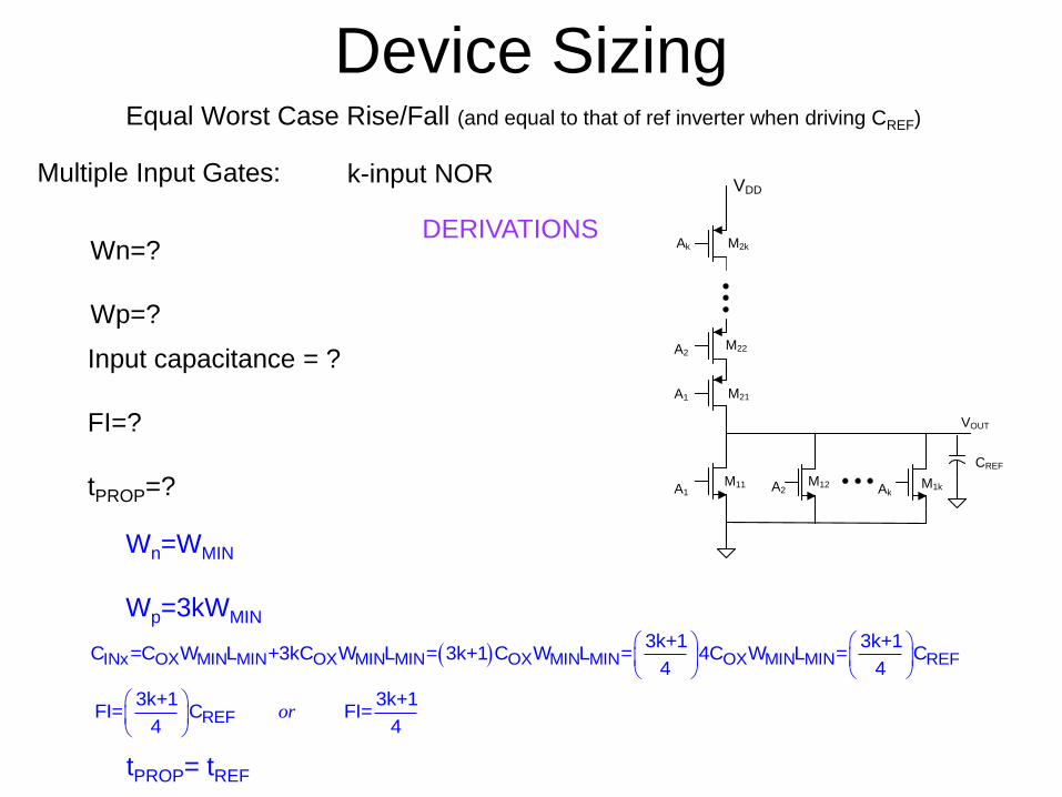
Multiple Input Gates: k-input NOR
DERIVATIONS
Equal Worst Case Rise/Fall (and equal to that of ref inverter when driving CREF)
Wn=?
Wp=?
Input capacitance = ?
FI=?
tPROP=?
Wn=WMIN
Wp=3kWMIN
INx OX MIN MIN OX MIN MIN OX MIN MIN OX MIN MIN REF3k+1 3k+1
C =C W L +3kC W L = 3k+1 C W L = 4C W L = C4 4
REF3k+1 3k+1
FI= C FI=4 4
or
tPROP= tREF
VOUT
VDD
A1 A2 Ak
A1
A2
Ak
M11 M12 M1k
M21
M22
M2k
CREF
Device Sizing
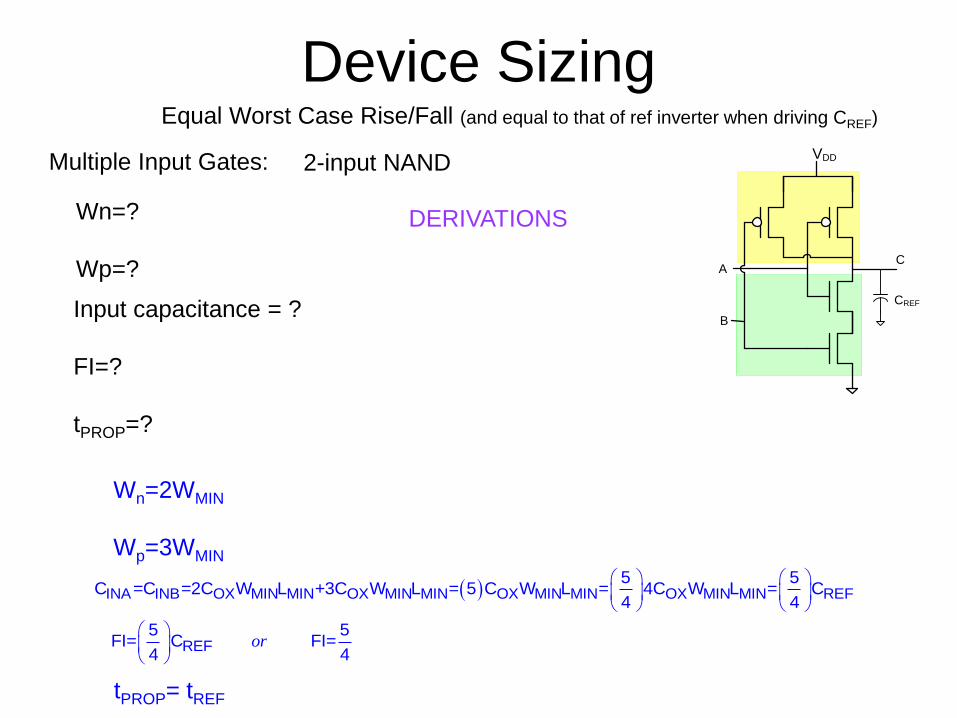
Multiple Input Gates: 2-input NAND
DERIVATIONS
Equal Worst Case Rise/Fall (and equal to that of ref inverter when driving CREF)
Wn=?
Wp=?
Input capacitance = ?
FI=?
tPROP=?
VDD
B
A C
CREF
Wn=2WMIN
Wp=3WMIN
INA INB OX MIN MIN OX MIN MIN OX MIN MIN OX MIN MIN REF5 5
C =C =2C W L +3C W L = 5 C W L = 4C W L = C4 4
REF5 5
FI= C FI=4 4
or
tPROP= tREF

Device Sizing
Multiple Input Gates: k-input NAND
DERIVATIONS
Equal Worst Case Rise/Fall (and equal to that of ref inverter when driving CREF)
Wn=?
Wp=?
Input capacitance = ?
FI=?
tPROP=?
Wn=kWMIN
Wp=3WMIN
INx OX MIN MIN OX MIN MIN OX MIN MIN OX MIN MIN REF3+k 3+k
C =kC W L +3C W L = 3+k C W L = 4C W L = C4 4
REF3+k 3+k
FI= C FI=4 4
or
tPROP= tREF
VOUT
M1k
M21
VDD
A1 A2 AkM22 M2k
A1
A2
Ak
M2k
M1k
CREF
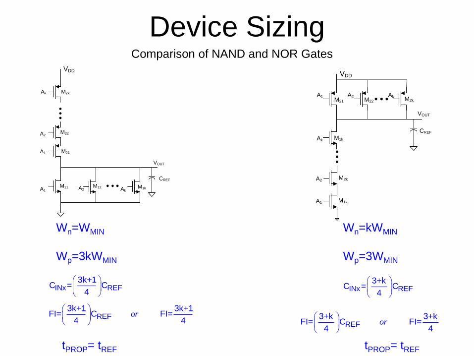
Device SizingComparison of NAND and NOR Gates
INx REF3+k
C = C4
REF3+k 3+k
FI= C FI=4 4
or
Wn=kWMIN
Wp=3WMIN
Wn=WMIN
Wp=3kWMIN
INx REF3k+1
C = C4
REF3k+1 3k+1
FI= C FI=4 4
or
tPROP= tREF tPROP= tREF
VOUT
VDD
A1 A2 Ak
A1
A2
Ak
M11 M12 M1k
M21
M22
M2k
CREF
VOUT
M1k
M21
VDD
A1 A2 AkM22 M2k
A1
A2
Ak
M2k
M1k
CREF
Device Sizing
IN REFC =C
Assume μn/μp=3
Ln=Lp=LMIN
Wn=WMIN, Wp=3WMIN
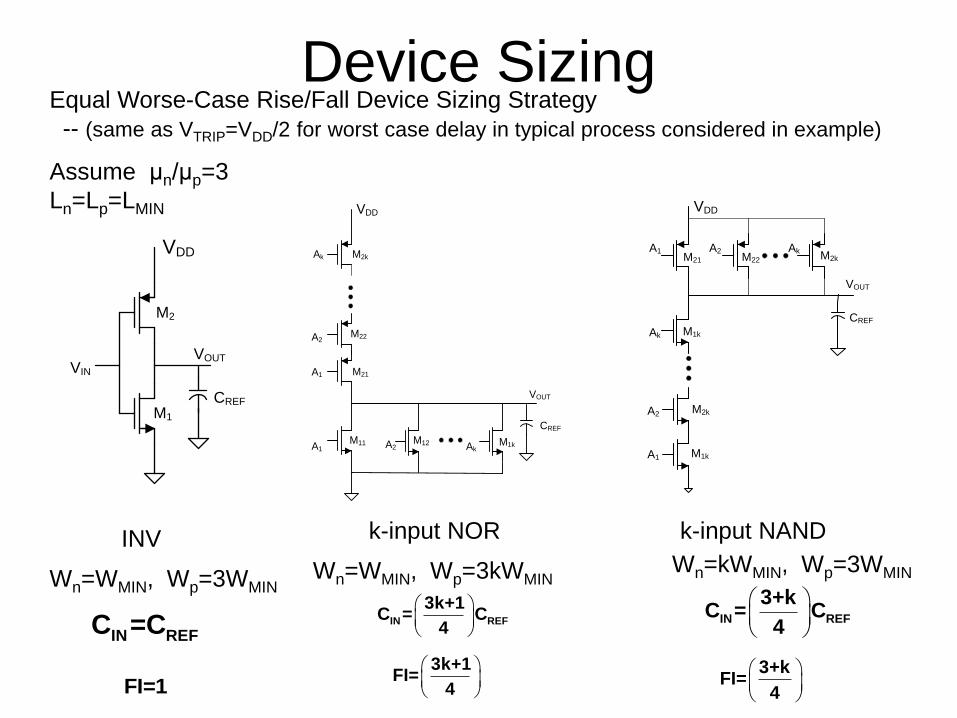
Equal Worse-Case Rise/Fall Device Sizing Strategy
-- (same as VTRIP=VDD/2 for worst case delay in typical process considered in example)
k-input NANDINV k-input NOR
Wn=WMIN, Wp=3kWMINWn=kWMIN, Wp=3WMIN
IN REF
3k+1C = C
4
IN REF
3+kC = C
4
VIN
VOUT
M1
M2
VDD
CREF
VOUT
M1k
M21
VDD
A1 A2 AkM22 M2k
A1
A2
Ak
M2k
M1k
CREF
VOUT
VDD
A1 A2 Ak
A1
A2
Ak
M11 M12 M1k
M21
M22
M2k
CREF
FI=1
3k+1FI=
4
3+kFI=
4

Device SizingMultiple Input Gates:
2-input NOR
Fastest response (tHL or tLH) = ?
Wn=?
Wp=?
Equal Worst Case Rise/Fall (and equal to that of ref inverter when driving CREF)
Input capacitance (FI) = ?
Minimum Sized (assume driving a load of CREF)
Wn=Wmin
Wp=Wmin
Fastest response (tHL or tLH) = ?
Slowest response (tHL or tLH) = ?
Input capacitance (FI) = ?
Worst case response (tPROP, usually of most interest)?
Worst case response (tPROP, usually of most interest)?
2-input NAND k-input NOR k-input NAND
A
B
C
VDD
CREF
VOUT
VDD
A1 A2 Ak
A1
A2
Ak
M11 M12 M1k
M21
M22
M2k
CREF
VDD
B
A C
CREF
VOUT
M1k
M21
VDD
A1 A2 AkM22 M2k
A1
A2
Ak
M2k
M1k
CREF

Device Sizing
Minimum Sized (assume driving a load of CREF) Wn=Wmin Wp=Wmin
Fastest response (tHL or tLH) = ?
Slowest response (tHL or tLH) = ?
Input capacitance (FI) = ?
Worst case response (tPROP, usually of most interest)?
VOUT
VDD
A1 A2 Ak
A1
A2
Ak
M11 M12 M1k
M21
M22
M2k
CREF
VOUT
M1k
M21
VDD
A1 A2 AkM22 M2k
A1
A2
Ak
M2k
M1k
CREF
A
B
C
VDD
CREF
VDD
B
A C
CREF
VIN
VOUT
M1
M2
VDD
CREF
REFIN OX n n OX p p OX min min OX min min ox min min
CC = C W L +C W L = C W L + C W L = 2C W L =
21
FI =2

Device Sizing – minimum size driving CREF
k-input NANDINV
k-input NOR
PROPt ?PROPt ?
PROP
3t 0.5
2REF REF
kt t
PROP
3 1t
2REF
kt
PROP
3t
2 2REF REF
kt t
PROP
3t
2REF
kt
REFC
FI = 2
REFC
FI = 2
3PU PDREFR kRPD PDREFR RRPU
= 3RPDREF
RPD
=RPDREF 3PU PDREFR R
VOUT
M1k
M21
VDD
A1 A2 AkM22 M2k
A1
A2
Ak
M2k
M1k
CREF
VIN
VOUT
M1
M2
VDD
CREF VOUT
VDD
A1 A2 Ak
A1
A2
Ak
M11 M12 M1k
M21
M22
M2k
CREF
REFC
FI = 2
PROPt ?
PROPt 2 REFt
PROP
3t 0.5
2REF REFt t
RPD
= kRPDREF

End of Lecture 39


![EE 330 Lecture 42 - Iowa State Universityclass.ece.iastate.edu/ee330/lectures/EE 330 Lect 42 Fall 2016.pdf · EE 330 Lecture 42 Digital Circuits • Elmore Delay ... Elmore delay[1]](https://static.documents.pub/doc/80x56/5b57fe847f8b9a4e1b8b664d/ee-330-lecture-42-iowa-state-330-lect-42-fall-2016pdf-ee-330-lecture-42-digital.jpg)


